TMS 440 SH-3 7708 Microprocessor Support 071-0153-01
100
Instruction Manual TMS 440 SH-3 7708 Microprocessor Support 071-0153-01 Warning The servicing instructions are for use by qualified personnel only. To avoid personal injury, do not perform any servicing unless you are qualified to do so. Refer to all safety summaries prior to performing service.
Transcript of TMS 440 SH-3 7708 Microprocessor Support 071-0153-01

Instruction Manual
TMS 440SH-3 7708 Microprocessor Support
071-0153-01
WarningThe servicing instructions are for use byqualified personnel only. To avoid personalinjury, do not perform any servicing unless youare qualified to do so. Refer to all safetysummaries prior to performing service.

Copyright � Tektronix, Inc. All rights reserved. Licensed software products are owned by Tektronix or its suppliers and areprotected by United States copyright laws and international treaty provisions.
Use, duplication, or disclosure by the Government is subject to restrictions as set forth in subparagraph (c)(1)(ii) of theRights in Technical Data and Computer Software clause at DFARS 252.227-7013, or subparagraphs (c)(1) and (2) of theCommercial Computer Software – Restricted Rights clause at FAR 52.227-19, as applicable.
Tektronix products are covered by U.S. and foreign patents, issued and pending. Information in this publication supercedesthat in all previously published material. Specifications and price change privileges reserved.
Printed in the U.S.A.
Tektronix, Inc., P.O. Box 1000, Wilsonville, OR 97070–1000
TEKTRONIX and TEK are registered trademarks of Tektronix, Inc.

SOFTWARE WARRANTY
Tektronix warrants that the media on which this software product is furnished and the encoding of the programs onthe media will be free from defects in materials and workmanship for a period of three (3) months from the date ofshipment. If a medium or encoding proves defective during the warranty period, Tektronix will provide areplacement in exchange for the defective medium. Except as to the media on which this software product isfurnished, this software product is provided “as is” without warranty of any kind, either express or implied.Tektronix does not warrant that the functions contained in this software product will meet Customer’srequirements or that the operation of the programs will be uninterrupted or error-free.
In order to obtain service under this warranty, Customer must notify Tektronix of the defect before the expirationof the warranty period. If Tektronix is unable to provide a replacement that is free from defects in materials andworkmanship within a reasonable time thereafter, Customer may terminate the license for this software productand return this software product and any associated materials for credit or refund.
THIS WARRANTY IS GIVEN BY TEKTRONIX IN LIEU OF ANY OTHER WARRANTIES, EXPRESSOR IMPLIED. TEKTRONIX AND ITS VENDORS DISCLAIM ANY IMPLIED WARRANTIES OFMERCHANTABILITY OR FITNESS FOR A PARTICULAR PURPOSE. TEKTRONIX’RESPONSIBILITY TO REPLACE DEFECTIVE MEDIA OR REFUND CUSTOMER’S PAYMENT ISTHE SOLE AND EXCLUSIVE REMEDY PROVIDED TO THE CUSTOMER FOR BREACH OF THISWARRANTY. TEKTRONIX AND ITS VENDORS WILL NOT BE LIABLE FOR ANY INDIRECT,SPECIAL, INCIDENTAL, OR CONSEQUENTIAL DAMAGES IRRESPECTIVE OF WHETHERTEKTRONIX OR THE VENDOR HAS ADVANCE NOTICE OF THE POSSIBILITY OF SUCHDAMAGES.

HARDWARE WARRANTY
Tektronix warrants that the products that it manufactures and sells will be free from defects in materials andworkmanship for a period of one (1) year from the date of shipment. If a product proves defective during thiswarranty period, Tektronix, at its option, either will repair the defective product without charge for parts and labor,or will provide a replacement in exchange for the defective product.
In order to obtain service under this warranty, Customer must notify Tektronix of the defect before the expirationof the warranty period and make suitable arrangements for the performance of service. Customer shall beresponsible for packaging and shipping the defective product to the service center designated by Tektronix, withshipping charges prepaid. Tektronix shall pay for the return of the product to Customer if the shipment is to alocation within the country in which the Tektronix service center is located. Customer shall be responsible forpaying all shipping charges, duties, taxes, and any other charges for products returned to any other locations.
This warranty shall not apply to any defect, failure or damage caused by improper use or improper or inadequatemaintenance and care. Tektronix shall not be obligated to furnish service under this warranty a) to repair damageresulting from attempts by personnel other than Tektronix representatives to install, repair or service the product;b) to repair damage resulting from improper use or connection to incompatible equipment; c) to repair anydamage or malfunction caused by the use of non-Tektronix supplies; or d) to service a product that has beenmodified or integrated with other products when the effect of such modification or integration increases the timeor difficulty of servicing the product.
THIS WARRANTY IS GIVEN BY TEKTRONIX IN LIEU OF ANY OTHER WARRANTIES, EXPRESSOR IMPLIED. TEKTRONIX AND ITS VENDORS DISCLAIM ANY IMPLIED WARRANTIES OFMERCHANTABILITY OR FITNESS FOR A PARTICULAR PURPOSE. TEKTRONIX’RESPONSIBILITY TO REPAIR OR REPLACE DEFECTIVE PRODUCTS IS THE SOLE ANDEXCLUSIVE REMEDY PROVIDED TO THE CUSTOMER FOR BREACH OF THIS WARRANTY.TEKTRONIX AND ITS VENDORS WILL NOT BE LIABLE FOR ANY INDIRECT, SPECIAL,INCIDENTAL, OR CONSEQUENTIAL DAMAGES IRRESPECTIVE OF WHETHER TEKTRONIX ORTHE VENDOR HAS ADVANCE NOTICE OF THE POSSIBILITY OF SUCH DAMAGES.

TMS 440 SH-3 7708 Microprocessor Support i
Table of Contents
General Safety Summary v. . . . . . . . . . . . . . . . . . . . . . . . . . . . . . . . . . . .
Service Safety Summary vii. . . . . . . . . . . . . . . . . . . . . . . . . . . . . . . . . . . . . Preface ix. . . . . . . . . . . . . . . . . . . . . . . . . . . . . . . . . . . . . . . . . . . . . . . . . . . Manual Conventions ix. . . . . . . . . . . . . . . . . . . . . . . . . . . . . . . . . . . . . . . . . . . . . . Logic Analyzer Documentation x. . . . . . . . . . . . . . . . . . . . . . . . . . . . . . . . . . . . . . Contacting Tektronix x. . . . . . . . . . . . . . . . . . . . . . . . . . . . . . . . . . . . . . . . . . . . . .
Getting StartedSupport Package Description 1–1. . . . . . . . . . . . . . . . . . . . . . . . . . . . . . . . . . . . . . . . Logic Analyzer Software Compatibility 1–2. . . . . . . . . . . . . . . . . . . . . . . . . . . . . . . Logic Analyzer Configuration 1–2. . . . . . . . . . . . . . . . . . . . . . . . . . . . . . . . . . . . . . . Requirements and Restrictions 1–2. . . . . . . . . . . . . . . . . . . . . . . . . . . . . . . . . . . . . . . Configuring the Probe Adapter 1–4. . . . . . . . . . . . . . . . . . . . . . . . . . . . . . . . . . . . . . Connecting to a System Under Test With A Probe Adapter 1–4. . . . . . . . . . . . . . . . Connect the P6434 Probes to the Probe Adapter 1–5. . . . . . . . . . . . . . . . . . . . . . . . . Connect the Test Clip to the Probe Adapter 1–6. . . . . . . . . . . . . . . . . . . . . . . . . . . . . Connect the Probe Adapter Assembly to the System Under Test 1–6. . . . . . . . . . . . Removing the Probe Adapter from the SUT 1–8. . . . . . . . . . . . . . . . . . . . . . . . . . . . Connecting to a System Under Test Without A Probe Adapter 1–8. . . . . . . . . . . . . . Applying and Removing Power 1–9. . . . . . . . . . . . . . . . . . . . . . . . . . . . . . . . . . . . . Functionality Not Supported 1–10. . . . . . . . . . . . . . . . . . . . . . . . . . . . . . . . . . . . . . . . Channel Assignments 1–10. . . . . . . . . . . . . . . . . . . . . . . . . . . . . . . . . . . . . . . . . . . . . CPU To Mictor Connections 1–16. . . . . . . . . . . . . . . . . . . . . . . . . . . . . . . . . . . . . . . .
Operating BasicsSetting Up the Support 2–1. . . . . . . . . . . . . . . . . . . . . . . . . . . . . . . . . . . . . . Channel Group Definitions 2–1. . . . . . . . . . . . . . . . . . . . . . . . . . . . . . . . . . . . . . . . . Clocking Options 2–1. . . . . . . . . . . . . . . . . . . . . . . . . . . . . . . . . . . . . . . . . . . . . . . . .
Custom Clocking 2–1. . . . . . . . . . . . . . . . . . . . . . . . . . . . . . . . . . . . . . . . . . . . . Symbols 2–9. . . . . . . . . . . . . . . . . . . . . . . . . . . . . . . . . . . . . . . . . . . . . . . . . . . . . . . .
Acquiring and Viewing Disassembled Data 2–11. . . . . . . . . . . . . . . . . . . . . Acquiring Data 2–11. . . . . . . . . . . . . . . . . . . . . . . . . . . . . . . . . . . . . . . . . . . . . . . . . . . Viewing Disassembled Data 2–11. . . . . . . . . . . . . . . . . . . . . . . . . . . . . . . . . . . . . . . .
Hardware Display Format 2–12. . . . . . . . . . . . . . . . . . . . . . . . . . . . . . . . . . . . . . . Software Display Format 2–13. . . . . . . . . . . . . . . . . . . . . . . . . . . . . . . . . . . . . . . Control Flow Display Format 2–13. . . . . . . . . . . . . . . . . . . . . . . . . . . . . . . . . . . . Subroutine Display Format 2–14. . . . . . . . . . . . . . . . . . . . . . . . . . . . . . . . . . . . . .
Changing How Data is Displayed 2–14. . . . . . . . . . . . . . . . . . . . . . . . . . . . . . . . . . . . Optional Display Selections 2–14. . . . . . . . . . . . . . . . . . . . . . . . . . . . . . . . . . . . . Marking Cycles 2–16. . . . . . . . . . . . . . . . . . . . . . . . . . . . . . . . . . . . . . . . . . . . . . . Displaying Exception Vectors 2–17. . . . . . . . . . . . . . . . . . . . . . . . . . . . . . . . . . . .
Viewing an Example of Disassembled Data 2–17. . . . . . . . . . . . . . . . . . . . . . . . . . . .

Table of Contents
ii TMS 440 SH-3 7708 Microprocessor Support
SpecificationsMaintenance
Probe Adapter Circuit Description 4–1. . . . . . . . . . . . . . . . . . . . . . . . . . . . . . . . . . . . Replacing Signal Leads 4–1. . . . . . . . . . . . . . . . . . . . . . . . . . . . . . . . . . . . . . . . . . . . Replacing Protective Sockets 4–2. . . . . . . . . . . . . . . . . . . . . . . . . . . . . . . . . . . . . . . . Replacing the Fuse 4–2. . . . . . . . . . . . . . . . . . . . . . . . . . . . . . . . . . . . . . . . . . . . . . . .
Replaceable Electrical PartsParts Ordering Information 5–1. . . . . . . . . . . . . . . . . . . . . . . . . . . . . . . . . . . . . . . . . Using the Replaceable Electrical Parts List 5–1. . . . . . . . . . . . . . . . . . . . . . . . . . . . .
Diagrams
Replaceable Mechanical PartsParts Ordering Information 7–1. . . . . . . . . . . . . . . . . . . . . . . . . . . . . . . . . . . . . . . . . Using the Replaceable Mechanical Parts List 7–1. . . . . . . . . . . . . . . . . . . . . . . . . . .
Index

Table of Contents
TMS 440 SH-3 7708 Microprocessor Support iii
List of Figures
Figure 1–1: Jumper locations on the probe adapter 1–4. . . . . . . . . . . . . .
Figure 1–2: Connecting probes to a probe adapter 1–5. . . . . . . . . . . . . . . Figure 1–3: Seating the test clip on the probe adapter 1–6. . . . . . . . . . . .
Figure 1–4: Placing the probe adapter assembly onto the SUT 1–7. . . . . Figure 1–5: Location of the power jack 1–9. . . . . . . . . . . . . . . . . . . . . . . . .
Figure 1–6: Pin assignments for a Mictor connector (component side) 1–16. . .
Figure 2–1: SRAM/ROM/PCMCIA Access bus timing 2–3. . . . . . . . . . . .
Figure 2–2: DRAM Access bus timing 2–4. . . . . . . . . . . . . . . . . . . . . . . . . .
Figure 2–3: EDO DRAM Access bus timing 2–5. . . . . . . . . . . . . . . . . . . . . Figure 2–4: SDRAM Read bus timing 2–6. . . . . . . . . . . . . . . . . . . . . . . . . .
Figure 2–5: SDRAM Write bus timing 2–7. . . . . . . . . . . . . . . . . . . . . . . . . Figure 2–6: PSRAM Access bus timing 2–8. . . . . . . . . . . . . . . . . . . . . . . . .
Figure 2–7: SDRAM Mode Register Write Cycles bus timing 2–9. . . . . . Figure 2–8: Hardware display format 2–15. . . . . . . . . . . . . . . . . . . . . . . . . .
Figure 3–1: Dimensions of the probe adapter 3–4. . . . . . . . . . . . . . . . . . . .
Figure 4–1: Location of the fuse 4–2. . . . . . . . . . . . . . . . . . . . . . . . . . . . . . .
Figure 5–1: SH–3 7708 probe adapter exploded view 7–5. . . . . . . . . . . . .

Table of Contents
iv TMS 440 SH-3 7708 Microprocessor Support
List of Tables
Table 1–1: Address channel group assignments 1–10. . . . . . . . . . . . . . . . .
Table 1–2: Data channel group assignments 1–12. . . . . . . . . . . . . . . . . . . . Table 1–3: Control channel group assignments 1–13. . . . . . . . . . . . . . . . . .
Table 1–4: Chip_Sel channel group assignments 1–13. . . . . . . . . . . . . . . . . Table 1–5: Control2 channel group assignments 1–14. . . . . . . . . . . . . . . . .
Table 1–6: WEN channel group assignments 1–14. . . . . . . . . . . . . . . . . . . . Table 1–7: Misc channel group assignments 1–14. . . . . . . . . . . . . . . . . . . .
Table 1–8: Signals that are on the probe adapter but not acquired 1–15. . Table 1–9: CPU to Mictor connections for Mictor A pins 1–17. . . . . . . . .
Table 1–10: CPU to Mictor connections for Mictor D pins 1–18. . . . . . . .
Table 1–11: CPU to Mictor connections for Mictor C pins 1–19. . . . . . . .
Table 2–1: Control group symbol table definitions 2–10. . . . . . . . . . . . . . . Table 2–2: Meaning of special characters in the display 2–11. . . . . . . . . .
Table 2–3: Cycle type definitions 2–12. . . . . . . . . . . . . . . . . . . . . . . . . . . . . Table 2–4: Exception vectors for Addressing mode 2–17. . . . . . . . . . . . . .
Table 3–1: Electrical specifications 3–1. . . . . . . . . . . . . . . . . . . . . . . . . . . .
Table 3–2: Environmental specifications 3–3. . . . . . . . . . . . . . . . . . . . . . .

TMS 440 SH-3 7708 Microprocessor Support v
General Safety Summary
Review the following safety precautions to avoid injury and prevent damage tothis product or any products connected to it. To avoid potential hazards, use thisproduct only as specified.
Only qualified personnel should perform service procedures.
While using this product, you may need to access other parts of the system. Readthe General Safety Summary in other system manuals for warnings and cautionsrelated to operating the system.
Use Proper Power Cord. Use only the power cord specified for this product andcertified for the country of use.
Connect and Disconnect Properly. Do not connect or disconnect probes or testleads while they are connected to a voltage source.
Ground the Product. This product is indirectly grounded through the groundingconductor of the mainframe power cord. To avoid electric shock, the groundingconductor must be connected to earth ground. Before making connections to theinput or output terminals of the product, ensure that the product is properlygrounded.
Observe All Terminal Ratings. To avoid fire or shock hazard, observe all ratingsand marking on the product. Consult the product manual for further ratingsinformation before making connections to the product.
The common terminal is at ground potential. Do not connect the commonterminal to elevated voltages.
Do not apply a potential to any terminal, including the common terminal, thatexceeds the maximum rating of that terminal.
Use Proper AC Adapter. Use only the AC adapter specified for this product.
Do Not Operate Without Covers. Do not operate this product with covers or panelsremoved.
Use Proper Fuse. Use only the fuse type and rating specified for this product.
Avoid Exposed Circuitry. Do not touch exposed connections and componentswhen power is present.
Do Not Operate With Suspected Failures. If you suspect there is damage to thisproduct, have it inspected by qualified service personnel.
Do Not Operate in Wet/Damp Conditions.
Do Not Operate in an Explosive Atmosphere.
To Avoid Fire or Personal Injury

General Safety Summary
vi TMS 440 SH-3 7708 Microprocessor Support
Keep Product Surfaces Clean and Dry.
Provide Proper Ventilation. Refer to the manual’s installation instructions fordetails on installing the product so it has proper ventilation.
Terms in this Manual. These terms may appear in this manual:
WARNING. Warning statements identify conditions or practices that could resultin injury or loss of life.
CAUTION. Caution statements identify conditions or practices that could result indamage to this product or other property.
Terms on the Product. These terms may appear on the product:
DANGER indicates an injury hazard immediately accessible as you read themarking.
WARNING indicates an injury hazard not immediately accessible as you read themarking.
CAUTION indicates a hazard to property including the product.
Symbols on the Product. The following symbols may appear on the product:
Protective Ground(Earth) Terminal
CAUTIONRefer to Manual
Double Insulated
WARNINGHigh Voltage
Symbols and Terms

TMS 440 SH-3 7708 Microprocessor Support vii
Service Safety Summary
Only qualified personnel should perform service procedures. Read this ServiceSafety Summary and the General Safety Summary before performing any serviceprocedures.
Do Not Service Alone. Do not perform internal service or adjustments of thisproduct unless another person capable of rendering first aid and resuscitation ispresent.
Disconnect Power. To avoid electric shock, switch off the instrument power, thendisconnect the power cord from the mains power.
Use Care When Servicing With Power On. Dangerous voltages or currents mayexist in this product. Disconnect power, remove battery (if applicable), anddisconnect test leads before removing protective panels, soldering, or replacingcomponents.
To avoid electric shock, do not touch exposed connections.

Service Safety Summary
viii TMS 440 SH-3 7708 Microprocessor Support

TMS 440 SH-3 7708 Microprocessor Support ix
Preface
This instruction manual contains specific information about the TMS 440SH-3 7708 microprocessor support package and is part of a set of information onhow to operate this product on compatible Tektronix logic analyzers.
If you are familiar with operating microprocessor support packages on the logicanalyzer for which the TMS 440 SH-3 7708 support was purchased, you willonly need this instruction manual to set up and run the support.
If you are not familiar with operating microprocessor support packages, you willneed to supplement this instruction manual with information on basic operationsto set up and run the support.
Information on basic operations of microprocessor support packages is includedwith each product. Each logic analyzer includes basic information that describeshow to perform tasks common to support packages on that platform. Thisinformation can be in the form of online help, an installation manual, or a usermanual.
This manual provides detailed information on the following topics:
� Connecting the logic analyzer to the system under test
� Setting up the support to acquire data from the system under test
� Acquiring and viewing disassembled data
Manual ConventionsThis manual uses the following conventions:
� The term “disassembler” refers to the software that disassembles bus cyclesinto instruction mnemonics and cycle types.
� The phrase “information on basic operations” refers to online help, aninstallation manual, or a user manual covering the basic operations ofmicroprocessor supports.
� In the information on basic operations, the term “XXX” or “P54C” appearingin field selections and file names must be replaced with SH-3. This term isthe name of the microprocessor in field selections and file names you mustuse to operate the SH-3 7708 support.
� The term “SUT” (system under test) refers to the microprocessor-basedsystem from which data will be acquired.

Preface
x TMS 440 SH-3 7708 Microprocessor Support
� The term “logic analyzer” refers to the Tektronix logic analyzer for whichthis product was purchased.
� The term “module” refers to an acquisition module.
� The term “HI module” refers to the module in the higher-numbered slot, andthe term “LO module” refers to the module in the lower-numbered slot.
� SH-3 refers to all supported variations of the SH-3 7708 microprocessorunless otherwise noted.
� A tilde (~) following a signal name indicate an active low signal.
Logic Analyzer DocumentationA description of other documentation available for each type of Tektronix logicanalyzer is located in the user manual of the corresponding module. The manualset provides the information necessary to install, operate, maintain, and servicethe logic analyzer and its associated products.
Contacting Tektronix
ProductSupport
For questions about using Tektronix measurement products, calltoll free in North America:1-800-TEK-WIDE (1-800-835-9433 ext. 2400)6:00 a.m. – 5:00 p.m. Pacific time
Or contact us by e-mail:[email protected]
For product support outside of North America, contact yourlocal Tektronix distributor or sales office.
ServiceSupport
Tektronix offers extended warranty and calibration programs asoptions on many products. Contact your local Tektronixdistributor or sales office.
For a listing of worldwide service centers, visit our web site.
For otherinformation
In North America:1-800-TEK-WIDE (1-800-835-9433)An operator will direct your call.
To write us
Website
Tektronix, Inc.P.O. Box 1000Wilsonville, OR 97070-1000USA
Tektronix.com

Getting Started


TMS 440 SH-3 7708 Microprocessor Support 1–1
Getting Started
This chapter contains information on the following topics and tasks:
� A description of the TMS 440 microprocessor support package
� Logic analyzer software compatibility
� Support restrictions
� How to connect to the system under test (SUT)
� Your system under test requirements
� How to apply power to and remove power from the probe adapter
Support Package DescriptionThe TMS 440 microprocessor support package displays disassembled data from asystem based on the Hitachi Micro Systems, Inc SH-3 7708 microprocessor.
The support runs on a TLA 700 Series logic analyzer equipped with a 102-chan-nel module.
Refer to information on basic operations to determine how many modules andprobes your logic analyzer needs to meet the minimum channel requirements forthe TMS 440 microprocessor support.
A complete list of standard and optional accessories is provided at the end of theparts list in the Replaceable Parts chapter.
To use this support efficiently, you need to have the items listed in the informa-tion on basic operations as well as the following documents:
� SH7700 Series Programming Manual, Hitachi Micro Systems, Inc 8/8/95ADE–602–096
� SH7708 Hardware User Manual, Hitachi Micro Systems, Inc 9/10/96ADE–602–105A
� SH–3 Series Memory Interfacing, Hitachi Micro Systems, Inc 11/22/96
Information on basic operations also contains a general description of support.Contact Tektronix for the availability of SH-3 7702 Support.

Getting Started
1–2 TMS 440 SH-3 7708 Microprocessor Support
Logic Analyzer Software Compatibility
The floppy disk label on the microprocessor support states which version of logicanalyzer software this support is compatible with.
Logic Analyzer Configuration To use the SH-3 7708 support, the TLA 700 Series logic analyzer must beequipped with a 102-channel module at a minimum. The module must beequipped with enough probes to acquire channel and clock data from signals inyour SH-3 7708-based system.
Refer to information on basic operations to determine how many modules andprobes the logic analyzer needs to meet the channel requirements.
For the TLA 700 Series logic analyzer, the TMS 440 channel assignments followthe standard channel mapping and labeling scheme for P6434 probes. Follow theprocedure to apply labels, using the standard method as described in the P6434Mass Termination Probe Instructions.
Requirements and RestrictionsYou should review the general requirements and restrictions of microprocessorsupport packages in the information on basic operations as they pertain to yourSUT.
You should also review electrical, environmental, and mechanical specificationsin Specifications in this manual as they pertain to your system under test, as wellas the following descriptions of other SH-3 7708 support requirements andrestrictions.
System Clock Rate. The SH-3 7708 microprocessor support can acquire data fromthe SH-3 7708 microprocessor operating at tested speeds of up to 60 MHz. Thisspecification is valid at the time this manual was printed. Please contact yourTektronix Sales Representative for current information on the fastest devicessupported.

Getting Started
TMS 440 SH-3 7708 Microprocessor Support 1–3
Channel groups. The following table lists the SH-3 signals not required by theClocking State Machine (CSM) or disassembler. SH-3 signals may be removedfrom their default connections and reattached to other signals of interest. Channelgroups not required for clocking and disassembly are:
Signal name Section:channel
CKE C3–5
IOIS16~ C3–1
WAIT~ C0–2
IRQOUT~ C2–5
NMI~ C2–4
IRL0~ C0–3
IRL1~ C0–7
IRL2~ C3–0
IRL3~ C3–4
SUT Power. Whenever the SUT is powered off, remove power from the probeadapter. Refer to Applying and Removing Power on page 1–9 for information onhow to remove power from the probe adapter.
Alternate Bus Master. Alternate bus master transactions are not processed in thedisassembly.
Data Disassembly. For correct data display disassembly turn off (disable) thecache and the MMU address translation.
When the Address translation is enabled flushing could be incorrect (MMU pagebreaks interpreted as address breaks).
Byte Invalidation. Invalid bytes cannot be dashed out for reads from SRAM/PSRAM/ROM/PCMCIA interfaces.
Opcode Fetch/Data Read. SH-3 7708 does not provide a signal to distinguishbetween “Data Read” and “Opcode Fetch”. The TMS 440 does make a reason-able estimate at looking a few sequences ahead at the address values yet in someinstances you may need to use the “Mark Opcode” function.

Getting Started
1–4 TMS 440 SH-3 7708 Microprocessor Support
Configuring the Probe Adapter There are six jumpers on the probe adapter. The default position for all sixjumpers is between pin 1 and pin 2 (See Figure 1–1). The custom clocking andacquisition software-setup choices function correctly when the jumpers are in thedefault position. Pin 2 of each jumper is connected to the logic analyzer throughthe Mictor connectors. These six jumpers are intended for future use.
Default position for jumpers
J241
J145
J144J143
J142
J141
Figure 1–1: Jumper locations on the probe adapter
Connecting to a System Under Test With A Probe Adapter Before you connect to the SUT (System Under Test), connect the probes to themodule. Your SUT must also have a minimum amount of clear space surround-ing the microprocessor to accommodate the probe adapter.
To connect the logic analyzer to a SUT using a probe adapter, follow these steps:
1. Turn off the power to your SUT. It is not necessary to turn off the logicanalyzer.
CAUTION. Static discharge can damage the microprocessor, the probe adapter,the probes, and the module. To prevent static damage, handle these componentsonly in a static-free environment.
Always wear a grounding wrist strap, heel strap, or similar device whilehandling the microprocessor and probe adapter.

Getting Started
TMS 440 SH-3 7708 Microprocessor Support 1–5
2. To discharge your stored static electricity, touch the ground connector locatedon the back of the logic analyzer. Then, touch any of the ground pins of theprobe adapter to discharge stored static electricity from the probe adapter.
3. Connect the P6434 probes to the probe adapter as shown in Figure 1–2.Match the channel groups and numbers on the probe labels to the corre-sponding pins on the probe adapter. Match the ground pins on the probes tothe corresponding pins on the probe adapter.
Pin 1
Figure 1–2: Connecting probes to a probe adapter
Connect the P6434 Probes to the Probe
Adapter

Getting Started
1–6 TMS 440 SH-3 7708 Microprocessor Support
4. Carefully seat the test clip on the PGA socket pins on the underside of theprobe adapter as shown in Figure 1–3. Refer to the Converter Clip Instruc-tions included with the probe adapter for more information about the testclip.
Hold the probe adapterin one hand, align theQFP test clip with thepins, and press on byapplying even pressureon all sides of the clip;be sure the clip iscompletely seated.
QFP144 test clip
Figure 1–3: Seating the test clip on the probe adapter
5. Inspect the microprocessor on your SUT for bent or broken leads. Verify thatthe leads on the microprocessor are clean and free from dirt, dust, or anyforeign material.
6. Inspect the pins of the test clip for bent or broken contacts. Verify that theleads on the test clip are clean and free from dirt, dust or any foreignmaterial.
7. Verify that the locking devise on the test clip is not locked by pushing andturning the locking device counterclockwise.
CAUTION. Failure to correctly place the probe adapter assembly onto themicroprocessor can permanently damage all electrical components when poweris applied.
Center the clip on the microprocessor and apply an equal downward force on allfour sides of the clip, slightly rocking the probe adapter in a clockwise circle.
Do not apply leverage to the probe adapter when installing or removing it.
Connect the Test Clip tothe Probe Adapter
Connect the ProbeAdapter Assembly to the
System Under Test

Getting Started
TMS 440 SH-3 7708 Microprocessor Support 1–7
8. Place the probe adapter onto the SUT as shown in Figure 1–4.
Pin 1
SUT
Pin 1
Test clip
ProbeAdapter
Figure 1–4: Placing the probe adapter assembly onto the SUT
9. Lock the test clip to the microprocessor by pushing and turning the lockingdevice clockwise.
CAUTION. The test clip was designed to be used on one and only one micropro-cessor. Because of the tight tolerances required for QFP test clip connectivity, thetest clip that attaches to the microprocessor has a soft plastic collar thatconforms to the unique shape of the target microprocessor.
To avoid faulty and unreliable connections, it is highly recommended that the testclip is not used on any other microprocessor then the one it was originallyconnected to.
The test clip has a manufacturer’s stated life expectancy of 8–10 connections.

Getting Started
1–8 TMS 440 SH-3 7708 Microprocessor Support
CAUTION. The probe adapter board might slip off or slip to one side of themicroprocessor because of the extra weight of the probes. This can damage themicroprocessor and the SUT. To prevent this from occurring, stabilize the probeadapter by placing a nonconductive object (such as foam) between the probeadapter and the SUT.
10. Unlock the test clip from the microprocessor by pushing and turning thelocking device counterclockwise.
11. Gently lift and pull the probe adapter off of the microprocessor.
Connecting to a System Under Test Without A Probe AdapterYou can use channel probes, clock probes, and leadsets with a commercial testclip (or adapter) to make connections between the logic analyzer and your SUT.
To connect the probes to SH-3 7708 signals in the SUT using a test clip, followthese steps:
1. Turn off power to your SUT. It is not necessary to turn off power to the logicanalyzer.
CAUTION. Static discharge can damage the microprocessor, the probes, and thelogic analyzer module. To prevent static damage, handle these components onlyin a static-free environment.
Always wear a grounding wrist strap, heel strap, or similar device whilehandling the microprocessor.
2. To discharge your stored static electricity, touch the ground connector locatedon the back of the logic analyzer. If you are using a test clip, touch any of theground pins on the clip to discharge stored static electricity from it.
CAUTION. Failure to place the SUT on a horizontal surface before connecting thetest clip can permanently damage the pins on the microprocessor.
3. Place the SUT on a horizontal static-free surface.
4. Use Table 1–1 through Table 1–8 to connect the channel probes toSH-3 7708 signal pins on the test clip or in the SUT.
Use leadsets to connect at least one ground lead from each channel probe andthe ground lead from each clock probe to ground pins on your test clip.
Removing the ProbeAdapter from the SUT

Getting Started
TMS 440 SH-3 7708 Microprocessor Support 1–9
Applying and Removing Power A power supply for the SH-3 7708 probe adapter is included with this micropro-cessor support. The power supply provides +5 volts power to the probe adapter.
To apply power to the SH-3 7708 probe adapter and SUT, follow these steps:
CAUTION. Failure to use the +5 V power supply provided by Tektronix canpermanently damage the probe adapter and SH-3 7708 microprocessor. Do notuse any otherpower supply for the +5 V power supply.
1. Connect the +5 V power supply to the jack on the probe adapter. Figure 1–5shows the location of the jack on the adapter board.
CAUTION. Failure to apply power to the probe adapter before applying power toyour SUT can permanently damage the SH-3 7708 microprocessor and SUT.
2. Plug the power supply for the probe adapter into an electrical outlet. Whenpower is present on the probe adapter, an LED lights near the power jack.
3. Power on the SUT.
PowerJack
Figure 1–5: Location of the power jack
To remove power from the SUT and SH-3 7708 probe adapter, follow thesesteps:

Getting Started
1–10 TMS 440 SH-3 7708 Microprocessor Support
CAUTION. Failure to power down your SUT before removing the power from theprobe adapter might permanently damage the SH-3 7708 microprocessor andSUT.
1. Power off the SUT.
2. Unplug the power supply for the probe adapter from the electrical outlet.
Functionality Not Supported
Microprocessor. The cache must be turned off (disabled) for proper disassembly.
MMU address translation. The MMU address translation must be turned off forproper disassembly. When Address translation is enabled Flushing could beincorrect(MMU page breaks are interpreted as address breaks).
Channel Assignments Channel assignments shown in Table 1–1 through Table 1–8 use the followingconventions:
� All signals are required by the support unless indicated otherwise.
� Channels are shown starting with the most significant bit (MSB), descendingto the least significant bit (LSB).
� Channel group assignments are for all modules unless otherwise noted.
� A tilde (~) following a signal name indicates an active low signal.
� An equals sign (=) following a signal name indicates that it is double probed.
� The module in the higher-numbered slot is referred to as the HI module andthe module in the lower-numbered slot is referred to as the LO module.
Table 1–1 shows the probe section and channel assignments for the Addressgroup and the microprocessor signal to which each channel connects. By defaultthe Address channel group assignments are displayed in hexadecimal.
Table 1–1: Address channel group assignments
Bit order Section:channel SH-3 7708 signal name
31 A3:7 CS6~/CE1B~
30 A3:6 CS5~/CE1A~

Getting Started
TMS 440 SH-3 7708 Microprocessor Support 1–11
Table 1–1: Address channel group assignments (cont.)
Bit order SH-3 7708 signal nameSection:channel
29 A3:5 CS4~
28 A3:4 CS3~
27 A3:3 CS2~
26 A3:2 CS1~
25 A3:1 A25
24 A3:0 A24
23 A2:7 A23
22 A2:6 A22
21 A2:5 A21
20 A2:4 A20
19 A2:3 A19
18 A2:2 A18
17 A2:1 A17
16 A2:0 A16
15 A1:7 A15
14 A1:6 A14
13 A1:5 A13
12 A1:4 A12
11 A1:3 A11
10 A1:2 A10
9 A1:1 A9
8 A1:0 A8
7 A0:7 A7
6 A0:6 A6
5 A0:5 A5
4 A0:4 A4
3 A0:3 A3
2 A0:2 A2
1 A0:1 A1
0 A0:0 A0

Getting Started
1–12 TMS 440 SH-3 7708 Microprocessor Support
Table 1–2 shows the probe section and channel assignments for the Data groupand the microprocessor signal to which each channel connects. By default theData channel group assignments are displayed in hexadecimal.
Table 1–2: Data channel group assignments
Bit order Section:channel SH-3 7708 signal name
31 D3:7 D31
30 D3:6 D30
29 D3:5 D29
28 D3:4 D28
27 D3:3 D27
26 D3:2 D26
25 D3:1 D25
24 D3:0 D24
23 D2:7 D23/Port7
22 D2:6 D22/Port6
21 D2:5 D21/Port5
20 D2:4 D20/Port4
19 D2:3 D19/Port3
18 D2:2 D18/Port2
17 D2:1 D17/Port1
16 D2:0 D16/Port0
15 D1:7 D15
14 D1:6 D14
13 D1:5 D13
12 D1:4 D12
11 D1:3 D11
10 D1:2 D10
9 D1:1 D9
8 D1:0 D8
7 D0:7 D7
6 D0:6 D6
5 D0:5 D5
4 D0:4 D4
3 D0:3 D3
2 D0:2 D2
1 D0:1 D1
0 D0:0 D0

Getting Started
TMS 440 SH-3 7708 Microprocessor Support 1–13
Table 1–3 shows the probe section and channel assignments for the Controlgroup and the microprocessor signal to which each channel connects. By defaultthe Control channel group assignments are displayed as symbols. The symboltable file name is SH–3_Ctrl.
Table 1–3: Control channel group assignments
Bit order Section:channel SH-3 7708 signal name
10 Clk:3 L_BS~
9 Clk:1 L_RAS~
8 C2–3 DL_RASD~
7 Clk:2 L_CAS~
6 C2–0 DL_CASD~
5 C2–2 DL_WER~
4 C3–3 RD/WR~
3 C1–4 CASHH~/CAS2H~
2 C1–0 CASHL~/CAS2L~
1 C0–4 CASLH~
0 C0–0 CASLL~/CAS~/OE~
Table 1–4 shows the probe section and channel assignments for the CHip_Selgroup and the microprocessor signal to which each channel connects. By default,this channel group is not displayed.
Table 1–4: Chip_Sel channel group assignments
Bit order Section:channel SH-3 7708 signal name
8 C3–6 MD4/CE2B~
7 C3–2 MD3/CE2A~
6 A3–7 CS6~/CE1B~
5 A3–6 CS5~/CE1A~
4 A3–5 CS4~
3 A3–4 CS3~
2 A3–3 CS2~
1 A3–2 CS1~
0 C2–6 CS0~

Getting Started
1–14 TMS 440 SH-3 7708 Microprocessor Support
Table 1–5 shows the probe section and channel assignments for the Control2group and the microprocessor signal to which each channel connects. By default,this channel group is not displayed.
Table 1–5: Control2 channel group assignments
Bit order Section:channel SH-3 7708 signal name
5 C1–3 RAS~/CE~
4 C1–7 MD5/RAS2~
3 C1–4 CASHH~/CAS2H~
2 C1–0 CASHL~/CAS2L~
1 C0–4 CASLH~
0 C0–0 CASLL~/CAS~/OE~
Table 1–6 shows the probe section and channel assignments for the WEN groupand the microprocessor signal to which each channel connects. By default, thischannel group is not displayed.
Table 1–6: WEN channel group assignments
Bit order Section:channel SH-3 7708 signal name
3 C1–5 WE3~/DQMUU~/ICIOWR~
2 C1–1 WE2~/DQMUL~/ICIORD~
1 C0–5 WE1~/DQMLU~
0 C0–1 WE0~/DQMLL~
Table 1–7 shows the probe section and channel assignments for the Misc groupand the microprocessor signal to which each channel connects. By default, thischannel group is not displayed.
Table 1–7: Misc channel group assignments
Bit order Section:channel SH-3 7708 signal name
15 C1–6 STATUS1
14 C1–2 STATUS0
13 C0–6 BACK~
12 C2–1 DL_STAT
11 C0–2 WAIT~
10 C3–1 IOIS16~
9 C3–5 CKE

Getting Started
TMS 440 SH-3 7708 Microprocessor Support 1–15
Table 1–7: Misc channel group assignments (cont.)
Bit order SH-3 7708 signal nameSection:channel
8 C2–5 IRQOUT~
7 Clk–0 CKIO
6 C2–7 BS~
5 C2–4 NMI
4 C0–3 IRL0~
3 C0–7 IRL1~
2 C3–0 IRL2~
1 C3–4 IRL3~
0 C3–7 RD~
Table 1–8 shows the signals on the probe adapter but not acquired.
Table 1–8: Signals that are on the probe adapter but not acquired
Signal Name Pin Number
MD2/RXD 84
MD1/TXD 85
MD0/SCK 86
BREQ~ 87
RESET~ 88
TCLK 134
EXTAL 79
XTAL 80
CAP1 74
CAP2 77
XTAL2 136
EXTAL2 137
Nonintrusive Acquisition. The SH-3 7708 will not intercept, modify, or returnsignals to the system under test.
Acquisition Setup. The TMS 440 will affect the logic analyzer setup menus (andsubmenus) by modifying existing fields and adding micro-specific fields.

Getting Started
1–16 TMS 440 SH-3 7708 Microprocessor Support
The TMS 440 will add the selection “SH-3” to the Load Support Package dialogbox, located under the File pull-down menu. Once that “SH-3 support” has beenloaded, the “Custom” clocking mode selection in the module Setup menu is alsoenabled.
CPU To Mictor Connections To probe the microprocessor you will need to make connections between theCPU and the Mictor pins of the P6434 Mass Termination Probe. Refer to theP6434 Mass Termination Probe manual, Tektronix part number 070-9793-xx, formore information on mechanical specifications. Tables 1–9 through 1–11 showthe CPU pin to Mictor pin connections.
Tektronix uses a counter-clockwise pin assignment. Pin-1 is located at the topleft, and pin-2 is located directly below it. Pin-20 is located on the bottom right,and pin-21 is located directly above it.
AMP uses an odd side-even side pin assignment. Pin-1 is located at the top left,and pin-3 is located directly below it. Pin-2 is located on the top right, and pin-4is located directly below it.
NOTE. When designing Mictor connectors into your SUT, always follow theTektronix pin assignment.
Pin 1
Pin 19
Pin 38
Pin 20
Pin 2
Pin 38
Pin 1
Pin 37
Tektronix Pinout AMP Pinout
Figure 1–6: Pin assignments for a Mictor connector (component side)
Please pay close attention to the caution below.
CAUTION. To protect the CPU and the inputs of the module, it is recommendedthat a 180� resistor is connected in series between each ball pad of the CPU andeach pin of the Mictor connector. The resistor must be no farther away from theball pad of the CPU than 1/2-inch.

Getting Started
TMS 440 SH-3 7708 Microprocessor Support 1–17
Table 1–9: CPU to Mictor connections for Mictor A pins
TektronixMictor A pin number
AMPMictor A pin number LA channel SH-3 signal name
SH-3 7708pin number
1 1 NC NC NC
2 3 NC NC NC
3 5 CLK:0 CKIO 101
4 7 A3:7 CS6~/CE1B~ 108
5 9 A3:6 CS5~/CE1A~ 109
6 11 A3:5 CS4~ 110
7 13 A3:4 CS3~ 111
8 15 A3:3 CS2~ 112
9 17 A3:2 CS1~ 113
10 19 A3:1 A25 72
11 21 A3:0 A24 71
12 23 A2:7 A23 70
13 25 A2:6 A22 67
14 27 A2:5 A21 66
15 29 A2:4 A20 65
16 31 A2:3 A19 64
17 33 A2:2 A18 63
18 35 A2:1 A17 62
19 37 A2:0 A16 61
20 38 A0:0 A0 37
21 36 A0:1 A1 38
22 34 A0:2 A2 39
23 32 A0:3 A3 40
24 30 A0:4 A4 43
25 28 A0:5 A5 44
26 26 A0:6 A6 45
27 24 A0:7 A7 46
28 22 A1:0 A8 47
29 20 A1:1 A9 48
30 18 A1:2 A10 51
31 16 A1:3 A11 52
32 14 A1:4 A12 53
33 12 A1:5 A13 56
34 10 A1:6 A14 57

Getting Started
1–18 TMS 440 SH-3 7708 Microprocessor Support
Table 1–9: CPU to Mictor connections for Mictor A pins (cont.)
TektronixMictor A pin number
SH-3 7708pin numberSH-3 signal nameLA channel
AMPMictor A pin number
35 8 A1:7 A15 58
36 6 CLK:1 L_RAS~ –
37 4 NC NC NC
38 2 NC NC NC
39 39 GND GND GND
40 40 GND GND GND
41 41 GND GND GND
42 42 GND GND GND
43 43 GND GND GND
Table 1–10: CPU to Mictor connections for Mictor D pins
TektronixMictor D pin number
AMPMictor D pin number LA channel SH-3 signal name
SH-3 7708pin number
1 1 NC NC NC
2 3 NC NC NC
3 5 NC NC NC
4 7 D3:7 D31 140
5 9 D3:6 D30 141
6 11 D3:5 D29 142
7 13 D3:4 D28 143
8 15 D3:3 D27 1
9 17 D3:2 D26 2
10 19 D3:1 D25 3
11 21 D3:0 D24 4
12 23 D2:7 D23/Port7 5
13 25 D2:6 D22/Port6 8
14 27 D2:5 D21/Port5 9
15 29 D2:4 D20/Port4 10
16 31 D2:3 D19/Port3 11
17 33 D2:2 D18/Port2 12
18 35 D2:1 D17/Port1 13
19 37 D2:0 D16/Port0 14

Getting Started
TMS 440 SH-3 7708 Microprocessor Support 1–19
Table 1–10: CPU to Mictor connections for Mictor D pins (cont.)
TektronixMictor D pin number
SH-3 7708pin numberSH-3 signal nameLA channel
AMPMictor D pin number
20 38 D0:0 D0 36
21 36 D0:1 D1 35
22 34 D0:2 D2 34
23 32 D0:3 D3 33
24 30 D0:4 D4 32
25 28 D0:5 D5 29
26 26 D0:6 D6 28
27 24 D0:7 D7 27
28 22 D1:0 D8 26
29 20 D1:1 D9 25
30 18 D1:2 D10 24
31 16 D1:3 D11 23
32 14 D1:4 D12 22
33 12 D1:5 D13 21
34 10 D1:6 D14 16
35 8 D1:7 D15 15
36 6 CLK:2 L_CAS~ –
37 4 NC NC NC
38 2 NC NC NC
39 39 GND GND GND
40 40 GND GND GND
41 41 GND GND GND
42 42 GND GND GND
43 43 GND GND GND
Table 1–11: CPU to Mictor connections for Mictor C pins
TektronixMictor C pin number
AMPMictor C pin number LA channel SH-3 signal name
SH-3 7708pin number
1 1 NC NC NC
2 3 NC NC NC
3 5 CLK–3 L_BS~ –

Getting Started
1–20 TMS 440 SH-3 7708 Microprocessor Support
Table 1–11: CPU to Mictor connections for Mictor C pins (cont.)
TektronixMictor C pin number
SH-3 7708pin numberSH-3 signal nameLA channel
AMPMictor C pin number
4 7 C3:7 RD~ 107
5 9 C3:6 MD4/CE2B~ 103
6 11 C3:5 CKE 131
7 13 C3:4 IRL3~ 90
8 15 C3:3 RD/WR~ 106
9 17 C3:2 MD3/CE2A~ 104
10 19 C3:1 IOIS16~ 94
11 21 C3:0 IRL2~ 91
12 23 C2:7 BS~ 105
13 25 C2:6 CSO~ 114
14 27 C2:5 IRQOUT~ 95
15 29 C2:4 NMI 89
16 31 C2:3 DL_RASD~ –
17 33 C2:2 DL_WER~ –
18 35 C2:1 DL_STAT –
19 37 C2:0 DL_CASD~ –
20 38 C0:0 CASLL~/CAS~/OE~ 126
21 36 C0:1 WE0~/DQMLL~ 124
22 34 C0:2 WAIT~ 132
23 32 C0:3 IRL0~ 93
24 30 C0:4 CASLH~ 125
25 28 C0:5 WE1~/DQMLU~ 123
26 26 C0:6 BACK~ 96
27 24 C0:7 IRL1~ 92
28 22 C1:0 CASHL~/CAS2L~ 120
29 20 C1:1 WE2~/DQMUL~/ICIORD~ 118
30 18 C1:2 STATUS0 98
31 16 C1:3 RAS~/CE~ 129
32 14 C1:4 CASHH~/CAS2H~ 119
33 12 C1:5 WE3~/DQMUU~/ICIOWR~ 117
34 10 C1:6 STATUS1 97

Getting Started
TMS 440 SH-3 7708 Microprocessor Support 1–21
Table 1–11: CPU to Mictor connections for Mictor C pins (cont.)
TektronixMictor C pin number
SH-3 7708pin numberSH-3 signal nameLA channel
AMPMictor C pin number
35 8 C1:7 MD5/RAS2~ 130
36 6 NC NC NC
37 4 NC NC NC
38 2 NC NC NC
39 39 GND GND GND
40 40 GND GND GND
41 41 GND GND GND
42 42 GND GND GND
43 43 GND GND GND

Getting Started
1–22 TMS 440 SH-3 7708 Microprocessor Support

Operating Basics


TMS 440 SH-3 7708 Microprocessor Support 2–1
Setting Up the Support
The information in this section is specific to the operations and functions of theTMS 440 SH-3 7708 support on any Tektronix logic analyzer for which it can bepurchased.
Before you acquire and display disassembled data, you need to load the supportand specify the setups for clocking and triggering as described in the informationon basic operations. The microprocessor support provides default values for eachof these setups as well as user-definable settings.
Channel Group Definitions The software automatically defines channel groups for the support. The channelgroups for the SH-3 7708 support are Address, Data, Control, Chip_Sel,Control2, WEN, and Misc. If you want to know which signal is in which group,refer to the channel assignment tables beginning on page 1–10.
Clocking OptionsThe TMS 440 support offers a microprocessor-specific clocking mode for theSH-3 7708 microprocessor. This clocking mode is the default selection wheneveryou load the SH-3 support.
Disassembly will not be correct with the Internal or External clocking modes.Information on basic operations describes how to use these clock selections forgeneral-purpose analysis.
A special clocking program is loaded to the module every time you load theSH-3 support. This special clocking is called Custom.
In Custom clocking, the CSM (Clocking State Machine) generates one mastersample for each microprocessor bus cycle, no matter how many clock cycles arecontained in the bus cycle.
The Custom clocking for the SH-3 7708 processor has a Clock_option to takeyour input from the memory type connected to physical space areas 2 and 3.
The memory types for which the SH-3 7708 can provide Control signals areSRAM, Burst ROM, PCMCIA, DRAM, EDO DRAM, Puesdo-SRAM, andSDRAM.
The Control signals for these memories share pins. For example,WE3~/DQMUU/ICIOWR~ is used for SRAM, Puesdo-SRAM, and SDRAM and
Custom Clocking

Setting Up the Support
2–2 TMS 440 SH-3 7708 Microprocessor Support
is also used for the PCMCIA memories. Also, some qualifiers are latched on therising edge of CKIO and some on the falling edge of CKIO. The qualifierslatched on the rising edge of CKIO are:
L_BS~, L_RAS~, L_CAS~ and DL_STAT
The qualifiers latched on the falling edge of CKIO are:
DL_RASD~, DL_CASD~ and DL_WER~
The TMS 440 has four modes of acquisition clocking. There is one select fieldwith the following label:
Memory Type:
that will contain the following selections:
DRAM/PSRAM/NORMAL1 Cycles from those memories are acquired.(default)
SDRAM/NORMAL1 Cycles from those memories are acquired.
EDODRAM/NORMAL1 Cycles from those memories are acquired.
A2–DRAM/A3–EDODRAM/NORMAL1 Cycles from Physical area2 – DRAM
and area3 – EDODRAM are acquired.
1 NORMAL means SRAM/ROM/PCMCIA interfaces

Setting Up the Support
TMS 440 SH-3 7708 Microprocessor Support 2–3
SRAM/ROM/PCMCIA Access. SRAM/ROM/PCMCIA accesses are handled by allfour clocking options. The Address, Data, and Control signals are logged-inevery trailing CKIO edge when the DL_WER~ qualifier is low, until theDL_WER~ goes high. When the DL_WER~ is high at the next rising CKIO edgeit is mastered. The DL_WER~ for these cycles will go from low to high after atrailing edge of CKIO and before the rising edge of CKIO see figure 2–1.
CKIO
L_BS~
Address A25–A0
RD~ (Asserted for Read )
Address
DataData
WEn~ (Asserted for Write)
DL_WER~(Asserted forboth Read and Write)
A ; D ; C
M ;
Figure 2–1: SRAM/ROM/PCMCIA Access bus timing

Setting Up the Support
2–4 TMS 440 SH-3 7708 Microprocessor Support
DRAM Access. DRAM accesses are handled by DRAM/PSRAM/NORMAL orA2–DRAM/A3–EDODRAM/NORMAL clocking options. The Address, Data,and Control signals are logged-in every trailing CKIO edge when theDL_CASD~ and DL_RASD~ qualifiers are low. When the DL_CASD~ is highat the next rising CKIO edge it is mastered. The DL_CASD~ for these cycleswill go from low to high after a trailing edge of CKIO before the rising edge ofCKIO see Figure 2–2.
CKIO
L_BS~
Data
A ; D ; CM ;
Address A25–A16
Address A15–A0
RD/WR~
Row address
Data
Row address Column address
DL_RASD~
DL_CASD~
Figure 2–2: DRAM Access bus timing

Setting Up the Support
TMS 440 SH-3 7708 Microprocessor Support 2–5
EDO DRAM. EDO DRAM accesses are handled by EDODRAM/NORMAL orA2–DRAM/A3–EDODRAM/NORMAL clocking options. The Address, Dataand Control signals are logged-in every rising CKIO edge after the DL_CASD~qualifier is low. In the next trailing edge of CKIO, if DL_CASD~ is high, it ismastered, if DL_CASD~ is low Address, Data, and Control signals are logged-inthe next rising edge of CKIO. The DL_CASD~ for these cycles will go fromlow to high after a trailing edge of CKIO before the rising edge of CKIO seeFigure 2–3.
CKIO
DL_CASD~
Data
A ; M ;
Address A25 - A16
DL_RASD~
Address A15 - A0
RD/WR~
Row address
Data
Row address Column address
L_RAS~
L_BS~
D ; C;
Figure 2–3: EDO DRAM Access bus timing
SDRAM Read. SDRAM accesses are handled by the SDRAM/NORMAL clockingoptions. The Row Address and Control signals are logged-in and mastered at therising CKIO edge if the L_RAS~ is low and if DL_CASD~ and L_CAS~ is highsee Figure 2–4.
In the coming rising edges of CKIO:
a. If the L_CAS~ is low, the Column Address and Control signals arelogged-in and mastered.

Setting Up the Support
2–6 TMS 440 SH-3 7708 Microprocessor Support
b. If L_CAS~ and L_BS~ are low, the Column Address, Data and Controlsignals are logged-in and mastered.
If the Column address is mastered and data has not been acquired, as in the caseof example b, then in the coming rising edges of CKIO if L_BS~ is low,the Data and Control signals are logged-in and mastered. It is possible to haveL_RAS~, L_CAS~, and L_BS~ deasserted between Row Address and ColumnAddress and between Column Address and Data. One of the main differences inthe SDRAM Read cycles and SDRAM Write cycles shown below, is theRD/WR~ behavior.
CKIO
L_CAS~
Data
A ; C ; M ;Row address
D; M ;Data
L_RAS~
Row Address
Data
RD/WR~
L_BS~
Row Address Column Address
A ; C ;M ;Col
address
Row Address ReadCommand
Address A25 - A16
Address A12 - A10
Address A15 - A0
Figure 2–4: SDRAM Read bus timing

Setting Up the Support
TMS 440 SH-3 7708 Microprocessor Support 2–7
CKIO
L_CAS~
Data
A ; C ; M ;Row address
Address A25-A16
L_RAS~
Address A12 or A10
Row Address
Data
RD/WR~
L_BS~
Address A15-A0Row Address ColumnAddress
A ; D; C ; M ;Column address
and Data
Row Address WriteCommand
Figure 2–5: SDRAM Write bus timing
PSRAM Access. PSRAM accesses are handled by DRAM/PSRAM/NORMALclocking option. In PSRAM Read, the Address, Data and Control signals arelogged-in every trailing CKIO edge when the DL_CASD~ AND DL_RASD~qualifiers are low. When the DL_CASD~ is high at the next rising CKIO edge, itis mastered. The DL_CASD~ for these cycles will go from low to high after atrailing edge of CKIO before the rising edge of CKIO.
In PSRAM Write, the Address, Data and Control signals are logged-in everytrailing CKIO edge when the DL_WER~ AND DL_RASD~ qualifiers are low.When the DL_WER~ is high at the next rising CKIO edge, it is mastered.DL_WER~ for these cycles will go from low to high after a trailing edge ofCKIO before the rising edge of CKIO see Figure 2–6.

Setting Up the Support
2–8 TMS 440 SH-3 7708 Microprocessor Support
CKIO
L_BS~
Data
M ;
Address A25-A0
DL_RASD~
Row Address
Data
DL_WER~(Asserted for Write)
A ; D ; C ;
RD/WR~
DL_CASD~(Asserted for Read)
Figure 2–6: PSRAM Access bus timing
SDRAM Mode Register Accesses. SDRAM Mode Register Accesses are handledby the SDRAM/NORMAL clocking options. This access is marked mainly byL_RAS~ and L_CAS~ signals both going low together which does not happenfor normal or burst in Read or Write Cycle types. When L_RAS~ AND L_CAS~are both low at a rising CKIO edge, the Address, Data, and Control signals arelogged-in and mastered see Figure 2–7.

Setting Up the Support
TMS 440 SH-3 7708 Microprocessor Support 2–9
CKIO
CSn~
A ; C ; M; SDMR ROW Addr
RD/WR~
L_RAS~
A12 or A10
A13 or A11
L_CAS~
D31–D0
A ; D ; C ;SDMR ROW Write
M:
Address A25-A16A11 or A2or A9 to A2
Figure 2–7: SDRAM Mode Register Write Cycles bus timing

Setting Up the Support
2–10 TMS 440 SH-3 7708 Microprocessor Support
SymbolsThe TMS 440 support supplies one symbol table file. The SH-3_Ctrl file replacesspecific Control channel group values with symbolic values when Symbolic isthe radix for the channel group.
Symbol tables are generally not for use in timing or SH-3_T support disassembly.
Table 2–1 shows the name, bit pattern, and meaning for the symbols in the fileSH-3_Ctrl, which contains the Control-channel group symbol table.
Table 2–1: Control group symbol table definitions
Control group value
Symbol
L_CAS~ CASHH~L_BS~ DL_CASD~ CASHL~
L_RAS~ DL_WER~ CASLH~DL_RASD~ RD/WR~1 CASLL~ Meaning
”NORMAL READ” � � � � � � � � � � � Memory read from SRAM/ROM/PCMCIA
”NORMAL WRITE” � � � � � � � � � � � Memory write to SRAM/ROM/PCMCIA
”SDRAM COL ADDR” � � � � � � � � � � � SDRAM Column Address
”SDRAM DATA READ” � � � � � � � � � � � SDRAM Data Read
”SDRAM COL ADDR & DATAREAD”
� � � � � � � � � � � SDRAM Column Address access andSDRAM Data Read done simultaneously
”SDRAM DATA WRITE” � � � � � � � � � � � SDRAM Data Write
”SDRAM COL ADDR & DATAWRITE”
� � � � � � � � � � � SDRAM Column Address access andSDRAM Data Write done simultaneously
”SDMR ROW ADDR” � � � � � � � � � � � SDRAM Mode Register Row Address
”SDRAM ROW ADDR” � � � � � � � � � � � SDRAM Row Address
”PSRAM WRITE” � � � � � � � � � � � PSRAM Data Write
”EDO_DRAM / SDMR WRITE” � � � � � � � � � � � EDO_DRAM Data Write or SDRAM ModeRegister Write
”DRAM / SDMR WRITE” � � � � � � � � � � � DRAM Data Write or SDRAM ModeRegister Write
”SDMR WRITE” � � � � � � � � � � � SDRAM Mode Register Write
”EDO_DRAM WRITE” � � � � � � � � � � � EDO_DRAM Data Write
”EDO_DRAM READ” � � � � � � � � � � � EDO_DRAM Data Read
”DRAM WRITE” � � � � � � � � � � � DRAM Data Write
”PSRAM/DRAM READ” � � � � � � � � � � � PSRAM Data Read or DRAM Data Read
”READ” � � � � � � � � � � � Read Cycle
”WRITE” � � � � � � � � � � � Write Cycle

Setting Up the Support
TMS 440 SH-3 7708 Microprocessor Support 2–11
NOTE. NORMAL indicates SRAM/ROM/PCMCIA memory types; SDMR isSDRAM Mode Registe; SDRAM is Synchronous DRAM; PSRAM is PseudoSRAM.
Information on basic operations describes how to use symbolic values fortriggering and for displaying other channel groups symbolically, such as for theAddress channel group.

Setting Up the Support
2–12 TMS 440 SH-3 7708 Microprocessor Support

TMS 440 SH-3 7708 Microprocessor Support 2–13
Acquiring and Viewing Disassembled Data
Acquiring DataOnce you load the SH-3 support, choose a clocking mode, and specify thetrigger, you are ready to acquire and disassemble data.
If you have any problems acquiring data, refer to information on basic operationsin your online help or Appendix A: Error Messages and Disassembly Problems inthe basic operations user manual.
Viewing Disassembled DataYou can view disassembled data in four display formats: Hardware, Software,Control Flow, and Subroutine. The information on basic operations describeshow to select the disassembly display formats.
NOTE. Selections in the Disassembly property page (the Disassembly FormatDefinition overlay) must be set correctly for your acquired data to be disas-sembled correctly. Refer to Changing How Data is Displayed on page 2–16.
The default display format shows the Address, Data, and Control channel groupvalues for each sample of acquired data.
If a channel group is not visible, you must use the Disassembly property page tomake the group visible.
The disassembler displays special characters and strings in the instructionmnemonics to indicate significant events. Table 2–2 lists these special charactersand strings and gives a definition of what they represent.
Table 2–2: Meaning of special characters in the display
Character or string displayed Definition
>> Fetch cycle has been manually marked by you.
���� Indicates there is insufficient data available for completedisassembly of the instruction; the number of asterisksindicates the width of the data that is unavailable. Each twoasterisks represent one byte.
� Indicates an immediate value

Acquiring and Viewing Disassembled Data
2–14 TMS 440 SH-3 7708 Microprocessor Support
Table 2–2: Meaning of special characters in the display (cont.)
Character or string displayed Definition
� Indicates the number shown is in decimal, such as #12t
� There is insufficient room on the screen to show all availabledata.
In Hardware display format, the disassembler displays certain cycle type labels inparentheses. Table 2–3 lists these cycle type labels and gives a definition of thecycle they represent. Reads to interrupt and exception vectors will be labeledwith the vector name.
Table 2–3: Cycle type definitions
Cycle type Definition
� ��� ���� � Row Address for an SDRAM access
� ��� ���� � Column Address for an SDRAM access
� ���� ��� � Read Cycle
� ���� ���� � Write Cycle
� ���� ���� � SDRAM Mode Register Write Cycle
� �� ���� � Unexpected and/or unrecognized.
� ������� �� A fetch cycle computed to be an opcode extension
� ���� �� A fetch cycle computed to be an opcode flush1 Computed cycle types.
Hardware Display Format

Acquiring and Viewing Disassembled Data
TMS 440 SH-3 7708 Microprocessor Support 2–15
Figure 2–8: Hardware display format
The Software display format shows only the first fetch of executed instructions.Flushed cycles and extensions are not shown, even though they are part of theexecuted instruction. Read extensions will be used to disassemble the instruction,but will not be displayed as a separate cycle in the Software display format. Datareads and writes are not displayed.
The Control Flow display format shows only the first fetch of instructions thatchange the flow of control. Branches not taken will not be displayed.
Instructions that generate a change in the flow of control in the SH-3 7708microprocessor are as follows:
BRA BRAF JMP BSR BSRFJSR RTS RTE TRAPA
Instructions that may generate a change in the flow of control in the SH-3 7708microprocessor are as follows:
BF BF/S BT BT/S
Software Display Format
Control Flow DisplayFormat

Acquiring and Viewing Disassembled Data
2–16 TMS 440 SH-3 7708 Microprocessor Support
The Subroutine display format shows only the first fetch of subroutine call andreturn instructions. It will display conditional subroutine calls if they areconsidered to be taken.
Instructions that generate a subroutine call or a return in the SH-3 7708 micro-processor are as follows:
BSR BSRF JSR RTSRTE TRAPA
Changing How Data is Displayed There are common fields and features that allow you to further modify displayeddata to suit your needs. You can make common and optional display selections inthe Disassembly property page (the Disassembly Format Definition overlay).
You can make selections unique to the SH-3 7708 support to do the followingtasks:
� Change how data is displayed across all display formats
� Change the interpretation of disassembled cycles
� Display exception vectors
You can make optional selections for acquired disassembled data. In addition tothe common selections (described in the information on basic operations), youcan change the displayed data in the following ways:
Show: Hardware (Default)SoftwareControl FlowSubroutine
Highlight: Software (Default)Control FlowSubroutineNone
Disassemble Across Gaps: Yes (Default)No
VBR. If you relocate the vector table, the disassembler can be informed of thenew location by entering a Hex base address of eight digits in the fill in field. Thedefault value for VBR (Vector Based Register) is 00000000.
Subroutine DisplayFormat
Optional DisplaySelections

Acquiring and Viewing Disassembled Data
TMS 440 SH-3 7708 Microprocessor Support 2–17
NOTE. The reset exception vector addresses can not be relocated, only thegeneral and interrupt exception vectors can be relocated.
Byte Order. You can select the byte ordering for the predominant instructionfetches as Little-Endian (default) or Big-Endian.
MMU Address Translation. Specify if the MMU (Memory Management Unit)address translation is disabled (default) or enabled on your system.
Bus Widths (CS0 – CS6). Select the Bus Width (Memory Size) of the memoryareas CS0 to CS6 using the following notation:
B BYTE ( 8-bit bus )W WORD ( 16-bit bus )L LONG ( 32-bit bus )
The left most character corresponds to CS0 area and the right most one corre-sponds to CS6. The character corresponding to an unused area can have anyvalue B, W or L. The available selections are:
BBBBBBB All areas of CS0 to CS6 are a BYTE wideBBBBBBL CS0 to CS5 have an 8-bit bus width. A bus width of CS7 is 16 bits.BBBBBBW CS0 to CS5 have an 8-bit bus width. Bus width of CS7 is 32 bits.
.
.
.WLLLLLL CS0:16-bit, CS1 to CS6:32-bit
.
.
.LLLLLLL All areas are 32-bit width
Below is an example of the CS0 area having a 16-bit bus width and CS1 and CS2control areas with a 32-bit bus width. Areas CS3 to CS6 are not used.
The first character is a W, since area CS0 is 16 bit, the second and third characteris an L. since they are 32 bit. The rest of the characters are not used and can haveany value. So the selection should be:
WLLBBBB
and the default selection is:
LLLLLLL
Memory Type in Area 3. Select the type of memory in Area 3 on your SUT:
Acquiring and Viewing Disassembled Data
2–18 TMS 440 SH-3 7708 Microprocessor Support
Normal (default)DRAMSDRAMPSRAM
Memory Type in Area 2. Select here the type of memory in Area 2 on your SUT:
Normal (default)DRAMSDRAM
AMX Bits in MCR. Select from the following possible combinations according toyour MCR register setting for the SUT:
00011011
The disassembler has a Mark Opcode function that allows you to change theinterpretation of a cycle type. Using this function, you can select a cycle andchange it to one of the following cycle types:
� Extension – an extension to an instruction opcode
� Flush – a flushed cycle
� Opcode – an instruction opcode
� Undo Mark – removes all marks from the current sequence
� Data Read – mark cycle as data read
Mark selections for a 32-bit bus are as follows:
���� ���
���� ����
���� �����
����� ����
����� �����
��� ���
Marking Cycles

Acquiring and Viewing Disassembled Data
TMS 440 SH-3 7708 Microprocessor Support 2–19
Mark selections for a 16-bit bus are as follows:
��#� ����
� ����
�$"�
���� �!�
Mark selections for an 8-bit bus are as follows:
��#� ����
� ����
�%#��"���
�$"�
���� �!�
The disassembler can display exception vectors.
You can relocate the table by entering the starting address in the VBR field. TheVBR field provides the disassembler with the base address; enter an eight-digithexadecimal value corresponding to the base address of the exception table.
You can make these selections in the Disassembly property page (the Disassem-bly Format Definition overlay).
Table 2–4: Exception vectors for Addressing mode
Exceptionnumber
Location in interruptvector table(in hexadecimal) Displayed exception name
0 0000 � ����� ��������� �
1 0100 � ������ ��������� �
2 0400 � ��� ��� ��������� �
3 0600 � ��������� �
Viewing an Example of Disassembled DataA demonstration system file (or demonstration reference memory) is provided soyou can see an example of how your SH-3 7708 microprocessor bus cycles andinstruction mnemonics look when they are disassembled. Viewing the system fileis not a requirement for preparing the module for use, and you can view itwithout connecting the TLA 700 Series logic analyzer to your SUT.
Displaying ExceptionVectors

Acquiring and Viewing Disassembled Data
2–20 TMS 440 SH-3 7708 Microprocessor Support

Specifications


TMS 440 SH-3 7708 Microprocessor Support 3–1
Specifications
These specifications are for a probe adapter connected between a compatibleTektronix logic analyzer and a SUT.
Table 3–1 lists the electrical requirements the SUT must produce for the SH-3probe adapter to acquire correct data. Table 3–2 lists the environmental specifica-tions.
Table 3–1: Electrical specifications
Characteristics Requirements
Probe adapter DC power requirements
Voltage 4.75 – 5.25 VDC
Current Imax 400 mAItyp 210 mA
AC adapter
Input Voltage rating 90 – 265 V
Input Frequency Rating 47 – 63 Hz
Output Voltage Rating 5 V
Output Current Rating 5 V
Output Power Rating 25 W
SUT clock rate
Maximum specified clock rate 60 MHz
Tested clock rate 60 MHz
Minimum setup time required
TLA 700 logic analyzer 2.5 ns
Minimum hold time required
TLA 700 logic analyzer 0 ns
Typical signal loading
TLA 700 MICTOR load (ML) � 20 k� in parallel with 2 pF
TLA 700 podlet load (CL) � 20 k� in parallel with 2 pF
Measured typical SUT signal loading AC load DC load
CKIO 35 pF + ML1 2 PALCE22V10 + 1 CL1
RAS~/CE~ 25 pF + ML 2 PALCE22V10 + 1 ML
CASLL~/CAS~/OE~ 30 pF + ML 2 PALCE22V10 + 1 ML
BS~ 24 pF + ML 1 PALCE22V10 + 1 ML

Specifications
3–2 TMS 440 SH-3 7708 Microprocessor Support
Table 3–1: (Cont.) Electrical specifications
Characteristics Requirements
Measured typical SUT signal loading AC load DC load
STATUS0 22 pF + ML 1 PALCE22V10 + 1 ML
BACK~ 20 pF + ML 1 PALCE22V10 + 1 ML
WE3~/DQMUU~/ICIOWR~ 17 pF + ML 1 PALCE22V10 + 1 ML
CASHH~/CAS2H~, CASHL~/CAS2L~ 16 pF + ML 1 PALCE22V10 + 1 ML
WE1~/DQMLU~, RD~, STATUS1 15 pF + ML 1 PALCE22V10 + 1 ML
MD5/RAS2~ 14 pF + ML 1 PALCE22V10 + 1 ML
CASLH~, WE2~/DQMUL~/ICIORD~ 10 pF + ML 1 PALCE22V10 + 1 ML
WE0~/DQMLL~, MD4/CE2B~ 9 pF + ML 1 PALCE22V10 + 1 ML
IRL1~ 6 pF + ML 1 PALCE22V10 + 1 ML
CKE 14 pF + ML 1 ML
D31, D4 11 pF + 1 ML 1 ML
RD/WR~ 6pF + 1 ML 1 ML
CS6~/CE1B~, CS4~, CS3~, CS2~,CS1~, WAIT~, CS0~, D30, D29, D8, D7,D3, D1,
10 pF + 1 ML 1 ML
MD4/CE2B~, NMI, D28, D15, D0, A8, A9 9 pF + 1 ML 1 ML
IRQOUT~, IOIS16~, IRL0~, IRL2~,IRL3~, MD3/CE2A~, D27, D26,D20/Port4, D12, D9, D2, A0, A3, A4, A1,A25
8 pF + 1 ML 1 ML
D18/Port2, D14, D13, D12, D6, D5, A7,A10, A11, A13, A15, A19, A21
7 pF + 1 ML 1 ML
D25, D24, D23/Port7, D19/Port3, D11,D10, A12, A14, A18, A20, A23, IT~
6 pF + 1 ML 1 ML
A2, A5, A6, A16, A17 A22, A24,D17/port1, D16/Port0
5 pF + 1 ML 1 ML
D22/Port6 4 pF + 1 ML 1 ML
D21/Port5 3 pF + 1 ML 1 ML1 ML is Mictor load, CL is clock load.

Specifications
TMS 440 SH-3 7708 Microprocessor Support 3–3
Table 3–2 lists the environmental specifications.
Table 3–2: Environmental specifications1
Characteristic Description
Temperature
Maximum operating +50 °C (+122 °F)2
Minimum operating 0 °C (+32° F)
Non-operating –55 °C to +75 °C (–67 to +167 °F)
Humidity 10 to 95% relative humidity
Altitude
Operating 4.5 km (15,000 ft) maximum
Non-operating 15 km (50,000 ft) maximum
Electrostatic immunity The probe adapter is static sensitive
1 Designed to meet Tektronix standard 062-2847-00, class 5.2 Not to exceed SH-3 7708 microprocessor thermal considerations. Forced air cooling
might be required across the CPU.

Specifications
3–4 TMS 440 SH-3 7708 Microprocessor Support
Figure 3–1 shows the dimensions of the probe adapter and test clip.
99 mm(3.900 in)
Pin 1
29 mm(1.150 in)
89 mm(3.500 in)
39 mm(1.550 in)
7. mm (.26 in)
46 mm(1.800 in)
19 mm (.750 in)
34. mm(1.325 in) TYP
56 mm(2.200 in)
46 mm(1.800 in)
Pin 1
Test clip
Figure 3–1: Dimensions of the probe adapter assembly and test clip

The following servicing instructions are for use only by qualified personnel. Toavoid injury, do not perform any servicing other than that stated in the operatinginstructions unless you are qualified to do so. Refer to all Safety Summariesbefore performing any service.
WARNING


Maintenance


TMS 440 SH-3 7708 Microprocessor Support 4–1
Maintenance
This chapter contains information on the following topics:
� Probe adapter circuit description
� How to replace a fuse
Probe Adapter Circuit DescriptionThe probe adapter is nonintrusive hardware that allows the logic analyzer toacquire data from a microprocessor in its own operating environment with littleor no effect on that system. Information on basic operations contains a figureshowing the logic analyzer connected to a typical probe adapter. Refer to thatfigure while reading the following description.
The probe adapter assembly consists of a circuit board, a sacrificial socket, and atest clip for the SH-3 7708 microprocessor. The probe adapter connects to themicroprocessor on the SUT. Signals from the microprocessor-based system flowfrom the probe adapter to the channel groups and through the probe signal leadsto the module.
The probe adapter accommodates the Hitachi Micro Systems, Inc SH-3 7708microprocessor in a 144-pin QFP package.
A number of the SH-3 7708 signals are used to generate qualifiers by using thehardware on the probe adapter. These signals along with other SH-3 7708 signalsgo to the module through the Mictor connectors.
The SH-3 7708 support acquires all bus activity, as long as the SH-3 7708 is innormal operation. It does not acquire when the SH-3 7708 is in Reset, Sleep, andStandby Modes, or under Bus arbitration. Use the Status1, Status0, and Back~signals in the Misc group for SH-3 7708 troubleshooting. To know the processoractivity that puts the SH-3 7708 out of normal operation, you could trigger on theStatus1 goes high or Status0 goes high or Back~ goes low and acquire in InternalMode.
Replacing Signal LeadsInformation on basic operations describes how to replace signal leads (individualchannel and clock probes).
Maintenance
4–2 TMS 440 SH-3 7708 Microprocessor Support
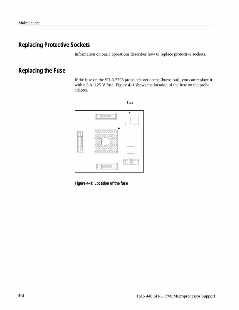
Replacing Protective SocketsInformation on basic operations describes how to replace protective sockets.
Replacing the FuseIf the fuse on the SH-3 7708 probe adapter opens (burns out), you can replace itwith a 5 A, 125 V fuse. Figure 4–1 shows the location of the fuse on the probeadapter.
Fuse
Figure 4–1: Location of the fuse

Replaceable Electrical Parts


TMS 440 SH-3 7708 Microprocessor Support 5–1
Replaceable Electrical Parts
This chapter contains a list of the replaceable electrical components for the TMS 440 SH-3 7708 microprocessor support.
Parts Ordering InformationReplacement parts are available through your local Tektronix field office orrepresentative.
Changes to Tektronix products are sometimes made to accommodate improvedcomponents as they become available and to give you the benefit of the latestimprovements. Therefore, when ordering parts, it is important to include thefollowing information in your order:
� Part number
� Instrument type or model number
� Instrument serial number
� Instrument modification number, if applicable
If you order a part that has been replaced with a different or improved part, yourlocal Tektronix field office or representative will contact you concerning anychange in part number.
Change information, if any, is located at the rear of this manual.
Using the Replaceable Electrical Parts ListThe tabular information in the Replaceable Electrical Parts List is arranged forquick retrieval. Understanding the structure and features of the list will help youfind all of the information you need for ordering replacement parts. Thefollowing table describes each column of the electrical parts list.

Replaceable Electrical Parts
5–2 TMS 440 SH-3 7708 Microprocessor Support
Parts list column descriptions
Column Column name Description
1 Component number The component number appears on diagrams and circuit board illustrations, located in the diagramssection. Assembly numbers are clearly marked on each diagram and circuit board illustration in theDiagrams section, and on the mechanical exploded views in the Replaceable Mechanical Parts listsection. The component number is obtained by adding the assembly number prefix to the circuitnumber (see Component Number illustration following this table).
The electrical parts list is arranged by assemblies in numerical sequence (A1, with its subassembliesand parts, precedes A2, with its subassemblies and parts).
Chassis-mounted parts have no assembly number prefix, and they are located at the end of theelectrical parts list.
2 Tektronix part number Use this part number when ordering replacement parts from Tektronix.
3 and 4 Serial number Column three indicates the serial number at which the part was first effective. Column four indicatesthe serial number at which the part was discontinued. No entry indicates the part is good for all serialnumbers.
5 Name & description An item name is separated from the description by a colon (:). Because of space limitations, an itemname may sometimes appear as incomplete. Use the U.S. Federal Catalog handbook H6-1 forfurther item name identification.
6 Mfr. code This indicates the code number of the actual manufacturer of the part.
7 Mfr. part number This indicates the actual manufacturer’s or vendor’s part number.
Abbreviations conform to American National Standard ANSI Y1.1–1972.
Component number
A23A2R1234 A23 R1234
Assembly number Circuit number
Read: Resistor 1234 (of Subassembly 2) of Assembly 23
A2
Subassembly number(optional)
A list of assemblies is located at the beginning of the electrical parts list. Theassemblies are listed in numerical order. When a part’s complete componentnumber is known, this list will identify the assembly in which the part is located.
Chassis-mounted parts and cable assemblies are located at the end of theReplaceable Electrical Parts List.
The table titled Manufacturers Cross Index shows codes, names, and addresses ofmanufacturers or vendors of components listed in the parts list.
Abbreviations
Component Number
List of Assemblies
Chassis Parts
Mfr. Code to ManufacturerCross Index

Replaceable Electrical Parts
TMS 440 SH-3 7708 Microprocessor Support 5–3
Manufacturers cross index
Mfr.code Manufacturer Address City, state, zip code
04222 AVX/KYOCERA PO BOX 867 MYRTLE BEACH, SC 29577
00779 AMP INC. CUSTOMER SERVICE DEPTPO BOX 3608
HARRISBURG, PA 17105–3608
01KV9 MERIX CORP 1521 POPLAR LANEPO BOX 3000
FOREST GROVE, OR 97116
26742 METHODE ELECTRONICS INC BACKPLAIN DIVISION7444 WEST WILSON AVE
CHICAGO, IL 60656–4548
50434 HEWLETT PACKARD 370 W TRIMBLE ROAD SAN JOSE, CA 95131–1008
50579 SIEMENS COMPONENTS INC OPTOELECTRONICS DIVISION1900 HOMESTEAD RD
CUPERTINO, CA 95014
56845 DALE ELECTRONIC COMPONENTS 2300 RIVERSIDE BLVDPO BOX 74
NORFOLK, NE 68701
59124 KOA SPEER ELECTRONICS INC BOLIVAR DRIVEPO BOX 547
BRADFORD, PA 16701
60381 PRECISION INTERCONNECT CORP. 16640 SW 72ND AVE PORTLAND, OR 97224
61857 SAN–O INDUSTRIAL CORP 91–3 COLIN DRIVE HOLBROOK, NY 11741
63058 BERG ELECTRONICS INC. MCKENZIE SOCKET DIV910 PAGE AVE
FREMONT, CA 94538–7340
80009 TEKTRONIX INC 14150 SW KARL BRAUN DRPO BOX 500
BEAVERTON, OR 97077–0001
85480 BRADY USA NAMEPLATE DIVISIONP O BOX 571346 ELIZABETH BRADY RD
HILLSBOROUGH, NC 27278
TK0198 HAMILTON HALLMARK 9750 SW NIMBUS AVE BEAVERTON, OR 97005
TK0875 MATSUO ELECTRONICS 2134 MAIN STREETSUITE 200
HUNTINGTON BEACH, CA 92648
TK2449 SINGATRON ENTERPRISE CO LTD 13925 MAGNOLIA AVE CHINO, CA 91710

Replaceable Electrical Parts
5–4 TMS 440 SH-3 7708 Microprocessor Support
Replaceable electrical parts list
Componentnumber
Tektronixpart number
Serial no.effective
Serial no.discont’d Name & description
Mfr.code Mfr. part number
671–4406–00 CIRCUIT BD ASSY:PQFP–144 PINS,SOLDERED,679–4406–00TESTED,389–2579–00 WIRED,TMS440 OPT 02
80009 671–4406–00
105–1089–00 LATCH ASSY:LATCH HOUSING ASSY,VERTICAL MOUNT,0.48 H X1.24 L,W/PCB SINGLE CLIP,P6434
60381 105–1089–00
131–4356–00 CONN,SHUNT:SHUNT/SHORTING,FEMALE,1 X 2,0.1 CTR,0.63H,BLK,W/HANDLE,JUMPER,
26742 9618–302–50
131–4530–00 CONN,HDR:PCB,MALE,STR,1 X 3,0.1 CTR,0.230 MLG X 0.120TAIL,30 GOLD,BD RETENTION,
00779 104344–1
131–5527–00 JACK,POWER DC:PCB,MALE,RTANG,2MM PIN,11MM H(0.433) X3.5MM(0.137) TAIL,9MM(0.354) W,TIN,W/SWI
TK2449 DJ–005–A
131–6134–01 CONN,PLUG:SMD,MICTOR,PCB,FEMALE,STR,38 POS,0.025CTR,0.245 H,GOLD,TLA7QS
00779 767004–1
136–1324–00 SOCKET,PGA:PCB,FEMALE,144 POS,12 X 12,OPENCENTER,SHORT PINS,PGA–144H101B1–1302–R
63058 PGA–144H101B1–1302–R
136–1325–00 SOCKET,PGA:PCB,FEMALE,STR,144 POS,12 X 12,LONGPINS,VENDOR NUMBER,PGA–144H115B1–1302–R
63058 PGA–144H115B1–1302–R
150–5001–00 DIODE,OPTO:LED,GRN,565NM,2.0VF AT 10MA IF,12.5VFMAX,0.4MCD MIN AT 10MA,LG S260–DO,SOT–23,
50579 LGS260–DOGEGURT
152–5045–00 DIODE,SIG:SCHOTTKY,20V,1.2PF,24OHM,HSMS–2810,TO–236/SOT–23,8MM T&R
50434 HSMS–2810–T31
159–0059–00 FUSE,WIRE LEAD:5A,125V 61857 SPI–5A
163–1106–00 IC,DIGITAL:PRGM156–7407–00,CMOS,PLD,EEPLD,22V10,140MA,5NS,PAL1,22V10–5,PLCC28–1,TUBE
TK0198 163–1106–00
163–1107–00 IC,DIGITAL:PRGM156–7407–00,CMOS,PLD,EEPLD,22V10,140MA,5NS,PAL2,22V10,PLCC28–1,TUBE
TK0198 163–1107–00
283–5114–00 CAP,FXD,CERAMIC;MLC;0.1UF,10%,50V,X7R,1206;SMD,8MMT&R
04222 12065C104KAT(1AOR 3A)
290–5005–00 CAP,FXD,TANT:47UF,10%,10V,5.8MM X 4.6MM,5846,SMD,T&R TK0875 267M–1002–476–KR–533
307–5131–00 RES,NTWK,FXD,FI:(4) 180 OHM,5%,63MWEACH,50V,200PPM,ISOLATED,ARRAY,SMD,T&R
56845 CRA06S0803–181J–RT1
321–5454–00 RES,FXD,FILM:332 OHM,1%,50V,62.5MW,0603,SMD,T&R 59124 RK73H1J3320FT

Diagrams


6–1TMS 440 SH-3 7708 Microprocessor Support
Diagrams and Circuit Board Illustrations
This section contains the troubleshooting procedures, block diagrams, circuit boardillustrations, component locator tables, waveform illustrations, and schematic diagrams.
SymbolsGraphic symbols and class designation letters are based on ANSI Standard Y32.2-1975.Abbreviations are based on ANSI Y1.1-1972.
Logic symbology is based on ANSI/IEEE Standard 91-1984 in terms of positive logic.Logic symbols depict the logic function performed and can differ from the manufacturer’sdata.
The tilde (~) preceding a signal name indicates that the signal performs its intendedfunction when in the low state.
Other standards used in the preparation of diagrams by Tektronix, Inc., include thefollowing:
� Tektronix Standard 062-2476 Symbols and Practices for Schematic Drafting
� ANSI Y14.159-1971 Interconnection Diagrams
� ANSI Y32.16-1975 Reference Designations for Electronic Equipment
� MIL-HDBK-63038-1A Military Standard Technical Manual Writing Handbook
Component ValuesElectrical components shown on the diagrams are in the following units unless notedotherwise:
Capacitors: Values one or greater are in picofarads (pF).Values less than one are in microfarads (�F).
Resistors: Values are in Ohms (�).
Graphic Items and Special Symbols Used in This ManualEach assembly in the instrument is assigned an assembly number (for example A5). Theassembly number appears in the title on the diagram, in the lookup table for the schematicdiagram, and corresponding component locator illustration. The Replaceable ElectricalParts list is arranged by assembly in numerical sequence; the components are listed bycomponent number.
Locator GridFunction Block Title
Internal Screw Adjustment
Onboard JumperDigital Ground
Refer to Assembly& Diagram Number
Offboard ConnectorActive Low Signal
Signal FromAnother Diagram,
Same Board
Power Termination
Strap
Panel Control
Female CoaxialConnector
Heat SinkDecoupled VoltageDiagram Number
Diagram Name
��� ����� � ��
Component on back of board
Assembly Number
A
B
1 2 3 4
��� ����
Component Locator DiagramsThe schematic diagram and circuit board component location illustrations have gridsmarked on them. The component lookup tables refer to these grids to help you locate acomponent. The circuit board illustration appears only once; its lookup table lists thediagram number of all diagrams on which the circuitry appears.
Some of the circuit board component location illustrations are expanded and divided intoseveral parts to make it easier for you to locate small components. To determine whichpart of the whole locator diagram you are looking at, refer to the small locator key shownbelow. The gray block, within the larger circuit board outline, shows where that part fitsin the whole locator diagram. Each part in the key is labeled with an identifying letter thatappears in the figure titles under component locator diagrams.
� �
��
Section of CircuitBoard Shown

6–2 TMS 440 SH-3 7708 Microprocessor Support

TMS 440 SH-3 7708 Microprocessor Support


TMS 440 SH-3 7708 Microprocessor Support
180 180 180
VCC = +5VVDD = User VCCGND1 = GNDGND2 = GNDGND3 = GNDGND4 = GND


Replaceable Mechanical Parts


TMS 440 SH-3 7708 Microprocessor Support 7–1
Replaceable Mechanical Parts
This chapter contains a list of the replaceable mechanical components for theTMS 440 SH-3 7708 microprocessor support.
Parts Ordering InformationReplacement parts are available through your local Tektronix field office orrepresentative.
Changes to Tektronix products are sometimes made to accommodate improvedcomponents as they become available and to give you the benefit of the latestimprovements. Therefore, when ordering parts, it is important to include thefollowing information in your order:
� Part number
� Instrument type or model number
� Instrument serial number
� Instrument modification number, if applicable
If you order a part that has been replaced with a different or improved part, yourlocal Tektronix field office or representative will contact you concerning anychange in part number.
Change information, if any, is located at the rear of this manual.
Using the Replaceable Mechanical Parts ListThe tabular information in the Replaceable Mechanical Parts List is arranged forquick retrieval. Understanding the structure and features of the list will help youfind all of the information you need for ordering replacement parts. Thefollowing table describes the content of each column in the parts list.

Replaceable Mechanical Parts
7–2 TMS 440 SH-3 7708 Microprocessor Support
Parts list column descriptions
Column Column name Description
1 Figure & index number Items in this section are referenced by figure and index numbers to the exploded view illustrationsthat follow.
2 Tektronix part number Use this part number when ordering replacement parts from Tektronix.
3 and 4 Serial number Column three indicates the serial number at which the part was first effective. Column fourindicates the serial number at which the part was discontinued. No entries indicates the part isgood for all serial numbers.
5 Qty This indicates the quantity of parts used.
6 Name & description An item name is separated from the description by a colon (:). Because of space limitations, anitem name may sometimes appear as incomplete. Use the U.S. Federal Catalog handbook H6-1for further item name identification.
7 Mfr. code This indicates the code of the actual manufacturer of the part.
8 Mfr. part number This indicates the actual manufacturer’s or vendor’s part number.
Abbreviations conform to American National Standard ANSI Y1.1–1972.
Chassis-mounted parts and cable assemblies are located at the end of theReplaceable Electrical Parts List.
The table titled Manufacturers Cross Index shows codes, names, and addresses ofmanufacturers or vendors of components listed in the parts list.
Abbreviations
Chassis Parts
Mfr. Code to ManufacturerCross Index

Replaceable Mechanical Parts
TMS 440 SH-3 7708 Microprocessor Support 7–3
Manufacturers cross index
Mfr.code Manufacturer Address City, state, zip code
00779 AMP INC. CUSTOMER SERVICE DEPTPO BOX 3608
HARRISBURG, PA 17105–3608
05276 ITT POMONA ELECTRONICS 1500 E NINTH ST POMONA, CA 91766–3835
0KB05 NORTH STAR NAMEPLATE INC 5750 NE MOORE COURT HILLSBORO, OR 97124–6474
14310 AULT INC 7300 BOONE AVE NORTHBROOKLINE PARK
MINNEAPOLIS, MN 55428
26742 METHODE ELECTRONICS INC BACKPLAIN DIVISION7444 WEST WILSON AVE
CHICAGO, IL 60656–4548
60381 PRECISION INTERCONNECT CORP. 16640 SW 72ND AVE PORTLAND, OR 97224
61857 SAN–O INDUSTRIAL CORP 91–3 COLIN DRIVE HOLBROOK, NY 11741
63058 BERG ELECTRONICS INC. MCKENZIE SOCKET DIV910 PAGE AVE
FREMONT, CA 94538–7340
80009 TEKTRONIX INC 14150 SW KARL BRAUN DRPO BOX 500
BEAVERTON, OR 97077–0001
S3109 FELLER U.S. CORPORATION 72 VERONICA AVEUNIT #4
SOMERSET, NJ 08873
TK1943 NEILSEN MANUFACTURING INC 3501 PORTLAND RD NE SALEM, OR 97303
TK2449 SINGATRON ENTERPRISE CO LTD 13925 MAGNOLIA AVE CHINO, CA 91710
TK2548 XEROX CORPORATION 14181 SW MILLIKAN WAY BEAVERTON, OR 97005

Replaceable Mechanical Parts
7–4 TMS 440 SH-3 7708 Microprocessor Support
Replaceable mechanical parts list
Fig. &indexnumber
Tektronix partnumber
Serial no.effective
Serial no.discont’d Qty Name & description
Mfr.code Mfr. part number
5–1–0 010–0621–00 1 ADAPTER,PROBE:SH7708,PQFP–144 PINS, PROBEADAPTER,TMS440 OPT 02
80009 010–0621–00
–1 671–4406–00 1 CIRCUIT BD ASSY:PQFP–144 PINS,SOLDERED,679–4406–00TESTED,389–2579–00 WIRED,TMS440 OPT 02
80009 671–4406–00
–2 131–6134–01 3 CONN,RCPT:SMD,MICTOR,FEMALE,STR,38 POS,0.025CTR,0.240 H,W/0.108 PCB HOLD DOWNS.PALLADIUM
00779 767054–1
–3 105–1089–00 3 LATCH ASSY:LATCH HOUSING ASSY,VERTICAL MOUNT,0.48H X 1.24 L,W/PCB SINGLE CLIP,P6434
60381 105–1089–00
–4 131–4356–00 6 CONN,SHUNT:SHUNT/SHORTING,FEMALE,1 X 2,0.1 CTR,0.63H,BLK,W/HANDLE,JUMPER,
26742 9618–302–50
–5 131–4530–00 6 CONN,HDR:PCB,MALE,STR,1X3,0.1 CTR,0.230 MLG X 0.120TAIL, 30 GOLD, BD RETENTION
00779 104344–1
–6 131–5527–00 1 JACK,POWER DC:PCB,MALE,RTANG,2MM PIN,11MMH(0.433) X 3.5MM(0.137) TAIL,9MM(0.354) W,TIN,W/SWI
TK2449 DJ–005–A
–7 159–0059–00 1 FUSE,WIRE LEAD:5A,125V 61857 SPI–5A
–8 136–1324–00 2 SOCKET,PGA:PCB,FEMALE,144 POS,12 X 12,OPENCENTER,SHORT PINS,PGA–144H101B1–1302–R
63058 PGA–144H101B1–1302–R
–9 103–0415–00 1 ADAPTER,PQFP:TEST CLIP,144,PQFP–144(6151),TMS440 02 05276 6151
STANDARD ACCESSORIES
071–0153–00 1 MANUAL,TECH INSTRUCTIONS,SH 7708;TMS440 80009 071–0153–00
070–9803–00 1 MANUAL,TECH;TLA 700 SERIES MICRO SUPPORTINSTALLATION
80009 070–9803–00
161–0104–00 1 CA ASSY,PWR:3,18 AWG,98 L,250V/10AMP,98INCH,RTANG,IEC320,RCPT X STR,NEMA 15–5P,W/CORDGRIP,
S3109 ORDER BYDESCRIPTION
119–5061–01 1 POWER SUPPLY:25W,5V 5A,CONCENTRIC2MM,90–265V,47–63 HZ IEC,15X8.6X5 CM, UL,CSA,TUV,IEC,SELF
14310 SW108KA0002F01
OPTIONAL ACCESSORIES
P6434 * 3 P6434 MASS TERMINATION PROBE 80009 ORDER BY DESCRIPTION
161–0104–05 1 CA ASSY,PWR:3,1.0MM SQ,250V/10A,2.5 ME-TER,RTANG,IEC320,RCPT,AUSTRALIA,SAFTEY CON-TROLLED (OPT A3)
S3109 ORDER BYDESCRIPTION
161–0104–06 1 CA ASSY,PWR:3,1.0MM SQ 250V/10A,2.5 ME-TER,RTANG,IEC320,RCPT, EUROPEAN,SAFTEY CON-TROLLED(OPT A1)
S3109 ORDER BYDESCRIPTION
161–0104–07 1 CA ASSY,PWR:1.0MM SQ 250V/10A,2.5 ME-TER,RTANG,IEC320,RCPT X 13A,FUSED,UK PLUG,(13AFUSE),UNITED KINGDOM,SAFTEY CONTROL(OPT A2)
S3109 ORDER BYDESCRIPTION
161–0167–00 1 CA ASSY,PWR:3,0.75MM SQ 250V/10A,2.5 ME-TER,RTANG,IEC320,RCPT,SWISS,SAFTEY CON-TROLLED(OPT A5)
S3109 ORDER BYDESCRIPTION
* Check the P6434 manual for detailed replaceable part number information.

Replaceable Mechanical Parts
TMS 440 SH-3 7708 Microprocessor Support 7–5
1
2
3
4
5
6
7
8
9
Figure 7–1: SH-3 7708 probe adapter exploded view

Replaceable Mechanical Parts
7–6 TMS 440 SH-3 7708 Microprocessor Support

Index


TMS 440 SH-3 7708 Microprocessor Support Index–1
IndexAabout this manual set, ixacquiring data, 2–11acquisition clocking, 2–2Address group, channel assignments, 1–11Alternate bus master, 1–3application, logic analyzer configuration, 1–2
Bbasic operations, where to find information, ixBig-Endian byte order, 2–15bus cycles, displayed cycle types, 2–12Bus Widths (CS0 – CS6), 2–15Byte Order, 2–15
Ccache invalidation, 1–3channel assignments
Address group, 1–11clocks, 1–14, 1–15Control group, 1–13Data group, 1–12signals not acquired, 1–16
channel groups, 2–1visibility, 2–11
clock channel assignments, 1–14, 1–15, 1–16clock rate, 1–2
SUT, 3–1clocking, Custom, 2–1
how data is acquired, 2–1component locator diagrams, 6–1connections
CPU to Mictor, 1–16no probe adapter, 1–8
channel probes, 1–9probe adapter to SUT, QFP, 1–4
contacting Tektronix, xControl Flow display format, 2–13Control group
channel assignments, 1–13symbol table, 2–9
Control signals, 2–1CPU to Mictor connections, 1–16Custom Clocking, 2–1
acquisition clocking, 2–2DRAM access, 2–4
EDO DRAM, 2–5Memory Type, 2–2PSRAM Access, 2–7SDRAM Mode Register Accesses, 2–8SDRAM Read, 2–5SRAM/ROM/PCMIA acess, 2–3
Custom clocking, 2–1how data is acquired, 2–1
cycle types, 2–12
Ddata
acquiring, 2–11disassembly formats
Control Flow, 2–13Hardware, 2–12Software, 2–13Subroutine, 2–14
data display, changing, 2–14Data group, channel assignments, 1–12definitions
disassembler, ixHI module, xinformation on basic operations, ixLO module, xlogic analyzer, xmodule, xP54C, ixSUT, ixXXX, ix
demonstration file, 2–17diagrams and circuit board illustrations, 6–1disassembled data
change displayed data, 2–14cycle type definitions, 2–12viewing, 2–11viewing an example, 2–17
disassemblerdefinition, ixlogic analyzer configuration, 1–2setup, 2–1
Disassembly Format Definition overlay, 2–14Disassembly property page, 2–14display formats
Control Flow, 2–13Hardware, 2–12Software, 2–13special characters, 2–11

Index
Index–2 TMS 440 SH-3 7708 Microprocessor Support
Subroutine, 2–14DRAM access, 2–4
EEDO DRAM, 2–5electrical specifications, 3–1
clock rate, 3–1loading, 3–1
environmental specifications, 3–3exception vectors, 2–17
Ffuse, replacing, 4–2
HHardware display format, 2–12
cycle type definitions, 2–12HI module, definition, xhold time, minimum, 3–1
Iinspection and cleaning
microcontroller, 1–6QFP test clip, 1–6
installing hardware. See connections
Lleads (podlets). See connectionsLittle-Endian byte order, 2–15LO module, definition, xloading, 3–1
signal, 3–1logic analyzer
configuration for disassembler, 1–2configuration for the application, 1–2definition, xsoftware compatibility, 1–2
Mmanual
conventions, ixhow to use the set, ix
Mark Cycle function, 2–16Mark Opcode function, 2–16
marking cycles, definition of, 2–16MCR, 2–16Memory Type, 2–2
Area 2, 2–16Area 3, 2–16
memory types, Control signals, 2–1microprocessor, specific clocking and how data is
acquired, 2–1Mictor to CPU connections, 1–16MMU Address, 2–15module, definition, x
OOptional Display Selections
AMX Bits in MCR, 2–16Bus Widths (CS0 – CS6), 2–15Byte Order, 2–15Memory Type
Area 2, 2–16Area 3, 2–16
MMU, 2–15VBR, 2–14
PP54C, definition, ixP6434 probes, labeling, 1–2power
for the probe adapterapplying, 1–9removing, 1–10
SUT, 1–3power adapter, 1–9power jack, 1–9power requirements
probe adapter, 3–1SUT, 3–1
Prefetch Byte Ord field, 2–15probe adapter
circuit description, 4–1clearance, 1–4configuring, 1–4connecting leads, 1–5hardware description, 4–1how to unlock test clip, 1–8inspection and cleaning, 1–6not using one, 1–8removing, 1–8replacing the fuse, 4–2
PSRAM Access, 2–7

Index
TMS 440 SH-3 7708 Microprocessor Support Index–3
QQFP test clip, inspection and cleaning, 1–6
Rreference memory, 2–17restrictions, 1–2
without a probe adapter, 1–8
SSDRAM Mode Register Accesses, 2–8SDRAM Read, 2–5service information, 4–1set up time, minimum, 3–1setups
disassembler, 2–1support, 2–1
signal loading, 3–1signals, active low sign, xSoftware display format, 2–13special characters displayed, 2–11specifications, 3–1
channel assignments, 1–10electrical, 3–1environmental, 3–3
SRAM/ROM/PCMCIA access, 2–3
Subroutine display format, 2–14support, setup, 2–1support setup, 2–1SUT, definition, ixSUT power, 1–3symbol table, Control channel group, 2–9system file, demonstration, 2–17
TTektronix, how to contact, xterminology, ixtest clip
how to lock, 1–7how to unlock, 1–8inspection and cleaning, 1–6removing, 1–8
typical signal loading, 3–1
VVBR, 2–14viewing disassembled data, 2–11
XXXX, definition, ix

Index
Index–4 TMS 440 SH-3 7708 Microprocessor Support