
TLV1117LV 1-A, Positive Fixed-Voltage, Low-Dropout … accuracy. A very high power-supply rejection...
24
INPUT OUTPUT GND Device CIN 1 μF COUT 1 μF Product Folder Sample & Buy Technical Documents Tools & Software Support & Community TLV1117LV SBVS160B – MAY 2011 – REVISED FEBRUARY 2015 TLV1117LV 1-A, Positive Fixed-Voltage, Low-Dropout Regulator 1 Features 3 Description The TLV1117LV series of low-dropout (LDO) linear 1• 1.5% Typical Accuracy regulators is a low input voltage version of the • Low I Q : 100 μA (Maximum) popular TLV1117 voltage regulator. – 500 Times Lower Than Standard 1117 The TLV1117LV is an extremely low-power device Devices that consumes 500 times lower quiescent current • V IN : 2 V to 5.5 V than traditional 1117 voltage regulators, making the device suitable for applications that mandate very low – Absolute Maximum V IN =6V standby current. The TLV1117LV family of LDOs is • Stable With 0-mA Output Current also stable with 0 mA of load current; there is no • Low Dropout: 455 mV at 1 A for V OUT = 3.3 V minimum load requirement, making the device an • High PSRR: 65 dB at 1 kHz ideal choice for applications where the regulator must power very small loads during standby in addition to • Minimum Ensured Current Limit: 1.1 A large currents on the order of 1 A during normal • Stable With Cost-Effective Ceramic Capacitors: operation. The TLV1117LV offers excellent line and – With 0-Ω ESR load transient performance, resulting in very small magnitude undershoots and overshoots of output • Temperature Range: –40°C to 125°C voltage when the load current requirement changes • Thermal Shutdown and Overcurrent Protection from less than 1 mA to more than 500 mA. • Available in SOT-223 Package A precision bandgap and error amplifier provides – See Mechanical, Packaging, and Orderable 1.5% accuracy. A very high power-supply rejection Information at the end of this document for a ratio (PSRR) enables use of the device for post- complete list of available voltage options. regulation after a switching regulator. Other valuable features include low output noise and low-dropout 2 Applications voltage. • Set Top Boxes The device is internally compensated to be stable with 0-Ω equivalent series resistance (ESR) • TVs and Monitors capacitors. These key advantages enable the use of • PC Peripherals, Notebooks, Motherboards cost-effective, small-size ceramic capacitors. Cost- • Modems and Other Communication Products effective capacitors that have higher bias voltages • Switching Power Supply Post-Regulation and temperature derating can also be used if desired. The TLV1117LV series is available in a SOT-223 package. Device Information (1) PART NUMBER PACKAGE BODY SIZE (NOM) TLV1117LV SOT-223 (4) 6.50 mm x 3.50 mm (1) For all available packages, see the orderable addendum at the end of the data sheet. Typical Application Circuit 1 An IMPORTANT NOTICE at the end of this data sheet addresses availability, warranty, changes, use in safety-critical applications, intellectual property matters and other important disclaimers. PRODUCTION DATA.
Transcript of TLV1117LV 1-A, Positive Fixed-Voltage, Low-Dropout … accuracy. A very high power-supply rejection...
INPUT OUTPUT
GND
DeviceCIN
1 µFCOUT
1 µF
Product
Folder
Sample &Buy
Technical
Documents
Tools &
Software
Support &Community
TLV1117LVSBVS160B –MAY 2011–REVISED FEBRUARY 2015
TLV1117LV 1-A, Positive Fixed-Voltage, Low-Dropout Regulator1 Features 3 Description
The TLV1117LV series of low-dropout (LDO) linear1• 1.5% Typical Accuracy
regulators is a low input voltage version of the• Low IQ: 100 μA (Maximum) popular TLV1117 voltage regulator.– 500 Times Lower Than Standard 1117
The TLV1117LV is an extremely low-power deviceDevices that consumes 500 times lower quiescent current• VIN: 2 V to 5.5 V than traditional 1117 voltage regulators, making the
device suitable for applications that mandate very low– Absolute Maximum VIN = 6 Vstandby current. The TLV1117LV family of LDOs is• Stable With 0-mA Output Currentalso stable with 0 mA of load current; there is no
• Low Dropout: 455 mV at 1 A for VOUT = 3.3 V minimum load requirement, making the device an• High PSRR: 65 dB at 1 kHz ideal choice for applications where the regulator must
power very small loads during standby in addition to• Minimum Ensured Current Limit: 1.1 Alarge currents on the order of 1 A during normal• Stable With Cost-Effective Ceramic Capacitors: operation. The TLV1117LV offers excellent line and
– With 0-Ω ESR load transient performance, resulting in very smallmagnitude undershoots and overshoots of output• Temperature Range: –40°C to 125°Cvoltage when the load current requirement changes• Thermal Shutdown and Overcurrent Protectionfrom less than 1 mA to more than 500 mA.
• Available in SOT-223 PackageA precision bandgap and error amplifier provides– See Mechanical, Packaging, and Orderable 1.5% accuracy. A very high power-supply rejectionInformation at the end of this document for a ratio (PSRR) enables use of the device for post-
complete list of available voltage options. regulation after a switching regulator. Other valuablefeatures include low output noise and low-dropout
2 Applications voltage.• Set Top Boxes The device is internally compensated to be stable
with 0-Ω equivalent series resistance (ESR)• TVs and Monitorscapacitors. These key advantages enable the use of• PC Peripherals, Notebooks, Motherboardscost-effective, small-size ceramic capacitors. Cost-• Modems and Other Communication Products effective capacitors that have higher bias voltages
• Switching Power Supply Post-Regulation and temperature derating can also be used if desired.
The TLV1117LV series is available in a SOT-223package.
Device Information(1)
PART NUMBER PACKAGE BODY SIZE (NOM)TLV1117LV SOT-223 (4) 6.50 mm x 3.50 mm
(1) For all available packages, see the orderable addendum atthe end of the data sheet.
Typical Application Circuit
1
An IMPORTANT NOTICE at the end of this data sheet addresses availability, warranty, changes, use in safety-critical applications,intellectual property matters and other important disclaimers. PRODUCTION DATA.

TLV1117LVSBVS160B –MAY 2011–REVISED FEBRUARY 2015 www.ti.com
Table of Contents8.1 Application Information .......................................... 131 Features .................................................................. 18.2 Typical Application .................................................. 132 Applications ........................................................... 18.3 Do's and Don'ts....................................................... 143 Description ............................................................. 1
9 Power Supply Recommendations ...................... 144 Revision History..................................................... 210 Layout................................................................... 155 Pin Configuration and Functions ......................... 3
10.1 Layout Guidelines ................................................. 156 Specifications......................................................... 410.2 Layout Example .................................................... 156.1 Absolute Maximum Ratings ..................................... 410.3 Thermal Protection................................................ 156.2 ESD Ratings ............................................................ 410.4 Power Dissipation ................................................. 156.3 Recommended Operating Conditions....................... 4
11 Device and Documentation Support ................. 166.4 Thermal Information .................................................. 411.1 Device Support...................................................... 166.5 Electrical Characteristics........................................... 511.2 Documentation Support ........................................ 166.6 Typical Characteristics .............................................. 611.3 Related Links ........................................................ 167 Detailed Description ............................................ 1111.4 Trademarks ........................................................... 167.1 Overview ................................................................. 1111.5 Electrostatic Discharge Caution............................ 167.2 Functional Block Diagram ....................................... 1111.6 Glossary ................................................................ 177.3 Feature Description................................................. 11
12 Mechanical, Packaging, and Orderable7.4 Device Functional Modes........................................ 12Information ........................................................... 178 Application and Implementation ........................ 13
4 Revision HistoryNOTE: Page numbers for previous revisions may differ from page numbers in the current version.
Changes from Revision A (September 2011) to Revision B Page
• Added ESD Ratings table, Feature Description section, Device Functional Modes, Application and Implementationsection, Power Supply Recommendations section, Layout section, Device and Documentation Support section, andMechanical, Packaging, and Orderable Information section ................................................................................................. 1
• Replaced front-page figure .................................................................................................................................................... 1• Deleted Dissipation Ratings table........................................................................................................................................... 4
Changes from Original (May, 2011) to Revision A Page
• Changed front-page figure ..................................................................................................................................................... 1
2 Submit Documentation Feedback Copyright © 2011–2015, Texas Instruments Incorporated
Product Folder Links: TLV1117LV

INPUT
GND
2
3
1
OUTPUT
OU
TP
UT
TLV1117LVwww.ti.com SBVS160B –MAY 2011–REVISED FEBRUARY 2015
5 Pin Configuration and Functions
DCY Package4 Pins (SOT-223)
Top View
Pin FunctionsPIN
I/O DESCRIPTIONNAME NO.
Input pin. See Input and Output Capacitor Requirements in the Application and ImplementationIN 3 I section for more details.OUT 2, Tab O Regulated output voltage pin. See Input and Output Capacitor Requirements for more details.GND 1 — Ground pin.
Copyright © 2011–2015, Texas Instruments Incorporated Submit Documentation Feedback 3
Product Folder Links: TLV1117LV
TLV1117LVSBVS160B –MAY 2011–REVISED FEBRUARY 2015 www.ti.com
6 Specifications
6.1 Absolute Maximum RatingsAt TJ = 25°C (unless otherwise noted). All voltages are with respect to GND. (1)
MIN MAX UNITVIN –0.3 6 V
VoltageVOUT –0.3 6 V
Current IOUT Internally limitedOutput short-circuit duration IndefiniteContinuous total power PDISS See Thermal Informationdissipation
Operating junction, TJ –55 150 °CTemperature
Storage, Tstg –55 150 °C
(1) Stresses beyond those listed under Absolute Maximum Ratings may cause permanent damage to the device. These are stress ratingsonly, and functional operation of the device at these or any other conditions beyond those indicated under Recommended OperatingConditions is not implied. Exposure to absolute-maximum-rated conditions for extended periods my affect device reliability.
6.2 ESD RatingsVALUE UNIT
Human body model (HBM), per ANSI/ESDA/JEDEC JS-001, ±2000all pins (1)V(ESD) Electrostatic discharge V
Charged device model (CDM), per JEDEC specification ±500JESD22-C101, all pins (2)
(1) JEDEC document JEP155 states that 500-V HBM allows safe manufacturing with a standard ESD control process.(2) JEDEC document JEP157 states that 250-V CDM allows safe manufacturing with a standard ESD control process.
6.3 Recommended Operating Conditionsover operating free-air temperature range (unless otherwise noted)
MIN NOM MAX UNITVIN 2 5.5 VVOUT 0 5.5 VIOUT 0 1 A
6.4 Thermal InformationTLV1117LV
THERMAL METRIC (1) DCY (SOT-223) UNIT4 PINS
RθJA Junction-to-ambient thermal resistance 62.9θJCtop Junction-to-case (top) thermal resistance 47.2RθJC(top) Junction-to-board thermal resistance 12 °C/WψJT Junction-to-top characterization parameter 6.1ψJB Junction-to-board characterization parameter 11.9
(1) For more information about traditional and new thermal metrics, see the IC Package Thermal Metrics application report, SPRA953.
4 Submit Documentation Feedback Copyright © 2011–2015, Texas Instruments Incorporated
Product Folder Links: TLV1117LV
TLV1117LVwww.ti.com SBVS160B –MAY 2011–REVISED FEBRUARY 2015
6.5 Electrical CharacteristicsAt VIN = VOUT(nom) + 1.5 V; IOUT = 10 mA, COUT = 1.0 μF, and TA = 25°C, unless otherwise noted.
PARAMETER TEST CONDITIONS MIN TYP MAX UNITVIN Input voltage range 2 5.5 V
VOUT > 2 V –1.5% 1.5%DC outputVOUT 1.5 V ≤ VOUT < 2 V –2% 2%accuracy
1.2 V ≤ VOUT < 1.5 V –40 40 mVΔVOUT(ΔVIN) Line regulation VOUT(nom) + 0.5 V ≤ VIN ≤ 5.5 V, IOUT = 10 mA 1 5 mVΔVOUT(ΔIOUT) Load regulation 0 mA ≤ IOUT ≤ 1 A 1 35 mV
IOUT = 200 mA 115 mVIOUT = 500 mA 285 mV
VOUT < 3.3 VIOUT = 800 mA 455 mVIOUT = 1 A 570 800 mVVIN = 0.98 xVDO Dropout voltage (1)
VOUT(nom) IOUT = 200 mA 90 mVIOUT = 500 mA 230 mV
VOUT ≥ 3.3 VIOUT = 800 mA 365 mVIOUT = 1 A 455 700 mV
ICL Output current limit VOUT = 0.9 × VOUT(nom) 1.1 AIQ Quiescent current IOUT = 0 mA 50 100 µA
Power-supply VIN = 3.3 V, VOUT = 1.8 V,PSRR 65 dBrejection ratio IOUT = 500 mA, f = 100 HzOutput noise BW = 10 Hz to 100 kHz, VIN = 2.8 V, VOUT = 1.8 V,Vn 60 µVRMSvoltage IOUT = 500 mA
tSTR Startup time (2) COUT = 1.0 µF, IOUT = 1 A 100 µsUndervoltageUVLO VIN rising 1.95 Vlockout
Shutdown, temperature increasing 165 °CThermal shutdownTSD temperature Reset, temperature decreasing 145 °COperating junctionTJ –40 125 °Ctemperature
(1) VDO is measured for devices with VOUT(nom) = 2.5 V so that VIN = 2.45 V.(2) Startup time = time from when VIN asserts to when output is sustained at a value greater than or equal to 0.98 × VOUT(nom).
Copyright © 2011–2015, Texas Instruments Incorporated Submit Documentation Feedback 5
Product Folder Links: TLV1117LV

600
500
400
300
200
100
0
Dro
pout V
oltage (
mV
)
0 100 200 300 400 500 600 700 800 900 1000
Output Current (mA)
+125 C
+85 C
+25 C
40 C-
°
°
°
°
-40 -25 -10 5 20 35 65 95 125
Temperature ( )C°
1.9
1.85
1.8
1.75
1.7
Outp
ut V
oltage (
V)
V = 1.8 VOUT
50 80 110
10 mA
500 mA
2 2.5 3 3.5 4 4.5
1200
1000
800
600
400
200
0
Dro
po
ut
Vo
lta
ge
(m
V)
Input Voltage (V)
+85 C
+25 C
40 C-
°
°
°
0 100 200 300 400 500 600 700 1000
Output Current (mA)
1.9
1.85
1.8
1.75
1.7
Ou
tpu
t V
olta
ge
(V
)
+125 C
+85 C
+25 C
40 C-
°
°
°
°
800 900
V = 1.8 VOUT
2.3 2.7 3.1 3.5 3.9 4.3 4.7 5.1 5.5
Input Voltage (V)
1.9
1.85
1.8
1.75
1.7
Ou
tpu
t V
olta
ge
(V
)
+125 C
+85 C
+25 C
40 C-
°
°
°
°
V = 1.8 V
I = 10 mAOUT
OUT
3.3 3.5 3.7 3.9 4.1 4.3 4.7 5.1 5.5
Input Voltage (V)
1.9
1.85
1.8
1.75
1.7
Ou
tpu
t V
olta
ge
(V
)
+85 C
+25 C
40 C-
°
°
°
V = 1.8 V
I = 1 AOUT
OUT
4.5 4.9 5.3
TLV1117LVSBVS160B –MAY 2011–REVISED FEBRUARY 2015 www.ti.com
6.6 Typical CharacteristicsAt VIN = VOUT(nom) + 1.5 V; IOUT = 10 mA, COUT = 1.0 μF, and TA = 25°C, unless otherwise noted.
Figure 1. Line Regulation Figure 2. Line Regulation
Figure 3. Load Regulation Figure 4. Dropout Voltage vs Input
Figure 5. Dropout Voltage vs Output Figure 6. Output Voltage vs Temperature
6 Submit Documentation Feedback Copyright © 2011–2015, Texas Instruments Incorporated
Product Folder Links: TLV1117LV
10
1
0.1
0.01
0.001
No
ise
Sp
ectr
al D
en
sity (
V/
)m
?H
z
10 100 1 k 10 k 100 k 1 M 10 M
Frequency (Hz)
0 100 200 300 400 500 600 700 800 900 1000
Output Current (mA)
90
80
70
60
50
40
30
20
10
0
Po
we
r-S
up
ply
Re
jectio
n R
atio
(d
B)
V V = 1.5 V-IN OUT
f = 120 Hzf = 50 Hz
f = 10 kHz
f = 10 MHz
f = 1 kHzf = 100 kHz
f = 1 MHz
10 100 1 k 100 k 1 M 10 M
Frequency (Hz)
90
80
70
60
50
40
30
20
10
0
Pow
er-
Supply
Reje
ction R
atio (
dB
)
10 k
V V = 3 V-IN OUT
I = 500 mA
I = 150 mA
I = 30 mA
OUT
OUT
OUT
10 100 1 k 100 k 1 M 10 M
Frequency (Hz)
90
80
70
60
50
40
30
20
10
0
Pow
er-
Supply
Reje
ction R
atio (
dB
)
10 k
V V = 1.5 V-IN OUT
I = 500 mA
I = 150 mA
I = 30 mA
OUT
OUT
OUT
600
500
400
300
200
100
0
Quie
scent C
urr
ent (
A)
m
0 100 200 300 400 500 600 700 800 900 1000
Output Current (mA)
+125 C
+85 C
+25 C
40 C-
°
°
°
°
3.3 3.5 3.7 3.9 4.1 4.3 4.7 5.1 5.5
Input Voltage (V)
1.8
1.78
1.76
1.74
1.72
1.7
1.68
1.66
1.64
1.62
1.6
Cu
rre
nt
Lim
it (
mA
)
4.5 4.9 5.3
+85 C
+25 C
40 C-
°
°
°
TLV1117LVwww.ti.com SBVS160B –MAY 2011–REVISED FEBRUARY 2015
Typical Characteristics (continued)At VIN = VOUT(nom) + 1.5 V; IOUT = 10 mA, COUT = 1.0 μF, and TA = 25°C, unless otherwise noted.
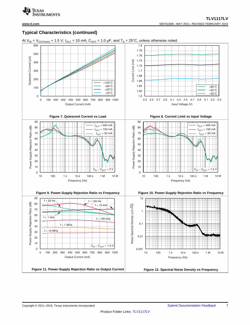
Figure 7. Quiescent Current vs Load Figure 8. Current Limit vs Input Voltage
Figure 9. Power-Supply Rejection Ratio vs Frequency Figure 10. Power-Supply Rejection Ratio vs Frequency
Figure 11. Power-Supply Rejection Ratio vs Output Current Figure 12. Spectral Noise Density vs Frequency
Copyright © 2011–2015, Texas Instruments Incorporated Submit Documentation Feedback 7
Product Folder Links: TLV1117LV
50 s/divm
100 m
V/d
iv500 m
A/d
iv
IOUT
VOUT
200 mA
1 A
50 s/divm
100 m
V/d
iv500 m
A/d
iv
IOUT
VOUT
200 mA
1 A
V = 2.8 VIN
50 s/divm
50 m
V/d
iv500 m
A/d
iv
IOUT
VOUT
1 mA
500 mA
50 s/divm
50 m
V/d
iv500 m
A/d
ivIOUT
VOUT
1 mA
500 mA
V = 2.8 VIN
50 s/divm
50 m
V/d
iv200 m
A/d
iv
IOUT
VOUT
200 mA
500 mA V = 2.8 VIN
50 s/divm
50 m
V/d
iv200 m
A/d
iv
IOUT
VOUT
200 mA
500 mA
TLV1117LVSBVS160B –MAY 2011–REVISED FEBRUARY 2015 www.ti.com
Typical Characteristics (continued)At VIN = VOUT(nom) + 1.5 V; IOUT = 10 mA, COUT = 1.0 μF, and TA = 25°C, unless otherwise noted.
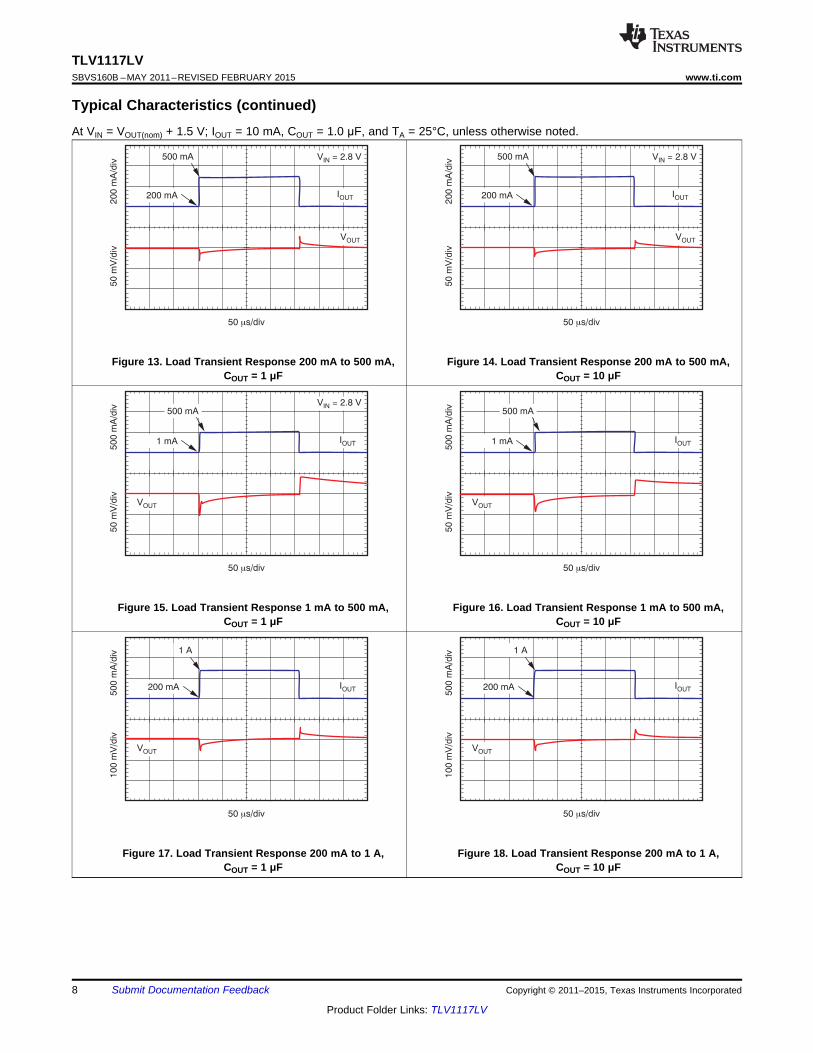
Figure 13. Load Transient Response 200 mA to 500 mA, Figure 14. Load Transient Response 200 mA to 500 mA,COUT = 1 μF COUT = 10 μF
Figure 15. Load Transient Response 1 mA to 500 mA, Figure 16. Load Transient Response 1 mA to 500 mA,COUT = 1 μF COUT = 10 μF
Figure 17. Load Transient Response 200 mA to 1 A, Figure 18. Load Transient Response 200 mA to 1 A,COUT = 1 μF COUT = 10 μF
8 Submit Documentation Feedback Copyright © 2011–2015, Texas Instruments Incorporated
Product Folder Links: TLV1117LV
200 s/divm
10 m
V/d
iv1 V
/div
VIN
VOUT
3.3 V
4.3 V
200 s/divm
10 m
V/d
iv1 V
/div
VIN
VOUT
3.3 V
5.5 V
200 s/divm
5 m
V/d
iv1 V
/div
VIN
VOUT
3.3 V
4.3 V
200 s/divm
5 m
V/d
iv1 V
/div
VIN
VOUT
3.3 V
4.3 V
50 s/divm
100 m
V/d
iv500 m
A/d
iv
IOUT
VOUT
1 mA
1 A
50 s/divm
100 m
V/d
iv500 m
A/d
iv
IOUT
VOUT
1 mA
1 A
TLV1117LVwww.ti.com SBVS160B –MAY 2011–REVISED FEBRUARY 2015
Typical Characteristics (continued)At VIN = VOUT(nom) + 1.5 V; IOUT = 10 mA, COUT = 1.0 μF, and TA = 25°C, unless otherwise noted.
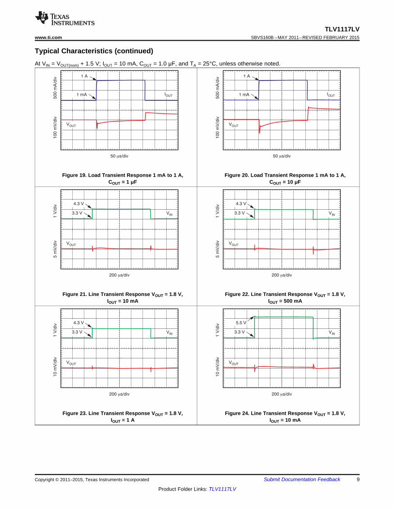
Figure 19. Load Transient Response 1 mA to 1 A, Figure 20. Load Transient Response 1 mA to 1 A,COUT = 1 μF COUT = 10 μF
Figure 21. Line Transient Response VOUT = 1.8 V, Figure 22. Line Transient Response VOUT = 1.8 V,IOUT = 10 mA IOUT = 500 mA
Figure 23. Line Transient Response VOUT = 1.8 V, Figure 24. Line Transient Response VOUT = 1.8 V,IOUT = 1 A IOUT = 10 mA
Copyright © 2011–2015, Texas Instruments Incorporated Submit Documentation Feedback 9
Product Folder Links: TLV1117LV
200 s/divm
10 m
V/d
iv1 V
/div
VIN
VOUT
3.3 V
5.5 V
200 s/divm
10 m
V/d
iv1 V
/div
VIN
VOUT
3.3 V
5.5 V
TLV1117LVSBVS160B –MAY 2011–REVISED FEBRUARY 2015 www.ti.com
Typical Characteristics (continued)At VIN = VOUT(nom) + 1.5 V; IOUT = 10 mA, COUT = 1.0 μF, and TA = 25°C, unless otherwise noted.
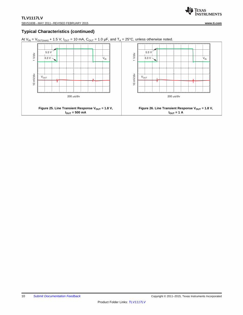
Figure 25. Line Transient Response VOUT = 1.8 V, Figure 26. Line Transient Response VOUT = 1.8 V,IOUT = 500 mA IOUT = 1 A
10 Submit Documentation Feedback Copyright © 2011–2015, Texas Instruments Incorporated
Product Folder Links: TLV1117LV

CurrentLimit
Bandgap
ThermalShutdown
IN OUT
LOGIC
GND
TLV1117LV Series
UVLO
TLV1117LVwww.ti.com SBVS160B –MAY 2011–REVISED FEBRUARY 2015
7 Detailed Description
7.1 OverviewThe TLV1117LV family of devices are a series of low quiescent current, high PSRR LDOs capable of handling upto 1 A of load current. These devices feature an integrated current limit, thermal shutdown, bandgap reference,and UVLO circuit blocks.
7.2 Functional Block Diagram
7.3 Feature Description
7.3.1 Internal Current LimitThe TLV1117LV internal current limit helps to protect the regulator during fault conditions. During current limit,the output sources a fixed amount of current that is largely independent of the output voltage. In such a case, theoutput voltage is not regulated, and can be calculated by the formula: VOUT = ILIMIT × RLOAD. The PMOS passtransistor dissipates (VIN – VOUT) × ILIMIT until thermal shutdown is triggered and the device turns off. As thedevice cools down, it is turned on by the internal thermal shutdown circuit. If the fault condition continues, thedevice cycles between current limit and thermal shutdown. See the Thermal Information section for more details
The PMOS pass element in the TLV1117LV device has a built-in body diode that conducts current when thevoltage at OUT exceeds the voltage at IN. This current is not limited; if extended reverse voltage operation isanticipated, external limiting to 5% of the rated output current is recommended.
7.3.2 Dropout VoltageThe TLV1117LV uses a PMOS pass transistor to achieve low dropout. When (VIN – VOUT) is less than thedropout voltage (VDO), the PMOS pass device is in the linear region of operation and the input-to-outputresistance is the RDS(ON) of the PMOS pass element. VDO scales approximately with output current because thePMOS device behaves as a resistor in dropout.
As with any linear regulator, PSRR and transient response are degraded as (VIN – VOUT) approaches dropout.
Copyright © 2011–2015, Texas Instruments Incorporated Submit Documentation Feedback 11
Product Folder Links: TLV1117LV

TLV1117LVSBVS160B –MAY 2011–REVISED FEBRUARY 2015 www.ti.com
Feature Description (continued)7.3.3 Undervoltage LockoutThe TLV1117LV uses an undervoltage lockout (UVLO) circuit keep the output shut off until internal circuitryoperating properly.
7.4 Device Functional Modes
7.4.1 Normal OperationThe device regulates to the nominal output voltage under the following conditions:
• The input voltage is greater than the nominal output voltage added to the dropout voltage.• The output current is less than the current limit.• The device die temperature is lower than the thermal shutdown temperature.
7.4.2 Dropout OperationIf the input voltage is lower than the nominal output voltage plus the specified dropout voltage, but all otherconditions are met for normal operation, the device operates in dropout mode. In this condition, the outputvoltage is the same the input voltage minus the dropout voltage. The transient performance of the device issignificantly degraded because the pass device is in a triode state and no longer controls the current through theLDO. Line or load transients in dropout may result in large output voltage deviations.
Table 1 shows the conditions that lead to the different modes of operation.
Table 1. Device Functional Mode ComparisonPARAMETER
OPERATING MODEVIN IOUT
Normal mode VIN > VOUT(nom) + VDO IOUT < ICL
Dropout mode VIN < VOUT(nom) + VDO IOUT < ICL
12 Submit Documentation Feedback Copyright © 2011–2015, Texas Instruments Incorporated
Product Folder Links: TLV1117LV

INPUT OUTPUT
GND
DeviceCIN
1 µFCOUT
1 µF
TLV1117LVwww.ti.com SBVS160B –MAY 2011–REVISED FEBRUARY 2015
8 Application and Implementation
NOTEInformation in the following applications sections is not part of the TI componentspecification, and TI does not warrant its accuracy or completeness. TI’s customers areresponsible for determining suitability of components for their purposes. Customers shouldvalidate and test their design implementation to confirm system functionality.
8.1 Application InformationThe TLV1117LV is a low quiescent current linear regulator designed for high current applications. Unlike typicalhigh current linear regulators, the TLV1117LV series consume significantly less quiescent current. These devicesdeliver excellent line and load transient performance. The device is low noise, and exhibits a very good PSRR.As a result, it is ideal for high current applications that require very sensitive power-supply rails.
This family of regulators offers both current limit and thermal protection. The operating junction temperaturerange of the device is –40°C to +125°C.
8.2 Typical ApplicationFigure 27 shows a typical application circuit.
Figure 27. Typical Application Circuit
8.2.1 Design RequirementsFor this design example, use the parameters listed in Table 2 as the input parameters.
Table 2. Design ParametersPARAMETER DESIGN REQUIREMENTInput Voltage 2.5 V to 3.3 V
Output Voltage 1.8 VOutput Current 500 mA
8.2.2 Detailed Design Procedure
8.2.2.1 Input and Output Capacitor RequirementsFor stability, 1.0-μF ceramic capacitors are required at the output. Higher-valued capacitors improve transientperformance. TI recommends the X5R- and X7R-type ceramic capacitors because these capacitors haveminimal variation in value and equivalent series resistance (ESR) over temperature. Unlike traditional linearregulators that need a minimum ESR for stability, the TLV1117LV series are ensured to be stable with no ESR.Therefore, cost-effective ceramic capacitors can be used with these devices. Effective output capacitance thattakes bias, temperature, and aging effects into consideration must be greater than 0.5 μF to ensure stability ofthe device.
Copyright © 2011–2015, Texas Instruments Incorporated Submit Documentation Feedback 13
Product Folder Links: TLV1117LV
V = 2.8 VIN
50 s/divm
50 m
V/d
iv200 m
A/d
iv
IOUT
VOUT
200 mA
500 mA
200 s/divm
5 m
V/d
iv1 V
/div
VIN
VOUT
3.3 V
4.3 V
TLV1117LVSBVS160B –MAY 2011–REVISED FEBRUARY 2015 www.ti.com
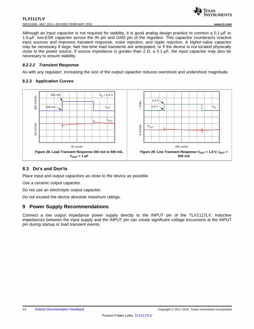
Although an input capacitor is not required for stability, it is good analog design practice to connect a 0.1-μF to1.0-μF, low-ESR capacitor across the IN pin and GND pin of the regulator. This capacitor counteracts reactiveinput sources and improves transient response, noise rejection, and ripple rejection. A higher-value capacitormay be necessary if large, fast rise-time load transients are anticipated, or if the device is not located physicallyclose to the power source. If source impedance is greater than 2 Ω, a 0.1-μF, the input capacitor may also benecessary to ensure stability.
8.2.2.2 Transient ResponseAs with any regulator, increasing the size of the output capacitor reduces overshoot and undershoot magnitude.
8.2.3 Application Curves
Figure 28. Load Transient Response 200 mA to 500 mA, Figure 29. Line Transient Response VOUT = 1.8 V, IOUT =COUT = 1 μF 500 mA
8.3 Do's and Don'tsPlace input and output capacitors as close to the device as possible.
Use a ceramic output capacitor.
Do not use an electrolytic output capacitor.
Do not exceed the device absolute maximum ratings.
9 Power Supply RecommendationsConnect a low output impedance power supply directly to the INPUT pin of the TLV1117LV. Inductiveimpedances between the input supply and the INPUT pin can create significant voltage excursions at the INPUTpin during startup or load transient events.
14 Submit Documentation Feedback Copyright © 2011–2015, Texas Instruments Incorporated
Product Folder Links: TLV1117LV

P = (V V ) I-D IN OUT OUT
Tab
1 2
COUT
3
OUTPUT
GND INPUT
GND
CIN
TLV1117LVwww.ti.com SBVS160B –MAY 2011–REVISED FEBRUARY 2015
10 Layout
10.1 Layout GuidelinesInput and output capacitors should be placed as close to the device pins as possible. To improve characteristicAC performance such as PSRR, output noise, and transient response, TI recommends designing the board withseparate ground planes for VIN and VOUT, with the ground plane connected only at the GND pin of the device. Inaddition, the ground connection for the output capacitor should be connected directly to the GND pin of thedevice. Higher value ESR capacitors may degrade PSRR performance.
10.2 Layout Example
Figure 30. Layout Example
10.3 Thermal ProtectionThermal protection disables the output when the junction temperature rises to approximately 165°C, allowing thedevice to cool. When the junction temperature cools to approximately 145°C, the output circuitry is againenabled. Depending on power dissipation, thermal resistance, and ambient temperature, the thermal protectioncircuit may cycle on and off. This cycling limits the dissipation of the regulator, protecting it from damage as aresult of overheating.
Any tendency to activate the thermal protection circuit indicates excessive power dissipation or an inadequateheatsink. For reliable operation, junction temperature should be limited to 125°C maximum. To estimate themargin of safety in a complete design (including heatsink), increase the ambient temperature until the thermalprotection is triggered; use worst-case loads and signal conditions.
The internal protection circuitry of the TLV1117LV has been designed to protect against overload conditions. Itwas not intended to replace proper heatsinking. Continuously running the TLV1117LV into thermal shutdowndegrades device reliability.
10.4 Power DissipationThe ability to remove heat from the die is different for each package type, presenting different considerations inthe printed circuit board (PCB) layout. The PCB area around the device that is free of other components movesthe heat from the device to the ambient air. Performance data for JEDEC low and high-K boards are given in theThermal Information table. Using heavier copper increases the effectiveness in removing heat from the device.The addition of plated through-holes to heat-dissipating layers also improves heatsink effectiveness.
Power dissipation depends on input voltage and load conditions. Power dissipation (PD) is equal to the product ofthe output current and the voltage drop across the output pass element, as shown in Equation 1:
(1)
Copyright © 2011–2015, Texas Instruments Incorporated Submit Documentation Feedback 15
Product Folder Links: TLV1117LV

TLV1117LVSBVS160B –MAY 2011–REVISED FEBRUARY 2015 www.ti.com
11 Device and Documentation Support
11.1 Device Support
11.1.1 Development Support
11.1.1.1 Evaluation ModuleAn evaluation module (EVM) is available to assist in the initial circuit performance evaluation using theTLV1117LV. The TLV1117LV33EVM-714 evaluation module (and related user's guide) can be requested at theTI website through the product folders or purchased directly from the TI eStore.
11.1.1.2 Spice ModelsComputer simulation of circuit performance using SPICE is often useful when analyzing the performance ofanalog circuits and systems. A SPICE model for the TLV1117LV is available through the product folders underTools & Software.
11.1.2 Device Nomenclature
Table 3. Available Options (1)
PRODUCT VOUT
xx is nominal output voltage (for example 33 = 3.3 V)TLV1117LVxxyyyz yyy is Package Designator
z is Package Quantity
(1) For the most current package and ordering information, see the Package Option Addendum at the end of this document, or visit thedevice product folder at www.ti.com.
11.2 Documentation Support
11.2.1 Related Documentation• TLV1117LV33EVM-714 Evaluation Module User's Guide, SLVU449.
11.3 Related LinksThe table below lists quick access links. Categories include technical documents, support and communityresources, tools and software, and quick access to sample or buy.
Table 4. Related LinksTECHNICAL TOOLS & SUPPORT &PARTS PRODUCT FOLDER SAMPLE & BUY DOCUMENTS SOFTWARE COMMUNITY
TLV1117LV12 Click here Click here Click here Click here Click hereTLV1117LV15 Click here Click here Click here Click here Click hereTLV1117LV18 Click here Click here Click here Click here Click hereTLV1117LV25 Click here Click here Click here Click here Click hereTLV1117LV28 Click here Click here Click here Click here Click hereTLV1117LV30 Click here Click here Click here Click here Click hereTLV1117LV33 Click here Click here Click here Click here Click here
11.4 TrademarksAll trademarks are the property of their respective owners.
11.5 Electrostatic Discharge CautionThese devices have limited built-in ESD protection. The leads should be shorted together or the device placed in conductive foamduring storage or handling to prevent electrostatic damage to the MOS gates.
16 Submit Documentation Feedback Copyright © 2011–2015, Texas Instruments Incorporated
Product Folder Links: TLV1117LV

TLV1117LVwww.ti.com SBVS160B –MAY 2011–REVISED FEBRUARY 2015
11.6 GlossarySLYZ022 — TI Glossary.
This glossary lists and explains terms, acronyms, and definitions.
12 Mechanical, Packaging, and Orderable InformationThe following pages include mechanical, packaging, and orderable information. This information is the mostcurrent data available for the designated devices. This data is subject to change without notice and revision ofthis document. For browser-based versions of this data sheet, refer to the left-hand navigation.
Copyright © 2011–2015, Texas Instruments Incorporated Submit Documentation Feedback 17
Product Folder Links: TLV1117LV

PACKAGE OPTION ADDENDUM
www.ti.com 11-Feb-2015
Addendum-Page 1
PACKAGING INFORMATION
Orderable Device Status(1)
Package Type PackageDrawing
Pins PackageQty
Eco Plan(2)
Lead/Ball Finish(6)
MSL Peak Temp(3)
Op Temp (°C) Device Marking(4/5)
Samples
TLV1117LV12DCYR ACTIVE SOT-223 DCY 4 2500 Green (RoHS& no Sb/Br)
CU SN Level-1-260C-UNLIM -40 to 125 SI
TLV1117LV12DCYT ACTIVE SOT-223 DCY 4 250 Green (RoHS& no Sb/Br)
CU SN Level-1-260C-UNLIM -40 to 125 SI
TLV1117LV15DCYR ACTIVE SOT-223 DCY 4 2500 Green (RoHS& no Sb/Br)
CU SN Level-1-260C-UNLIM -40 to 125 VR
TLV1117LV15DCYT ACTIVE SOT-223 DCY 4 250 Green (RoHS& no Sb/Br)
CU SN Level-1-260C-UNLIM -40 to 125 VR
TLV1117LV18DCYR ACTIVE SOT-223 DCY 4 2500 Green (RoHS& no Sb/Br)
CU SN Level-1-260C-UNLIM -40 to 125 SH
TLV1117LV18DCYT ACTIVE SOT-223 DCY 4 250 Green (RoHS& no Sb/Br)
CU SN Level-1-260C-UNLIM -40 to 125 SH
TLV1117LV25DCYR ACTIVE SOT-223 DCY 4 2500 Green (RoHS& no Sb/Br)
CU SN Level-1-260C-UNLIM -40 to 125 VS
TLV1117LV25DCYT ACTIVE SOT-223 DCY 4 250 Green (RoHS& no Sb/Br)
CU SN Level-1-260C-UNLIM -40 to 125 VS
TLV1117LV28DCYR ACTIVE SOT-223 DCY 4 2500 Green (RoHS& no Sb/Br)
CU SN Level-1-260C-UNLIM -40 to 125 VT
TLV1117LV28DCYT ACTIVE SOT-223 DCY 4 250 Green (RoHS& no Sb/Br)
CU SN Level-1-260C-UNLIM -40 to 125 VT
TLV1117LV30DCYR ACTIVE SOT-223 DCY 4 2500 Green (RoHS& no Sb/Br)
CU SN Level-1-260C-UNLIM -40 to 125 VU
TLV1117LV30DCYT ACTIVE SOT-223 DCY 4 250 Green (RoHS& no Sb/Br)
CU SN Level-1-260C-UNLIM -40 to 125 VU
TLV1117LV33DCYR ACTIVE SOT-223 DCY 4 2500 Green (RoHS& no Sb/Br)
CU SN Level-1-260C-UNLIM -40 to 125 TJ
TLV1117LV33DCYT ACTIVE SOT-223 DCY 4 250 Green (RoHS& no Sb/Br)
CU SN Level-1-260C-UNLIM -40 to 125 TJ
(1) The marketing status values are defined as follows:ACTIVE: Product device recommended for new designs.LIFEBUY: TI has announced that the device will be discontinued, and a lifetime-buy period is in effect.NRND: Not recommended for new designs. Device is in production to support existing customers, but TI does not recommend using this part in a new design.PREVIEW: Device has been announced but is not in production. Samples may or may not be available.OBSOLETE: TI has discontinued the production of the device.

PACKAGE OPTION ADDENDUM
www.ti.com 11-Feb-2015
Addendum-Page 2
(2) Eco Plan - The planned eco-friendly classification: Pb-Free (RoHS), Pb-Free (RoHS Exempt), or Green (RoHS & no Sb/Br) - please check http://www.ti.com/productcontent for the latest availabilityinformation and additional product content details.TBD: The Pb-Free/Green conversion plan has not been defined.Pb-Free (RoHS): TI's terms "Lead-Free" or "Pb-Free" mean semiconductor products that are compatible with the current RoHS requirements for all 6 substances, including the requirement thatlead not exceed 0.1% by weight in homogeneous materials. Where designed to be soldered at high temperatures, TI Pb-Free products are suitable for use in specified lead-free processes.Pb-Free (RoHS Exempt): This component has a RoHS exemption for either 1) lead-based flip-chip solder bumps used between the die and package, or 2) lead-based die adhesive used betweenthe die and leadframe. The component is otherwise considered Pb-Free (RoHS compatible) as defined above.Green (RoHS & no Sb/Br): TI defines "Green" to mean Pb-Free (RoHS compatible), and free of Bromine (Br) and Antimony (Sb) based flame retardants (Br or Sb do not exceed 0.1% by weightin homogeneous material)
(3) MSL, Peak Temp. - The Moisture Sensitivity Level rating according to the JEDEC industry standard classifications, and peak solder temperature.
(4) There may be additional marking, which relates to the logo, the lot trace code information, or the environmental category on the device.
(5) Multiple Device Markings will be inside parentheses. Only one Device Marking contained in parentheses and separated by a "~" will appear on a device. If a line is indented then it is a continuationof the previous line and the two combined represent the entire Device Marking for that device.
(6) Lead/Ball Finish - Orderable Devices may have multiple material finish options. Finish options are separated by a vertical ruled line. Lead/Ball Finish values may wrap to two lines if the finishvalue exceeds the maximum column width.
Important Information and Disclaimer:The information provided on this page represents TI's knowledge and belief as of the date that it is provided. TI bases its knowledge and belief on informationprovided by third parties, and makes no representation or warranty as to the accuracy of such information. Efforts are underway to better integrate information from third parties. TI has taken andcontinues to take reasonable steps to provide representative and accurate information but may not have conducted destructive testing or chemical analysis on incoming materials and chemicals.TI and TI suppliers consider certain information to be proprietary, and thus CAS numbers and other limited information may not be available for release.
In no event shall TI's liability arising out of such information exceed the total purchase price of the TI part(s) at issue in this document sold by TI to Customer on an annual basis.
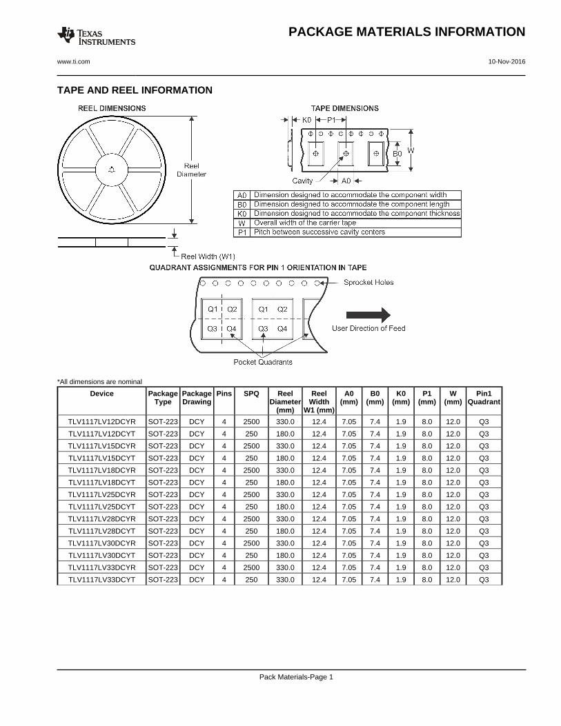
TAPE AND REEL INFORMATION
*All dimensions are nominal
Device PackageType
PackageDrawing
Pins SPQ ReelDiameter
(mm)
ReelWidth
W1 (mm)
A0(mm)
B0(mm)
K0(mm)
P1(mm)
W(mm)
Pin1Quadrant
TLV1117LV12DCYR SOT-223 DCY 4 2500 330.0 12.4 7.05 7.4 1.9 8.0 12.0 Q3
TLV1117LV12DCYT SOT-223 DCY 4 250 180.0 12.4 7.05 7.4 1.9 8.0 12.0 Q3
TLV1117LV15DCYR SOT-223 DCY 4 2500 330.0 12.4 7.05 7.4 1.9 8.0 12.0 Q3
TLV1117LV15DCYT SOT-223 DCY 4 250 180.0 12.4 7.05 7.4 1.9 8.0 12.0 Q3
TLV1117LV18DCYR SOT-223 DCY 4 2500 330.0 12.4 7.05 7.4 1.9 8.0 12.0 Q3
TLV1117LV18DCYT SOT-223 DCY 4 250 180.0 12.4 7.05 7.4 1.9 8.0 12.0 Q3
TLV1117LV25DCYR SOT-223 DCY 4 2500 330.0 12.4 7.05 7.4 1.9 8.0 12.0 Q3
TLV1117LV25DCYT SOT-223 DCY 4 250 180.0 12.4 7.05 7.4 1.9 8.0 12.0 Q3
TLV1117LV28DCYR SOT-223 DCY 4 2500 330.0 12.4 7.05 7.4 1.9 8.0 12.0 Q3
TLV1117LV28DCYT SOT-223 DCY 4 250 180.0 12.4 7.05 7.4 1.9 8.0 12.0 Q3
TLV1117LV30DCYR SOT-223 DCY 4 2500 330.0 12.4 7.05 7.4 1.9 8.0 12.0 Q3
TLV1117LV30DCYT SOT-223 DCY 4 250 180.0 12.4 7.05 7.4 1.9 8.0 12.0 Q3
TLV1117LV33DCYR SOT-223 DCY 4 2500 330.0 12.4 7.05 7.4 1.9 8.0 12.0 Q3
TLV1117LV33DCYT SOT-223 DCY 4 250 330.0 12.4 7.05 7.4 1.9 8.0 12.0 Q3
PACKAGE MATERIALS INFORMATION
www.ti.com 10-Nov-2016
Pack Materials-Page 1

*All dimensions are nominal
Device Package Type Package Drawing Pins SPQ Length (mm) Width (mm) Height (mm)
TLV1117LV12DCYR SOT-223 DCY 4 2500 340.0 340.0 38.0
TLV1117LV12DCYT SOT-223 DCY 4 250 340.0 340.0 38.0
TLV1117LV15DCYR SOT-223 DCY 4 2500 340.0 340.0 38.0
TLV1117LV15DCYT SOT-223 DCY 4 250 340.0 340.0 38.0
TLV1117LV18DCYR SOT-223 DCY 4 2500 340.0 340.0 38.0
TLV1117LV18DCYT SOT-223 DCY 4 250 340.0 340.0 38.0
TLV1117LV25DCYR SOT-223 DCY 4 2500 340.0 340.0 38.0
TLV1117LV25DCYT SOT-223 DCY 4 250 340.0 340.0 38.0
TLV1117LV28DCYR SOT-223 DCY 4 2500 340.0 340.0 38.0
TLV1117LV28DCYT SOT-223 DCY 4 250 340.0 340.0 38.0
TLV1117LV30DCYR SOT-223 DCY 4 2500 340.0 340.0 38.0
TLV1117LV30DCYT SOT-223 DCY 4 250 340.0 340.0 38.0
TLV1117LV33DCYR SOT-223 DCY 4 2500 340.0 340.0 38.0
TLV1117LV33DCYT SOT-223 DCY 4 250 340.0 340.0 38.0
PACKAGE MATERIALS INFORMATION
www.ti.com 10-Nov-2016
Pack Materials-Page 2
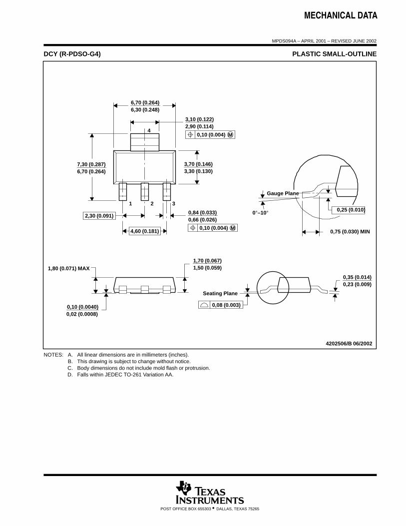
MECHANICAL DATA
MPDS094A – APRIL 2001 – REVISED JUNE 2002
POST OFFICE BOX 655303 • DALLAS, TEXAS 75265
DCY (R-PDSO-G4) PLASTIC SMALL-OUTLINE
4202506/B 06/2002
6,30 (0.248)6,70 (0.264)
2,90 (0.114)3,10 (0.122)
6,70 (0.264)7,30 (0.287) 3,70 (0.146)
3,30 (0.130)
0,02 (0.0008)0,10 (0.0040)
1,50 (0.059)1,70 (0.067)
0,23 (0.009)0,35 (0.014)
1 2 3
4
0,66 (0.026)0,84 (0.033)
1,80 (0.071) MAX
Seating Plane
0°–10°
Gauge Plane
0,75 (0.030) MIN
0,25 (0.010)
0,08 (0.003)
0,10 (0.004) M
2,30 (0.091)
4,60 (0.181) M0,10 (0.004)
NOTES: A. All linear dimensions are in millimeters (inches).B. This drawing is subject to change without notice.C. Body dimensions do not include mold flash or protrusion.D. Falls within JEDEC TO-261 Variation AA.


IMPORTANT NOTICE
Texas Instruments Incorporated and its subsidiaries (TI) reserve the right to make corrections, enhancements, improvements and otherchanges to its semiconductor products and services per JESD46, latest issue, and to discontinue any product or service per JESD48, latestissue. Buyers should obtain the latest relevant information before placing orders and should verify that such information is current andcomplete. All semiconductor products (also referred to herein as “components”) are sold subject to TI’s terms and conditions of salesupplied at the time of order acknowledgment.TI warrants performance of its components to the specifications applicable at the time of sale, in accordance with the warranty in TI’s termsand conditions of sale of semiconductor products. Testing and other quality control techniques are used to the extent TI deems necessaryto support this warranty. Except where mandated by applicable law, testing of all parameters of each component is not necessarilyperformed.TI assumes no liability for applications assistance or the design of Buyers’ products. Buyers are responsible for their products andapplications using TI components. To minimize the risks associated with Buyers’ products and applications, Buyers should provideadequate design and operating safeguards.TI does not warrant or represent that any license, either express or implied, is granted under any patent right, copyright, mask work right, orother intellectual property right relating to any combination, machine, or process in which TI components or services are used. Informationpublished by TI regarding third-party products or services does not constitute a license to use such products or services or a warranty orendorsement thereof. Use of such information may require a license from a third party under the patents or other intellectual property of thethird party, or a license from TI under the patents or other intellectual property of TI.Reproduction of significant portions of TI information in TI data books or data sheets is permissible only if reproduction is without alterationand is accompanied by all associated warranties, conditions, limitations, and notices. TI is not responsible or liable for such altereddocumentation. Information of third parties may be subject to additional restrictions.Resale of TI components or services with statements different from or beyond the parameters stated by TI for that component or servicevoids all express and any implied warranties for the associated TI component or service and is an unfair and deceptive business practice.TI is not responsible or liable for any such statements.Buyer acknowledges and agrees that it is solely responsible for compliance with all legal, regulatory and safety-related requirementsconcerning its products, and any use of TI components in its applications, notwithstanding any applications-related information or supportthat may be provided by TI. Buyer represents and agrees that it has all the necessary expertise to create and implement safeguards whichanticipate dangerous consequences of failures, monitor failures and their consequences, lessen the likelihood of failures that might causeharm and take appropriate remedial actions. Buyer will fully indemnify TI and its representatives against any damages arising out of the useof any TI components in safety-critical applications.In some cases, TI components may be promoted specifically to facilitate safety-related applications. With such components, TI’s goal is tohelp enable customers to design and create their own end-product solutions that meet applicable functional safety standards andrequirements. Nonetheless, such components are subject to these terms.No TI components are authorized for use in FDA Class III (or similar life-critical medical equipment) unless authorized officers of the partieshave executed a special agreement specifically governing such use.Only those TI components which TI has specifically designated as military grade or “enhanced plastic” are designed and intended for use inmilitary/aerospace applications or environments. Buyer acknowledges and agrees that any military or aerospace use of TI componentswhich have not been so designated is solely at the Buyer's risk, and that Buyer is solely responsible for compliance with all legal andregulatory requirements in connection with such use.TI has specifically designated certain components as meeting ISO/TS16949 requirements, mainly for automotive use. In any case of use ofnon-designated products, TI will not be responsible for any failure to meet ISO/TS16949.
Products ApplicationsAudio www.ti.com/audio Automotive and Transportation www.ti.com/automotiveAmplifiers amplifier.ti.com Communications and Telecom www.ti.com/communicationsData Converters dataconverter.ti.com Computers and Peripherals www.ti.com/computersDLP® Products www.dlp.com Consumer Electronics www.ti.com/consumer-appsDSP dsp.ti.com Energy and Lighting www.ti.com/energyClocks and Timers www.ti.com/clocks Industrial www.ti.com/industrialInterface interface.ti.com Medical www.ti.com/medicalLogic logic.ti.com Security www.ti.com/securityPower Mgmt power.ti.com Space, Avionics and Defense www.ti.com/space-avionics-defenseMicrocontrollers microcontroller.ti.com Video and Imaging www.ti.com/videoRFID www.ti-rfid.comOMAP Applications Processors www.ti.com/omap TI E2E Community e2e.ti.comWireless Connectivity www.ti.com/wirelessconnectivity
Mailing Address: Texas Instruments, Post Office Box 655303, Dallas, Texas 75265Copyright © 2016, Texas Instruments Incorporated


