Thermodynamics in Chip Processing II Terry A. Ring.
31
Thermodynamics in Chip Processing II Terry A. Ring
-
Upload
ginger-kelley -
Category
Documents
-
view
218 -
download
2
Transcript of Thermodynamics in Chip Processing II Terry A. Ring.

Thermodynamics in Chip Processing II
Terry A. Ring
CVD

Materials Deposited
• Dielectrics– SiO2, BSG
• Metals– W, Cu, Al
• Semiconductors– Poly silicon (doped)
• Barrier Layers– Nitrides (TaN, TiN), Silicides (WSi2, TaSi2, CoSi,
MoSi2)
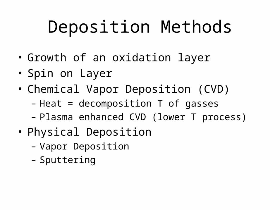
Deposition Methods
• Growth of an oxidation layer• Spin on Layer• Chemical Vapor Deposition (CVD)
– Heat = decomposition T of gasses– Plasma enhanced CVD (lower T process)
• Physical Deposition– Vapor Deposition– Sputtering

Critical Issues
• Adherence of the layer• Chemical Compatibility
– Electro Migration– Inter diffusion during subsequent processing
• Strong function of Processing
• Even Deposition at all wafer locations

CVD of Si3N4 - Implantation mask
• 3 SiH2Cl2 + 4 NH3Si3N4 + 6 HCl + 6 H2
– 780C, vacuum
– Carrier gas with NH3 / SiH2Cl2 >>1
• Stack of wafer into furnace– Higher temperature at exit to compensate for gas
conversion losses
• Add gases• Stop after layer is thick enough
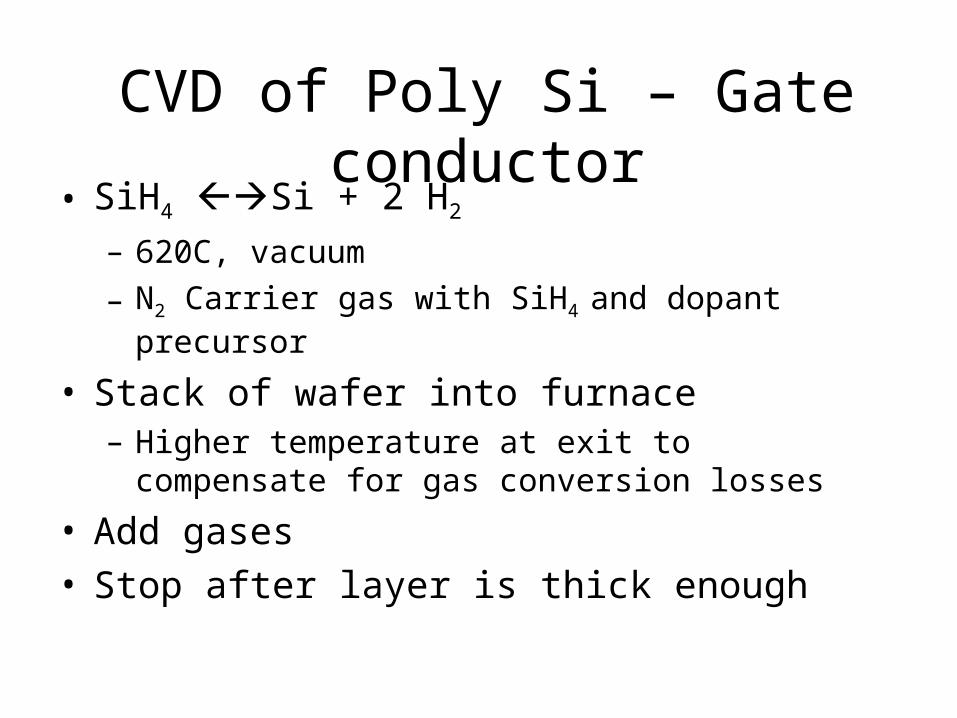
CVD of Poly Si – Gate conductor• SiH4 Si + 2 H2
– 620C, vacuum
– N2 Carrier gas with SiH4 and dopant precursor
• Stack of wafer into furnace– Higher temperature at exit to compensate for gas
conversion losses
• Add gases• Stop after layer is thick enough
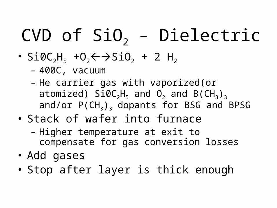
CVD of SiO2 – Dielectric• Si0C2H5 +O2SiO2 + 2 H2
– 400C, vacuum– He carrier gas with vaporized(or atomized) Si0C2H5
and O2 and B(CH3)3 and/or P(CH3)3 dopants for BSG and BPSG
• Stack of wafer into furnace– Higher temperature at exit to compensate for gas
conversion losses
• Add gases• Stop after layer is thick enough

CVD of W – Metal plugs
• 3H2+WF6 W + 6HF– T>800C, vacuum– He carrier gas with WF6
– Side Reactions at lower temperatures• Oxide etching reactions• 2H2+2WF6+3SiO2 3SiF4 + 2WO2 + 2H2O• SiO2 + 4HF 2H2O +SiF4
• Stack of wafer into furnace– Higher temperature at exit to compensate for gas conversion
losses
• Add gases• Stop after layer is thick enough
Chemical Equilibrium
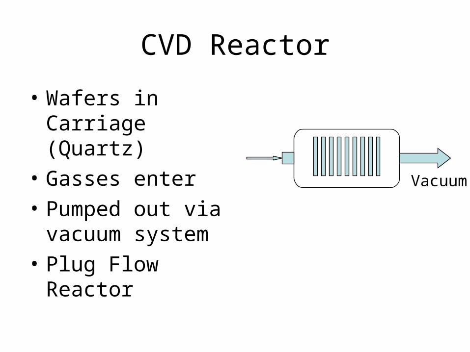
CVD Reactor
• Wafers in Carriage (Quartz)
• Gasses enter
• Pumped out via vacuum system
• Plug Flow Reactor
Vacuum

CVD Reactor
• Macroscopic Analysis– Plug flow reactor
• Microscopic Analysis– Surface Reaction
• Film Growth Rate
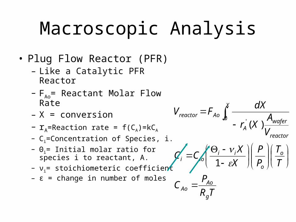
Macroscopic Analysis
• Plug Flow Reactor (PFR)– Like a Catalytic PFR Reactor– FAo= Reactant Molar Flow
Rate– X = conversion– rA=Reaction rate = f(CA)=kCA
– Ci=Concentration of Species, i.– Θi= Initial molar ratio for species i to
reactant, A.– νi= stoichiometeric coefficient– ε = change in number of moles
TR
PC
T
T
P
P
X
XCC
V
AXr
dXFV
g
AoAo
o
o
iiioi
X
reactor
waferA
Aoreactor
1
)(0
'

Combined Effects
Contours = Concentration

Reactor Length Effects
SiH2Cl2(g) + 2 N2O(g) SiO2(s)+ 2 N2(g)+2 HCl(g)
nwafer VReactorPerWafer a
FAo0
X
X1
r'A X( )
d n X( )FAo
VReactorPerWafer a 0
X
X1
r'A X( )
d
rate X( )
r'A X( )4
Dwafer2
SiO2
MwSiO2Awafer
0 50 100 1500
2000
4000
6000
Wafer Number
Th
ick
ness
(nm
)
rate X'( ) 10 minnm
n X'( )0 0.5 10
200
400
600
Conversion
Dep
osi
tio
n R
ate
, W
afe
r N
um
ber
rate X( )
nm
min
n X( )
X
How to solve? Higher T at exit!

Deposition Rate over the Radius
r
wAsA
A
pABe
wA
Ae
RrCC
rfiniteC
ConditionsBoundary
DD
V
Ar
dr
CdrD
dr
d
r
,
0,
1 "
CAs
Thiele Modulus Φ1=(2kRw/DABx)1/2

Radial Effects
This is bad!!!
Pseudo First Order Results
CA 1
sinh 1 sinh 1
00.510.97
0.98
0.99
1
r/R.wafer
Con
cent
rati
on
CA
00.51
4900
4950
5000
5050
r/R.wafer
Thi
ckne
ss(n
m)
rate 1 CA 10 min
nm
x 0.5

Combined Length and Radial Effects
00.512400
2600
2800
3000
3200
3400
3600
r/R.wafer
Th
ick
ness
Rate 10 10 minnm
Rate 20 10 minnm
Wafer 20
Wafer 10
CVD Reactor
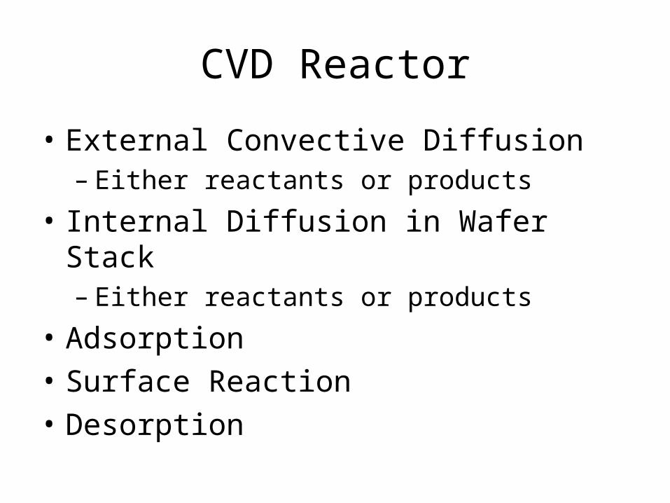
• External Convective Diffusion– Either reactants or products
• Internal Diffusion in Wafer Stack– Either reactants or products
• Adsorption
• Surface Reaction
• Desorption

Microscopic Analysis -Reaction Steps
• Adsorption – A(g)+SA*S– rAD=kAD (PACv-CA*S/KAD)
• Surface Reaction-1 – A*S+SS*S + C*S
– rS=kS(CvCA*S - Cv CC*S/KS)
• Surface Reaction-2– A*S+B*SS*S+C*S+P(g)– rS=kS(CA*SCB*S - Cv CC*SPP/KS)
• Desorption: C*S<----> C(g) +S– rD=kD(CC*S-PCCv/KD)
• Any can be rate determining! Others in Equilib.• Write in terms of gas pressures, total site conc.

CMP
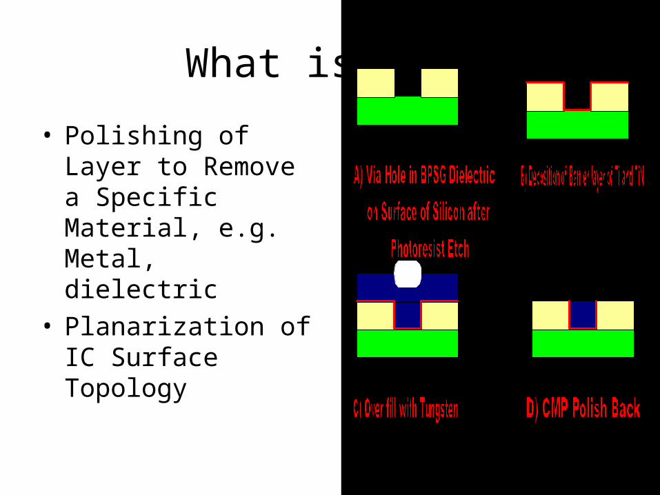
What is CMP?
• Polishing of Layer to Remove a Specific Material, e.g. Metal, dielectric
• Planarization of IC Surface Topology
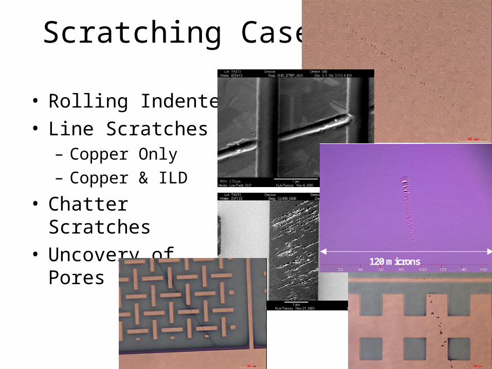
Scratching Cases
• Rolling Indenter• Line Scratches
– Copper Only– Copper & ILD
• Chatter Scratches• Uncovery of Pores
120 microns

CMP Tooling
• Rotating Multi-head Wafer Carriage
• Rotating Pad• Wafer Rests on Film of
Slurry • Velocity= -
(WtRcc)–[Rh(Wh –Wt)] • when Wh=Wt
Velocity = const.
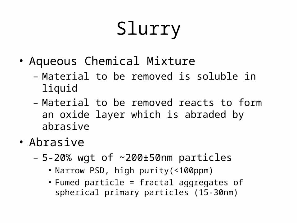
Slurry
• Aqueous Chemical Mixture– Material to be removed is soluble in liquid– Material to be removed reacts to form an oxide layer
which is abraded by abrasive
• Abrasive– 5-20% wgt of ~200±50nm particles
• Narrow PSD, high purity(<100ppm)• Fumed particle = fractal aggregates of spherical primary
particles (15-30nm)
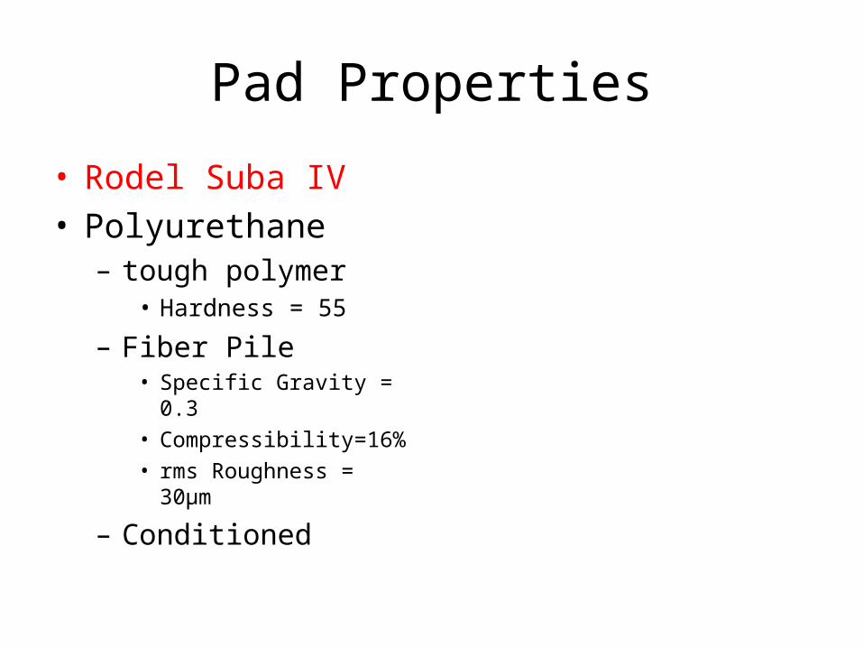
Pad Properties
• Rodel Suba IV• Polyurethane
– tough polymer• Hardness = 55
– Fiber Pile• Specific Gravity = 0.3
• Compressibility=16%
• rms Roughness = 30μm
– Conditioned
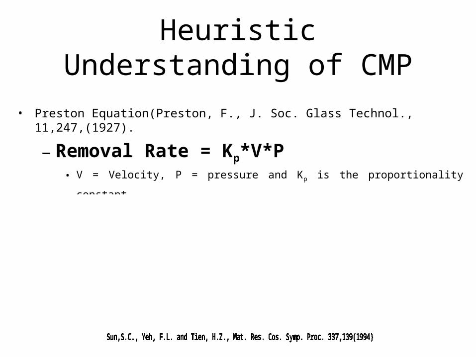
Heuristic Understanding of CMP
• Preston Equation(Preston, F., J. Soc. Glass Technol., 11,247,(1927).
– Removal Rate = Kp*V*P• V = Velocity, P = pressure and Kp is the proportionality constant.

CMP Pad Modeling• Pad Mechanical Model - Planar Pad
• Warnock,J.,J. Electrochemical Soc.138(8)2398-402(1991).
• Does not account for Pad Microstructure

CMP Modeling
• Numerical Model of Flow under Wafer– 3D-Runnels, S.R. and Eyman, L.M., J. Electrochemical Soc.
141,1698(1994).
– 2-D-Sundararajan, S., Thakurta, D.G., Schwendeman, D.W., Muraraka, S.P. and Gill, W.N., J. Electrochemical Soc. 146(2),761-766(1999).
PadU
Pappliedy
x
h(x)
Wafer
Slurry
D
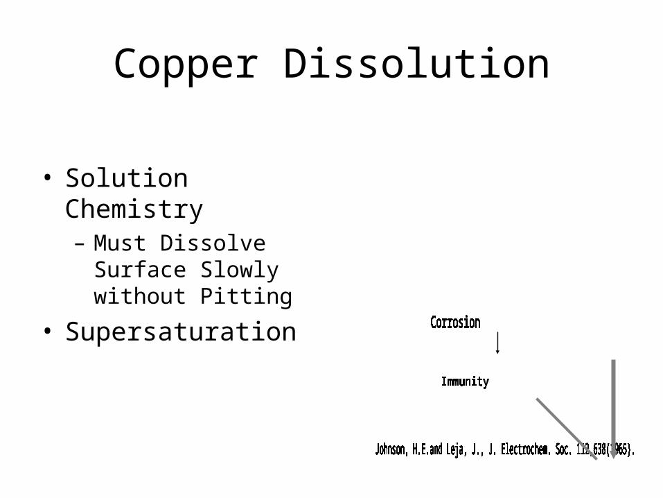
Copper Dissolution
• Solution Chemistry– Must Dissolve Surface
Slowly without Pitting
• Supersaturation
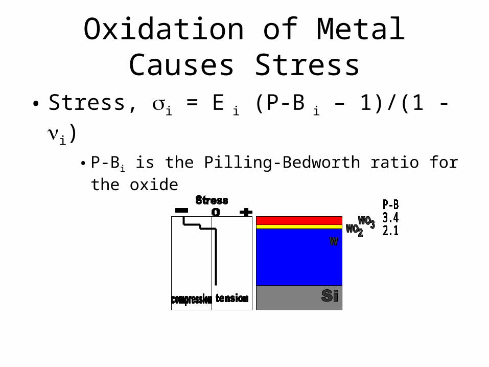
Oxidation of Metal Causes Stress
• Stress, i = E i (P-B i – 1)/(1 - i)• P-Bi is the Pilling-Bedworth ratio for the oxide