![Geoethics - Earth-prints...Geoethics : ethical challenges and case studies in earth sciences / [edited by] Max Wyss, Silvia Peppoloni. pages cm Includes bibliographical references](https://static.fdocuments.us/doc/165x107/5fd774c11f0b87532354f28f/geoethics-earth-prints-geoethics-ethical-challenges-and-case-studies-in.jpg)
The New AIS Design Report - Home | Earth-prints
60
1 THE NEW INGV DIGITAL IONOSONDE DESIGN REPORT J. Baskaradas Arokiasamy, C.Bianchi, U. Sciacca, G. Tutone, E. Zuccheretti Abstract The ionosonde is a system which exploits the radar technique: it applies electromagnetic waves with variable frequency in the HF band to measure the ionospheric layers electron density, height and other parameters. This paper is a technical report on the new digital ionosonde (AIS-INGV), which was designed both for research purposes and for the routine service of the HF radiowave propagation forecast. It has been developed almost completely within the Laboratorio di Geofisica Ambientale (LGA) at the Istituto Nazionale di Geofisica e Vulcanologia (INGV). It exploits advanced techniques for the signal analysis, recent technological devices and PC resources. The report is divided into two parts; the first is a general description of the design development, the second is a more detailed description of the blocks and circuits actually built and tested, directed to a specialist reader. 1. INTRODUCTION 1.1 The needs of sounding the ionosphere Traditionally it is called ionosphere those part of the atmosphere that shows a conspicuous ionisation of the medium, i.e. there is a concentration of electrons and ions much greater than outside of it, this ionisation being due mainly to the X and UV radiation coming from the Sun. Even though the most relevant interest in the study of the ionosphere lies in the applications on the radio propagation, other topics are investigated, such as the relationships with the earth magnetic field and the climatology. Historically the term “ionosphere” was adopted to highlight the fact that the ionisation was sufficient to influence the propagation of radio waves in such a way to make possible long distance links on the Earth. Almost every electromagnetic wave is influenced by the ionosphere, but those which are deviated in such a way to make possible the above mentioned links are only those with a frequency between 30 kHz and 25÷30 MHz, i.e. using the international names for the radio bands, the LF, MF and HF bands are involved. Anyway, also the radio waves at higher frequencies can be attenuated and deviated passing through the ionosphere. So the ionosphere has importance also in such services like the satellite links or the GPS. The ionisation is not constant at different heights, this gives rise to layers with different electron density N, as it is possible to see examining a density profile like the one in fig. 1.1. The ionised layers are identified by a letter: D, E, F (F1 and F2) and stay approximately between 50 and 1000 km, so they spread over the mesosphere and the thermosphere and correspond to the peaks of N (not always so evident). Obviously their position and strength changes accordingly to the solar radiation, showing cycles along a single day, the seasons, and the solar 11-years cycle. Also the position on the earth affects the ionisation; mostly the latitude, but also the magnetic field can influence it. In order to accomplish a ionospheric radio link some parameters have to be determined, as: the frequency of the carrier, the transmitted power, the type of modulation, the angle of radiation, etc. The work can be carry out knowing the profile of ionisation, or at least some parameters related to it. Actually, the profile is not known and it has to be inferred by means of a proper sounding of the medium carried out by means of a dedicated radar called ionosonde. A ionosonde traditionally sends a radiowave towards the ionosphere, almost always in vertical direction, and, examining the delay of the received echo, it infers the height which the reflection occurred at. Being the reflection a not perfect one, i.e. it does not occur over a perfect mirror, the calculated height is only a “virtual” one and it is insufficient to infer the real height of the reflecting layer. It is only by means of a multiple sounding at different frequencies that it is possible to “invert” the data and get the ionisation profile.
Transcript of The New AIS Design Report - Home | Earth-prints

1
THE NEW INGV DIGITAL IONOSONDE
DESIGN REPORT
J. Baskaradas Arokiasamy, C.Bianchi, U. Sciacca, G. Tutone, E. Zuccheretti
Abstract The ionosonde is a system which exploits the radar technique: it applies electromagnetic waves with
variable frequency in the HF band to measure the ionospheric layers electron density, height and other parameters. This paper is a technical report on the new digital ionosonde (AIS-INGV), which was designed both for research purposes and for the routine service of the HF radiowave propagation forecast. It has been developed almost completely within the Laboratorio di Geofisica Ambientale (LGA) at the Istituto Nazionale di Geofisica e Vulcanologia (INGV). It exploits advanced techniques for the signal analysis, recent technological devices and PC resources. The report is divided into two parts; the first is a general description of the design development, the second is a more detailed description of the blocks and circuits actually built and tested, directed to a specialist reader.
1. INTRODUCTION 1.1 The needs of sounding the ionosphere
Traditionally it is called ionosphere those part of the atmosphere that shows a conspicuous ionisation
of the medium, i.e. there is a concentration of electrons and ions much greater than outside of it, this ionisation being due mainly to the X and UV radiation coming from the Sun. Even though the most relevant interest in the study of the ionosphere lies in the applications on the radio propagation, other topics are investigated, such as the relationships with the earth magnetic field and the climatology.
Historically the term “ionosphere” was adopted to highlight the fact that the ionisation was sufficient to influence the propagation of radio waves in such a way to make possible long distance links on the Earth. Almost every electromagnetic wave is influenced by the ionosphere, but those which are deviated in such a way to make possible the above mentioned links are only those with a frequency between 30 kHz and 25÷30 MHz, i.e. using the international names for the radio bands, the LF, MF and HF bands are involved. Anyway, also the radio waves at higher frequencies can be attenuated and deviated passing through the ionosphere. So the ionosphere has importance also in such services like the satellite links or the GPS.
The ionisation is not constant at different heights, this gives rise to layers with different electron density N, as it is possible to see examining a density profile like the one in fig. 1.1. The ionised layers are identified by a letter: D, E, F (F1 and F2) and stay approximately between 50 and 1000 km, so they spread over the mesosphere and the thermosphere and correspond to the peaks of N (not always so evident). Obviously their position and strength changes accordingly to the solar radiation, showing cycles along a single day, the seasons, and the solar 11-years cycle. Also the position on the earth affects the ionisation; mostly the latitude, but also the magnetic field can influence it.
In order to accomplish a ionospheric radio link some parameters have to be determined, as: the frequency of the carrier, the transmitted power, the type of modulation, the angle of radiation, etc. The work can be carry out knowing the profile of ionisation, or at least some parameters related to it. Actually, the profile is not known and it has to be inferred by means of a proper sounding of the medium carried out by means of a dedicated radar called ionosonde.
A ionosonde traditionally sends a radiowave towards the ionosphere, almost always in vertical direction, and, examining the delay of the received echo, it infers the height which the reflection occurred at. Being the reflection a not perfect one, i.e. it does not occur over a perfect mirror, the calculated height is only a “virtual” one and it is insufficient to infer the real height of the reflecting layer. It is only by means of a multiple sounding at different frequencies that it is possible to “invert” the data and get the ionisation profile.

2
Fig.1.1 – A typical electron density profile
Anyway, also the “rough” data, containing only the virtual heights versus frequency, may be sufficient
to get the relevant parameters to be used to design a link. This kind of graph, with the virtual heights, is called “ionogram”; an example is shown in fig.1.2, where the just mentioned relevant points have been highlighted. The not horizontal shape of the layers is due to the not constant speed of propagation in the medium; it appears clear the not correspondence between the displayed height (virtual) and the actual one: at some frequencies, called “critical” (f0X, X= E, F1, F2), the echo appears to arrive even from a very far distance, much greater than that typical at frequencies just lesser than them. The second profile (in green) is due to the so called “extraordinary” ray, the result of a birefringence phenomenon into the medium, due to the earth magnetic field.
Fig.1.2 – Ionogram example
The ionogram is the “traditional” output of a ionosonde system; the recent developments have brought
to additional outputs, for instance the drift velocity of the layers or even directly the electron density profile (see also the end of the next paragraph). More information on the propagation in the ionosphere is available in the large literature on this subject (for example see [Bianchi 1990]).
3
1.2 A brief history of ionospheric technology The modern ionosondes sink their roots in the past ionospheric sounding experience. The ionosonde
was the forerunner of the modern pulsed radar, even though continuous wave (CW) interference technique was used at first to probe the ionosphere. A radar technique based on CW interference followed quickly the first radio. In fact, an electromagnetic system able to detect and locate reflecting surfaces was developed since the beginning of the past century (1903) by Christian Hülsmeyer who patented his system in several countries [Skolnik 1980]. The stage of the technology at that epoch was insufficient to give practical results. The range, a little more than one km, did not encourage its application, and for about two decades scientists lost interest in this field. Guglielmo Marconi experienced himself the reflection of radio waves by conducting layers (ionosphere) since his first transcontinental radio connection and, later, using short wave reflection from moving large objects like ships. He put all its authority on this subject, and in a memorable speech [Marconi 1922] he said:
[…] It seems to me that it should be possible to design an apparatus by means of which a ship could radiate rays in any desired direction, which rays, if coming across a metallic object, such as another streamer or ship, would be reflected back to a receiver screened from the local transmitter on the sending ship, and thereby, immediately reveal the presence and bearing of other ship in a fog or thick weather.
From these sentences, it appears clear that CW interference should be employed and the pulsed techniques was not considered yet. In fact, by means of this radio technique, based on the phase difference between the sky and ground wave, Appletton and Barnett were able to infer the height of the ionospheric layers [Appletton and Barnett 1925]. The first pulsed radar was developed by G. Beit and M.A. Tuve in USA and it was also the first experiment on which the height of a conducting layer in upper atmosphere was measured [Beit and Tuve 1926]. The line had been drawn, and after that the scientists worked frantically while the radio technology had been increasing tremendously, especially for communication purposes. The new pulsed radar (now called ionosonde) became the preferred one because, compared with the pulsed technique that directly could yield the exact distance (range), CW interference technique (in various forms) was not competitive.
The years during and after the World War II were the most significant ones for the development of modern radars. The progresses in such a field were observed day by day: starting from the employment of waves shorter and shorter till to the using of the cavity-magnetron, from new sophisticated antennas to new switching systems. The introduction of some analysis of the received signal to extract useful information on the nature of the targets (MTI and ADT radar) was another decisive step. In the late sixties scientists tried to solve another problem: the transmitted power. For years, in order to increase the S/N ratio, brutal force was used employing kWs of transmitted power in all radars, ionosondes included.
At the beginning of 1970s a new generation of ionosondes, with some kind of internal processor or computer-interfaced, capable of measuring some characteristics and performing analysis on the received echo signal, was developed. Such ionosondes were called Advanced Ionospheric Sounders (AIS). They had the desired characteristics to reduce the power and maintain a favourable S/N ratio, because the engineers started using such techniques as the pulse compression, coherent integration etc. Starting from the end of the 1970s a CW-FM [or chirp] VIS was realised by Barry, at Lowell University a series of digital ionosonde was produced, from 128P to DPS-4 [Bibl 1998], at NOAA lab the “dynasonde” was developed, in Australia KEL Aerospace also developed an advanced sounder, IPS-71, etc. [Hunsucker 1991].
With the coming of the AIS the creativity of the ionosonde designers exploded and various analysis techniques have been employed. Now, the present philosophy is to make as low as possible the transmitted power and the interference towards other apparatus, to increase the immunity to the noise sources, to elaborate the received complex signal extracting as much information as possible (frequency, amplitude, phase, echoes time delay, polarisation and Doppler frequency shift). Moreover, nowadays the users appreciate the capability of scaling automatically the ionograms and the network resources to supply scaled data in real time. Many of these capabilities were implemented in the new INGV ionosonde.

4
1.2 Structure of the report This report has more than one purpose:
a) explaining the motivations that leaded the design and manufacturing of the new ionosonde, and to describe the design itself;
b) acting as a minimal archive of the documentation about the design and the manufacturing of the system, useful also as an aid to the system user;
c) to act as the basis on which it will be possible to develop future designs, in order to expand the present ionosonde capabilities (performed by the same or another team).
The objective a) will be exploited in such a way that it will be possible to follow the treatise also for the not- specialist (provided a general knowledge of physics and maths); on the contrary, the points b) and c) are directed to those who have an adequate knowledge in the fields of radio/radar technique and electronics.
To achieve the above purposes the paper has been organised in the following sections (the numbers are the same used to name the chapters): 2.1. background considerations, to highlight the main problems that arise in the design of a system such an
ionosonde; 2.2. description of the specifications of the new INGV AIS, with the considerations that justify the design
choices; 2.3. a functional description of the whole system, i.e. the exposition of the operation of the main blocks
constituting the system; 3. the detailed description of the system, both at a subsystem / block level and at circuit level; the
description is pushed to the electrical schemes, even though it will not be done thoroughly, i.e. not all the electrical components appearing in the electrical schemes will be described in detail; also the software will be described;
4. the presentation of some experimental result to show the good working of the system; A. appendixes including: electric schematic diagrams, software listings, notes about the technology used,
the way of operation to be followed by the users to test and manage the ionosonde, references, etc. Section 2. is to meet the above goal "a"; all the other sections shall meet the goals "b" and "c".
5
2. DESIGN DESCRIPTION
2.1 Background considerations
2.1.1 Range determination and resolution A classical ionosonde is a pulse radar that works in the HF band, so its main characteristics differ from
those of a classic radar only in a slight way. In both of them an RF pulse train is sent towards the "target" and the time delay of the echo is measured (∆t), the distance of the target being given by:
2tc
hv∆⋅= , (2.1.1)
where c is the speed of light. Note that the distance has been written as "hv", pointing out the fact that the distance is not the real height of a reflecting layer but a "virtual" one, the one that would be if the speed of the waves were always equal to the speed of light in the vacuum; the real height is greater, but it can be calculated only in an indirect way, the ionosonde being able only to furnish this raw piece of data.
Equation (2.1.1) is the fundamental relationship that allows design parameters to be calculated, e.g. resolution and the minimum and maximum distances. Resolution is the minimum distance between two different "targets" to be detected. In (2.1.1) the height becomes a resolution if ∆t is substituted by a "quantum" δt that expresses the minimum time interval between two different echoes the system is able to resolve. In the classic ionosondes this interval was exactly equal to one pulse duration, but the theory shows that it is not necessary for the pulses to be the shortest as possible in order to achieve the maximum resolution [Skolnik 1990]. The main limitation to the shortness of the pulse width is the peak power of the transmitter. In fact, in order to reach long distances, it is desirable to send pulses of a high energy (power multiplied by time); shortening the time width implies increasing the peak power, action limited by the technology available for the transmitters.
The minimum distance is determined by the pulse length, in fact it is not possible to let the receiver work while the transmitter is outputting one pulse. This to avoid possible damages to the circuitry of the receiver, designed to work at very low levels, on the contrary the transmitted pulse could enter the receiver directly and saturate or damage it. Every ionosonde has a gating system that enables the transmitter and the receiver alternatively. Saying τ the pulse duration, the (2.1.1) can be used to foresee the minimum distance, in fact, substituting ∆t with τ, (2.1.1) yields the "blind" distance, the minimum distance at which the ionosonde can investigate the ionosphere.
More difficult is to forecast the maximum distance, because it is influenced by the detection capability of the system. Postponing the analysis of this matter at a second time, it is possible for now to settle a relationship between the distance and the frequency of repetition of transmitted pulses, the so called PRF. It is to be remembered that, if a new pulse is outputted before all expected echoes of a previous one have been received, the risk of superposition of new echoes with the old ones arises. To minimise this risk PRF should be lowered as most as possible. Usually the microwave radars do not afford a lowering of PRF for more than a reason: a low PRF implies a less detection capability because of a reduced capability of integration, moreover, if a speed detection is required, a high PRF improves the accuracy of speed. Fortunately investigating the ionosphere does not require strict specifications about integration and speed (measurement of speeds were not performed by the classic ionosondes at all), so it is possible to work easily in the so called non- ambiguity condition, i.e. given the maximum expected delay, related with the maximum height expected for a layer, the PRF is lowered as much as the distance between two consecutive pulses equals the maximum expected delay. Again, (2.1.1) can be used again substituting 1/∆t with PRF and hv with hmax.
2.1.2 Received signal amplitude, dynamic range and the radar equation
The fundamental relationship, used to perform design evaluations about the detection capability of a radar system is the well known radar equation. It can be written in various ways; the one reported allows the calculation of the received power Pr, knowing the transmitted power (Pt), the effective area and the gain of the antennas (Ae and Gt), the distance covered (r=2·hv) and the losses (La) of the system:
24 r
A
L
GPP e
a
ttr
π⋅⋅= . (2.1.2)
Note that in this form the equation seems to give significance to power rather than to energy; this happens because it does not take into account the influence of noise on the detection process of the system. In a context that allows for the detection process the pulse energy and the noise power would assume

6
significance. For the present, it is perfectly equivalent considering the power of the signals or their energy; equation (2.1.2) has been introduced to point out the causes of attenuation that affect the signal. Note also that the range r is not powered to 4, as in the classic radar, but to the square; this is due to the particular type of targets, that are not modelled as points but are more similar to indefinite planes.
Let's resume the relation between the antenna gain and its effective area:
2
22
44 f
cGGA rre
ππλ ⋅≅⋅= , (2.1.3)
where it was assumed that the wavelength into the antenna is equal to the one in the vacuum, and that the gain of the receiving antenna is different from the one of the transmitting one, previously mentioned (Gt).
The (2.2) can be rewritten in terms of the total attenuation and using logarithmic units (dB and dBm):
)()()()()()( 2 dBedBdBadBgdBmrdBmt AGLLPP −−+=− , (2.1.4)
where G is the gain, assumed equal in the transmitting and receiving antennas, and Lg is "geometric" attenuation, as a function of the distance and other geometric parameters (it is a composite geometric parameter), given by:
)8
log(20)( c
fhL v
dBgπ⋅= . (2.1.5)
The parameter La ("absorption" losses) is a system figure that takes into account for many causes of signal attenuation that will be shortly resumed here. The geometric attenuation could be considered one of the causes of attenuation and, due to its major relevance, it has been treated separately (more detailed information can be got from specialised publications as [Mc Namara] and [Davies 1990]); other causes are: � ionospheric medium absorption (so called "not deviative"), basically due to the fact radiowaves pass
through ionised media (it is proportional to Nν/f2, where N is the electron density, ν the frequency of collision between electrons and neutral particles, f the radiowave frequency);
� polarisation decoupling, the effect of the rotation of the polarisation plane of the reflected wave with respect to the orientation of the receiving antenna;
� focusing effects, due to the fact the reflecting surfaces are not perfectly plane but can act as focusing or defocusing mirror-like surfaces (so they can give also a gain!);
� deviative attenuation, that allows for the not perfect reflection-law behaviour of the travelling wave when it emerges from a layer after reflection;
� system losses; these can be due to many factors, but they are caused mainly by mismatching effects and the attenuation in the cables that connect the antennas to the system; the values reported in table 2.1 are to be considered as "residual" ones, reached in a well designed and manufactured system ;
� ionospheric layer shielding, where the "shield" is the E layer when the propagation is possible up to the F layer.
In the table below the expected minimum and maximum values of the various contributions are summarised, including the geometric one, and the antenna gains (accounted as negative) to allow of a comparison.
Parameter Min. Max. Geometric (composite) 80 120 Ionospheric absorption 1 20 Polarisation decoupling 3 6 Focusing effects -8 8 Deviative attenuation 1 2 System losses 1 2 Layer shielding 0 2 Antennas gains -4 0 Total attenuation 74 160
Table 2.1 - Expected causes of signal attenuation All the considerations just resumed bring to a couple of conclusions. The first: it is possible to
disregard all contributions but the geometric attenuation, that assumes a major role. It is to be added that the maximum attenuation value is highly unlikely, because it would occur in the worst case conditions, so this value should be slight reduced to obtain a more suitable level: 130 dB.

7
The second conclusion: also the dynamic range is determined mostly by the variations of the geometric attenuation, it can be assumed to be approximately 80 dB, so a high value that it is difficult for a receiving system to comply with this kind of requirement, also considering the use of an AGC. Of course, having to choose in what way to accept a narrower dynamic range, it is preferred to preserve the detection capability and accept an amount of distortion in correspondence to the cases in which the received signals are stronger. Fortunately the traditional ionosondes (and the INGV one, too) tolerate these distortions, because they must detect only the time position of the echoes and not the waveform.
As a conclusion, it is to be remembered that the attenuation values alone do not allow the determination of the detection capability of an ionosonde system, for this aim being necessary to know the signal-to-noise ratio.
2.1.3 Noise sources
With the term "noise" it is possible to refer to any cause of degradation of the useful signal due to other signals, coming from various sources, even though usually the term is used only referring to signals with a stochastic nature, i.e. not deterministic; we shall use the term in the more general sense, including also the deterministic signals coming from transmitters, other than the ionosonde. A wide exposition of this matter is beyond the purpose of this paper; making a synthesis, it is possible to identify three different type of noise, each of them requiring different measures to be limited. A) Internal noise, i.e. the noise generated inside the system. Inside this category there are noises of different
origin (shot noise, flicker noise, etc.), but all of them show a stochastic behaviour with a gaussian distribution. The most important contribution comes from the so called thermal noise, whose power is given by: Pnt= kTBF. This quantity refers to a noise measured in a given point in the receiving chain. The symbols are: k the Boltzmann constant, T the absolute temperature, B the bandwidth (thought as limited by some kind of filtering), F the noise figure, a parameter used to allow for the increasing of the noise due to the stages preceding the measurement point. Actual typical values in the first stages of the receiver are: k= 1.38·10-23 J·K-1, T≅ 280 ÷ 310 K, B≅ 30 ÷ 70 kHz, F≅ 10 ÷16. The result is Pnt≅ 1.2·10-15 ÷ 4.8·10-15 W.
B) Environmental noise. There are many sources of disturbance; the first two are "natural", the cosmic and the atmospheric noises, the third is the so called man- made noise, it has characteristics that make it more similar to the next type of noise (C). The "natural" sources give rise to marginal effects: cosmic noise in Europe has a power less than -100 dBm; the atmospheric noise is a bit greater, but its power remains about -80 dBm, so it can be considered as a weak source of noise.
C) Interferences and man-made disturbances. The man-made noise is generated by all sources of radiofrequencies radiated by devices and machineries, usually (but not strictly) located near the ionosonde receiver. The process of generation of disturbances is not intentional, and is due to not perfect shielding or suppression of spurious effects in those systems. Interferences rise each time an intentional emission of radiowaves is captured by the receiver of the ionosonde; this event is not rare, considering that the range of frequencies in which the ionosonde works comprises all the bands used by radio communication (networks, radio links, etc.) in MF and HF fields; the power of such disturbances is very strong below 10 MHz. It is very difficult to predict the frequency location and intensity of such disturbances, as an order of magnitude, it can reach -50 dBm in many cases, but it could be even stronger.
In the table 2.2 the various type of noise sources are summarised. It is easy to realise that each noise is much greater than the one indicated in the previous line, and that the resulting level of the combination of noises in two lines is equal to the greatest of the two.
Noise type Level (dBm) Internal (thermal) -113 cosmic -100 atmospheric -80 man-made -50
Table 2.2 - Noise levels comparison Some considerations at this point can be made. The first is that it is unnecessary to provide for a low
noise design of the receiver, because, also in the lack of such a measure, the noise can be neglected with respect to other causes, which it is not possible to get rid of. The second is about the lowering of the man

8
made noise. Its level can reach values absolutely intolerable, that can overcome the signal echo. Fortunately this kind of noise is not always so strong, becoming critical only in concomitance to the broadcasting bands; in these cases the use of the traditional countermeasures (narrow band filtering) is not sufficient to avoid the missing of the received signal, so additional measures are needed to improve system performance.
2.1.4 Detection capability
The problem of determining the detection capability in a radar system has a primary place in the design. The purpose of this section is not to resume the wide theory about this topic, but to point out the basic concepts that lead to consequences in the new ionosonde specifications.
The process of detection of a "target" can be thought as a decision taken after a few steps: reception of a signal, its pre-elaboration, its comparison with a threshold to determine whether the target is present or not. The term "present" refers to a specific position, better, a specific time position along the received stream of data; in fact, the aim of the system is to determine if a target is present and where it is (remember the word radar means "radio detection and ranging"). The determination of position is affected by errors and can be carried out with an accuracy limited by the resolution capability of the system. In a previous section it was stated that the resolution is determined by the bandwidth of the system, and that in the traditional ionosondes this parameter was directly proportional to the shortness of the transmitted pulse. For now let's forget advanced systems and think to a very simple one, using a simple pulse with a length δt, corresponding to the range resolution.
From a pure conceptual point of view, the system can be thought to break up the received signal in many time intervals, each "cell" being δt long, then it tries to understand whether an actual echo is present or not in one cell at a time (we assume that, if present, an echo can be placed exactly into a single cell). To do so, it disregards what happens out of the examined cell, elaborates the signal-plus-noise present inside it, and at the end it puts the signal inside a processor that outputs a "true" or "false" corresponding to the presence or the absence of a target in that specific time cell. The decision function of the processor can be expressed in a synthetic way as:
yδt(tn) = f(Pfa, PD, S/N) (2.1.6) where it was used tn as the time variable to underline it has a discrete nature. Pfa and PD are the probability of false alarm and the probability of detection, assumed as design parameters, S/N is the signal-to-noise ratio, the ratio of the powers of the useful and the disturbing signals at the input of the processor. Note that, given that the "world" inside which the decision is taken is limited to a time cell, it is perfectly equivalent to substitute the powers with the energies, given that the time interval is constant and equals δt. Usually the relationship among the three variables that influence the output are reported in the literature [Skolnik 1997] for various operating conditions. The designer usually chooses a desired Pfa (say 10-6) so he/she can determine what is the minimum S/N that can afford a given PD (with Pfa fixed, S/N and PD are directly proportional, while with PD fixed, Pfa and S/N are inversely proportional).
This exposition is obviously a very simplified one, but in the actual cases the situation does not change in a significant way. Say, for instance, the system has an analogue and not a digital structure; as a consequence the data stream is to be substituted by a continuous signal, so, if an echo is present, it could be placed in whatever position, but the decision is influenced by the same parameters; specifically the output can be true or false depending on the signal to noise ratio present in the time δt preceding the actual instant. Now, the designer has the possibility to influence only the parameter S/N, that is anyway somewhat constrained by ambient conditions. Let's explicit the S/N as:
S/N = Es / (δt · N) (2.1.7)
where it was simply substituted the signal power S with the ratio of its energy to the time duration. Note that the duration is equal to the resolution, a situation true in the assumed case of a simple pulse radar. But what about the system makes use of a different pulse? If a code is introduced before transmitting the pulse a "decoder" has to be used before the decision process starts. Obviously the decoder has not the property to alter the energy of the signal, it can only change its form (e.g. shortening the duration and increasing its peak value). Remembering the reasoning carried out just a few lines above, the parameter affecting the S/N is the resolution, that now is not equal to the transmitted pulse length.
In synthesis: in the simple pulse system the variables in the ratio Es / δt cannot be altered independently: in fact reducing δt reduces also Es if the peak power is not increased proportionally. On the

9
other hand, in a coded pulse system there is the possibility to treat Es and δt independently: leaving the receiver bandwith constant δt does not change, while Es can be increased using a longer code. The following figure can be useful to understand the more general system.
Fig. 2.1 - Simplified scheme of an encoded pulse radar system
In fig.2.1 the signals are referred to as follows: (1) is a trigger pulse, that starts the time basis, it can be thought of as a simple pulse; (2) is an encoded pulse, generated by the block "ENCOD"; this block can include also the transmitter, so at
this point the signal has a power Pt and a length τ; (3) is the signal after passing through the ionosphere, delayed by a time proportional to the height of the
reflecting layer, and attenuated by a factor L, fixed by the radar equation: Pr=LPt; its energy is given by: Es=Pr τ; note that L is a function of the distance;
(4) is the noise, thought as simply added in a linear way to the received signal (neglecting non linear processes), its power is N;
(5) is the actual signal at the input of the receiver, given by the sum of (3) and (4); (6) is the output of the decoder "DECOD", which, as previously stated, cannot alter the energy, but it can
change the peak value of the signal, which becomes S, while the noise remains N because it is not altered by the decoding process;
(7) is the output of the decision process "DECIS", it is a function of Pfa and PD as stated by the formula (2.1.6).
Note that the previous symbol S/N refers to the point (6), while the values Pt, Pr usually found in the radar equation refer to the point (5). Now, the design specifications usually fix Pfa, PD, the resolution δt and the maximum distance; more, N is fixed by other causes; the aim is to determine the requested Pt and τ, that is now simple, following the steps described below: • from Pfa and PD determine S/N from graphs; this step is usually jumped in a ionosonde design because the
specifications are not strict, in fact values of about 50% for PD are accepted, with about 0 dB S/N; • assuming a reasonable value for N, from (2.1.7) Es is determined; • requesting a value for the maximum distance, the radar equation yields a value for the total attenuation L; • at this point Es / L = τ Pt, so it is possible to find the best couple of values for Pt and τ (even though Pt
should be kept low); • once τ and δt are fixed, it is possible to work on the code, choosing the processing system capable to
comply the specifications. In the previous theory a different estimation could be carried out, in order to evaluate the error in the
distance determination. It is possible to show that the measurement precision is proportional to the S/N and it is obviously related also with the resolution [radar navali]. In the ionosonde systems the specifications on the resolution and the usual values of S/N allow the precision not to be a constraint, so this kind of theory is not reported here.
2.1.5 Methods of limiting the effects of noise
In the last sections it was pointed out the importance of noise on the detection process, and that the main contribution comes from the interferences created by man-made sources of radio waves. Given that it is not possible to act directly on these source of noise, all the efforts are directed towards the limitation of the effects on the radar good reception. Other sources of noise internal to the system are of minor relevance and could be neglected, yet they will be anyway discussed briefly just now.
It is well known in the radio technique that the major contribution to the thermal noise generated inside the receiver is given by the first stage (or stages) in the receiving chain. This implies an amplifier to be put just after the receiving antenna, as close as possible to it (to minimise the effect of cables attenuation), and that the amplifier be "low noise" (LNA), i.e. it must introduce as least as possible noise generated inside
DELAY DECOD DECIS + ENCOD
(1) (2) (3)
(4)
(5) (6) (7)

10
itself. Considering that the thermal noise in the range of frequencies used in the ionosphere techniques is not high, and that it is much lower than the noise coming from other sources, the usage of an LNA is not carried on in ionosondes. This fact is induced also by considering that an LNA would be susceptible to every "burst" noise coming from the antenna, so a filtering must be introduced to avoid damages on the first active stage of the receiver, frustrating the effort of limiting the noise by means of the LNA.
Other sources of noise internal to the system are all those related to the radiation and conduction of energy from one point to another, whose effect are studied by the branch called EMC. Efforts to apply these technologies to the ionosonde design are made in order to minimise this kind of noises.
Similar to the preceding type of noise are the so called "image interferences", that arise each time a heterodyne receiver is used. In fact, it is known that this kind of receiver makes use of mixers to translate one or more time the received frequency in order to perform good filtering. Resuming the effect: each time a conversion is performed, if we call fI, fR, fL, the central frequencies respectively in the IF stage, in the RF stage and the one of the local oscillator, the received fR should be the one satisfying the relation: fI = fL - fR, but being the mixer a simple device that abruptly multiplies the input signals, it is easy to show that its not linear characteristic lets output all combinations like: ±m·fL ±n·fR (m,n=0,1,2,etc.). Many of these products can be suppressed by a pass band filter put on the mixer output: all the frequencies different by those coming from m=n=1. The suppression is easy if the resulting frequency lies in a band far from the IF one. Sometime a partial superposition may occur, so the reception of those product (corresponding to m=1, n=0 or vice versa) is possible and precautions are to be taken. The worst case is the one corresponding to m=n=1 but in a different manner from the usual reception, the one that allows the reception of a fR' such as: fI = fR' - fL (or fR' - fR = 2fI). This leads to interferences impossible to eliminate with a post-mixer filtering; the solution could be the usage of a narrow filter before the mixer, but this is difficult to be accomplished (it is the reason of the usage of the heterodyne method!); it is easier to perform more than a conversion (double or even triple) in order to use the output filter of the first mixer as the input filter of the second and; more, using a higher frequency as the first IF, the undesired fR' gets off the receiver input band, so it can be easily filtered. The first ionosondes used a single conversion heterodyne receiver because of the high cost of the implementation of VHF oscillators and amplifiers; nowadays this is not a problem anymore.
Once examined the internal causes of noise let's come back to the external ones. A way to increase the signal-to-noise ratio is to use pulses with more energy, without increasing the transmitted peak power, by means of the so called "pulse compression", i.e. the usage of a coded pulse as specified in the previous section. The first analog systems (which used such signals as the "chirp") have been completely substituted by digital codes, of which the most popular are the bi-phase codes. They let the RF carrier assume only two values for the phase: 0° and 180° with respect to a reference, following a pattern designed in order to achieve some result, being the main to keep the "sidelobes" low (the sidelobes are the outputs of the decoder in time instants different from the right one, corresponding to the position of the target; they are always present and cannot be completely removed actually). The "barker" codes are characterised by equal sidelobes; other codes allow the cancelling of the lobes, provided a couple of pulse be used together, with "complementary" phase patterns.
From a conceptual point of view, the simplest way to carry on improvements of the S/N ratio is to sum or "integrate" many received pulses. Summing many echoes allows the increasing of the signal energy as if the single pulse were longer; also the noise is integrated, but its stochastic nature makes the increasing of its power lesser than that of the signal. To understand the principle of such a circumstance a brief treatise of the theory has to be resumed. When the signal echo is received, it carries information of various types; making some simplification we can represent each frequency component in the spectrum of the received signal with its phasor. Performing a "valid" integration on N pulses is equivalent to add many of these vectors with the same phase, yielding an amplitude N time greater. The phasor of the noise has a random phase; it could be thought that the randomness of the phase be sufficient to cancel the noise, provided an infinite N is feasible, yet the theory predicts an increasing of the power even in this "out-of-phase" integration. Eventually, the power of noise increases by a factor N, while the power of the signal by N2, so the signal to noise power ratio increases by N. This is a theoretical situation, actually it is not possible to increase N as much as desired because the phase of the useful signal does not remain unchanged, and the changing of this phase can thwart the process. The phase variation can be due to system instabilities (if the system is well designed they can be neglected) and to intrinsic variations occurred in the reflecting ionospheric layers. So, after an amount of time, it will not be possible to sum "validly" the useful signals, even it would be possible that the resulting amplitude lowers. The prediction of the optimum value of N is not easy because the system should be able to measure the phase variation from one pulse to the next, stopping the integration when it becomes too high;

11
this operation is made difficult by the uncertainties on this type of measurement due to the weak power of the received echo (on the other hand, assumed a greater power be available, it would not make necessary the integration any longer!). In a practical usage a suitable value of N is chosen on an empirical basis, letting it remain enough below the limit corresponding to the loosing of phase coherence.
The above described type of integration is called "coherent" for the reasons just examined. It is possible to perform a different kind of integration (not-coherent) if the summation of the echoes is done after the amplitude is calculated, just before the decision about the presence or absence of the target. This kind of integration is not as efficient as the first one because it is not possible to exploit the zero mean value of the noise, so it can not be cancelled, even in an ideal condition. The first ionosondes did not use coded pulses and could only perform summation of pulses after an envelope demodulation: they were be able only to perform a not coherent integration. Using modern techniques it is possible to implement the more efficient coherent method.
Another classical method used to limit the noise is the filtering, a limitation of the bandwidth of the system; the less spectral components enter the receiver, the less will be the noise. Obviously it is not possible to limit the band more than the bandwidth requested by the code. A little further narrowing of the bandwidth can be achieved, distorting a bit the waveform of the code without affecting the decoding process. Limiting the receiver bandwidth beyond the ideal requested width can smooth the waveform, but it can reduce the possibility of non linear effects like harmonics that can modulate interfering signals, generating other interferences inside the useful band. Usually, the narrower filter is the one at the lowest and last IF, but a wise choice of the bandwith at the previous Ifs is important in order to reduce again non linear effects.
Even using a narrow band filtering, it is possible that some disturbing signal stay inside the useful band, say, for instance, a network or radio relay transmitter, whose carrier has a frequency near the actual used for sounding. In this case there is no room to erase the disturbing signal using "traditional" techniques and different processing methods are to be employed, for instance performing a spectral analysis. In fact, given that the interfering signal often has a narrow band width, usually much narrower than the one of the useful signal, not all information in the spectrum are lost because of the noise, and it is possible to improve the signal to noise ratio eliminating the spectral lines which the noise is concentrated in. To accomplish this it is necessary to perform a Fourier transform of the received signal and operate in the frequency domain. The large diffusion of digital techniques (DSP) makes it possible to implement easily enough such methods, bringing to a conspicuous improvement of the S/N.
2.2 Specifications and design considerations
2.2.1 Specifications The system requirements are summarised in tab. 2.3. The symbol "÷" is used to specify a range of
values; the symbol "∼" is used when a value is not specified exactly but only as an indication. In the next paragraphs design considerations will be carried on to satisfy the previous specifications, coming to the definition of the system configuration.
Parameter Requirement Height range 90 ÷ 750 km Distance resolution 5 km Max. peak transmitted power (medium power) 250 W (5∼10 W) Receiver sensitivity ∼ -85 dBm for 0 dB S/N Dynamic range ∼ 80 dB Frequency range 1 ÷ 20 MHz Frequency resolution (step) 25, 50, 100 kHz Frequency scan duration (max.) 3 minutes (for 50 kHz step sounding) Acquisition sampling rate ∼ 100 kHz Acquisition quantization 8 bit Storage data rate (max.) 60 kbytes per 50 kHz step sounding
Table 2.3 - Ionosonde specifications

12
2.2.2 System calculations
In order to a better understanding of the following treatise, refer to fig.2.2. Figure 2.2a shows the control sequence of the transmitter, i.e. it is the signal that makes the carrier change its phase by 0° (symbol "1", high) or 180° (symbol "0", low), implementing the code. Figure 2.2b shows in a very simplified way what a probe could sense if put near the ionosonde. In this simplification no noise was introduced, the transmitted and received pulses are represented only by their envelopes (they are to be imagined as coded signals), the amplitudes are not in scale, while the times are in scale only approximately. Figure b has been introduced only as a reference about the timing. The reasons that brought to this kind of timing are to be explained below.
Fig.2.2a - The transmission control pulse (code: 1-1-0-1-1-1-1-0-1-0-0-0-1-0-1-1)
Fig.2.2b - The whole Tx - Rx waveform (simplified)
The minimum height requirement (90 km) limits the pulse length (τ) to be shorter than 600 µs. The requirement on resolution (5 km) should force the pulse length to be shorter than 33 µs, but it is to be remembered that this length refers to the "synthetic" duration (the one the pulse reaches after the decoding process in fig.2.1). It is not a real length, but it lets the bandwidth of the system be calculated: about 60 kHz. As anticipated previously, a bi-phase code system composed by two pulses with complementary codes is going to be adopted (code 1 and 2 in fig.2.2b). So, each transmitted pulse is composed by a number (to be determined) of "sub-pulses", with the phase of the carrier shifted by 0° or 180° (with respect to a reference) passing from one sub-pulse to the next. In this code system the resolution is related directly to the sub-pulse duration. Eventually, the limitation due to the resolution requirement is on δt of fig.2.2a.
The 2.1.7 lets us calculate the energy required to attain a specified S/N ratio (say 0 dB). The result depends on noise, that, as it was seen, shows large variations. Two values can be considered: -85 and -15 dBm, the first being near to the "floor" level, a level determined by ambient and system noise, which it is difficult to go below; the second (-15) could be reached in particular unfavourable cases (e.g. an interfering radio station at a frequency near the one used in the sounding). The resulting energies for the received signal are about 10-16 and 10-9 W.
δtτ τ
τ
Tsc
Tx - code1
1/PRF1
1/PRF2
Tx - code2 Tx - code1
Rx - code1 Rx - code2

13
The maximum height (H= 750 km) limits the PRF below 200 Hz. On the other hand, the considerations about the total attenuation (par.2.1.2) bring us to consider the worst case attenuation, corresponding to the maximum height, about 130 dB (higher values are possible but very unlikely). So, after the relation Es / L = τ Pt, a further limitation on the pulse duration arises (Pt= 250 W): it has to be longer than 4.2 µs or 42 s (!) corresponding to the two noise situations of -85 and -15 dBm. The first value is normal and distant from the previous constraint of 600 µs, the second is by far unfeasible in normal conditions, unless special measures are taken.
Once the just examined constraints are defined, some parameters can be fixed to start working. The PRF should be low enough, in order to have room to increase it for integration needs, say PRF1= 60 Hz (it corresponds to a maximum height of 2500 km). For the pulse length let's take τ= 480 µs (the corresponding minimum height is 72 km); with this data the mean power is 7.2 W, within the specification. Fixing the number of sub-pulses of the code to 16, the length of each of them becomes δt= 30 µs, a value within the specification (it corresponds to a bandwidth of 67 kHz and a theoretical resolution of 4.5 km). In these conditions a 0 dB S/N is reached by a -64 dBm noise. This implies that in many working conditions the noise could be too strong, making the detection impossible. Using an integration the performance can be improved; after the theory, a 15 pulses integration would let a 12 dB higher noise to be accepted (-52 dBm). This value is still less than the strongest noises that can occur, but it is higher than most noises it is possible to detect, even of man made type (see tab.2.2). The consequences of the adoption of a complementary code system is that there is a "second" PRF, PRF2= PRF1/2, a value that will be used when considering the actual stream of data to be acquired; in fact, the system is able to produce an output only after receiving the echoes of both codes.
At this point, some evaluations related to the stream of acquired data are done. First of all, the number of "samples" to be stored is simply calculated from the maximum distance and the resolution n= 750/4.5= 167. Note that the chosen PRF would allow the acquisition of samples corresponding to distances beyond 750 km, but this capability is not used, being those distances out of the specifications (usually no echo comes from there). Actually it is not necessary to store the first samples, corresponding to the first 72 km (because while transmitting the receiver is switched off) or 17 samples, so the number of useful samples is 150. In a 50 kHz step sounding from 1 to 20 MHz, 381 soundings at different frequencies must be done; given that a single piece of data must be 8 bit long (a byte), the total amount of data to be stored is a bit less than 56 kbytes, within the specification. Nonetheless a series of processing steps has to be performed before storing these data, starting from the analog to digital conversion, up to a frequency domain filtering of the received signal.
The preceding calculated values limit the sampling frequency. In fact, consider that the total scan time is equal to Tsc = 2H/c, while the number of samples is n = H/δr = (2H) / (cδt), so the sampling period has to be at least Tsa = Tsc / n = δt. This result is obvious when remembering that the code is composed of a series of sub-pulses with the relevant information included into the phase of the carrier, that can change by 180° degrees from one sub-pulse to the next, so it has to be acquired at least one sample for each sub-pulse in order to extract such relevant information; on the other hand, δt is the length of the pulse after the decoding and it corresponds to a "distance cell", so it is obvious that at least a sample for each cell must be taken. Sure, it is actually difficult to extract such information by means of a single sample, so some technique is to be adopted: using the so called "quadrature" demodulation (sampling twice, with the samples spaced by 1/4 of the sampling period), and "oversampling", i.e. taking more than the minimum required samples. The adopted demodulation system uses a double acquisition channel to perform the quadrature demodulation without increasing the sampling rate. A good choice for the oversampling is to take three samples for each subpulse, increasing the sampling frequency up to 100 kHz. This result is important for the role it plays in the determinations of the IFs.
Nonetheless, the usefulness of the quadrature demodulation lies in its capability to extract every information contained in the spectrum of the received signal. In fact, in general it is not possible to say that the received spectrum is symmetrical with respect to the carrier (a possible cause of a loss of symmetry could be a doppler shift); the theory says that only in this case it would be sufficient a "single" demodulation. In the most general case only a synchronous demodulation with quadrature carriers allows the extraction of all information. Even neglecting theoretic considerations, the "quadrature" demodulation simplifies the hardware, avoiding the realisation of very low frequency circuitry and avoiding also to manage a relevant low frequency noise band (anthropical). Of course, using a synchronous demodulation system implies the availability of a very stable system, capable to maintain a phase coherence between all carriers and also with respect to the sampling process.

14
Calculating the total scanning time for an ionogram from 1 to 20 MHz (step 50 kHz) and an integration factor of 15, the PRF2 (both the complemented codes are to be acquired before outputting a result), so there are 381·15 soundings, i.e. 5715 at 30 Hz, taking 190 seconds, or 3 minutes and 10 seconds, only 10 seconds beyond the specification. This result shows that in these conditions there is a little room for increasing the integration factor (15) without taking too a long time for the total scanning. A solution could be the increasing of the PRF, considering that in the present situation there are 16.2 ms between a transmitted pulse and the next one (1/PRF1-τ), while the "listening" time needed to acquire the echo coming up to 750 km is limited to 4.5 ms (Tsc-τ). Given that the detection capabilities of the system seem to be good enough, it was decided to limit the PRF to 60 Hz, also in order to leave enough time for processing purposes.
2.3 System general description
2.3.1 Functional diagram Figure 2.3 represents a functional diagram, i.e. the ionosonde has been divided into some blocks
representing the main functions, and the block do not necessarily correspond to physical blocks or circuits; such a different (and more detailed) division will be introduced later. The thicker lines refer to digital buses.
Fig.2.3 - Simplified functional diagram The blocks are divided in two sections, corresponding approximately to the transmitting and the
receiving section: on the left, there are a power amplifier (Power AMP), a frequency synthesiser (SYN) and the code generator (Code Gen); on the right there is the radio receiver (Rx), the analog to digital converter (ADC) and the digital signal processor (DSP); every block is in some way controlled by a personal computer (PC control & storage), which can storage and display data; the antenna system completes the system (Tx ant. & Rx ant.). The next paragraphs will discuss briefly the functions accomplished by each block.
2.3.2 Frequency synthesis and code generation
As previously mentioned, a receiving heterodyne system based on multiple conversions is to be adopted. In fact, this kind of system allows the reduction of internally generated noise due to the so called "image" interference. In order to make the system effective, it is important to rise the intermediate frequency (IF) to bring the images far enough from the input passband. The IFs have been chosen at 35.9, 4.1 and 0.1 MHz. In this way the image related with the first conversion (from 1-20 MHz to 35.9 MHz) lies between 72.8 and 91.8 MHz, well beyond the RF input band. Similarly the second conversion (form 35.9 to 4.1 MHz)
Power AMP
Code Gen
PC control & storage
Rx
DSP
ADC SYN
Tx ant. Rx ant.
Ctrl & Data bus
DSP bus (ACQ data)
LO#1-3
AMP trig
CODE
CRF
400kHz_CK (ref.) Samp. data
IF(#3)

15
has its image at 44.1 MHz, the third (from 4100 to 100 kHz) at 3.9 MHz; all the images are easily removable by means of a filter put before the conversion.
To accomplish such conversions, three local oscillator at 36.9÷55.9, 40 and 0.1 MHz have to be realised (note that only the first has its frequency variable). Being available digital techniques that implement a direct synthesis of a sinusoid with a determined frequency and phase, it was decided to use such DDS devices. The chosen system of extraction of information from the received signal, the "quadrature" demodulation, demands that the maximum phase coherence be maintained between all signals generated into the system. So, even when different DDS devices were used, their reference is unique: a 125 MHz quartz oscillator. Given this unique reference oscillator, and given that all frequencies will be derived from its output, it is not important to dispose of a very stable source; in fact, even though a slight frequency drift happens, it would not have consequences on the phase coherence of the system, but only on the actual sounding frequency, that is meaningless (if limited to some hertz over some MHz).
It was decided to concentrate on a single board all the DDS devices (SYN in fig.2.3). Two of them to generate the first two local oscillator outputs, the third to generate the Tx carrier. The third local oscillator output is derived from the second by means of a simple frequency division (4 MHz obtained dividing by ten the 40 MHz second LO). All the LO outputs are filtered to clean the waveforms, making them sinusoids as pure as possible. All DDS devices can output a specified frequency value by means of a proper programming, coming from the PC bus.
A supplementary 400 kHz square wave is generated from the 4 MHz; it was created to act as a reference for other sub-systems (e.g. the ADC), that must be all phase-locked with respect to the 125 MHz reference. The 400 kHz reference (400kHz_CK in fig.2.3) is used also to create the codes, but it was decided to implement this function in a different board, the code generator (Code Gen in fig.2.3). The 400 kHz clock has a 2.5 µs period, so its frequency has to be divided by 12 to get the 30 µs period corresponding to the sub-pulse length.
The codes are implemented as digital waveforms, with the 1s and the 0s corresponding to the carrier phase rotations. The PC has only to send the exact set of 1s and 0s, while the proper timing is derived inside the board. In this way the system is very flexible, being possible to change easily the type and length of the code.
Once generated, the codes (CODE in fig.2.3) are sent to the synthesiser board to modulate the RF carrier. The modulated or "coded" RF carrier (CRF in fig.2.3) is then sent to the amplifier. The modulation of the RF carrier implemented by the code (see 2.2.2) could be sufficient to avoid energy to be output by the amplifier. Anyway, in order to interdict completely the amplifier, a trigger pulse is generated inside the board (AMP trig in fig.2.3). It is obtained starting from the same reference used for the code, and considering that a complete Tx pulse is a multiple of 16 sub-pulses.
2.3.3 Power Amplification and Antenna system
Power dissipation considerations and the need of getting a power RF amplifier externally to INGV, suggested to consider the power amplifier (Power AMP in fig.2.3) as a separate subsystem, physically divided from the other blocks of fig.2.3. The specifications on this subsystem are a peak power in linear conditions as high as 250 W, as previously mentioned. The linearity specifications are not critical, because of their low impact on the useful RF band. On the other hand the harmonics and spurious signals are to be maintained low in order to increase the power efficiency and to limit EMI.
The antenna system (Tx ant. and Rx ant. in fig.2.3) was not designed as new, because it was decided to use the same system already used for the routine sounding: a couple of "delta" antennas, put with their planes at 90 degrees to minimise the direct coupling between the Tx and Rx. Each antenna has a 40 m base and is mounted on a single 24 m mast. It is worth to remind that such an antenna type is similar to the so called "rhombic" antenna (to which it is equivalent considering the image effect due to the ground), a travelling wave antenna with very good characteristic with respect to the impedance, that remains almost constant over a wide range, allowing good matching; it has a poor gain (0÷3 dB), but this is considered of minor importance. A couple of baluns is employed, to match the balanced antennas with the unbalanced coaxial cables that connect the power amplifier to the Tx antenna and the Rx antenna to the receiver.
2.3.4 Receiver and A/D conversion
It was decided to perform the demodulation by means of a multiple conversion heterodyne system. In 2.3.2 the way of generation of the three local oscillator outputs was illustrated. Those outputs are to be used inside the receiver as LO inputs of mixers which actually perform the conversions. Before and after the

16
conversion filters have to be added to clean the signal from noise. Specifically, a separate board was thought to be put at the Rx antenna input in order to select an RF band, relatively narrow. In detail, a preliminary filtering, wide band, is put as the first stage. It has a pass band in the ionosonde operative range (1 ÷ 20 MHz) and some protection against high voltage bursts. Then six pass band filters follow; they are "switchable", i.e. only one of them is actually working at a time. This solution limits the band as most as possible without increasing too much the number of RF filters. The filters have their bands designed not in a "linear" way, so the lower frequency ones have a narrower bandwidth with respect to the higher frequency ones (the bandwidth is around to the half of the central frequency). Switches are inserted in the receiving chain, in order to interdict the reception during transmission.
The output of the RF band selection filter is fed to the first mixer, inside the real receiver (the switchable filters and the receiver are two boards reported in fig.2.3 as the Rx block). In the receiver chain the three mixers are followed by filters and amplifiers. As previously mentioned these filters limit the noise bandwidth and avoid the image interference. The last filter is the narrowest, with its pass band limited by the bandwidth of the code: 60 kHz. All "hardware" filters (i.e. excluding filtering accomplished by means of digital signal processing) are passive, analog, with lumped elements (capacitors and inductors).
Inside the receiver a variable attenuator is added in order to increase the dynamic range. In the first realisation of the ionosonde this feature is used only as a way to manually calibrate the system and let it work well, without dynamically changing the attenuation (and the overall gain of the receiver) to match the system to the actual ionospheric attenuation and the actual noises. The attenuator is programmable by means of the PC bus, so a future widening of the system capability is possible. Obviously, many amplifiers are introduced in the receiving chain, to bring the signal to a good level, suitable to be processed by the following block.
The Analog to Digital conversion is performed in a different board (ADC in fig.2.3). The clock is furnished by the previously seen frequency synthesiser. Some circuitry is necessary in order to accomplish the so called "quadrature", or "I-Q" demodulation. In fact, two converters have to sample the analog receiver output at a 100 kHz sampling frequency (10 µs period), but one is delayed by one fourth of period with respect to the other (2.5 µs). The sampled voltages are stored into two temporary memories, whose address is generated by a digital circuit, driven by the same 100 kHz clock used by the ADCs. Once the acquisition phase is completed (about 1.6 ms) data are sent to the PC using the same address generator.
2.3.5 PC control and Digital Signal Processing
The Personal Computer (PC control & storage in fig.2.3) supervises the operation of the whole system. A control program, written in a high level language, has to provide the interface with the operators, letting them decide the operative parameters of the soundings (starting and ending frequency, repetition rate, etc.) and displaying the ionogram while sounding. It also provides the storage of the acquired data on the local hard disk, using the internal timer to mark the time of the sounding.
An interface between the PC bus and the external ionosonde bus was introduced. In fact a dedicated bus was to be adopted in order to treat properly all control and data flowing from the PC. So, the "Ctrl & Data bus" in fig.2.3 is a sort of "buffered" bus that actually brings the control signals to the ionosonde, together with some data packets (e.g. the code or the words to program the Tx frequency).
Inside the PC lies also the DSP board (DSP in fig.2.3), that was purchased externally to INGV. It is programmed at a low level assembler language. The functions to be performed are (see par.2.1.5): reading of the acquired data, FFT conversion, frequency based filtering, amplitude based filtering (amplitude clipping), coherent integration (summation over some echoes), correlation with the frequency domain image of the code, combination of the two codes echoes, inverse FFT conversion, extraction of the magnitude of the output complex signal. At the output (sent to the PC bus) there is a stream of values (one for each frequency of sounding) representing the time domain echo, whose peak (or peaks!) is related to the height of the reflecting layer. The PC analyses each trace, extracting the position of the peak(s) and displaying it on the screen. Independently of the displaying, the complete traces are stored on the disk to be used in off-line processing (extraction of relevant parameters as critical frequencies, electron density, and so on).
2.3.6 Additional blocks
In fig.2.3 some additional blocks were not included because of their minor conceptual relevance. Obviously, a power supply must to be included in the actual system, to furnish the supply voltages to the various block, except the PC and the power amplifier, that are self powered. The power supply was purchased externally to INGV and provides the main voltages usually employed in electronic systems: +12,
17
-12 and +5 V. In some cases a -5 V is to be generated locally in some boards. In all cases the incoming supply lines have to be filtered in order to reduce the electromagnetic susceptibility to duct noise.
An additional card was conceived to calibrate the system during the assembly phase. It has been named "synthetic echo board" (SYN ECHO), referring to its capability to output an echo-like signal. Its internal constitution is very similar to the code generator already seen; the difference lies in the fact that the output is not produced synchronously with the Tx trigger but after it, i.e. when the receiver is enabled. In this way it is possible to check the entire system without the need of transmitting signals on the air. Referring to fig.2.3, in this operative mode the signals are to be connected as follows: the CODE does not come from "Code Gen" but from the "SYN ECHO", while the CRF does not go to the power amplifier (which is disabled) but directly to the receiver. The SYN ECHO board is also able to shift the synthetic echo delay.

18
3. SYSTEM DESCRIPTION
3.1 Functional block diagrams and main electric features This chapter contains the description of the ionosonde system, both from a functional and electrical
point of view. The following terms will be used: ♦ a subsystem is a set of devices included in just one box, or separated by all other boxes of the system; it
can be made up one or more boards; ♦ a board is a set of circuits with different functions built on one "printed circuit board"; extensively, a
board can be also a set of more circuits, closely placed, that accomplish a common task; ♦ a circuit is the most little unit made up of electric components; ♦ a "signal" or "line" is a wire or physical line on which a digital or analog signal propagates (reported in
diagrams as lines with arrows to show the direction toward the signal moves); ♦ a bus is a set of digital lines, it is reported as a boldfaced line (usually in colour) with a number indicating
the number of individual lines which constitute the bus; ♦ a connector is a device by means of which a line or bus of a circuits or board can be connected to a
similar line or bus on a different board.
Fig.3.1 - The ionosonde subsystems interconnections (antennas not included) The ionosonde system is made up of four subsystems: the ionosonde main unit, the PC-based
controller, the power amplifier, the antenna sub-system. In fig.3.1 it is possible to see the subsystems and their interconnections (except the antennas); it is similar but more detailed than fig.2.3, which was
Synthetic Echo Board (SYE)
Code & Timing Board (CTM)
Freq. Synthesis Board (FSY)
Receiver Board (RCV)
Switching Filters Board (SWF)
ADC Board (ADC)
Power Supply Board (PWS)
Bus Control Board (BCT)
DSP Board (DSP)
RF Power
Amplifier (PWA)
+12V
-12V
+5V
AC main power supply
(AC main)
PC ISA bus
PC bus (14 address
+8 data)
DSP bus (7 address +16 data)
Local bus (14) SYN echo
(towards FSY CODE input, if used)
AMP trig
CODE
CRF LO#1
LO#3 LO#2
IF#3
FRF
(to Tx antenna)
RF echo (from Rx antenna)
PC
Main Unit
BUS Board (BUS)
19
introduced for a general description purpose. In fig.3.1 it is possible to note also the boards included in the various subsystems, but only those which were designed and built at INGV (i.e. such boards as those typical in a PC were not reported). The buses are integrated in one more board, the BUS board, the only board indicated in a different manner with respect to the others. The names of the signals are the same used in the following block and electrical schemes; usually the names reported are those which appear on the external connections; maybe in some cases this name is different from the one the signal has in other boards (e.g. a bus) being the signal the same. When such an event happens it will be highlighted describing the electrical schemes.
In fig.3.2 it is possible to see in more detail the functional structure of the boards included inside the main unit of the ionosonde system. In tab.3.1 the nomenclature of fig.3.2 functional blocks is reported. In fig.3.2 two boards have not been included: the power supply PWS (it is a "black box" purchased externally) and the synthetic echo SYE, because it is almost identical to the code and timing board. No electrical details are included about the internal structure of the boards.
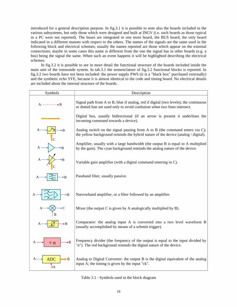
Symbols Description
Signal path from A to B, blue if analog, red if digital (two levels); the continuous or dotted line are used only to avoid confusion when two lines intersect. Digital bus, usually bidirectional (if an arrow is present it underlines the incoming command towards a device). Analog switch on the signal passing from A to B (the command enters via C); the yellow background reminds the hybrid nature of the device (analog / digital). Amplifier, usually with a large bandwidth (the output B is equal to A multiplied by the gain). The cyan background reminds the analog nature of the device. Variable gain amplifier (with a digital command entering in C). Passband filter, usually passive. Narrowband amplifier, or a filter followed by an amplifier. Mixer (the output C is given by A analogically multiplied by B). Comparator: the analog input A is converted into a two level waveform B (usually accomplished by means of a schmitt trigger). Frequency divider (the frequency of the output is equal to the input divided by "n"). The red background reminds the digital nature of the device. Analog to Digital Converter: the output B is the digital equivalent of the analog input A; the timing is given by the input "ck".
Table 3.1 - Symbols used in the block diagram
÷ n
A B
A B
C
A B
ADC
A B
A B
A C
B
A B
C
A B
A B
A B
ck

20
Fig.3.2 - The ionosonde main unit functional diagram
90° shifter
Tx Oscillator
125MHz Reference Oscillator
CRF (to PWA)
Trigger Generator
÷ 12
Code 1 Generator
Programmable Counters
Impedance Adapter
Code 2 Generator
AMP trig (to PWA)
CODE
30µs clock
400kHz_CK (400k)
C1/C2 toggle
CTM
40MHz Oscillator
Rx Oscillator
÷ 10
÷ 10
1P6T switch
SWF
FSY
RCV
÷ 2
÷ 2
RAM Addresses Generator
ADC (I)
ADC (Q) RAM (Q)
RAM (I) ADC
PC Bus (to PC / BCT board)
DSP Bus (to PC / DSP card)
36.9÷55.9 MHz
40 MHz
4 MHz
1÷20 MHz
TF#1
TF#2
TF#3
RF echo
(from Rx
antenna)
Rx on/off
FRF
RF#1 @IF#1
RF#3
LO#1 LO#2 LO#3
RF#2 @IF#2
IF#3
200kHz
100kHz
Q_CK
I_CK
Data out (8 bit)
LBI RFF
NBS RFF
Local bus
AMP trig C1/C2
400k
400k

21
All boards will be described in the following sections; at first there will be a general description (referring to fig.3.2); a more detailed description will be carried out in the second part of each section, referring to the electrical scheme, with the purpose of describing remarkable situations. The sequence of the paragraphs is established in order to follow the path of the signals from their generation to their processing. In tab.3.2 the main characteristics of the boards are summarised. Unless differently stated all analog lines are matched on 50 ohms impedance, all digital levels are TTL compatible. Tab.3.3 reports the power absorption of the subsystems, tab.3.4 the mechanical characteristics.
Board Parameter Values FSY 125 MHz (fref) reference oscillator stability 15 ppm (0°÷70°) + 1ppm per year FSY Rx Oscillator output frequency (LO#1) 36.9÷55.9 MHz FSY Tx Oscillator output frequency 1÷20 MHz FSY DDS oscillators frequency resolution 4·10-9 of fref (30 mHz) FSY CRF output level -12 dBm FSY TF#1 center frequency / 3 dB bandwidth / min. attenuation 46.4 MHz / 28 MHz / 2 dB FSY TF#2 center frequency / 3 dB bandwidth / min. attenuation 40 MHz / 5 MHz / 5 dB FSY TF#3 center frequency / 3 dB bandwidth / min. attenuation 4 MHz / 500 kHz / 8 dB FSY LO#1÷3 output level +11, +8, +5 dBm CTM pulse compression 16 bit bi-phase complementary codes CTM sub-pulse duration 30 µs CTM CODE 1 / 0 / Tx off voltages +1 / -1 / 0 V PWA RF Power Amplifier max. gain / 3 dB band limits 68 dB / 0.5÷50 MHz PWA RF Power Amplifier max. output / max. linear output +54 dBm / +53 dBm PWA RF Power Amplifier max. spurious level (linear) -14 dBc @16MHz, -27 dBc @ 2 MHz PWA RF Tx residual output power out of transmission SWF LBI RFF pass band / insertion loss 1 ÷ 25 MHz / 3 dB SWF Rx on/off switches attenuation during Rx / Tx 3 dB / 25 dB SWF 1P6T insertion loss / min. isolation 1 dB / 38 dB SWF NBS RFF central frequency 1.3 - 2.2 - 3.3 - 6.0 - 10 - 17 MHz SWF NBS RFF 3 dB bandwidth 0.6 - 1.1 - 1.8 - 3.0 - 5.0 - 8.5 MHz SWF NBS RFF typ. insertion loss 2 dB SWF Overall SWF gain / attenuation during Rx / Tx 8 dB max. / 36 dB typ. RCV RF#1 center frequency / 3 dB bandwidth / attenuation 35.9 MHz / 2.5 MHz / 5 dB RCV RF#2 center frequency / 3 dB bandwidth / attenuation 4.1 MHz / 200 kHz / 4 dB RCV RF#3 center frequency / 3 dB bandwidth / attenuation 100 kHz / 66 kHz / 4 dB RCV Variable gain amplifier dynamics / resolution 30 dB / 2 dB RCV Overall RCV board gain (0 dB attenuation) 52 dB ADC ADC input range 1.55 ÷ 3.26 V ADC ADC resolution 8 bit = 6.7 mV ADC sampling rate 100 kHz ADC oversampling factor (samples per sub-pulse) 3 ADC demodulation system synchronous with quadrature carriers DSP input data stream 290 ns per sample (16 bit) DSP processor speed 40 MIPS - 80 MHz
Tab.3.2 - Functional blocks characteristics summary
Subsystem Power (W) Main unit 28 PC (+monitor) 76 PWA (full power) 329 PWA (stand-by) 306 Overall system (full power) 433
Tab.3.3 - Power absorption
22
Subsystem H x W x D (mm) weight (kg) Main unit 133 x 483 x 300 9 PWA 267 x 483 x 490 35
Tab.3.4 - Mechanical characteristics
(H: height, W: width, D: depth)
3.2 Frequency Synthesis Board (FSY)
3.2.1 FSY functional description This board can be considered as the "heart" of the system, because it creates the timing reference for all the
other boards, both analog and digital. The analog outputs are the three sinusoids used as local oscillators outputs, the digital one is a 400 kHz clock that is used in other boards as the reference for every timing. Referring to fig.3.2, it is possible to note that all waveforms are based on the 125 MHz oscillator that outputs a two levels waveform which acts as a clock for three oscillators: the Rx, the 40 MHz and the Tx. Each of them is based on a DDS device, i.e. a digital device, programmable via a parallel or serial input, by means of which it is possible to set frequency and phase of the sinusoidal output; the output is a multi-level voltage, with so many levels to be very similar to an analog waveform. Having the need of pure sinusoid outputs, they are filtered by means of the filters named TF#1÷3. One of the oscillators (40 MHz) has the output frequency fixed, the other are programmed repeatedly when sounding, in order to generate the proper sounding frequency both in Tx and in Rx.
Without the DDS technique, it would have been necessary to generate the Tx and Rx frequency together, extracting one from the other, properly shifting the frequency of the "son" with respect to the "father", but preserving a phase coherence. With the DDS it was possible to generate the two sinusoids into two separate oscillators, being the phase coherence achieved by the common 125 MHz reference. It is worth remembering that, even in the case the frequency generated is not exactly the one chosen for the sounding (within some hertz) it has not relevant consequences if it is possible to maintain the tuning frequency of the receiver exactly locked to the transmitted one. Anyway, the DDS resolution is well beyond the one requested by the ionosonde design, while its precision is determined by the precision of the 125 MHz reference. The output frequency of the oscillator is not limited to the values in tab.3.2, it could be varied via software with the only limitation of 125/2= 62.5 MHz maximum frequency; this limits the maximum Tx frequency to 26.6 MHz, which is not planned for the actual instrument though it could be requested in a future development.
The Tx oscillator output is fed to a mixer, whose LO input is the digital code generated into the CTM board. The code activates the mixer in a digital manner (but it is a analog-like signal, matched on a 50 ohm line), so that the carrier at its RF input is output with a 0° or 180° phase according to the +1V or -1V code element. No filtering was provided because it is not essential, even though it has been planned for a future development.
The local oscillators filters TF#1÷3 are made up of an analog passive filter followed by a large band amplifier , with a fixed gain. The specification for the receiver mixers demands for +7 dBm local oscillator level, that, considering that the output of a DDS is about -7 dBm, requires at least 14 dB gain for the amplifiers. Considering the inevitable loss in the filters, a 20 dB gain IC amplifier was chosen (with DC to 4 GHz passband). This choice worked out good for all others points in which an amplification was needed (SWF, RCV). The TF#1 filter has a large bandwidth, the others a narrow one, due to the need of selecting only a fixed carrier. The TF#1÷÷÷÷3 characteristics are reported in tab.3.2.
In fig.3.2 two of the blocks "filter + amplifier" have been drawn as a single box, while the third has been split into its components because the output of the filter is used to generate other signals. In fact, the analog TF#2 output is fed to the LO#2 amplifier, but it is fed also to a comparator (it physically stays inside the 40 MHz DDS chip) to generate a digital waveform, able to be divided by ten. The 4 MHz square wave is then fed to the TF#3, which converts it back into an analog signal, and to a second by-ten divider to attain a 400 kHz clock. This signal travels into the main unit local bus and acts as a time reference for CTM, SYE and ADC boards.
3.2.2 FSY electrical scheme comments
The electrical scheme is reported in fig.A.1.1. The reference oscillator is a single part U1 in the upper left side of the scheme. The oscillators are based on the three DDS named U3 (Tx), U6 (Rx) and U8 (40 MHz). U2 and U7 are two 8 bit 8255 multiplexers, which transfer the data input to the output only if the right configuration is present at the inputs 5, 6, 8, 9, 35, 36.
The Tx mixer is U4, the resistors R1, R4 and R5 make an attenuator used for level equalisation purpose. The filters TF#1÷3 are named also on the scheme, note that the first two are shielded to increase the EMC

23
compatibility. The comparator is included inside U8, being pin 15 its input and pin 13 its output. The first divider by ten is the couple U9A + U5A, the second divider is the U5B flip flop.
3.3 Code & Timing Board (CTM) and Synthetic Echo Board (SYE). RF Power Amplifier (PWA). 3.3.1 Functional descriptions
The CTM is a completely digital board that synthesises the code and the pulse that triggers the power amplifier. The timing is derived from the 400 kHz clock generated in the FSY. It is divided by 12 to obtain a 30 µs period clock, this period is equal to a "sub-pulse" duration (see par.2.2.2). The sequence of 0s and 1s is loaded into the code generators in fig.3.2 via the PC bus, while the programmable counters generate a toggle pulse that activates the two generators alternatively; this toggle pulse is also fed via local bus to the ADC board, which sends it forward towards the DSP board via the DSP bus, in fact, the DSP must know which code has been transmitted to process the echo properly. The outputs of the two code generators are sent to an impedance adapter, that converts the two level input signal into a two level analog-like signal, matched on a 50 ohms line; in fact, this line is the input of a mixer included in the FSY, exactly its LO input.
Contemporarily, the programmable counters count a time equal to 16 sub-pulse length (or the code duration) to generate a command on the trigger generator. This last circuit outputs a 480 µs TTL pulse that acts as the enabling command for the power amplifier.
The hardware of the SYE board is almost identical to the CTM one. The only difference is in the way of working, because the codes are shifted by an amount programmable in the programmable counters. The CODE output substitutes the CODE output of the CTM and is fed to the CODE input of the FSY. The SYE board has not the AMPtrig output because the amplifier is not used in the synthetic echo mode. An integration of the two boards, CTM and SYE, in a unique board in a future development of the ionosonde is planned.
The RF Power amplifier was purchased externally to INGV, but a little modification was implemented to improve the suppression of RF power when the system is out of transmission. In fact, once the transmission is finished no RF power must be output on the air; this could be accomplished by the mixer in FSY, that does not output energy when its LO input is at zero volt. Actually, a little amount of energy passes through it even in this case, so an additional protection was added inside the PWA: a control line that disables the power supply of the active devices in the PWA, it is commanded by the AMP trig output of the CTM.
The subsystem is internally constituted by a cascade of two amplifiers: a pre-amp and a power amp; a power supply unit completes the PWA. The amplifier should work as a class A (linear) amplifier, so dissipating a large amount of power even in no transmission condition; the substitution of a different class amplifier is foreseen for future developments (an estimation gives more than 200 W power saving). The PWA was tested to evaluate its features and it was found it has not a very good linear characteristic, nor it is used with a special concern about this feature. The main characteristics of this subsystem are reported in tab.3.2. It is possible to see that the amplifier is able to output the requested 250W power (+54 dBm), even though this level is reached in saturation condition, i.e. producing a high level of harmonics and spurious.
3.3.2 CTM & SYE electrical schemes and timings comments
The CTM board scheme is reported in fig.A.1.2, that was split into two sections; the timing diagram is fig.A.2.1. It is worthy remembering that the buses named "data" and "control" are used to indicate the different lines in the PC bus in fig.3.2 (orange line). The by-12 divider is implemented by the U15 flip flop, that outputs the 30µs clock used on the board (signal [0]).
U14 (8254) makes the programmable counter, together with some circuitry (U3A, U4B, U7AB). It includes three programmable counters. The monostables in U7 ensure the pulse output by the counters have the proper duration. Counter 0 determines the main PRF (signal [2]), whose period includes the generation of the two codes C1/C2. Counter 2 is triggered by the negated output of counter 0 (signal [3]) and determines the interval between the two codes (signal [4]). The last counter 1 determines the duration of a single transmitted pulse (a multiple of the sub-pulse duration); it is triggered by a combination of the output of counters 0 and 2 (NAND of [5] and [6] gives [7]). It is used as a trigger for the ADC (signal [8]= Tx off) and the PWA (signal [10]= Tx on). All counts start as soon as the number to count is loaded (there is not a starting gate). The block called "trigger generator" in fig.3.2 is actually a set of ports (U9BC, U4CD) that make the signals [8] and [10] available as external outputs; moreover, a PC control (ON_OFF line, from U12 pin 14 to U4C pin 9) is added to disable the AMPtrig output at the end of a sounding.
The code generators are composed by all the parts in the left side of the figure A.1.2a. There are two multiplexers (as in the FSY), namely U5 and U12 (type 8255), which store the code sequences. One of them (U5) is used also as an interface between the PC and the local bus for the status signals (foreseen but not used in the present version). The parts U2+U6 (code1) and U11+U13 (code 2, all of them LS165), use the outputs of U5 and
24
U12 making them serial; their clock is the negated time base (signal [1]). The monostable outputs (signals [5] and [6]) are used to give rise to the C1/C2 toggle (signals [9] and [11]), which is used also in other parts of the system.
In the section b of the figure there is only the impedance adapter. To be precise in the impedance adapter should be included also the parts U1AB and U4A, because the C1/C2 toggle signal controls those parts, which act as a combiner for codes 1 and 2 (signals [12] and [13]), and at their output there is the stream of the two codes (signal [14]). The intermediate outputs [15] and [16] are used as negated inputs to the differential amplifier U16, which outputs the final analogue signal [17]. Note the system used to generate the double level output starting from a single level input (from 0-1 V to –1 +1 V), that makes use of a couple of exclusive ORs, allowing at the same time a gating controlled by the Tx on signal, in fact when Tx on becomes false the signals [15] and [16] become equal and their difference cancels.
About fig.A.1.3, which represents the SYE board (timing in fig.A.2.2), it is possible to see the almost identical composition with respect to CTM. One of the differences is the presence of the dip switches in the left side of section a, this because it was available no more address space in the PC bus to select peripherals, so a number of DIP switch with their pull-down resistances was adopted, considering that there is not an actual need to program the code every time. Another difference with respect to CTM is the additional monostable U20, that is used to delay the counting of U14 first counter; in fact when simulating the echo, the counting has to start from a precise moment, given by the C1/C2 toggle. The first U14 counter is used in a different manner with respect to the one in the CTM, in fact it is used to adjust the delay as much as it is chosen by the user. The signal C1/C2 was chosen because it is the only one that makes it possible to generate the synthetic echo with the code C1 or C2 accordingly to the one that would have been transmitted by the CTM (the DSP uses the C1/C2 signal to perform the correlation with the right code).
3.4 Switching Filters Board (SWF)
3.4.1 SWF functional description Just at the input of the receiving section of the ionosonde the signal coming from the Rx antenna is fed to a
Large Band Input RF Filter (LBI RFF in fig.3.2). After it there is a switch whose task is to disable the reception during transmission. A control signal is brought to the switch via the PC bus, it is synchronised with the AMP trig output by CTM.
After the Rx-on-off switch there is a one pole - 6 through switch (1P6T), it has to send the signal only to one of six pass band filters (Narrow Band Selection RF Filters - NBS RFF); they act as band selector at RF level, i.e. they limit the input signal band to reduce the noise and to avoid the image interference. To restrict the band as much as possible a multiple filter solution was adopted, each filter being easily selected by the 1P6T switch. The selector has a 38 dB isolation (when no filter is selected at the end of the sounding or when a different band is selected).
After the selectable switches an amplifier (the same type already seen in FSY) ad a second Rx-on-off switch prepares the signal before the first frequency conversion to be carried out in RCV.
3.4.2 SWF main board comments
Fig.A.1.4 reports the scheme of the main SWF board. It is a support for the many filters included in it. U1 is the connector towards the PC bus; JP1 is the connector used to settle the LBI filter, JP2÷7 are used for the six NBS filters. U2 and U3 make the 1P6T switch; this device works in a slight different manner with respect to which is deduced from fig.3.2; actually the signal does not pass through the switch (as it appears in fig.3.2) but it is present on the six filters inputs contemporarily; U2, U3 prepare a set of lines able to select one of the six filters, so that the signal passes only through one of them.
The circuitry on the lower side of the scheme is used to implement the second on-off Rx switch (the first is on the LBI circuit). The switching is accomplished by means of the Q1, Q2, Q3 FETs, which are polarised in order to be saturated (low resistance) or interdicted (high resistance): Q1 and Q2 together and Q3 in opposite way.
3.4.3 SWF LBI and NBS RFF electrical schemes
Fig.A.1.5a represents the LBI filter. It is a band pass filter, which had to be designed as high order to accomplish a large bandwidth together with steep transitions to the rejected bands. In the right side of the schematic there is the first Rx-on-off switch, made up by the Q1, Q2, Q3 FETs. The D1, D2 on the input protect against overvoltage.
In fig.A.1.5b a typical structure of a NBS filter is reported. Specifically, the actual values of the capacitors and the inductors refer to the 3.3 MHz filter; the other filters have all the same structure with different part values. The couple of diodes on the input and on the output act as switches; they are polarised by the Q1 BJT, controlled by a digital signal coming from U2, U3 on the main board.

25
3.5 Receiver Board (RCV)
3.5.1 RCV functional description This board has mainly the task of amplifying the signal and translating its frequency in the three IFs
determined in the design phase. So, a cascade of three functions is repeated thrice: a mixing, a filtering, an amplification. The mixers and the amplifiers are all similar to those included in FSY; having each mixer about 5 dB insertion loss and each amplifier 20 dB gain. The filters are obviously different and their characteristics are reported in tab.3.2 as RF#1÷÷÷÷3.
Just before the last conversion from IF#2 to IF#3 a variable gain amplifier is placed; it is exactly a variable attenuator followed by the usual 18 amplifier. The attenuator can be programmed via the PC bus and it is able to attenuate the input signal from 0 to 30 dB with a 2 dB step. This device is used only in a static way, i.e. its attenuation is set at the beginning of a sounding and it is left fixed. The output of the receiver at IF#3 is fed to the ADC for conversion.
3.5.2 RCV electrical scheme comments
Fig.A.1.6 reports the scheme of the RCV, on which it is possible to follow quite easily the signal path. On the upper left corner there are two inputs, corresponding to FRF and LO#1 signals. A mixer (U1) follows, then there is the RF#1 filter+amplifier. U2 performs the second conversion, using the LO#2 input and providing the input to the following RF#2 block. After it there is the variable attenuator, accomplished by U4; it is controlled by the set of diodes D1÷D8 and by the comparators included in U7, U8. This circuitry, together with U9, was adopted because a digital level adaptation was needed. After the attenuator there is one more amplifier (A4), the last mixer (U3) and the third filter+amplifier block RF#3. Note that RF#1 and RF#2 were shielded for more effective EMC. U6 is a voltage regulator, used because a -5V supply voltage was needed on this board.
3.6 ADC Board (ADC)
3.6.1 ADC functional description The analog signal at IF#3 is sampled and converted by a couple of 8 bit Analog-to-digital converters. As
stated in 2.3.4 two converters are needed in order to accomplish a complex FFT (ADC(I) and ADC(Q) ). They need a couple of clock signals at 100 kHz phase shifted by 90° one with respect to the other. In fig.3.2 the blocks put on the left side inside the ADC are devoted to this aim. The 400 kHz clock is divided by two twice; then a combinatory network (90° shifter) with the 200 and 100 kHz products furnishes the two requested clocks. The duty cycles are not at 50% but this is not relevant, being important the distances between two rising edges of the waveforms.
The acquired data are stored temporary into two 8k RAMs (RAM(I) and RAM(Q) ) (only 512 bits are used). The addresses both during writing and reading are generated by the "RAM addresses generator" that is simply a counter. During the writing phase the counter is triggered by the "AMP trig" signal and its clock is obviously the same of the ADCs (100 kHz). Once the storing of the 512 samples is completed the counter receives a control pulse by the DSB (via the DSP bus) and, controlled only by the DSP, starts again the addressing of the RAMs, now letting the reading of data.
Considering the typical attenuation inserted in RCV (8 dB) and a typical 50 dB overall gain for the receiving chain, a -85 dBm minimum input signal yields an ADC input of 11 mVpp, corresponding to 1÷2 resolution steps; this is in good accordance with the actual behaviour of the system, that is able to manage such weak signals in a low noise environment. On the other side of the dynamic range, the ADC maximum input signal corresponds to -41 dBm input to the receiver. Beyond this level the system continues working, but without providing further increasing in the output; the decoding capabilities are maintained but the system is not able to measure the input power.
3.6.2 ADC electrical scheme and timings comments
The ADC board schematic diagram is reported in fig.A.1.7, while the timing diagram is in fig.A.2.3. U2A and U2B implement the two by-two dividers, which have to furnish the 200 and 100 kHz clocks (signals [1] and [2] starting from [0]). The 90° shifter is simply realised by the ports U5AB, U8BD, the outputs are the AD clocks (signals [4] and [5]); the actual converters devices are U1 and U16 (TDA8703).
The converted data are fed to the two RAMs U6, U15, addressed by the "address generator", made up by the counters U10, U12 and U14, connected in cascade (they count down from 512 to 0). When data are stored, the address generator is clocked by the 100 kHz internal clock, fed to pin 4 of U10 (signal [4]); when the acquisition

26
ends, the counters are reset, a trigger is sent to the DSP (DSP BIO line), so the DSP takes the control of the address generator, sending a different clock (pin 15 of U7, corresponding to a single address line on the DSP bus). The DSP BIO pulse [10] is created by the monostable U13A triggered by the pin 13 output of U14.
The flip flop U11A on the left is activated by the Tx-on-off signal [6] corresponding to the end of transmission that starts the acquisition; at its end it is reset and the clock of the counters is switched (note the two signals [7] and [8] that enable the two different clocks alternatively). The flip flop remains in its reset state until the next Tx pulse.
At the end of the data loading on the DSP the address generator sends again the DSP BIO, so the DSP can start its internal processing. U3 and U7 are latches between the internal data lines and the DSP data bus. The set of resistors and capacitors at their outputs are used to minimise noise pickup on the lines.
U7 is a multiplexer that decodes its inputs coming from the DSP address lines A0÷A3. One of the output is the memory reading clock, another one is the enabling input of U18, whose task is to pass the toggle C1/C2 to the DSP. The ports U9 and U5C are used to generate a pulse which acts as a handshake control needed by the DSP to work properly.
The voltage regulator U19 on the lower left was used to have a cleaner +5V power supply with respect to the one coming from the PWS.
3.7 Bus Control Board (BCT) and the main unit buses (BUS)
3.7.1 BUS and BCT functional description The BUS board is a special board, that is not placed in the main unit in the same way the other boards are; in
fact it is not accessible from the front side but it acts as a common rear panel on which all the other boards connect by means of the same type of 64 pin connector. In fig.3.1 it is possible to note three different buses; they were drawn as separate buses for expositive purpose, actually they all stay on the same board. The three buses were separated to highlight that some lines are used for the communication between the main unit and the PC bus (these have been called "PC bus" on the main unit, even though they are not directly connected to the PC ISA bus), other lines are directly connected with the DSP board (DSP bus), last some lines are used only to exchange signals among the boards of the main unit and have been called "local bus". The names of the signal on the buses are reported in tab.3.5.
Local bus 14 bits 400kHz_CK Primary clock C1/C2 Code type RX_on/off Reception on RX_on/off Reception off
SyS#0÷7 System state lines (not used) TX_on/off Transmission on (if high) TX_on/off Transmission off (if high)
DSP bus 7 address bits + 16 data bits DSP_A0÷ A3 Address lines available into the DSP DSP_D0÷D15 DSP acquired data DSP_BIO DSP interrupt line DSP_IS I/O signal DSP_WAIT DSP control line PC bus 14 address bits + 8 data bits PC_A0 PC encoded address line PC_A1 PC encoded address line PC_CS#1÷8 Ionosonde devices address lines PC_D0÷D7 Buffered PC data lines PC_INT PC interrupt signal PC_RD PC read line PC_RESET Ionosonde reset (some devices) PC_WR PC write line
Tab.3.5 – BUS signals

27
The Bus Control Board (BCT), placed inside the PC, is a sort of buffer between the PC ISA bus and the bus used by the main ionosonde unit. The board reads the data on the ISA bus (they are determined by the high level PC program) and decodes them in order to address properly the boards on the main unit: program the frequency on the DDSs, generate the code, determine the attenuation in the receiver, etc.
The main unit PC bus has 8 lines for data transfer and 14 lines for addressing and controlling. The DSP bus has 16 lines used for data transfer and 7 for addressing and controlling. The main unit local bus has 14 lines. Not all of the lines on the local bus are used but they have been included to comply with possible future developments. Besides the 59 lines just mentioned, some more line is devoted to the power supply distribution (from PWS to the other boards).
3.7.2 BUS and BCT electrical scheme comments
In fig.A.1.8 it is possible to see the electrical scheme of the BUS board. It is very simple, consisting only in a series of connections among connectors. In fact the 15 connectors correspond to the actual connectors available into the ionosonde main unit. The connector on the upper left (JP1) corresponds to the ADC which requires different wiring, directly with the DSP board. The little connector on the right (JP2) gets the power supply, coming from PWS.
Fig.A.1.9 reports the electrical scheme of the BCT board. It interfaces with the PC ISA bus (connector J1) and with the external world (connectors P1 and JP3), i.e. the ionosonde main unit. U1, U2 and U3 are latches used to decouple the two buses. Being in the PC the address space reserved to external user-built peripherals at fixed address, it is stored by means of the switch S1. U7 compares the upper part of the incoming address word with the settled value to enable U6. Note that, together with the upper side of the address (PCA5÷PCA9) another line is used to check the proper call to the external peripheral: AEN (pin 6 of U3). Moreover, U6 is enabled only if one more signal is present contemporarily: it is "G2" on its pin 4; it is the output of the port U8A (on the upper side of the scheme), and become true if one of the read or write lines on the PC bus is true. By means of this enabling system it is possible to avoid that every word present on the lower side of the address lines passes through the ionosonde. Once enabled, U6 decodes the address furnished by PCA2÷PCA4, making one of the eight outputs to become active and selecting a device inside the ionosonde main unit. The PCA0 and PCA1 lines are not controlled and they are used for additional addressing, provided the right chip select is activated. On the upper left side of the scheme it is possible to see the U4 latch, not used at present, but only foreseen for future developments, to enable one interrupt request to be sent from the ionosonde to the PC. There is also a reset line controlled by the PC, that can send a reset pulse on the ionosonde bus (it is used, for example, by the 8255 multiplexers on the FSY board).
3.8 The power supply board (PWS), DSP board (DSP) and the PC About the PWS board, it is xxx model xxx. It has a triple output, at +12, -12 and +5 V, with 6A available
current ad 5V and 2A at 12V. It needs to be supplied by the main line at 220 V 50 Hz AC (like the others subsystems: PC and PWA). Three leds are present on the front panel to show the presence of the three output voltages.
A block diagram of the DSP board is reported in fig.3.3. The board is the Dalanco Spry model 5000, its most significant features are summed up in the following list: * based upon the Texas Instruments TMS320C5x series fixed point DSP (80 MHz), * up to 40 MIPS performance, * intelligent data acquisition for 8 input channels at an aggregate sampling rate of 500 KSPS, * 500 KSPS 12 bit A/D Converter, * two analog outputs (12 bit D/A), * buffered digital I/O expansion (16 bits) + serial I/O, * 64K words program RAM, * 128K words data RAM, * ISA bus interface.
The board is a little computer with many typical features, like IO devices, RAM, etc. Not everything
available has been used in the ionosonde application, specifically the RAMs and the digital IO in the lower side of the figure were used (besides the processor!). The DSP is programmed in a custom assembly language, and it makes it possible to speed up operations that would require by far longer times to be completed in a general purpose machine. As it will be explained better in the next sections, the PC has control only over general settings of the system, the start/ stop of sounding, the displaying and storing, all the other processing tasks are assigned to the DSP, including filtering, correlation and integration. More detailed information about the DSP characteristics are available in the device manual, provided by the manufacturer.
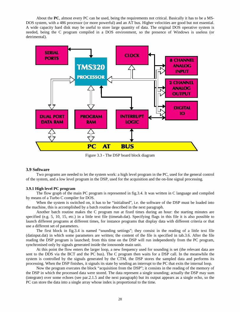
28
About the PC, almost every PC can be used, being the requirements not critical. Basically it has to be a MS-DOS system, with a 486 processor (or more powerful) and an AT bus. Higher velocities are good but not essential. A wide capacity hard disk may be useful to store large quantity of data. The original DOS operative system is needed, being the C program compiled in a DOS environment, so the presence of Windows is useless (or detrimental).
Figure 3.3 - The DSP board block diagram
3.9 Software Two programs are needed to let the system work: a high level program in the PC, used for the general control
of the system, and a low level program in the DSP, used for the acquisition and the on-line signal processing.
3.9.1 High level PC program The flow graph of the main PC program is represented in fig.3.4. It was written in C language and compiled
by means of a Turbo C compiler for DOS. When the system is switched on, it has to be “initialised”, i.e. the software of the DSP must be loaded into
the machine, this is accomplished by a batch routine described in the next paragraph. Another batch routine makes the C program run at fixed times during an hour: the starting minutes are
specified (e.g. 5, 10, 15, etc.) in a little text file (timetab.dat). Specifying flags in this file it is also possible to launch different programs at different times, for instance programs that display data with different criteria or that use a different set of parameters.
The first block in fig.3.4 is named “sounding settings”; they consist in the reading of a little text file (datinput.dat) in which some parameters are written; the content of the file is specified in tab.3.6. After the file reading the DSP program is launched; from this time on the DSP will run independently from the PC program, synchronised only by signals generated inside the ionosonde main unit.
At this point the flow enters the larger loop, a new frequency used for sounding is set (the relevant data are sent to the DDS via the BCT and the PC bus). The C program then waits for a DSP call. In the meanwhile the system is controlled by the signals generated by the CTM, the DSP stores the sampled data and performs its processing. When the DSP finishes, it signals its state by sending an interrupt to the PC that exits the internal loop.
Now the program executes the block “acquisition from the DSP”; it consists in the reading of the memory of the DSP in which the processed data were stored. The data represent a single sounding; actually the DSP may sum (integrate) over some echoes (see par.2.1.5 and the next paragraph) but its output appears as a single echo, so the PC can store the data into a single array whose index is proportional to the time.

29
Fig.3.4 – Main PC program flow chart
DSP INTERRUPT
?
ACQUISITION FROM DSP BOARD
MEAN VALUE AND ENERGY
CALCULATION
SOUNDING SETTING
SOUNDING
COMPLETE?
NEW FREQUENCY SETTING
STOP DSP &
STORE IONOGRAM
START DSP PROGRAM
GRAPHIC THRESHOLD
EVALUATION &
GRAPH
NO
YES
YES
NO

30
The next block is the “mean value and energy calculation”. Some evaluations on the acquired stream of data
are carried on. At first the mean value of the array is calculated, then a sort of energy is evaluated; actually the sum of the absolute differences of the data with respect to the mean value is calculated. This is not exactly the energy but it is a merit figure proportional to the amount of noise received along the trace. These values (average and “energy”) are used in the next block, “graphic threshold”, in fact the parameter read at the program start fixes a threshold used to output a point on the screen. The threshold is calculated dividing the “energy” previously determined by the factor read from the file; only the values in the array of data whose difference from the average overcomes the threshold are displayed on the screen as white dots; those between the threshold and its half are displayed as grey dots; those lower one half of the threshold are not displayed at all. All these operations correspond to a determination of the probability distribution of the received samples. The theoretical assumption is that most of the received samples are due to noise and only one (or very few ones) corresponds to an actual echo. The threshold is determined in order to let only very few values to be displayed, those which are the strongest (which lie on the tail of the probability distribution); at the same time the threshold is adjusted trace by trace, making the system adaptive to the background situation. No theoretical study about the threshold was carried on, in other words it is not known the relationship between the threshold and the probability distribution of the acquired values, so the determination of the most suitable value for the input parameter was carried on a heuristic basis.
At the end of the external loop the program checks for the completion of the sounding, i.e. the last programmed frequency was outputted. If the answer is no a new frequency is set, if yes the DSP is stopped and the program ends after having stored the acquired ionogram on the hard disk in a file with a fixed format and name. The name contains the julian day of the year, the day of month, the hour and the minute at which the sounding was performed. Inside it there is a header which contains all the parameters used by the programs (included the DSP). A set of strings follow; each string refer to a different frequency of sounding, and it is composed of 150 bytes, one for each sample; each byte is the colour code of the dot displayed on the screen (black, grey or white). In this way some information about the energy of the echoes is lost, but this was not considered fatal, also because of the absence of calibration of the receiver; improvements are possible in future realisations of the system. On the other hand, this kind of storage of data is useful because it simplifies the reading of data by means of other programs (for example to perform an automatic interpretation of ionograms).
Parameter (unit) Limits Start frequency (MHz) >= 1.50 Stop frequency (MHz) <= 10.00 Frequency step (MHz) 0.10 or 0.05 Internal Rx attenuation (dB) 6 ÷ 30 Pulse repetition rate (Hz) < 33 Time interval between C1/C2 pulses (ms) 15 Graphic threshold factor -- Synthetic echo height (km) 90 ÷ 600 (0 if not used) External Rx attenuation (dB) --
Tab.3.6 – Main program parameter file contents
(each parameter must be inserted in a different line, after it there is a comment string with no spaces)
3.9.2 Low level DSP program The flow diagram of the DSP program is represented in fig.3.5. It soon appears to be more complex than the
high level one; in fact the DSP has to perform both the acquisition and the signal processing, except the statistical treatment, accomplished by the C program as it was seen.
The program is written in a low level assembler language, proper of the DSP device used. As it was stated in the previous paragraph the program is to be loaded into the DSP board when the system is switched on. A batch procedure affords this task, reading at the same time a little text file which includes some parameters the user may want to change occasionally. The file name is dspinput.dat; the parameters are: the number of integration cycles to be performed, a couple of constants used to compensate for residual bias in the ADC board (kI and kQ, one for each I and Q channel), a magnification factor used by the FFT algorithm, a couple of hexadecimal numbers that express an amplitude limit to the spectral components of the received signal.

31
Fig.3.5 – DSP program flow chart
Start
Is code info. = Code1 ?
Read Code info - Read 512 Words From the ADC Board
Separate I and Q samples. Subtract kI and kQ.
Convert the Integers to Fixed Point Integers.
Complex Fourier Transform
Filter
Correlation for Code 1
Reset Integration Memory Locations. Reset Integration Counter.
Correlation for Code 2
Sum of the Correlation
Integration
Complex Inverse Fourier Transform Time Domain Amplitude
Interrupt PC
Is Integration Counter = Integration
Initialise DSP - Reset Integration Memory Locations - Reset Integration Counter
Yes
Yes
No
No
Increment Integration Counter
Is BIO Low?
No
Yes

32
When the program is launched (by the PC, see the previous par.) some registers are initialised, the processor
waits for a signal coming from the ADC, the “BIO”; in fact the ADC makes the BIO line to become high when it ends the acquisition of the echo samples, so they can be read. The DSP reads the ADC memory, together with the status of a line encoding the code (high= code 1, low= code 2). The next steps are to separate the I and Q samples, subtract the constants kI and kQ and to convert the integers into a different format (the “fixed point integers”). This last operation allows multiple operations (included the great number of multiplications in the FFT) without going into overflow condition. Actually the integers are thought as they were in absolute value less than one; the 8 bit values are converted into 16 bit numbers to be stored into the 32 bit registers of the DSP multiplier. After those preparing steps the FFT is performed. The I and Q samples are treated together as samples of a complex signal, so the Fourier transform to be calculated is the complex one, outputting a not symmetrical spectrum.
When the spectrum of the received signal is available the filtering described at the end of 2.1.5 is carried out. At first the bandwidth is slightly reduced, to make more effective the band limiting of the last IF filter. Then a hard amplitude limiting is performed on the spectral lines that exceed a fixed threshold (the one specified in the parameter file). When a single line exceeds the threshold its value is put to zero (both the real and imaginary part). The threshold has been determined by trials and can be modified accordingly to the noise environment, that may change in time and space.
Once the spectrum is obtained the correlation with the code is performed, in the frequency domain (it is a simple multiplication sample by sample). Obviously the correlation has to be done with the proper code, correspondent to the one used to obtain the last acquired signal; that is the reason of the check of the code in the centre of the diagram. If the code used is the first, all the previous operations have to be repeated to process the second one. After having acquired both codes they can be summed to make effective their complementary nature.
The next step is the integration, and it consists only in the accumulation of the traces into the same array, until the integration counter reaches the specified number. It only at this point that the inverse Fourier transform is executed. As a consequence of the various processing of the signals, the output is complex, with I and Q components, so the extraction of the amplitude must be carried on. If the processing were performed in the time domain the extraction of the amplitude should have be done at first, in our case it is done at the end; in both cases the final output must be real.
At this point the work is almost done, and after some resetting, the DSP interrupts the PC to signal it has finished its task (see fig.3.4). The PC will read the data stored temporarily into the DSP RAM.
3.9.3 Filenames convention
The data file produced by the C program have a name that is a function of the time at which the file was generated. The convention for the names is: YYDDDHMM.ext, where: YY are last two digits of the year, DDD is a three digit number representing the calendar day (starting from Jan 1st = 1), H is a letter representing the day hour (A=0, B=1 … W=22, X=23), MM are two digits for the 00 to 59 minutes within the hour, ext is the three character extension, that is “RDF” by default, even though it is possible to generate files with a different format (and extension), but this feature is not used now. 3.10 Technology notes
Some note about the technologies adopted in the ionosonde manufacturing is added at the end of this chapter. The design has been aided by means of a professional electronic CAD, used both for some simulations and
for the implementation of the actual layout of all the circuits. Each board is a double side PCB (vetronite substratum, with a photoresist already present) on which the routing has been impressed by means of rather traditional systems: the output of the CAD is printed on slides by a laser printer, that allows for a very good resolution and a high contrast. The slides are lined up on the board and exposed to an UV rays source, so that the photoresist can be removed chemically by means of a sodium hydroxide solution (7 g/l). In the end the copper is semoved by means of a sodium persulfide (100 g/l). Summing up: where the copper traces must remain the persulfide do not act because the photoresist was not removed, this happened because of the traces on the slides that shielded the UV light. At this time the board can be perforated to settle the components.
About the components used, it is worthy to remember that both the traditional technology and the new surface mounting one have been used. So, on the boards it is possible to see traditional lumped elements (resistors, capacitors, etc.), the DIP (Dual in Line Package) integrated circuits and the SMD (Surface Mounting Device); the last are in the SOP Small Outline Packcge) and in the SSOP versions (Shrinked SOP). The SMD technology was not used only for advanced devices like. the DDS’s but also for some resistors and capacitors.

33
In the RF boards attention was reserved to EMC, adopting all the typical measures that allow improvements in the performances. For example: the filters and amplifiers were shielded, the supply lines were filtered, the analog and digital grounds were held separated as long as possible, a ground plane was created almost everywhere, etc.
In fig.A.3.3 it is possible to have a look to the FSY board, that resumes on it all the technology concepts exposed in this paragraph.
34
4. CONCLUSIONS 4.1 Test results
The ionosonde system has been tested during the last four months, producing ionograms of good quality,
comparable to the ones produced by the older ionosonde systems working at INGV and purchased externally. Some result will be presented, making comparisons with the two systems: � the old VOS-1A ionosonde manufactured by Barry Research Corporation (referred to as VOS); � the new DPS-4 ionosonde manufactured by the Center for Atmospheric Research of Lowell University of
Massachusetts (referred to as DPS). In all ionograms on the horizontal axes there are the frequencies in MHz, while the units on the vertical axes
are km; they were scaled graphically and placed in the pages in order to allow an easy comparison among scales; all soundings have been performed in the Rome ionospheric observatory.
In fig.3.1 there is the ionogram produced on May 29th, 2002, by the INGV ionosonde; in fig.3.2 and 3.3 there are the comparisons with the ones produced by the DPS and VOS respectively. The soundings were performed within few minutes around 7.00 am (local time).
In fig.3.4 and 3.5 there is another example, respectively by the INGV ionosonde and the DPS; there is no comparison with the VOS because the sounding was performed at 5.45 pm, while the VOS works only at the 0 minutes of each hour. The day was July 7th, 2002.
The ionograms showed were chosen as good representatives of the ionograms produced by the various ionosondes; the deviations from the “normal” cases like the ones shown are rare. It is possible to note the good quality of the ionograms produced by the INGV ionosonde, accompanied by a good background noise level (compare to VOS). For some conditions, the INGV ionosonde is even better than the DPS, e.g. at the lower frequencies (E layer).
Fig.3.1 – INGV ionosonde, 2002/5/29, 7am

35
Fig.3.2 – DPS ionosonde, 2002/5/29, 7am
Fig.3.3 – VOS ionosonde, 2002/5/29, 7am

36
Fig.3.4 – INGV ionosonde, 2002/7/4, 5.45pm
Fig.3.5 – DPS ionosonde, 2002/7/4, 5.45pm
4.2 Future developments
The present state of the design and development of the new INGV ionosonde is far from being definitive and
many improvements have already been identified. Here they are briefly introduced, grouping them by their connection to the various subsystems and boards.
* Main unit An external antenna switch may be useful when another ionosonde system should be operative contemporarily
to the INGV ionosonde. The switch control can be inserted inside the CTM. All the signals paths shall be checked and the amplifications revised, to improve the linearity of the overall
system. An automatic calibration circuitry can be designed, in order to choose the best set of attenuations to be inserted:
at the CRF out, at the RF in, and inside the receiver.

37
* FSY The CRF signal is not filtered; a band filter can be inserted. In order to spare address space on the BUS some of
the programmable latches can be substituted by DIP switches; this is possible because the 40 MHz oscillator has its frequency fixed. Some circuitry able to sense the presence of the proper signals generated onto the board can be introduced; the signals to be checked can be: the 125 MHz reference, the LO outputs, the CRF out, the 400 kHz clock; also the temperature in some critical spot could be checked. The checking could be accomplished even by a simple average value extractor, comparing the output with a threshold and outputting a green or red light of an LED.
* CTM Also on this board some addressing circuitry can be simplified, making the selection of the code more static
(DIP switches), but, considering that the type of code is not subjected to vary, it has not consequences on the usual working of the system.
* SYE This board can be completely avoided, being almost identical to CTM, so it can be integrated in the last, with
some little circuitry added. * PWA The power amplifier is to be substituted by a different type, that shall allow a better efficiency and a better
linearity. Experimentation on a new model has already been carried on and this can be used in the future. * SWF The layout and the shielding can be revised and made more effective. Also the input filter (LBI RFF) can be
revised. A visual system, based on LEDs, will be introduced to indicate the actual NBS RFF filted used in real time.
* RCV The variable gain could be accomplished in a different way; an AGC circuit could be introduced. * ADC, BCT and BUS, PWS : nothing to modify. * PC New and more powerful computers can be adopted. More moderns systems are more useful because they allow
easily the network connection, and this feature is important, considering that future applications include the settling of ionosondes also in sites with no operators working nearby.
* DSP and Software A new DSP board has already been purchased and tested; it will allow a greater speed. The chance of acquiring
a floating point DSP has been considered too. The software will be the “part” subjected to the more significant improvements, not because it is now of bad
quality, but because of its capability to be rapidly modified and tested. More efficient algorithms can be adopted, in order to: speed up the computing time (making possible to increase the PRF), making all the calculations more precise, reducing the “computing noise”, improve the filtering in the frequency domain (for instance using more information about the code spectrum, including the phase). Also the actual sounding absolute frequency can be varied, avoiding the coincidence with “clean” values, like 1, 2, 3 MHz and so on (to modify with, say, 1.015, 2.015, etc.).
The most interesting algorithms to be introduced should be the calibrations. An “environment noise calibration” should be very powerful: a measure of the status of all the interfering sources of noise, with the purpose of cancelling them in the subsequent sounding. A different calibration, a “system calibration” could be implemented, in order to take into account for the actual transmitted code and not the ideal one when performing the correlation.
All the modifications just examined are rather easily to implement and they do not affect the system overall
design. Deeper improvements imply the introduction of new boards and the complete rebuilding of the software. The capabilities that would be desirable to be added are: the doppler shift analysis and the ordinary and extraordinary way recognition, also a more precise measurement of the received power (i.e. the overall absorption of the ionosphere) would be useful.

38
A. APPENDEXES
A.1 Schematic diagrams The electric schematic diagrams of the boards of the ionosonde are reported from pag.39 to 49, figures from
A.1.1 to A.1.9.
A.2 Timing diagrams The timing diagrams of the digital signals on the CTM, SYE and ADC boards are reported from pag.50 to
52, figures from A.2.1 to A.2.3.
A.3 Pictures The complete ionosonde system is visible in fig.A.3.1. Other pictures are at pag.53 and 54.
Fig.A.3.1 – The complete ionosonde system

39
Fig.A.1.1 - FSY board
TRANSMITTER1_1.DSN 1.1
FREQUENCY SYNTHESIS BOARD
ISTITUTO NAZIONALE DI GEOFISICA E VULCANOLOGIA
C
1 1Monday, April 22, 2002
Title
Size Document Number Rev
Date: Sheet of
VCC
VCC
VCC
VCC
VCCVCC
VCC
VCC
VCC
VCC
VCC
VCC
VCC
VDD
VDD
VDD
VDD
VDD
VCC
VCC
CLO
CK
PCD3
A1
PCD7
CS#7
PCD2
PCD5PCD6
A0
PCD1
PCD4
PCD0
RESET
/RD
PCD0
/WR
PCD6
PCD4
RESETA1A0
PCD2
PCD7
PCD5
CS#6
PCD3
/RD
PCD1
CLOCK
CLOCK
400 kHz
PCD0
PCD7
PCD5
PCD1PCD2
PCD4PCD3
PCD6
/RD/WR
A0A1
RESET
/WR
CS#6CS#7
Vcci
400 kHz
Vcci
L1
1.5uH
L2
.33uH
C340.1pF
C4647nF
C4547nF
C3347nF
C3047nF
C3147nF
C3247nF
C3847nF
C1647nF
C1347nF
C1447nF
C1247nF
C1147nF
C2847nF
C2747nF
C2647nF
C2947nF
C368pF
R1624
U9A
74S112
3
1
2
5
6
4
15
J
CLK
K
Q
Q
PR
CL
U5B
74LS390
1512
14 13
1110
9CKACKB
CLR QA
QBQC
QD
U7
8255
3433323130292827
53698
356
432140393837
1819202122232425
1415161713121110
D0D1D2D3D4D5D6D7
RDWRA0A1RESETCS
PA0PA1PA2PA3PA4PA5PA6PA7
PB0PB1PB2PB3PB4PB5PB6PB7
PC0PC1PC2PC3PC4PC5PC6PC7
R1851
U5A
74LS390
14
2
3567
CKACKB
CLR
QAQBQCQD
U8
AD9850XRS
1234
5 6
78
910
11
12
13
1415
16
17
18
19
2021
22
23
24
25262728 D3
D2D1D0
DG
ND
VD
D
WCLKFQUD
CLK
INA
GN
D
AV
CC
RS
ET
QOUT
QOUTBVINN
VINP
DACBP
AV
CC
AG
ND
IOUTBIOUT
RESET
VD
DD
GN
D
D7D6D5D4
C2470pF
R8 3.9K
U2
8255
3433323130292827
53698
356
432140393837
1819202122232425
14151617
13121110
D0D1D2D3D4D5D6D7
RDWRA0A1RESETCS
PA0PA1PA2PA3PA4PA5PA6PA7
PB0PB1PB2PB3PB4PB5PB6PB7
PC0PC1PC2PC3
PC4PC5PC6PC7
R9 3.9K
U6
AD9850XRS
1234
56
78
9
10
11
12
1314
1516
17
18
19
2021
22
23
24
25262728 D3
D2D1D0
DG
ND
VD
D
WCLKFQUD
CLK
IN
AG
ND
AV
CC
RS
ET
QOUTQOUTB
VINNVINP
DACBP
AV
CC
AG
ND
IOUTBIOUT
RESET
VD
DD
GN
D
D7D6D5D4
U1
125MHz
1 48
14
7
11
NC
NC
OUT
VC
C
GN
D
VC
C
C15
47nF
U10C
DIN64_AC
C1C2C3C4C5C6C7C8C9
C10C11C12C13C14C15C16C17C18C19C20C21C22C23C24C25C26C27C28C29C30C31C32
C1C2C3C4C5C6C7C8C9C10C11C12C13C14C15C16C17C18C19C20C21C22C23C24C25C26C27C28C29C30C31C32
L4
15uH
L5
1uHC4100pF L8
.1uH
C6 15nF
L7
1uH
L6
15uHC5100pF
C7
26.41pF
C8
26.64pF
C9150pF
C10150pF
L1266.61nH
L1366.02nH
L10
445.5nH
L11
441.6nH
A1ERA-5
1 3
2 4
A3ERA-5
1 3
2 4
A2ERA-5
1 3
2 4
R10120
L1447uH
L15
47uH
L1647uH
R15
120
R17120
R324
R251
R141k
R131k
R1224
R1151
C22
10nF
C23
10nF
C36
10nF
C37
10nF
C42
100nF
C43
100nF
C39
47nF
C3547nF
C19
47nF
R23150
R22150
R24150
R25150
R20 39 R21 39
J5
FISCHER1
2
J4
FISCHER1
2
J3
FISCHER1
2
J2BNC
1
2
R4220
R5220
R1 24
U4TAK-5
3
1 8
2 5 64
7
IF
RF LO
GN
DG
ND
GN
DIF
GN
D
U10A
DIN64_AC
A1A2A3A4A5A6A7A8A9A10A11A12A13A14A15A16A17A18A19A20A21A22A23A24A25A26A27A28A29A30A31A32
A1A2A3A4A5A6A7A8A9
A10A11A12A13A14A15A16A17A18A19A20A21A22A23A24A25A26A27A28A29A30A31A32
C1
5-55pf
C240.1pF
C250.1pF
C440.1pF
C40 0.1pF C41 0.1pF
C170.1pF
C21
0.1pF
J1FISCHER1
2
+C1810uF
L18
100uH
R71k
U3
AD9850XRS
1234
5 6
78
910
11
12
1314
1516
17
18
19
2021
22
23
24
25262728 D3
D2D1D0
DG
ND
VD
D
WCLKFQUD
CLK
INA
GN
D
AV
CC
RS
ET
QOUTQOUTB
VINNVINP
DACBP
AV
CC
AG
ND
IOUTBIOUT
RESET
VD
DD
GN
D
D7D6D5D4
R193.9k
L317nH
L917nH
+ C204.7uF
R61k
L17
100uH
40MHz Pass Band Filter
(L3 =17.6nH)(L1+L2 = 2.3uH)(C1=7.0pF) *1
(C2+C3=900.3pF)
*1
(C4=99.5pF)
4MHz Pass Band Filter
(L4+L5 =15.9uH) (C5=99.5pF) (L6+L7 =15.9uH)
(L8+
L9 =
124.3
nH
)
(C6=12.7nF)
46MHz Pass Band Filter
*2 *2(C9=176.6pF) (C10=178.2pF)
Att.= 4dB
Att.= 6dB Att.= 6dB
*13 spire in ariadiam supporto = 3 mmdiam filo = .7 mm
*26 spire in ariadiam. supporto = 3 mmdiam. filo = 0.7 mm
Note sugli induttoriTra parentesi sono indicati i valori teoriciprovenienti dal calcolo.
LO#3 out
LO#2 out
LO#1 out
CODE in
CRF out
400kHz_CK
TF#1
TF#2
TF#3
400kHz_CK
VCC = 5VVDD = 12V-VDD =-12V
(1/2W)
(1/2W)
(1/2W)
(Shield)
(Shield)

40
Fig.A.1.2a - CTM board (1st section)
TIMING_CODE1_0.DSN (timing_code1.sch) 1.0
TIMING-CODE BOARD
ISTITUTO NAZIONALE DI GEOFISICA e VULCANOLOGIA
B
1 2Thursday, October 25, 2001
Title
Size Document Number Rev
Date: Sheet of
VCC
VCC
VCC
+VDD
-VDD
VCC
VCC
VCC
VCC
VCC
VCC
VCC
VCC
VCC
VCC
VCC VCC
VCC
VCC
TXON_OFF
TOTAL_CODE
PCD0
PCD2
PCD6
PCD7
PCD4
PCD6
PCD3
PCD0
PCD5
PCD2
/WRRESET
A1
PCD3PCD3PCD3PCD3
PCD6PCD6PCD6PCD6PCD6PCD6PCD6
/RD
PCD2PCD2PCD2
A0
PCD0
PCD5PCD5PCD5PCD5PCD5PCD5PCD4PCD4PCD4PCD4PCD4
PCD3PCD4PCD5
PCD7
CS
#1
A1
A0
/WR
PC
D7
PC
D6
PC
D5
PC
D4
PC
D3
PC
D2
PC
D0
CS#1CS#2CS#3
CS#2
CS#3
PCD1
PC
D1
PCD1
PCD1PCD1
PCD7PCD7PCD7PCD7PCD7PCD7PCD7PCD7
SYS0SYS1SYS2SYS3
SYS7
SYS4SYS5SYS6
SYS0SYS1SYS2SYS3SYS4SYS5SYS6SYS7
/RD
/RD/WRA0A1RESET
/RD/WRA0A1RESET
TX
C1/C2
/TX
ON_OFF
ON_OFF
U11
74LS165
1011121314
3456
215
1
9
7
SERABCDEFGH
CLKINH
SH/LD
QH
QH
U13
74LS165
1011121314
3456
2
151
9
7
SERABCDEFGH
CLK
INHSH/LD
QH
QH
U5
8255
3433323130292827
53698
356
432140393837
1819202122232425
1415161713121110
D0D1D2D3D4D5D6D7
RDWRA0A1RESETCS
PA0PA1PA2PA3PA4PA5PA6PA7
PB0PB1PB2PB3PB4PB5PB6PB7
PC0PC1PC2PC3PC4PC5PC6PC7
U2
74LS165
1011121314
3456
215
1
9
7
SERABCDEFGH
CLKINH
SH/LD
QH
QH
U6
74LS165
1011121314
3456
2
151
9
7
SERABCDEFGH
CLK
INHSH/LD
QH
QH
U12
8255
3433323130292827
53698
356
432140393837
1819202122232425
1415161713121110
D0D1D2D3D4D5D6D7
RDWRA0A1RESETCS
PA0PA1PA2PA3PA4PA5PA6PA7
PB0PB1PB2PB3PB4PB5PB6PB7
PC0PC1PC2PC3PC4PC5PC6PC7
U1A
74LS10
12
1312
R127K
C6
100p
R227K
U7A
74LS123
14
15
1
23
13
4
CEXT
REXT/CEXT
A
BCLR
Q
Q
U9C
74LS04
56
U4B
74LS00
456
U9A
74LS04
12
U3A
74LS74
2
3
5
6
41
D
CLK
Q
Q
PR
CL
U10A
DIN64_AC
A1A2A3A4A5A6A7A8A9A10A11A12A13A14A15A16A17A18A19A20A21A22A23A24A25A26A27A28A29A30A31A32
A1A2A3A4A5A6A7A8A9
A10A11A12A13A14A15A16A17A18A19A20A21A22A23A24A25A26A27A28A29A30A31A32
C8
100p
U7B
74LS123
6
7
910
115
12
CEXT
REXT/CEXT
AB
CLRQ
Q
U15
74LS92
141
67
121198
AB
R0(1)R0(2)
QAQBQCQD
U10C
DIN64_AC
C1C2C3C4C5C6C7C8C9
C10C11C12C13C14C15C16C17C18C19C20C21C22C23C24C25C26C27C28C29C30C31C32
C1C2C3C4C5C6C7C8C9C10C11C12C13C14C15C16C17C18C19C20C21C22C23C24C25C26C27C28C29C30C31C32
U9B
74LS04
3 4
C4100nF
C1100nF
U4D74LS00
12 1311
U1B
74LS10
345
6
C2
100nF
U4A
74LS00
1
23
J2
BNC
1
2
U14
8254
8 7 6 5 4 3 2 1 22 23 19 20 21
9 11 10 15 14 13 18 16 17
D0
D1
D2
D3
D4
D5
D6
D7
RD
WR
A0
A1
CS
CLK
0G
0O
UT0
CLK
1G
1O
UT1
CLK
2G
2O
UT2
C9100nF
C12100nF
C7100nF
C13100nF
C5100nF
C14100nF
C11
100nF
U4C
74LS00
9
108
J3BNC
1
2
C10100nF
C15100nF
C3100nF
CODE1
CODE2DATA BUS
CONTROL BUS
STATUS SYSTEM BUS
SYSTEM STATUS BUS
[ 0 ]
[ 0 ]
[ 0 ][ 1 ]
[ 1 ]
[ 1 ]
CODE 1 OUT
CODE 2 OUT
[ 2 ]
[ 3 ]
[ 4 ]
[ 5 ]
[ 5 ]
[ 6 ]
[ 6 ]
[ 6 ]
[ 7 ]
[ 9 ]
[ 9 ]
[ 8 ]
[ 8 ]
[ 10 ]
[ 11 ]
[ 10 ]
[ 12 ]
[ 13 ]
[ 14 ]
[ 2 ]
ATRG out
400kHz_CK
TXon_off
/TXon_off
/ATRG out
[ 10 ]
C1/C2

41
Fig.A.1.2b - CTM board (2nd section)
VCC
+VDD
-VDD
TOTAL_CODE
TXON_OFF
U8A
74LS86
1
23
U8B
74LS86
4
56
+
-
U16
AD848
3
26
7 14 5
R4
330
R6
330
R3
220
R7
220
C18100nF
C16
10nF
C20
10nF
+C19
10uF
+
C17
10uF
R5
51
J1FISCHER
1
2
[ 15 ]
[ 16 ]
[ 17 ]
CODE out

42
Fig.A.1.3a - SYE board (1st section)
TEST_CARD1_0.DSN (test_card1.sch) 1.0
TEST-BOARD
ISTITUTO NAZIONALE DI GEOFISICA e VULCANOLOGIA
B
1 2Thursday, August 09, 2001
Title
Size Document Number Rev
Date: Sheet of
VCC
VCC
VCC
VCC
VCC
VCC
VCC
VCC
VCC
VCCVCC
VCC
VCC
VCC
+VDD
-VDD
VCC
VCC
VCC
TOTAL_CODE
TXON_OFF
PCD3PCD3PCD3PCD3
PCD6PCD6PCD6PCD6PCD6PCD6PCD6
PCD2PCD2PCD2
PCD0
PCD5PCD5PCD5PCD5PCD5PCD5PCD4PCD4PCD4PCD4PCD4
PC
D7
PC
D6
PC
D5
PC
D4
PC
D3
PC
D2
PC
D0
PC
D1
PCD1PCD1
PCD7PCD7PCD7PCD7PCD7PCD7PCD7PCD7
TX
A0A1
CS
#8
RESET
/WR
A1
CS#8
/WR
A0
/RD
/RD U13
74LS165
10111213143456
2
151
9
7
SERABCDEFGH
CLK
INHSH/LD
QH
QH
U2
74LS165
10111213143456
215
1
9
7
SERABCDEFGH
CLKINH
SH/LD
QH
QH
U1A
74LS10
12
1312
R127K
C6
100p
R227K
U7A
74LS123
14
15
1
23
13
4
CEXT
REXT/CEXT
A
BCLR
Q
Q
U9C
74LS04
56
U4B
74LS00
456
U9A
74LS04
12
U3A
74LS74
2
3
5
6
41
D
CLK
Q
Q
PR
CL
U10A
DIN64_AC
A1A2A3A4A5A6A7A8A9A10A11A12A13A14A15A16A17A18A19A20A21A22A23A24A25A26A27A28A29A30A31A32
A1A2A3A4A5A6A7A8A9
A10A11A12A13A14A15A16A17A18A19A20A21A22A23A24A25A26A27A28A29A30A31A32
C8
100p
U7B
74LS123
6
7
910
115
12
CEXT
REXT/CEXT
AB
CLRQ
Q
U15
74LS92
141
67
121198
AB
R0(1)R0(2)
QAQBQCQD
U10C
DIN64_AC
C1C2C3C4C5C6C7C8C9
C10C11C12C13C14C15C16C17C18C19C20C21C22C23C24C25C26C27C28C29C30C31C32
C1C2C3C4C5C6C7C8C9C10C11C12C13C14C15C16C17C18C19C20C21C22C23C24C25C26C27C28C29C30C31C32
U4A
74LS00
1
23
U1B
74LS10
345
6
U14
8254
8 7 6 5 4 3 2 1 22 23 19 20 21
9 11 10 15 14 13 18 16 17
D0
D1
D2
D3
D4
D5
D6
D7
RD
WR
A0
A1
CS
CLK
0G
0O
UT
0
CLK
1G
1O
UT
1
CLK
2G
2O
UT
2
U9B
74LS04
3 4
C4100nF
U17
8x560
2 3 4 5 6 7 8 91JP1 HEADER 8X2
1 23 45 67 89 1011 1213 1415 16
JP2 HEADER 8X2
1 23 45 67 89 1011 1213 1415 16
C9100nF
C5100nF
C14100nF
C11
100nF
U21
8x560
23456789 1
JP4
HEADER 8X2
1 23 45 67 89 1011 1213 1415 16
U6
74LS165
10111213143456
2
151
9
7
SERABCDEFGH
CLK
INHSH/LD
QH
QH
U19
8x56023456789 1
C3100nF
R8
27K
C21
100p
U20A
74LS123
14
15
12313
4
CEXT
REXT/CEXT
AB
CLRQ
Q
U11
74LS165
10111213143456
215
1
9
7
SERABCDEFGH
CLKINH
SH/LD
QH
QH
JP3
HEADER 8X2
1 23 45 67 89 1011 1213 1415 16
U18 8x560
2 3 4 5 6 7 8 91
C12
100nF
C2100nF
C13100nF
C10100nF
C1100nF
C22100nF
DATA BUS
CONTROL BUS
[ 0 ]
[ 0 ][ 1 ]
[ 1 ]
[ 1 ]
CODE 1 OUT
CODE 2 OUT
[ 2 ]
[ 3 ]
[ 4 ]
[ 5 ]
[ 5 ]
[ 6 ]
[ 6 ]
[ 6 ]
[ 7 ]
[ 9 ]
[ 8 ]
[ 11 ]
[ 10 ]
[ 12 ]
[ 13 ]
[ 14 ]
[ 2 ]
[ 0 ]
[ 18 ][ 19 ]
43
Fig.A.1.3b - SYE board (2nd section)
VCC
+VDD
-VDD
TOTAL_CODE
TXON_OFF
U8A
74LS86
1
23
U8B
74LS86
4
56
+
-
U16
AD848
3
26
7 14 5
R4
330
R6
330
R3
220
R7
220
C18100nF
C16
10nF
C20
10nF
+
C19
10uF
+
C17
10uF
R5
51
J1FISCHER
1
2
ECHO out
[ 15 ]
[ 16 ]
[ 17 ]
44
Fig.A.1.4 - SWF board (main board)
FILTERBUS1_1.DSN 1.1
BUS FILTRI
ISTITUTO NAZIONALE DI GEOFISICA e VULCANOLOGIA
B
1 1Thursday, October 18, 2001
Title
Size Document Number Rev
Date: Sheet of
+VDD
+VDD V+
-VDD V-
+VDD
-VDD
-VDD +VDD
VCC
VCC
-VDD
+VDD
VCC
D0D1D2D3D4D5D6D7
D0D1D2D3D4D5D6D7
JP1
HEADER 13
12345678910111213
U4A
75188
23
U4B
75188
4
56
U4C
75188
9
108
U4D
75188
12
1311
U3
74ALS574
23456789
111
1918171615141312
D1D2D3D4D5D6D7D8
CLKOC
Q1Q2Q3Q4Q5Q6Q7Q8
U2A
7406
12
U2B
7406
34
U2C
7406
56
U2D
7406
98
U2E
7406
1110
U2F
7406
1312
D3
1N4007
Q2
2N4391
2
3
1
U1A
DIN64_AC
A1A2A3A4A5A6A7A8A9
A10A11A12A13A14A15A16A17A18A19A20A21A22A23A24A25A26A27A28A29A30A31A32
A1A2A3A4A5A6A7A8A9A10A11A12A13A14A15A16A17A18A19A20A21A22A23A24A25A26A27A28A29A30A31A32
U1C
DIN64_AC
C1C2C3C4C5C6C7C8C9
C10C11C12C13C14C15C16C17C18C19C20C21C22C23C24C25C26C27C28C29C30C31C32
C1C2C3C4C5C6C7C8C9C10C11C12C13C14C15C16C17C18C19C20C21C22C23C24C25C26C27C28C29C30C31C32
A1
MAR-1
13
24
D4
1N4007
D2
1N4007
D1
1N4007
Q1
2N4391
2
3
1
Q3
2N4391
23
1
C4
10nF
L1
150uH
R1390
C6
10nF
C5
10nF
JP4
HEADER 13
1 2 3 4 5 6 7 8 9 10 11 12 13
JP5
HEADER 13
1 2 3 4 5 6 7 8 9 10 11 12 13
JP6
HEADER 13
1 2 3 4 5 6 7 8 9 10 11 12 13
JP7
HEADER 13
1 2 3 4 5 6 7 8 9 10 11 12 13
JP3
HEADER 13
1 2 3 4 5 6 7 8 9 10 11 12 13
JP2
HEADER 13
1 2 3 4 5 6 7 8 9 10 11 12 13
C1
10nF
C2
10nF
R2100K R3100K
J2
FISCHER1
2
C3
10nF
C7
10nF
J1
FISCHER1
2
R4470
R5470
JP8
HEADER 9X2
1 23 45 67 89 1011 1213 1415 1617 18
CS #5
SS
S
DD
D
1/2 W
0
5
0
5
-12
+12
+12
-12
-12
+12
+12
-12
0
-12
-12
0
-12
0
0
-12
ANTENNA in
FRF out
RX on_off
/RX on_off

45
Fig.A.1.5a - LBI RF filter (SWF board)
Fig.A.1.5b - NBS RF filter topology (SWF board)
L14.7uH
L26.8uH
L34.7uH
L4
0.33uH
L5
0.33uH
L6
0.33uH
C1
3.3nF
C5
33pF
C9150pF
C123.3nF
C282pF
C6
68pF
C1015nF
C13
2.2nF
C16
3.3nF
C3
1pF
C733pF
C112.2nF
C14
1nF
C17
3.3nF
C4
47pF
C8
120pF
JP1
DIN41617
1 2 3 4 5 6 7 8 9 10
11
12
13
R2
100k
R1
100k
Q12N4391
2
3
1
Q3
2N4391
23
1
C18
10pFC19390pF
C15
1nF
C20
47nFR3
1k
Q22N43912
3
1
D1
1N4148
D2
1N4148
Signal INSignal OUT
-12V
0V 0V
-12V
+VDD
-VDD
+VDD
-VDD
J113 poli DIN 41617
12345678910
11
12
13
R2
2.7
R7
3.3
R13.3k
R5
1k
R6
1k
R84.7k
D1
1N4007
D2
1N4007
D31N4148
L4100uH
L3
5.1uH
D4
1N4148
L7100uH
C13100nF
C6390pF
C72.4nF
C4390pF
C12100nF
C1110nF
Q1 2N2907
L2
8.7uH
L1
5.1uH
L5806nH
C1
1pF
C3
1pF
C8
1pF
C10
1pF
C2
1pF
L6806nH
C5223.8pF
C17
1pF
R4270
R3270
C18
1pF
C14
1pF
C15
1pF
C16
1pF
C92.4nF
SIGNAL OUT
SIGNAL IN
ON/OFF CONTROL
-VDD= -12V
+VDD= +12V

46
Fig.A.1.6 - RCV board
VDD
VCC
VCC
VCC
-VDD
VCC
VDD VCC
VCC
-VDD
VDD
VDD
VDDVDD
-VCC
PCD1PCD0
PCD7PCD6
PCD3
PCD5PCD4
PCD2
400 kHz
-VCC
-VCC
C9 47pF
C18 12pF
L7
22uH
C12
47nF
C33
10nFC31 47nF
L17
180uH
L13
10uH
C29
1uF
+-
U8A
LM324
321
411+-
U7D
LM324
121314
411 +-
U8C
LM324
1098
411+-
U8B
LM324
567
411+-
U7B
LM324
567
411
D5 D8
+-
U7C
LM324
1098
411+-
U7A
LM324
321
411
D7
U9
74ALS574
23456789
111
1918171615141312
D1D2D3D4D5D6D7D8
CLKOC
Q1Q2Q3Q4Q5Q6Q7Q8
D6
C10 27pFL6
22uH
C11
47nF
J4FISCHER
1
2
J3FISCHER
1
2
J1FISCHER1
2J2FISCHER
1
2
D103.6V
C37 100nF
C23
5-50pF
L5
2.7uH
L8
2.7uH
C42
3.3nF
C26
0.1pFC28 100nF
C32 0.1pF
L14
33uH
C36 33nF
L12
6uH
L11
1.5uH
C27 15nFC34
47nF
R6A
680
116
R6B
680
215
R6C
680
314
R6D
680
413
R6E
680
512
R6F
680
611
R6H
680
89
R6G
680
710
D2
R92.2k
C24
47nF
D1
C35
47nF
C25
47nF
C210nF
D4D3
C30
1uF
L247uH
C46100nF
R5330
R3120
C200.1pF
R7
330
U3
TAK-53 1
8
256
4
7
IF RF
LOGN
DG
ND
GN
DIF
GN
DL1868uHC39
33nFC40
0.1pF
U6LM7905
3
1
2VIN
GN
D
VOUT
D9
3.6V
C38
0.1pF
+ C484.7uF
U2TAK-5
3
1 8
2 5 6
4
7
IF
RF LO
GN
DG
ND
GN
D
IFGN
D
C5347nF
R81k
L10420nH
A3
ERA-5
13
24
A2ERA-5
1 3
2 4
C19
4.7nF
L1947uH
L15390uH
U5A
DIN64_AC
A1A2A3A4A5A6A7A8A9A10A11A12A13A14A15A16A17A18A19A20A21A22A23A24A25A26A27A28A29A30A31A32
A1A2A3A4A5A6A7A8A9
A10A11A12A13A14A15A16A17A18A19A20A21A22A23A24A25A26A27A28A29A30A31A32
U5C
DIN64_AC
C1C2C3C4C5C6C7C8C9C10C11C12C13C14C15C16C17C18C19C20C21C22C23C24C25C26C27C28C29C30C31C32
C1C2C3C4C5C6C7C8C9
C10C11C12C13C14C15C16C17C18C19C20C21C22C23C24C25C26C27C28C29C30C31C32
C4147nF
U4AT-220
1 2 3 4 5 6 7 8910111213141516
C1
/C1
C2
/C2
C3
/C3
C4
/C4
RF
2
GN
D
GN
D
GN
D
GN
D
GN
D
GN
D
RF
1
A4
ERA-5
13
24
C4747nF
L1647uH
+ C4510uF
+-
U8D
LM324
121314
411
C5247nF
C3
47nF
C4947nF
J5FISCHER
1
2
L20
470uH
+ C43
4.7uF
+ C44
4.7uF
C5147nF
C5447nF
R2120
R1120
L9
L3
6.441uH
C220.1pF
C210.1pF
A1ERA-5
1 3
2 4
C17
5-50pF
R4120
C8
10nF
C63.3pF
L147uH
C16
560pF
C53.3pF
C151.5pF
L4
6.441uH
C7
10nF
C4 47nF
C141.5pF
C13 10nF
C5047nF
C1
47nF
U1TAK-5
31
8
2 5 6
4
7
IFRF
LO
GN
DG
ND
GN
D IF
GN
D
FRF in
LO#1 in
LO#2 in
IF#2 = 4.1MHz
LO#3 in
IF#3 out
RX Variable Atten.
CS#4
-1.4v -1.4v
RF#2
RF#3IF#3 = 100kHz
1/2W
1/2W1/2W
shield
(L10=97.58nH)(C9+C18=60.19pF)
(L5+L6=25.03uH)(C19+C20=15.44nF)
(C10+C23=60.19pF)
(L7+L8=25.03uH)
(C26+C33+C42=14.40nF)
(L17=175.9uH)
(L19=43.98uH)
(C40+C41=57.60nF)
(L12+L14=27.56uH)
(C28+C32+C37=194.4nF)
(L11+L13=13.03uH)
(C27+C31+C36=91.92nF)
(L18=62.68uH)
(C38+C39=40.41nF)
L3=L4: 34 spire filo 0.7mm supporto 10x10mm
L9: 2+3/4 spire filo 0.7mm diam 3mm in aria
L11: 22 spire
L12: 41 spire
L10: 6 spire filo 0.7mm supporto 8x8mm
I valori tra parentesi provengono dal calcolo teorico
(C5+C14+C21=3.051pF)
(C16+C17=1.266nF)
1/2W
shield
(L9=15.53nH)
RF#1
(C15+C6+C22=3.051pF)
IF#1 = 35.9 MHz

47
Fig.A.1.7 - ADC board
DIGITALIZZATORE1_1.DSN 1.1
ADC BOARD
ISTITUTO NAZIONALE di GEOFISICA e VULCANOLOGIA
C
1 1Tuesday, June 04, 2002
Title
Size Document Number Rev
Date: Sheet of
VCC
VCC
VCC
VCC
VCC
VCC
VCC
VCC
VCC
VCC
VCC
VCC
VCC
VCC
VCC
VCC
VCCVCC
VCC
VCC
VCC
VCC
VCC
VCC
VCC
VCC
VCC
VCC
VCC
VDD
VDD
VDD
/TXon-off
DSP_D1DSP_D2DSP_D3DSP_D4DSP_D5DSP_D6
DSP_D8DSP_D9DSP_D10DSP_D11DSP_D12DSP_D13
DSP_D15
DSP_D11DSP_D12
DSP_D15
DSP_BIO
DSP_BIO
400kHz_CK
/TXon-off
400kHz_CK
DSP_D1DSP_D2DSP_D3DSP_D4DSP_D5DSP_D6DSP_D7
RXon-off
/RXon-off
DSP_D14
DSP_D10
DSP_D14DSP_D13
DSP_D9DSP_D8
DSP_A3
DSP_D7DSP_A1
VCA
VCA
VCA
VCA
DSP_D6
DSP_D3
DSP_D5
DSP_D7
DSP_D2
DSP_D4
DSP_D1
DSP_A0
DSP_A2
DSP_D0
U974ALS30
1
2345611
12
8
R6
22
C13
47pF
C15
22nF
C18
22nF
C12
100pF
C16
22nF
U8D74LS125
12 11
13
U8A
74LS125
23
1
U8B
74LS125
5 6
4
R5330
C11100nF
U12
74ALS193
151
109
54
1114
3267
1213
ABCD
UPDNLOADCLR
QAQBQCQD
COBO
U5B
74LS00
456
U5C
74LS00
910
8
C10
1uF
J1
FISCHER
1
2
U10
74ALS193
151
109
54
1114
3267
1213
ABCD
UPDNLOADCLR
QAQBQCQD
COBO
U11A
74LS74A
2
35
6
41
D
CLKQ
Q
PR
CL
U8C
74LS125
9 8
10
U7
74ALS138
1 2 3 6 4
5
15
14
13
12
11
10
9 7
A B C G1
G2A
G2B
Y0
Y1
Y2
Y3
Y4
Y5
Y6
Y7
U13A
74LS123
14
15
1
23
13
4
CEXT
REXT/CEXT
A
BCLR
Q
Q
R2
10k
C91nF
C8100nF
C4
22nF
C7
100pF
C1
22nF
U16
TDA 8703
12
13
14
15
23
24
1
2
16
22
8 17
4
5
9
63
10
18
19
20
7
D7
D6
D5
D4
D3
D2
D1
D0
CLK
/CE VI
/CLK
VRB
DEC
VRT
NCAGND
NC
VC
CD
VC
CO
DG
ND
VCCA
C3
22nF
R1
22
U1
TDA 870312
13
14
15
23
24
1
2
16
22
8 17
4
5
9
63
10
18
19
20
7
D7
D6
D5
D4
D3
D2
D1
D0
CLK
/CE
VI
/CLK
VRB
DEC
VRT
NCAGND
NC
VC
CD
VC
CO
DG
ND
VCCA
C27
100nF
C25
100nF
C21100nF
C29100nF
C24100nF
C31100nF
C20100nF
C19100nF
U5A
74LS00
123
U2A
74LS112
3
1
2
5
6
415
J
CLK
K
Q
Q
PR
CL
R3
100
U2B
74LS112
11
13
12
9
7
10
14
J
CLK
K
Q
Q
PR
CL
C22100nF
C23100nF
U4C
DIN64_AC
C1C2C3C4C5C6C7C8C9
C10C11C12C13C14C15C16C17C18C19C20C21C22C23C24C25C26C27C28C29C30C31C32
C1C2C3C4C5C6C7C8C9C10C11C12C13C14C15C16C17C18C19C20C21C22C23C24C25C26C27C28C29C30C31C32
+C17
22uF
+ C1422uF
+
C2
22uF
U17
74LS245
23456789
191
1817161514131211
A1A2A3A4A5A6A7A8
GDIR
B1B2B3B4B5B6B7B8
U3
74LS245
23456789
191
1817161514131211
A1A2A3A4A5A6A7A8
GDIR
B1B2B3B4B5B6B7B8
C30100nF
U15
CY7C185
21
23
24
25
22
2 3 4 5
27
6 7 8 9 10
19
18
17
16
15
13
12
11
14
20
26
28
1
A0
A1
A2
A3
/OE
A4
A5
A6
A7
WE
A8
A9
A10
A11
A12
I/O
7
I/O
6
I/O
5
I/O
4
I/O
3
I/O
2
I/O
1
I/O
0
GND
/CE1
CE2
VCC
NC
U6
CY7C185
21
23
24
25
22
2 3 4 5
27
6 7 8 9 10
19
18
17
16
15
13
12
11
14
20
26
28
1
A0
A1
A2
A3
/OE
A4
A5
A6
A7
WE
A8
A9
A10
A11
A12
I/O
7
I/O
6
I/O
5
I/O
4
I/O
3
I/O
2
I/O
1
I/O
0
GND
/CE1
CE2
VCC
NC
U18
74LS245
23456789
191
1817161514131211
A1A2A3A4A5A6A7A8
GDIR
B1B2B3B4B5B6B7B8
U14
74ALS193
15
1
109
54
1114
3267
1213
A
B
CD
UPDNLOADCLR
QAQBQCQD
COBO
R20
R17R16
R18
C53C50C48 C49 C54C51C47 C52
R21 R22 R23 R24 R25 R26 R27
R15
C43C42C41C40
U4A
DIN64_AC
A1A2A3A4A5A6A7A8A9
A10A11A12A13A14A15A16A17A18A19A20A21A22A23A24A25A26A27A28A29A30A31A32
A1A2A3A4A5A6A7A8A9A10A11A12A13A14A15A16A17A18A19A20A21A22A23A24A25A26A27A28A29A30A31A32
R19 C44
+ C55
10uF
+ C56
10uF
C58100nFC57100nF
+ C522uF
C6
47pF
C46
0.1pF
C26 100nF
R13
C37 C38
R12R7
C39C35
R11R10 R14
C36C32 C34
R9R8
C33
R29
470
R28
470
U19
LM78051
3
2VIN
GN
D
VOUT
C45
100nF
C28100nF
R4100
U5D
74LS00
12
1311
R31
470
R32
80
C59
150pF
R30100 D0
D1
D2
D3
D4
D5
D6
D7
D7
D6
D5
D4
D3
D2
D1
D0
I_CK
I_SAMPLE
Q_SAMPLE
200kHz
100kHz
[ 0 ]
[ 1 ]
[ 2 ]
100kHz
[ 3 ]
Q_CK
[ 5 ]
[ 5 ]
IF#3 in
DSP_IS
[ 4 ]
[ 6 ] [ 7 ]
[ 7 ]
[ 8 ]
[ 9 ]
[ 10 ]

48
Fig.A.1.8 - BUS board
CNTRBUS1_1.DSN 1.1
CONTROL BUS
ISTITUTO NAZIONALE DI GEOFISICA E VULCANOLOGIA
A3
1 1Monday, July 30, 2001
Title
Size Document Number Rev
Date: Sheet of
C8C9C10
C8C9C10
A11
A20
A30
A17
A11
A24
A20
A16
A17
A26
A20
A27A26
A19
A10
A32
A15
A22
A13
A18
A13
A28A28
A21
A29
A21
A23
A32
A14
A31
A8A8
A19A19
A15
A9
A28
A23
A16
A12
A32
A24A26
A14
A18
A22
A9
A30
A12
A31
A25
A18
A10
A21
A25
A12A11
A25
A16
A22A23
A27
A15
A30
A29
A24
A13
A10
A27
A17
A31
A29
A14
A9A8
C14
C30
C32
C25
C22
C13
C18
C21
C15
C25
C27
C17
C15
C28
C24
C31
C14
C26
C22
C26
C16
C18
C11
C32
C13
C17
C11
C23
C12
C19
C27
C30
C16
C23
C20
C29C28
C12
C24
C31
C20
C29
C19
C21
C8C9C10C11C12C13C14C15C16C17C18C19C20C21C22C23C24C25C26C27C28C29C30C31C32
C8C9C10
C8C9C10
A11
A30
A17
A11
A24
A20
A16
A20
A27A26
A19
A32
A15
A13
A18
A13
A28
A21A21
A14
A8
A19
A15
A9
A28
A23
A16
A12
A32
A26
A22
A30A31
A25
A18
A10
A12
A25
A22A23
A29
A24
A10
A27
A17
A31
A29
A14
A9A8
C14
C30
C32
C25
C22
C13
C18
C21
C15
C25
C27
C17
C15
C28
C24
C31
C14
C26
C22
C26
C16
C18
C11
C32
C13
C17
C11
C23
C12
C19
C27
C30
C16
C23
C20
C29C28
C12
C24
C31
C20
C29
C19
C21
C8C9C10
C8C9C10
A11
A30
A17
A11
A24
A20
A16
A20
A27A26
A19
A32
A15
A13
A18
A13
A28
A21A21
A14
A8
A19
A15
A9
A28
A23
A16
A12
A32
A26
A22
A30A31
A25
A18
A10
A12
A25
A22A23
A29
A24
A10
A27
A17
A31
A29
A14
A9A8
C14
C30
C32
C25
C22
C13
C18
C21
C15
C25
C27
C17
C15
C28
C24
C31
C14
C26
C22
C26
C16
C18
C11
C32
C13
C17
C11
C23
C12
C19
C27
C30
C16
C23
C20
C29C28
C12
C24
C31
C20
C29
C19
C21
A1
A3
C2
C7
C6
C6A6
A5
A5
C4
C4
A7C7
A1A2
A4
A3
A7
C7
C6
C6A6
C5
C5
C5C4
C4
C1
A1
A2
A2A4
C2
A7C6
C5
C1
C1
C1
A1A1
A2
A4
C3
A7
C7C6
A5
C5
C1
C1
A2
C3A3
C7C7
A5
A6
C6
C1C1
A1
A4
A4C3A3
C2
C7
C7
C4 C4
C4
C6
C5
A5
A1C1
A4C4
A2
A4
A5
C7
A7
C2
C1
A1
A2
C3C4
C4
C4
C2
C2
C6
C6
C5A5
C7
A3
A3
A3
A3
C1A1
A4
A4
A4C3
C3
C2
A6
A6
C5
C5
A7A7
A1A2
A4
C3A3
C4
C4
C2
C6
C6A5
C5
A5
A7
A7 C7C7
C1
A1A2
A4
A4
A4
A3C2
A6C5A5 A5
A7 C7A7
C3C3
A6C6A5C5
A2A2A3
A3C4
C2
C6
C6
C5
C7
A7
A1 A1
A2 A2A2
A4
A4
C3
C6
C7
A7
A7
C1
C3
C3C4
C4
C2
C2
A6
A5 C5
A5
C7
A7
A1A2
A3C3
C3
C2
C2
A6A6
A6
A6
A6A5
A7
C1 C1
C1
A1
A3
A3
A3C3
A1
C3
C2
A6
A6
A6C5 A5C5
A2C2
U2AA1A2A3A4A5A6A7A8A9
A10A11A12A13A14A15A16A17A18A19A20A21A22A23A24A25A26A27A28A29A30A31A32
A1A2A3A4A5A6A7A8A9A10A11A12A13A14A15A16A17A18A19A20A21A22A23A24A25A26A27A28A29A30A31A32
U3AA1A2A3A4A5A6A7A8A9
A10A11A12A13A14A15A16A17A18A19A20A21A22A23A24A25A26A27A28A29A30A31A32
A1A2A3A4A5A6A7A8A9A10A11A12A13A14A15A16A17A18A19A20A21A22A23A24A25A26A27A28A29A30A31A32
U2C
DIN64_AC
C1C2C3C4C5C6C7C8C9C10C11C12C13C14C15C16C17C18C19C20C21C22C23C24C25C26C27C28C29C30C31C32
C1C2C3C4C5C6C7C8C9
C10C11C12C13C14C15C16C17C18C19C20C21C22C23C24C25C26C27C28C29C30C31C32
U3C
DIN64_AC
C1C2C3C4C5C6C7C8C9C10C11C12C13C14C15C16C17C18C19C20C21C22C23C24C25C26C27C28C29C30C31C32
C1C2C3C4C5C6C7C8C9
C10C11C12C13C14C15C16C17C18C19C20C21C22C23C24C25C26C27C28C29C30C31C32
JP1
HEADER 25X2
1 23 45 67 89 1011 1213 1415 1617 1819 2021 2223 2425 2627 2829 3031 3233 3435 3637 3839 4041 4243 4445 4647 4849 50
U1AA1A2A3A4A5A6A7A8A9
A10A11A12A13A14A15A16A17A18A19A20A21A22A23A24A25A26A27A28A29A30A31A32
A1A2A3A4A5A6A7A8A9A10A11A12A13A14A15A16A17A18A19A20A21A22A23A24A25A26A27A28A29A30A31A32
U1C
DIN64_AC
C1C2C3C4C5C6C7C8C9C10C11C12C13C14C15C16C17C18C19C20C21C22C23C24C25C26C27C28C29C30C31C32
C1C2C3C4C5C6C7C8C9
C10C11C12C13C14C15C16C17C18C19C20C21C22C23C24C25C26C27C28C29C30C31C32
U4AA1A2A3A4A5A6A7A8A9
A10A11A12A13A14A15A16A17A18A19A20A21A22A23A24A25A26A27A28A29A30A31A32
A1A2A3A4A5A6A7A8A9A10A11A12A13A14A15A16A17A18A19A20A21A22A23A24A25A26A27A28A29A30A31A32
U5AA1A2A3A4A5A6A7A8A9
A10A11A12A13A14A15A16A17A18A19A20A21A22A23A24A25A26A27A28A29A30A31A32
A1A2A3A4A5A6A7A8A9A10A11A12A13A14A15A16A17A18A19A20A21A22A23A24A25A26A27A28A29A30A31A32
U4C
DIN64_AC
C1C2C3C4C5C6C7C8C9C10C11C12C13C14C15C16C17C18C19C20C21C22C23C24C25C26C27C28C29C30C31C32
C1C2C3C4C5C6C7C8C9
C10C11C12C13C14C15C16C17C18C19C20C21C22C23C24C25C26C27C28C29C30C31C32
U5C
DIN64_AC
C1C2C3C4C5C6C7C8C9C10C11C12C13C14C15C16C17C18C19C20C21C22C23C24C25C26C27C28C29C30C31C32
C1C2C3C4C5C6C7C8C9
C10C11C12C13C14C15C16C17C18C19C20C21C22C23C24C25C26C27C28C29C30C31C32
U6AA1A2A3A4A5A6A7A8A9
A10A11A12A13A14A15A16A17A18A19A20A21A22A23A24A25A26A27A28A29A30A31A32
A1A2A3A4A5A6A7A8A9A10A11A12A13A14A15A16A17A18A19A20A21A22A23A24A25A26A27A28A29A30A31A32
U7AA1A2A3A4A5A6A7A8A9
A10A11A12A13A14A15A16A17A18A19A20A21A22A23A24A25A26A27A28A29A30A31A32
A1A2A3A4A5A6A7A8A9A10A11A12A13A14A15A16A17A18A19A20A21A22A23A24A25A26A27A28A29A30A31A32
U6C
DIN64_AC
C1C2C3C4C5C6C7C8C9C10C11C12C13C14C15C16C17C18C19C20C21C22C23C24C25C26C27C28C29C30C31C32
C1C2C3C4C5C6C7C8C9
C10C11C12C13C14C15C16C17C18C19C20C21C22C23C24C25C26C27C28C29C30C31C32
U7C
DIN64_AC
C1C2C3C4C5C6C7C8C9C10C11C12C13C14C15C16C17C18C19C20C21C22C23C24C25C26C27C28C29C30C31C32
C1C2C3C4C5C6C7C8C9
C10C11C12C13C14C15C16C17C18C19C20C21C22C23C24C25C26C27C28C29C30C31C32
U8AA1A2A3A4A5A6A7A8A9
A10A11A12A13A14A15A16A17A18A19A20A21A22A23A24A25A26A27A28A29A30A31A32
A1A2A3A4A5A6A7A8A9A10A11A12A13A14A15A16A17A18A19A20A21A22A23A24A25A26A27A28A29A30A31A32
U9AA1A2A3A4A5A6A7A8A9
A10A11A12A13A14A15A16A17A18A19A20A21A22A23A24A25A26A27A28A29A30A31A32
A1A2A3A4A5A6A7A8A9A10A11A12A13A14A15A16A17A18A19A20A21A22A23A24A25A26A27A28A29A30A31A32
U8C
DIN64_AC
C1C2C3C4C5C6C7C8C9C10C11C12C13C14C15C16C17C18C19C20C21C22C23C24C25C26C27C28C29C30C31C32
C1C2C3C4C5C6C7C8C9
C10C11C12C13C14C15C16C17C18C19C20C21C22C23C24C25C26C27C28C29C30C31C32
U9C
DIN64_AC
C1C2C3C4C5C6C7C8C9C10C11C12C13C14C15C16C17C18C19C20C21C22C23C24C25C26C27C28C29C30C31C32
C1C2C3C4C5C6C7C8C9
C10C11C12C13C14C15C16C17C18C19C20C21C22C23C24C25C26C27C28C29C30C31C32
U10AA1A2A3A4A5A6A7A8A9
A10A11A12A13A14A15A16A17A18A19A20A21A22A23A24A25A26A27A28A29A30A31A32
A1A2A3A4A5A6A7A8A9A10A11A12A13A14A15A16A17A18A19A20A21A22A23A24A25A26A27A28A29A30A31A32
U11AA1A2A3A4A5A6A7A8A9
A10A11A12A13A14A15A16A17A18A19A20A21A22A23A24A25A26A27A28A29A30A31A32
A1A2A3A4A5A6A7A8A9A10A11A12A13A14A15A16A17A18A19A20A21A22A23A24A25A26A27A28A29A30A31A32
U10C
DIN64_AC
C1C2C3C4C5C6C7C8C9C10C11C12C13C14C15C16C17C18C19C20C21C22C23C24C25C26C27C28C29C30C31C32
C1C2C3C4C5C6C7C8C9
C10C11C12C13C14C15C16C17C18C19C20C21C22C23C24C25C26C27C28C29C30C31C32
U11C
DIN64_AC
C1C2C3C4C5C6C7C8C9C10C11C12C13C14C15C16C17C18C19C20C21C22C23C24C25C26C27C28C29C30C31C32
C1C2C3C4C5C6C7C8C9
C10C11C12C13C14C15C16C17C18C19C20C21C22C23C24C25C26C27C28C29C30C31C32
U12AA1A2A3A4A5A6A7A8A9
A10A11A12A13A14A15A16A17A18A19A20A21A22A23A24A25A26A27A28A29A30A31A32
A1A2A3A4A5A6A7A8A9A10A11A12A13A14A15A16A17A18A19A20A21A22A23A24A25A26A27A28A29A30A31A32
U13AA1A2A3A4A5A6A7A8A9
A10A11A12A13A14A15A16A17A18A19A20A21A22A23A24A25A26A27A28A29A30A31A32
A1A2A3A4A5A6A7A8A9A10A11A12A13A14A15A16A17A18A19A20A21A22A23A24A25A26A27A28A29A30A31A32
U12C
DIN64_AC
C1C2C3C4C5C6C7C8C9C10C11C12C13C14C15C16C17C18C19C20C21C22C23C24C25C26C27C28C29C30C31C32
C1C2C3C4C5C6C7C8C9
C10C11C12C13C14C15C16C17C18C19C20C21C22C23C24C25C26C27C28C29C30C31C32
U13C
DIN64_AC
C1C2C3C4C5C6C7C8C9C10C11C12C13C14C15C16C17C18C19C20C21C22C23C24C25C26C27C28C29C30C31C32
C1C2C3C4C5C6C7C8C9
C10C11C12C13C14C15C16C17C18C19C20C21C22C23C24C25C26C27C28C29C30C31C32
U14AA1A2A3A4A5A6A7A8A9
A10A11A12A13A14A15A16A17A18A19A20A21A22A23A24A25A26A27A28A29A30A31A32
A1A2A3A4A5A6A7A8A9A10A11A12A13A14A15A16A17A18A19A20A21A22A23A24A25A26A27A28A29A30A31A32
U15AA1A2A3A4A5A6A7A8A9
A10A11A12A13A14A15A16A17A18A19A20A21A22A23A24A25A26A27A28A29A30A31A32
A1A2A3A4A5A6A7A8A9A10A11A12A13A14A15A16A17A18A19A20A21A22A23A24A25A26A27A28A29A30A31A32
U14C
DIN64_AC
C1C2C3C4C5C6C7C8C9C10C11C12C13C14C15C16C17C18C19C20C21C22C23C24C25C26C27C28C29C30C31C32
C1C2C3C4C5C6C7C8C9
C10C11C12C13C14C15C16C17C18C19C20C21C22C23C24C25C26C27C28C29C30C31C32
U15C
DIN64_AC
C1C2C3C4C5C6C7C8C9C10C11C12C13C14C15C16C17C18C19C20C21C22C23C24C25C26C27C28C29C30C31C32
C1C2C3C4C5C6C7C8C9
C10C11C12C13C14C15C16C17C18C19C20C21C22C23C24C25C26C27C28C29C30C31C32
JP2
HEADER 6
123456

49
Fig.A.1.9 - BCT board
PCA9
d1
-CS1PCD2
PCD0
-WR
-CS5
-IOW
-IOR
d5
-CS2
d6
PCA9
RESET
PCD7
PCD6
PCD3
PCD6
d7A0
-CS7
d0
d5
PCA1
AEN
PCA4
PCD3
PCA6
PCA3
-CS2
d0
d7
-CS6
PCA6
PCA2
PCA8
INTR
PCA3
-CS3
d2
d4
-CS6-IOW
PCA1
-WR
PCD1
PCD1
PCD0
-RD
VCC
-RD
-CS7
INTR3
-CS4
VCC
PCA8
A1
PCA7
PCRESET
-RD
A1
PCD5d1
PCA4
GND
PCD4
d2
PCA5
d6
d3
GNDPCA5
d4
GND
PCD4
PCA7INTR5
-CS4
-CS1
RESET
A0
PCD5
INTR3
-CS8
d3
PCD7
-CS5AEN
PCD2
-CS8
INTR5
PCA0
PCA0
PCRESET
VCC
GND
G2
PCA2
-CS3
GND
-IORd7d6d5d4d3d2d1d0
-CS1-CS2-CS3-CS4-CS5-CS6-CS7-CS8
VCCGND
INTRA1
RESETA0
-RD-WR
INTR
VCC
-WRG2
GND
VCC
GND
GNDGND
VCC
GND
VCC
VCC
GND
GND
VCC
GND
GND
VCC
GND
GND
GND
-RD
VCC
VCC
U3
74LS245
23456789
191
1817161514131211
A1A2A3A4A5A6A7A8
GDIR
B1B2B3B4B5B6B7B8
U2
74LS245
23456789
191
1817161514131211
A1A2A3A4A5A6A7A8
GDIR
B1B2B3B4B5B6B7B8
U7
74LS682
2468
11131517
3579
12141618
19
1
P0P1P2P3P4P5P6P7
Q0Q1Q2Q3Q4Q5Q6Q7
P=Q
P>Q
U6
74LS138
123
645
15141312111097
ABC
G1G2AG2B
Y0Y1Y2Y3Y4Y5Y6Y7
P1
CONNECTOR DB25
13251224112310229
218
207
196
185
174
163
152
141
U4
74LS245
23456789
191
1817161514131211
A1A2A3A4A5A6A7A8
GDIR
B1B2B3B4B5B6B7B8
U1
74LS245
23456789
191
1817161514131211
A1A2A3A4A5A6A7A8
GDIR
B1B2B3B4B5B6B7B8
JP3
HEADER 20X2
1 23 45 67 89 1011 1213 1415 1617 1819 2021 2223 2425 2627 2829 3031 3233 3435 3637 3839 40
S1
SW DIP-8
12345678
16151413121110
9
JP1JP2
J1B1B2B3B4B5B6B7B8B9
B10B11B12B13B14B15B16B17B18B19B20B21B22B23B24B25B26B27B28B29B30B31
A1A2A3A4A5A6A7A8A9A10A11A12A13A14A15A16A17A18A19A20A21A22A23A24A25A26A27A28A29A30A31
GNDRESDRV+5VIRQ9-5VDREQ2-12V-0WS+12VGND-SMEMW-SMEMR-IOW-IOR-DACK3DREQ3-DACK1DREQ1-REFSHSYSCLKIRQ7IRQ6IRQ5IRQ4IRQ3-DACK2TCALE+5V14.3MHZGND
-IOCHCKD7D6D5D4D3D2D1D0
IOCHRDYAENA19A18A17A16A15A14A13A12A11A10A9A8A7A6A5A4A3A2A1A0
C110n
C310n
C410n
C210n
C510n
C610n C7
10n
U8A
7408
1
23
PC EXPANSION SLOT
INTR 3OFFOFF
Use of more than one interrupt is not allowed
INTR StatusInterrupt OFF
ONOFF
JP2
INTR 5OFFON
JP1

50
Fig.A.2.1 - CTM timing diagram
[ 0 ]
[ 1 ]
[ 2 ]
[ 3 ]
< N2 > < N2 >[ 4 ]
[ 5 ]
[ 6 ]
[ 7 ]< N2 + 1 >
[ 8 ] < N1 >< N1 > < N1 > < N1 >
< N1 > < N1 > < N1 > < N1 >[ 10 ]
[ 9 ]
[ 11 ]
[ 12 ]
[ 0 ]
[ 1 ]
[ 2 ]
[ 3 ]
[ 4 ]
[ 5 ]
[ 6 ]
[ 7 ]
[ 8 ]
[ 10 ]
[ 9 ]
[ 11 ]
[ 12 ]< /Code1 >< /Code1 >
[ 13 ] [ 13 ]< /Code2 > < /Code2 >
< N0 >
[ 14 ] < Code2 >< Code1 >< Code2 >< Code1 > [ 14 ]
[ 15 ] < Code2 >< Code1 >< Code2 >< Code1 > [ 15 ]
< /Code1 >[ 16 ] < /Code2 > < /Code1 > < /Code2 > [ 16 ]
[ 17 ]
< Code1 > < Code2 > < Code1 > < Code2 >
[ 17 ]0 V 0 V 0 V 0 V0 V
+1 V +1 V +1 V +1 V
-1 V-1 V-1 V-1 V
< N0 >
Out #1= /TX on-off
TX on-off
CODE
Out #0
/Out #0=G#2
Out #2
/Qmon #1
/Qmon #2
/Qmon #1 NAND /Qmon #2 = G#1
C1/C2
/(C1/C2)
Code
Base=Ck#0=Ck#1=Ck#2
/Base
< N2 + 1 >
30µs
t
t
t
t

51
Fig.A.2.2 - SYE timing diagram
[ 0 ]
[ 1 ]
[ 2 ]
[ 3 ]
< N2 > < N2 >[ 4 ]
[ 5 ]
[ 6 ]
[ 7 ]< N2 + 1 >
[ 8 ] < N1 >< N1 > < N1 > < N1 >
< N1 > < N1 > < N1 > < N1 >[ 10 ]
[ 9 ]
[ 11 ]
[ 12 ]
[ 0 ]
[ 1 ]
[ 2 ]
[ 3 ]
[ 4 ]
[ 5 ]
[ 6 ]
[ 7 ]
[ 8 ]
[ 10 ]
[ 9 ]
[ 11 ]
[ 12 ]< /Code1 >< /Code1 >
[ 13 ] [ 13 ]< /Code2 > < /Code2 >
[ 14 ] < Code2 >< Code1 >< Code2 >< Code1 > [ 14 ]
[ 15 ] < Code2 >< Code1 >< Code2 >< Code1 > [ 15 ]
< /Code1 >[ 16 ] < /Code2 > < /Code1 > < /Code2 > [ 16 ]
[ 17 ]
< Code1 > < Code2 > < Code1 > < Code2 >
[ 17 ]0 V 0 V 0 V 0 V0 V
+1 V +1 V +1 V +1 V
-1 V-1 V-1 V-1 V
ECHO
Out #0 (Echo)
/Out #0=G#2 (Echo)
Out #2 (Echo)
/Qmon #1 (Echo)
/Qmon #2 (Echo)
Total Code (Echo)
/Base
< N2 + 1 >
30µs
t
t
t
t
[ 18 ] [18 ] C1/C2
[ 19 ][ 19 ]< N0' > < N0' >
Base

52
Fig.A.2.3 - ADC timing diagram
[ 0 ]
[ 1 ]
[ 2 ]
<2.5 µs>
< 5µs >
< 10µs >
< 10µs >
< 10µs >
[ 3 ]
[ 4 ]
[ 5 ]
[ 9 ]
400kH_CK
200kH_CK
100kH_CK
I_CK
Q_CK
[2] NAND [1]
MEMORY_WR
[ 6 ] /TXon_off
RXon_off[ 7 ]
[ 8 ] /RXon_off
DSP_BIO
[ 0 ]
[ 1 ]
[ 2 ]
[ 3 ]
[ 4 ]
[ 5 ]
[ 9 ]
[ 6 ]
[ 7 ]
[ 8 ]
[ 10 ][ 10 ]
< Listening time >
512 samples acquired, memory written < memory read by DSP >
<2.5 µs>
[1] NAND [5]

53
In fig.A.3.1 the main rack is visible in the centre. It contains the main unit in the upper side (it is visible in more detail in fig.A.3.2) and the PWA in the lower side. On the right side there is the mini-tower cabinet of the PC. Just in front of the amplifier there is the PC keyboard. Over the rack there is the PC monitor. All parts were put close one another to be represented altogether in one picture, but this arrangement is not compulsory and usually the monitor and the keyboard are put apart from the rest of the system, being this arrangement more comfortable.
Fig.A.3.2 – Ionosonde main unit In fig.A.3.2 the main unit is represented, with the front panel visible; the boards included in the main
unit, from the left to the right, are: ADC, SWF, RCV, FSY, CTM, SYE, PWS. Also the cables appear, but only those that connect two boards in the normal sounding configuration; those that connect the unit with the other subsystems are not visible in the picture (“antenna in”= RF echo, “ATRG out”= AMP trig, obviously they are necessary for working).
Fig.A.3.3 reports the FSY board appearance; this board has been chosen because almost all the technologies employed are recognisable on it. A particular representing a SMD is visible in fig.A.3.4.
Last, one of the two antennas is visible in fig.A.3.5; the little box on the top of the pole is the load.
Fig.A.3.3 – Example of board layout (FSY)
54
Fig.A.3.3 – Example of board layout (FSY)
Fig.A.3.5 – One “delta” antenna

55
A.4 Test and operation conditions
In this appendix the way of performing tests on the system and the normal sounding operation will be
described for the user needs. The tests are useful in the set-up of the system, to check that all connections have been arranged properly, together with the hardware and software settings. More specific tests should be performed by specialists in order to look for failures causes and their remedies. In all tests it will be assumed the AC main power supply is properly connected to the system and the buses properly connected between the main unit and the PC.
A.4.1 System Stand Alone Test This test allows the checking of all the hardware of the system main unit, except the ADC; the other
subsystems are not involved: the PC, PWA and antennas. The SYE board is used to generate a synthetic echo and check the transmitting – receiving chain. The output is observed directly by means of an oscilloscope.
In tab.A.4.1 the connections configuration to be used in this test is reported (usually a connection is between boards included in the main unit; the darker background refers to connections between the main unit and other subsystems). When in the fourth column the caption “not connected” appears it means no cable is to be connected to the output specified in the third column. The oscilloscope trigger is on channel 2, in “normal” mode.
Signal Cable from To Name Board Connector Board Connector IF#3 ADC IF#3 in Not connected -- FRF SWF FRF out RCV FRF in LO#1 FSY LO #1 out RCV LO#1 in LO#2 FSY LO #2 out RCV LO#2 in LO#3 FSY LO #3 out RCV LO#3 in CRF FSY CRF out ext. atten. (1) -- CRF ext. atten.(1) -- SWF RF echo
SYN echo SYE ECHO out FSY CODE in CODE CTM CODE out Not connected -- IF#3 RCV IF#3 out Oscilloscope (2) --
AMP trig CTM AMPtrig out Oscilloscope (3) --
Tab.A.4.1 – Stand alone test cables connection Notes: 1) it is a 30 dB external attenuator 2) to channel 1, DC coupling, 50 ohms input resistance (if necessary add a 50 ohm load) 3) to channel 2, DC coupling, high impedance (1 Mohm) In the DATINPUT.DAT file the following values must be inserted: 3.00 start frequency (MHz) 10.0 stop frequency (MHz) 0.1 frequency step (MHz) 18 internal attenuation (dB) 30.0 pulse repetition rate (Hz) 15.0 interval between C1/C2 pulses (us) 10 graphic threshold 180 synthetic layer height (km) 4 external attenuation (dB)

56
Making the test program PROVVDDS.EXE run on the oscilloscope the situation reported in fig.A.4.1 should appear.
Fig.A.4.1 – Stand alone test, oscilloscope output
A.4.2 Hardware-Software System Test This test allows the checking of the entire system, including the ADC, the PC and the signal
processing. Only the PWA and the antenna system remain excluded. It is assumed that the failures in these last subsystems be very unlikely; anyway it would be possible to test also these subsystems by means of little modifications to the present arrangement, as it will described at the end of this paragraph.
Also in this test the synthetic echo utility is used, and the connections have to be arranged as in tab.A.4.2. The scheme is very similar to the previous one, the differences with respect fig.A.4.1 are highlighted by means of a asterisk in the first column. The “ext. atten.” is a 30 dB external attenuator
Signal Cable from To Name Board Connector Board Connector * IF#3 RCV IF#3 out ADC IF#3 in FRF SWF FRF out RCV FRF in LO#1 FSY LO #1 out RCV LO#1 in LO#2 FSY LO #2 out RCV LO#2 in LO#3 FSY LO #3 out RCV LO#3 in CRF FSY CRF out ext. atten. -- CRF ext. atten. -- SWF RF echo
SYN echo SYE ECHO out FSY CODE in CODE CTM CODE out Not connected --
* AMP trig CTM AMPtrig out Not connected --
Tab.A.4.2 – Hardware-Software system test cables connections
In the DATINPUT.DAT the values to be inserted are the same as in the stand alone test. Making the normal sounding C program run the PC should display a flat layer with white dots at the fixed height of 180 km.
In order to test also the PWA some modifications to the arrangement have to be done. The FSY CRF
out is to be connected to the PWA input, while PWA output is to be connected to the SWF RF echo input, not directly but after the insertion of a proper attenuator: a 50 dB attenuation is to be inserted and the attenuator must be able to dissipate 300 W or more. Last, the CTM AMP trig out is to be connected to the trigger input of the PWA. Adjusting properly the attenuations and the graphic threshold it should be possible to get the same output of the Hardware-software test. Anyway the test of the PWA usually is not required in the usual set-up procedure, and it could be useful in case of failures in the PWA.
480 µs
≈ 1.2 ms
150 mVpp (min.)
CH 2
CH 1

57
A.4.3 Standard sounding
In a similar manner to what previously reported about tests, in this paragraph the arrangement to be used in the normal sounding operation will be described. In tab.A.4.3 the cable arrangement is described, the differences with respect tab.A.4.2 being highlighted by the asterisks in the first column (usually a connection is between boards included in the main unit; the darker background refers to connections with or between other subsystems). Between the Rx antenna and the SWF input may be useful to insert some dB attenuation (say 4dB).
Signal Cable from To Name Board Connector Board Connector IF#3 RCV IF#3 out ADC IF#3 in FRF SWF FRF out RCV FRF in LO#1 FSY LO #1 out RCV LO#1 in LO#2 FSY LO #2 out RCV LO#2 in LO#3 FSY LO #3 out RCV LO#3 in * CRF FSY CRF out PWA RF in
* RF echo Rx antenna -- SWF RF echo * SYN echo SYE ECHO out Not connected --
* CODE CTM CODE out FSY CODE in * AMP trig CTM AMPtrig out PWA Trig in * RF out PWA RF out Tx antenna --
Tab.A.4.3 – Standard sounding cables connections
The following values are an example of the parameters to be inserted in the DATINPUT.DAT file; other choices are possible, depending on the sounding conditions: 2.00 start frequency (MHz) 10.0 stop frequency (MHz) 0.1 frequency step (MHz) 8 internal attenuation (dB) 30.0 pulse repetition rate (Hz) 15.0 interval between C1/C2 pulses (us) 35 graphic threshold 0 synthetic layer height (km) 4 external attenuation (dB)
After having written the DSPINPUT.DAT and the TIMETAB.DAT files it is possible to load the DSP
program and to launch the batch procedure that allows the periodic soundings (for more details see 3.9).

58
SYMBOLS AND ABBREVIATIONS Acronyms ADC Analog to Digital Conversion / Converter ADT Automatic Detection and Tracking AGC Automatic Gain Control AIS Advanced Ionospheric Sounding / Sounder BCT Bus ConTrol BUS Bus (used referring to the bus board) CAD Computer Aided Design CTM Code and TiMing CW Continuous Wave DDS Direct Digital Synthesis DSP Digital Signal Processing / Processor EMC ElectroMagnetic Compatibility EMI ElectroMagnetic Interference FFT Fast Fourier Transform FSY Frequency Synthesis GPS Global Positioning System HF High Frequency IF Intermediate Frequency INGV Istituto Nazionale di Geofisica e Vulcanologia LF Low Frequency LGA Laboratorio di Geofisica Ambientale LNA Low Noise Amplifier MF Medium Frequency MTI Moving Target Indication / Indicator N Electron density in the ionsphere PC Personal Computer PCB Printed Circuit Board PRF Pulse Repetition Frequency PWA PoWer Amplifier PWS PoWer Supply RCV ReCeiVer RF Radio Frequency Rx Receiver, reception SWF SWitching Filters SYE SYnthetic Echo Tx Transmitter, transmission UV Ultra Violet Symbols c speed of light ∆t generic time delay δt time resolution Es energy of a signal PD detection probability Pfa false alarm probability S/N signal to noise ratio τ pulse duration
59
REFERENCES Appleton E.V. and Barnett M.A.F., Local reflection of wireless wave from from the upper atmosphere,
Nature 25 333-334 (1925). Beit G. and Tuve M.A., A test of the existence of a conducting layer, Phys. Rev., vol. 28 pp. 554-575 (1926). Bianchi C., Note sulle Interazioni delle Onde Elettromagnetiche con il Plasma Ionosferico, Monografia N. 2
dell'Istituto Nazionale di Geofisica (Luglio 1990). Bibl K., Evolution of the ionosonde, Annali di Geofisica Vol. 41 N.5-6 (1998). C.C.I.R., World distribution and characteristics of atmospheric radio noise, Int. Radio Consultative Comm.,
International Telecommunication Union, Geneva, Switzerland, Rep 322 (1964). Davies K., Ionospheric Radio, P. Peregrinus London (1990). Hunsucker R.D., Radio technique for probing the terrestrial ionosphere, Springer –Verlag N.Y. (1991). Krauss J.D. – Antennas- Mc Graw Hill N.Y. (1988). Marconi S.G., Radio Telegraphy, Proc. IRE vol 21 N.4 p.237 (1922). Monti P., Tecniche Radar Navali, Calderini Bologna (1981). Oppeneim A.V., Ronald W. Schafer, Discrete time signal processing, Prendice Hall Inc. New Jersey (1999). Reinisch B.W., New Techniques in ground- based ionospheric sounding and studies. Radio Sciences Vol 21
(1986).
Skolnik M.I. Introduction to radar systems, Mc Graw-Hill N.Y. (1980). Skolnik M.I. Radar handbook, Mc Graw Hill N.Y. (1997). TABLE OF CONTENTS
1. INTRODUCTION ........................................................................................................................................................ 1
1.1 THE NEEDS OF SOUNDING THE IONOSPHERE............................................................................................................... 1 1.2 A BRIEF HISTORY OF IONOSPHERIC TECHNOLOGY......................................................................................................3 1.2 STRUCTURE OF THE REPORT....................................................................................................................................... 4
2. DESIGN DESCRIPTION ............................................................................................................................................ 5
2.1 BACKGROUND CONSIDERATIONS............................................................................................................................... 5 2.1.1 Range determination and resolution.................................................................................................................. 5 2.1.2 Received signal amplitude, dynamic range and the radar equation.................................................................. 5 2.1.3 Noise sources ..................................................................................................................................................... 7 2.1.4 Detection capability........................................................................................................................................... 8 2.1.5 Methods of limiting the effects of noise.............................................................................................................. 9
2.2 SPECIFICATIONS AND DESIGN CONSIDERATIONS......................................................................................................11 2.2.1 Specifications................................................................................................................................................... 11 2.2.2 System calculations.......................................................................................................................................... 12
2.3 SYSTEM GENERAL DESCRIPTION.............................................................................................................................. 14 2.3.1 Functional diagram ......................................................................................................................................... 14 2.3.2 Frequency synthesis and code generation ....................................................................................................... 14 2.3.3 Power Amplification and Antenna system ....................................................................................................... 15

60
2.3.4 Receiver and A/D conversion........................................................................................................................... 15 2.3.5 PC control and Digital Signal Processing....................................................................................................... 16 2.3.6 Additional blocks ............................................................................................................................................. 16
3. SYSTEM DESCRIPTION ......................................................................................................................................... 18
3.1 FUNCTIONAL BLOCK DIAGRAMS AND MAIN ELECTRIC FEATURES............................................................................. 18 3.2 FREQUENCY SYNTHESIS BOARD (FSY) ................................................................................................................... 22
3.2.1 FSY functional description............................................................................................................................... 22 3.2.2 FSY electrical scheme comments .....................................................................................................................22
3.3 CODE & TIMING BOARD (CTM) AND SYNTHETIC ECHO BOARD (SYE). RF POWER AMPLIFIER (PWA)................. 23 3.3.1 Functional descriptions ................................................................................................................................... 23 3.3.2 CTM & SYE electrical schemes and timings comments................................................................................... 23
3.4 SWITCHING FILTERS BOARD (SWF) ........................................................................................................................ 24 3.4.1 SWF functional description.............................................................................................................................. 24 3.4.2 SWF main board comments ............................................................................................................................. 24 3.4.3 SWF LBI and NBS RFF electrical schemes ..................................................................................................... 24
3.5 RECEIVER BOARD (RCV) ........................................................................................................................................ 25 3.5.1 RCV functional description.............................................................................................................................. 25 3.5.2 RCV electrical scheme comments .................................................................................................................... 25
3.6 ADC BOARD (ADC)................................................................................................................................................ 25 3.6.1 ADC functional description ............................................................................................................................. 25 3.6.2 ADC electrical scheme and timings comments ................................................................................................ 25
3.7 BUS CONTROL BOARD (BCT) AND THE MAIN UNIT BUSES (BUS)............................................................................ 26 3.7.1 BUS and BCT functional description............................................................................................................... 26 3.7.2 BUS and BCT electrical scheme comments ..................................................................................................... 27
3.8 THE POWER SUPPLY BOARD (PWS), DSP BOARD (DSP) AND THE PC...................................................................... 27 3.9 SOFTWARE............................................................................................................................................................... 28
3.9.1 High level PC program.................................................................................................................................... 28 3.9.2 Low level DSP program................................................................................................................................... 30 3.9.3 Filenames convention ...................................................................................................................................... 32
3.10 TECHNOLOGY NOTES............................................................................................................................................. 32
4. CONCLUSIONS......................................................................................................................................................... 34
4.1 TEST RESULTS.......................................................................................................................................................... 34 4.2 FUTURE DEVELOPMENTS.......................................................................................................................................... 36
A. APPENDEXES........................................................................................................................................................... 38
A.1 SCHEMATIC DIAGRAMS........................................................................................................................................... 38 A.2 TIMING DIAGRAMS .................................................................................................................................................. 38 A.3 PICTURES................................................................................................................................................................ 38 A.4 TEST AND OPERATION CONDITIONS......................................................................................................................... 55
A.4.1 System Stand Alone Test.................................................................................................................................. 55 A.4.2 Hardware-Software System Test ..................................................................................................................... 56 A.4.3 Standard sounding........................................................................................................................................... 57
SYMBOLS AND ABBREVIATIONS........................................................................................................................... 58
REFERENCES ............................................................................................................................................................... 59