The B0BB and 8086 Microprocessors and Their Memory and...
69
The B0BB and 8086 Microprocessors and Their Memory and f nput/Output Interfaces INTRODUCTION Up to thispointin thebook, we have studied the 8088 and8086 microprocessors fiom a software pointof view. Wehave covered theirsoftware architectufe, instruction set, how to wdte,execute, and debug programs in assenbly language, and found thatthe8088 and 8086wereidentical from the software point of view.This is no! lrue of the hardware architectures of the8088 and8086 microcomputer systems. Now we begin examining the 8088and 8086nicrocomputel from the hardwarc point of view In this chapter, we cover the 8088/8086\ signal interfaces, memory interfaoes, inputoutput interfaces, and bus cycles. The chapters that fbllow cover otherhardware and intedacing aspects of these Focessors. Thischapter includes the following topics: 8.1 8088 and8086 Microprocessors 8.2 Minirnum-Mode andMa.{imum-Mode Systems 8.3 Min;rnum-Mode Interface Signals 8.4 Maxinum Mode Interface Signals 8.5 Elecirical Characteristics 8.6 System Clock 8.7 Bus Cycle andTimeStates 8.8 Hadware organizarionof ihe Memory Addres$ Space 8.9 Address Bus Status Codes 3t5
Transcript of The B0BB and 8086 Microprocessors and Their Memory and...

The B0BB and 8086Microprocessors andTheir Memory andf nput/Output Interfaces
INTRODUCTION
Up to this point in the book, we have studied the 8088 and 8086 microprocessors fiom asoftware point of view. We have covered their software architectufe, instruction set, howto wdte, execute, and debug programs in assenbly language, and found that the 8088 and8086 were identical from the software point of view. This is no! lrue of the hardwarearchitectures of the 8088 and 8086 microcomputer systems. Now we begin examining the8088 and 8086 nicrocomputel from the hardwarc point of view In this chapter, we coverthe 8088/8086\ signal interfaces, memory interfaoes, inputoutput interfaces, and buscycles. The chapters that fbllow cover other hardware and intedacing aspects of these
Focessors. This chapter includes the following topics:
8.1 8088 and 8086 Microprocessors8.2 Minirnum-Mode and Ma.{imum-Mode Systems8.3 Min;rnum-Mode Interface Signals8.4 Maxinum Mode Interface Signals8.5 Elecirical Characteristics8.6 System Clock8.7 Bus Cycle and Time States8.8 Hadware organizarion of ihe Memory Addres$ Space8.9 Address Bus Status Codes
3 t5
8.10 Memory Control Signals8-11 Read and Write Bus Cycles8-12 Memory Interface Circuiis8.13 Programmable Logic Arrays8.14 Types of Input/Output8.15 Isolated Input/Output lnterface8.16 Input/Output Data Transfers8.17 lnput/Ou.put Instructions8.18 Input/Ouiput Bus Cycles
a 8.1 8088 AND 8086 MTCROPROCESSORS
Tte 8086, amounced in 1978, was tLe filst 16-bit miqoprocessor introduced by IntelCorporation. A second member of rhe 8086 family, fte 8088 midoprocessor followed itin 1979. The 8088 is tuny software compatible wilh its predecessor the 8086. The dif-ference between these two devices is in their hardware arch;tecture. Just like the 8086. the8088 is intemally a lGbit MPU. However, extemally the 8086 has a 16-bit data bus, andthe 8088 has an 8-bit data bus. This is the key hardware ditrerence. Both devices have .heability 1o address up to lMb)te of nemory via their 20-bit addrcss buses. Moreover theycan address up to 64K of b'te-wide irput/output ports.
The 8088 and 8086 are borh manufactued ]usittq hish-petomance metul oidesemiconductor (HMOS) technolog), and the circuitry on their chips is equivalent toapFoximately 29,0,m transistors. They arc housed in a 40 pin dual in line package. Thispackage can be mounted into a socket that is soldered to the circuit board or have its leadsinserted drough hole.s in the board and soldered. The signals pinned oui to each lead arcshown in Figs. 8-1(a) and (b), respectively. Many of iheir pins have multiple funclions.For example, in lhe pin layout diagrarn of the 8088, we see thal address bus lines A0drough A? and data bus lines Do through D7 are multiplexed. For this rcason, these leadsare labeled ADo through AD?. By nubiplered we mean that the same physical pin caniesan addftss bit at one time and the data bit at another time.
EMMPLE 8.I
At what pin location on the 8088's package is address bit A16 output? With what othersignal is it multiplexed? What tunction do€s this pin serve on the 8086?
Solution
Looking at Fig. 8-1(a), we find that the signal ,t16 is l()cated at pin 38 on the 8088 andthat it is multiplexed wirh signal L. Fipre 8 1(b) shows us that pin 38 serves the samefunctions on the 8086.
335 The a08a and aO86 Microprocessors Chao. I

Fd
,Fa/.r
m
dm
l-RoGto-J
lFd6_rir
rs_,1
19.I
rt
Drl;i
6$
nnitSI
(iii/6?i,
lill/fi}
ddall
rSll
rsi)
(osot
ilfl khhi#;{li{:!:"i3ii.r;;s:m:r.I:it*x#?-6H'i":"i,:f8,2 MINIMUM-MODE AND I\,4AXIMUM-MODE SYSTEMS
Tle 8088 and 8086 nicroproces ,fiors can I
lf*i;i.trilT',ffi t* :tfrHfi,l'd,ils!.;:','.ffi iTfr[",;]fi *5':ffi #iif ll_it','i,!'_fpil$ j:ifli,:H#:n:[,n :;i#m *l#";* 'x": ffi i;run**:sec. 8.2 Mjnimum-Mode an ci Maximum Mooe systems 337

The signals of the 8088 microprocesrunique Lo minimurn mode dnd drose uniqu€(b), xnd (c). resp€ctively. Hefe we lind theexample, the signal RD is in ihe common gis used lo signal memory or I/O devices wldata. Moreover, note that the signals ho(HLDA) a.re produced only in the minimunimum mode, they arc replaced by the requeRQ/GT,.
;or common to both modes of operation, thoseI to maximum mode, are lisLcd nr Figs. 8 2(a).name, tunclion, and type lor each signal. Forroup. lt tunctions as a rcxd control ouiput and1en the 8088's system bus is set up to read inld reqnest (HOLD) and hold achowledger-mode systern- If the 8088 is set up for mar-svgrant bus access control lines RQ/GTo and
Mlnim0m mod. riqnalr(MN/MX= Ve)
HOLD
wn-
IO/M
DT/F-
DEN
sso
INT'A
l\raximum mode siqnah(MN/fit = GNo)
LOCK
sr-so
os1, oso
Fieure 8-2 (a) Signals cormo! ro borh minminlnum-mode siendls (c) Ulique maximunj
inun and narinum modcs. (b) Unique
MN/MX
F D
NMI
GND
+ 5 V
334 The 808 rg and 8086 Microprocessors Chap. I

EMMPLE 8.2
Which pins provide ditrerent signal functions in the minimun-mode 8088 and rninimun-node 8086?
SolutionConparing the pin layouts ofthe 8088 and 8086 in Fig. 8-i, we find the fbllowing:
1. Pins 2 ihrough 8 on the 8088 are address lines Ara tbrough As, but on the 8086 theyare address/dala lines ADia through ADs.
2. Pin 28 on rhe 8088 i' lhe lO,M ourpu, and on $e 8080 iri5 lhe M,4-0 ourpur.3. Pin 31 of rhe 8088 rs $e SSO ouFur. aod on lhe 808b rhic pin cupplie. rhe BHE/\?
output.
A 8.3 MINIMUM-MODE INTERFACE SIGNATS
When minimum mode operation is select€d, the 8088 or 8086 itself plovides a[ rhe con,aol signals ne€ded to implement the memory and I/O interfaces. Fignres 8-3(a) and (b)show block diagrams of a minimum-mode configuration of the 8088 and 8086, resp€c-tively. The minimum-mode signals can be divided into the following basic groups:address/data bus, status, control. intenupt, and DMA.
Address/Data Bus
Let us first look at the address/data bus. In an 8088-based microcomputer systen,these lines sene two turctions. As n adnrcss bus, they are used to carry address infornation to the memory and l/O ports. The addrcss bus is 20 bits long and consists of sig-nal lines A0 tbroush Are. Of ihese. Are represents the MSB and A{r the l-SB. A 20-bitaddress gives the 8088 a lMbyte memory address space. However. only address Lines A0through Ar5 are used when accessing I/O. This gives the 8088 an independent yO addressspace that is 64Kbytes in length.
The eight ddta ,rr lines D0 though D? are actually multipiexed with address linesA0 tbrough A7, respectivell For this reason. they are denoted as ADo tlrough AD7. DataLine D7 is the MSB in the byte of data and D0 the LSB. Wben acting as a data bus, rheycarry readwrite data for memory input/output data for l/O devices, and interrupttypecodes from an interrupt controller
Lookine at Fig. 8-3(b), we see that the 8086 has 16 data bus lines insread of 8 asin the 8088. Data fines aft rnultiplexed with address lines Ao tbrough Ar5 and aft there-tore denoted as ADo through ADr5.
5ec. 8.3 Minimum-Mode lnterface Signals 339

!trTA
TEST
RES€T
ADo-AD?. A16/S3-Ao/sa
IO/M
RO
wB-
DEN
HOLD
CLK
INTR
ifTA
NMI
RESET
DMA HOLD
aD o-AD,r. A 6/S!-A,r/36
AIE
BnE/S?
M/Io
Dl/R
RD
WR
DEN
(b)
I'tgue E-3 (a) Block diagrm of the minimum'mode 8088 MPU (b) Btockdiagran of the mininum-mode 8086 MPU
cL(

s4 5l
0 AlrgrnareG6rariv. ro rhe ES se!men0srackterarive b rne ss s.qm€.oCod.lNone lrelalivs lo lhe CS seg
menr or a del.rrr ol z€ro)
DalatGlalive to lh€ os segm€ )
FigurE E-4 Addre$ bus siarurcodas. (Repiint€d wilh pernission ofI el Corporaliotr, @ 1979)
Status Signals
The foul most significant address lines, Are drough A16 of both the 8088 atrd 8086are also multiplexed, but in lhis case wilh stdt r stgrals 56 through 53. These staos bitsare output on the bus at the same time thal data are hansfered over the other bus lines.Bits Sa and Sr together form a 2 bit binary code that identifies which of the intemal seg-ment registers was used to geneBte the physical address that was output on the addrcssbus during the cunent bus 'Jycle. The,se four codes and the regisren they represent areshown in Fig. 8-4. Note that the code SaS3 = 00 idenrifies lhe extra segment rcgister asthe source of ihe segment addrcss.
Stalus line Sj rcflects the status of another internal chrmcteristic of the MPU- It is thelogic level of the intemal intempt enable flag. The status bir 56 is always at the 0 logic level.
Control Signals
T\e contml siqnals arc ltrovided to suppod the memory and I/O interfaces of the8088 and 8086. They control functions such as when the bus carries a valid addrcss,which direcdon data are transferred over lhe bus. when valid write data are on the bus.and when to put read data on the system bus. For example. addrcss latch etnble (ALE\ isa pulse to iogic 1 that siglals extemal circuitry when a valid addrcss is on the bus. Thisaddress can be latched in extemrl circlitry on the I to 0 edge ofthe pulse at ALE. _
Using the IO/M (lo/nenoO line. D' R (data transmit/receiye\ line, and SSO(status output) line, the 8088 signals which type of bus cycle is in progress and in whichdirection data are to be tsansfened over the bus. The logic level of IO/M tells extemal cn-cuiry wherler a memory or UO trdnsfer is taking place over the bus. lngic 0 at this out-put signals a memory operalion, and logic I signals an VO operatioi. The direction ofdata tansfer over the bus is sienaled by rne logic level ouFut at DT/R- When this line islogic I during the data transfer pan of a bus cycle, the bus is in the transmit mode. Therefore. data are either written into memory or output to an UO device. On the other halrd.logic 0 at DT,R signals that drc bus is tu the rcceive mode. This conesponds to .eadingdata fmm memory or inpur of data ftom an input porl
Comparing Figs. 8 3(a) and 8 3(b), we find two differences befv/e€n the minimum-mode 8088 and 808b microproce,ssors. Fi^L rhe 8086 s memoryno conFot rMI-Or 'isnalis the complement of the equivalent signal oflhe 8088. Second the 8088\ SSO status sig-nal is rcplaced by bdnt /,ish e able (BtE\ M tre 4086. l-ogic 0 on tlis line is used as amernory enable signal fof r}le nosr sienmcant b)'te har of the data bus, Ds drough Drs.This line also carries status bit 57.
Sec- 8.3 Minimum-Mode lntedace Sionals t4l

The si$als r.€dd (RD) and n/itu (WR) indjcate that a read bus cycle or a write b[sc)cle. respec lel). i, in progress. The MPU suilches WR- ro log;c 0 ro 5ignal exremaldevices that valid write or output data are on the bus On the other hand, RD indicates tl|ifte MPU is perforning a read of data off the bus. During rcad operations, one other con-aol signal, DEN (data €r.rbla), is also supplied. It enables extemal devices to supply daEto the miuoprocessor.
One other control signal involved with the memory and I/O interface, the READYsignal, can be used to insert wait states into the bus cycle so ihat ir is extended by a number of ciock periods- Th;s signal is provided by way of an extemal clock generator deviceand can be suppiied by tbe memory or I/O subsystem to signal the MPU when it is readyio pemit the data tsansfer to be completed.
Interrupt Signals
The keyinterrupt interface signals arc intettupt r€q&€rt (INTR) and intenwtacknowledSe (INTA). INTR is an input to the 8088 and 8086 that can be used by anexternal device to signal that it needs to be seNiced. This inpur is sampled during the finalclock period of each tfftroction acquisition cyck. Logic I at INTR represents an activeinterrupt request. Wlrcn the MPU recognizes an interupt request, it indicates this fact toexremat circuirs with pulses to logic 0 at the INTA outpur.
The TEST input is also related to the exiemal interrupt interface. For example, exe-culion of a WAIT instruction causes the 8088 or 8086 to check the logic level at the TESTinput. If logic I is found at this iDput, the MPU suspends opention and goes into what isknown as the idle rtdt?. The MPU no.longer executes instructions; instead, ir repeatediychecks the logic level of the TEST input waiting for its transition back to logic 0. AsTEST switches to 0, execution resumes with the nexi instruction in the program. Thisfeanre can be used to synchonize the opemtion of lhe MPU to an eveni in exremalhardware.
There are fwo more inpuis in the irtenupt inretface: nonnaskable interrupt(NMl) and ,'€rer (RESET). On the 0{o-1 t ansition of NMI, control is passed to a ron-maskable intenupt serv;ce routine at completion of execution of the current instruc,tion. NMI is the interrupt request with highesr pdority and cannot be masked by soft-ware. The RESET input is used to provide a ha.dware reset for the MPU. SwitchirgRESET to logic 0 initializes the intemal registers of ihe MPU and initiates a reset ser
DMA Interface Signals
T\e diect memory dcc?rr (DMA) inreface of the 8088/8086 minimum-modemicrocomputer system consists of the HOLD and HLDA signals. When an extemaldevice wants to take control of the system bus, it signals this fact io drc MPU by switcbing HOLD to the 1 logic level. For €xample, when the tlOLD inpur of the 8088 becomesactive, it enten the hold state at the completion of the cnrrent bus cycle. When in thehold state, signal lines ADo through AD7. As tbrough Ar5, A16/5r through Arr/56, SSO,
342 The 8088 and 8086 MicroDrccessofs ChaD. 8

IOA4. DT/R, RD, WR, DEN, and INTR are all put into tlle high-Z state. The 8088 sig-nals exremal devices .hat it is in this state by switching its HLDA output to the I logiclevel.
8.4 MAXIMUM-MODE INTERFACE SIGNAIS
Wlen the 8088 or 8086 microprocessor is set for the maximum-mode configfation, itproduces signals for implelnentlng ̂ nuhprccessor/coptuc.ssor slstem enrimnment- Bynulnprccessot eNionnen. we mean that multiple microprocessors exist in the systemand that each processor executes its own proglam. Usually in this t)?e of system envi-ronment, some system resouces arc common to all processors. They are caled gldb"lEffu'.er. There are also other resomces that are assigned to specitrc pmcessors. Thesededicated resources are kt(t\\rn as local or pilate resources-
rn the maximun-mode system, facilities are provided for inplementing allocationof global resources and passing bus conFol to other microprocessors sharing the systen
8288 Bus Controller; Bus Commands and Control Signals
Looking at &e maximum-mode block diasram in Fig. 8-5(a), we see that the 8088does not directly provide all the s+nak rnat arerequned to control ft€ memory I/O, andintenupt inlerfaces. Specifically, the WR, IO/M, DT/R, DEN, ALE, and INTA signalsare no_longer produced by the 8088. Instead, it outputs a status code on three signalslines. S0. Sr, and S,, prior to the inidation of each bus cycle. This 3 bit b!..r rtdt r co./eidentifies which type ofbus cycle is to follow. SrSrS0 are input to the extemai,rs cor-trollel device, the 8288, which decodes then to ideniry fte type of MPU bus cycle. Theblock diagram and pin Iayout oflhe 8288 are shown in Figs- 8 6(a) and (b), respectively.In response. the bus controller generates the appropriately timed command and controlsisnals.
Figure 8-7 shows the relationship between the bus status codes and the types of buscycles. Also shown are the output signals generated to tefl extemal cncuitry which typeof bus cycle is taking place. These output signals are neDory read comtnnd (MRDC),nenorJ x)rik comnand O,tw'lc), adranced nenory wik convand (t\MwC\. I/O readcomand IORC), I/O wfte conafund (rOwC), advared xO wntu conoMnn (NOWC),aud interrupt acknowledqe (INf A).
The 8288 produces one or two of rhese sevetr conunand signals for each bus cycle.For instance, when the 8088 outputs the code SrSrS0 : 001, it indicates that an I/O readcycle is to be perfonned. In turn, the 8288 makes its IORC output switch to logic 0. Onthe orher hand, if the code 1 I I is output by fte 8088, it is signaling tlat no bus activiry isto take placei the 8288 produces no command signals.
The other contol outputs produced by the 8288 consi:rt of DEN, DT,R, and ALE.These ttuee signals provide dle sane tunctions as those dessibed for the minimum mode.Figure 8-5(b) shows that the 8288 bus corto er conne€ts to the 8086 in the same wayas the 8088, and it also produces the same output signals.
Sec 8.4 fMaxrmumMocle Interface Srgnals 343

- - - - Lo6 lbu .FO/Glr RO/Glo 6nrol
M36aM'E
EEd@dAIOWC-
tnraMCE/FEEfr
DT/R-
DEN
ADo-AO?, Ar.A,-A01S.
R6
(a'
FtguE 8-5 (a) 8088 nardmuxn-node block diagram. (b) 8086 rnerimum-mode block
EMMPLE 8.3
ff the bus statrs code SrSlS0 equals 101, what g?e of bus activity is taking plac€? Wlichconmand ouFut is Fodrced by the 8288?
SolutionLooking at the table in Fig.8 Z we see that bus status code 101identifies a read memorybns cycle and causes the MRDC output of the bus controllel to be switched to logic 0.
t' ozee ar.
otN
DT/i
344 The 8088 and a0a6 Microorocessofs Chao. I
AIN
s. 3233
MRD'MlrTC
^Mraio-Rc-'o-*:cAIOWC
iMIMCE/FDEN
DT/i
a-ftBHE
RD
RESET
EoicT, Ra/cL
(b)
FigurE E-s (cortinued)
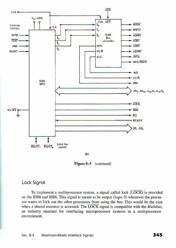
To implement a multiprocessor system, a signal called lock (LOCK) is providedon the 8088 and 8086. This signal is meant to be output (logic 0) whenever the ploces-sor wants io lock ont the other processon from using the bus. This would be the casewhen a shared resource is accessed. The LOCK signal is compatible with the Mrltibrr,an industry standard for interfacing microprocessor systems in a multiprocessor
Lock Signal
sec 8.4 Maximum-lvlode lnterface Srgnals 345

la
-'l.
o-id
iFiI
iit-iE
fiic
a
i6ta
6i-4
n
tbt
Figure 8-6 (.) Blocl diagrM of the 82E8. lReprjited tith permisjon oflnLel Corporation, E 1919) (b) Pin layout. (Rcprhted wnh pemission of htclCorporation. O i979)
Oueue Status Signals
Two orher signals produced by the 8088 and 8086. in the naxinum-mode microcomputer sysrem, are queue status outputs QSo and QSr thar fon ^2bjt queue status.,1e, QSlQSo. This code tells lhe extemal circuitry whal type of information wasrcmoved tiom the inltruction quene during the previous clock cycle. Figure 8 8 showsthe four dillerent queue siatus codes. Note thar QSlQSo = 0l indicates that the first byteof an insfirctioD was taken off the queue. As shown. the feich of the Dext byte of lheinstmclion is identilied by the code il. Whenevef the queue is resel due to a t|,tnsfer ofcontrol, |he reiniiialization codc 10 is ouiput.
CPU Cycle E2!6Comm.nrls2 s1 s0
0000
I
1
01010
01
Inlerupt Acknowledge
Hal l
-----to--o s9-
M_RDClvlFDC
frfrJa A-Mwc
Figure 8-7 Bus staius codes. (Repnnbd wnh permisior of l.rel CoiPoratiotr. O 1979)
t46 The 8088 and 8086 Mjcroprocessors Chap I

Local Bus Control Signals
In a maximum mode configuration, the minimum-mode HOLD and HLDA inter-face of the 8088/8086 is also changed. These two signals arc rcplaced by requen/qruntl,r€r RQ/CTo and RQ/GTj. They provide a prioritized bus access mechanism for access-ing the local bus.
8.5 ELECTRICAL CHAMCTERISTICS
ln the preceding sections, the pin layout and minimum- and maxinum-mode interfacesignals of the 8088 and 8086 microprocessors were intoduced. Herc we will firsl look atthe power supply ratings of these processors and then their input and output electricelcharacteristics.
Looking at Fig. 8 l(a), we find that power is applied between pin 40 (V".) and pinsI(GND) and 20(GND). Pins I and 20 should be connected together. The nominal valueof V.. is specified as +5 V dc with a tolerance of =10Eo This ineans that the 8088 or8086 will operate conectly as long as the ditrerence in voltage between V"" and GND isgreater than 4-5 V dc and less than 5.5 V dc. At room temperature (25oC), both tbe 8088and 8086 draw a maximum of 340 mA from the supply.
Let us now look at the dc yO characteristics of ihe microprocessor-that is. itsinput and output logic levels. These ratings tell the minimun and ma{imum vollages torthe 0 and I logic states for which the circuit witl opente corectly Different values arespecilied for the inputs atd outputs.
Figure 8-9 shows the I/O voliage specifications for the 8088 Notice thal the min-imum logic I (highlevel) voltage ai an ouQut (VoH) js 2.4V This voltage is specilied fora test condition thai identifies the arnount of current being sourced by the ou@ut (IoJ as-,100 pA. Al1 processors must be tesled during manufacturing to ensure that under thslest condition the vollages at all outputs will remain above the value of VoH-i"
os1 osn OuaueSlrlur
0 No Operalion. Ourin! lhsclock cycl€, nolhing was
0 Firsl Syle. The bylstakan lrom lheqleue wss the lirsl byle ol the
1 ( h i g h ) 0 Ou€ue Emply. The queue hasbe€n reini l is l i red as a rssultol lhesreculion ol a transfer inslruction.
l Subssqusnl Byte. The byte lakenIrom ths queue was a subsequ€nlbyle ol the inslrucllon.
figure 8-8 Queue status codes.(Reprinted lith pernisslon of lntelCorporanon, O 1979)
sec.8.5 ElectricalCharacteristics 347

+2.0 v
+2,4 V
v.. + 0.5 v
Figure 8-9 I/O voltage levels.
lnput voltage levels are specified in a similar way; except here the rarings identifythe range of voltage that will be correctly identified as a logic 0 or a logic 1 a1 an input.For inslance, voltages in the range Vn
",i. = -0.5 V to VL,,"* = +0.8 V represent a vilid
logic 0 (lower level) dt an input ofthe 8088.The I/O voltage levels of the 8086 microprocessor are identicai to ihose for ihe
8088 as shown in Fig. 8-9. However, therc is one difference in the iest conditions. For the8086, VoL is measued at 2.5 mA instead of 2,0 mA,
A 8,6 SYSTEM CLOCK
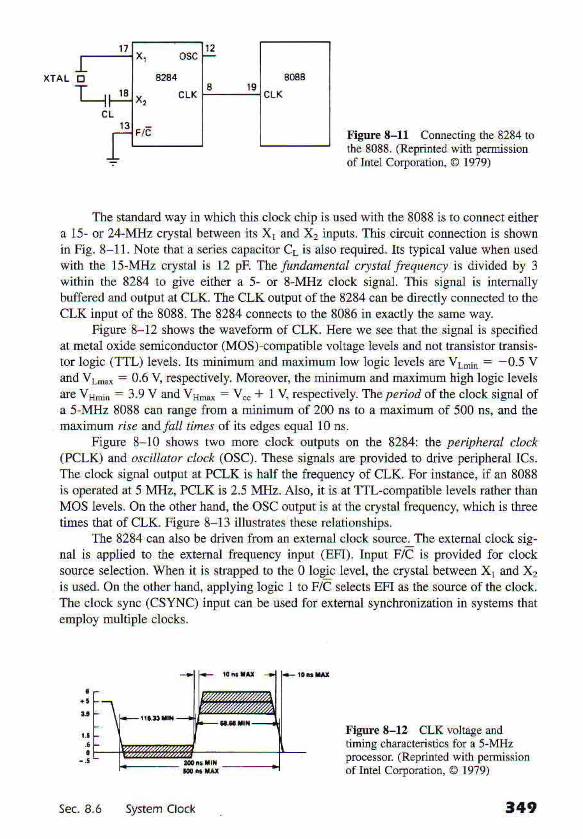
The dme base for synchronization of the internal and extemal operations of the micro-pro.essor in a microcompuier system is provided by the cl.rc* (CLK) input signal, At pfe-sent, the 8088 is available in two different speeds. Tbe standard pan op€rutes ot 5 MHz andthe 8088-2 operales at 8 MHz. On the olber hand, the 8086 microprocessor is manufactuledin three sp€edsr the s-MHz 8086, the 8-MHz 8086-2, and dle lo-MHz 8086-1. The 8284clock generator and driver IC generate$ CLK, Figul€ 8-I0 is a block diagram ofthis device.
Iigu.e 8-10 Block diagam of the 8284 clock generator (Repnnted wilh peFmisslon of Intel Corporation. @ 1979)
348 The 8088 and 8086 Microorocessors chao- 8
- CLK
Ftd
The standard way in which this clock chip is used with the 8088 is to connect eithera 15- or 24-MHz crystal between its Xr and X2 inputs. This circuir connecrion is shownin Fig. 8 11. Note that a series capacitor CL is also required. trs lpical value when usedwith the 15-MHz crystal is 12 pF The funnanental crystal frcquerry is divided by 3within tbe 8284 to give either a 5- or 8-MHz clock signal. This signal is internallybuffered and output at CLK. The CLK output of the 8284 can be dnectly connected to theCLK input of the 8088. The 8284 connects to the 8086 in exacdy the same way.
Figure 8-12 shows the wavefom of CLK. Here we see that the signal is specifiedat metal onde semiconductor O4os)-compatible voltage levels and noi transistor transis-ior logic (TTL) levels. Its minimu.n and maximun low logic levels a.e VLdi : -0.5 Vand Vlda = 0.6 Y respectively. Moreover the minimum and marimum high logic levelsare Vs-i" = 3.9 V and VHms : Ve + 1 Y respectively. The petrd of the clo€k signal ofa 5 MHz 8088 can range froln a nininum of 200 ns to a mrximum of 500 ns, and themaxilj.u.m rise and fatl tines of its edges equal 10 ns.
Figure 8-10 shows two morc clock outputs on the 8284i tte peripheml cLock(PCLK) and oscilLdtor clo.* (OSC). These signals are provided to drive peripherai ICs.The clock signal output at PCLK is half the frequency of CLK. For instance, if an 8088is operated at 5 MHz, PCLK is 2.5 MHz. Also, it is at TTl-compatible levels rather thanMOS levels. On dre other hand, the OSC output is at the crystal frequency, which is thre€times that of CLK. Figure 8-13 illustrates these relationships.
T]le 8284 can also be driven from an extemal clock sourcejhe extemal clock sig-nal is applied to ihe exiemal frequency input (EFI). Input F/C is provided for clocksource selection. Wlen it is strapped to the 0 Iogic level, the crystal between Xr and X,is used. On the other hand. applyins logic I to F/C selects EFI as the source of the clock.The clock sync (CSYNC) input can be used for extemal synchronization in systems thatemploy multiple clocks.
IigN E-ll Conneting the 8284 lothe 8088. (Reprinted with penissionof lntei Cor?oration. @ 1979)
Figue E-12 CLK voltage andtiming chdacteristics for a 5-MHzprocessor (Reprinted wilh permissjonof Intel Corpontion, O 1979)
s e c . 8 - 6 System Clock 341)

Figure 8-13 Relationshjp belween CLK and PCLK. (Reprinted with pennis-sion of lntel Coryonrlon, O I 979)
EMMPLE 8,4
If the CLK input ofan 8086 MPU is to be ddven by 4 9-MHz signat, wha! speed versionof the 8086 must be used and what frequency crystal must be attnched to the 8284?
SolutionThe 8086-l is the version of the 8086 that can be run at 9 MHz. To create rhe 9-MHzclock, a 27-MHz crystal must b€ used on the 8284,
A 8,7 BUS CYCLE AND TIME STATES
A Dlli c)cb defines th€ basic opemlion that a microproces$or pertbrms to communicatewith external devices, Examples of bus cycles are the memory lead, Demoly write,input/output read, and inpuvoutput write. As shown in Fig. 8-14(a), a bus cycle co e-sponds to a sequence of events that stall with an address being output on the system bosfollowed by a read or write data transfer During these operations, the MpU produces aseries of control sigrals to conlrol rhe direction and tinring of the bus.
The bus cycle of the 8088 and 8086 microprocessors consists of at least four clockp€riods. These four time states are called T , T2, Tj, rnd Td. During Tr, the MpU puB anaddrcss on the bus, For a write memory cycle, data are put on the bus during state T, andmaintained through T3 and Ta. When a read cycle is ro be pedomed, the b s is first purin the high-Z state during T, and then ihe data to be read musr be available on the busdudng T1 and Ta. These foLrr clock staLes gi\e a bus .jlle duration of 125 ns X 4 =500 ns in an 8-MHz 8088 system.
If no bus cycles are reqxired, the microFocessor perforns whal are knowr as td?rrat€r. During these states, no bus activiry takes place. Each idle staG is one clock periodlong, and any number ol them can be inserred berween bus cyctes. Figure 8-14(b) showstwo bus cycles separated by idle states. Idle stares are perfomed if the insrruction queuein. ide lhe nicroproce*, ' r i . tL l l dnd ir aoe. nor neea,o 'e, ,d or wrire operrnd. from
Wait noks .al also be inseded into a bus c),cle. This is done in response ro arequest by an event in extemal hardware instead of an internal evenr such as a full queue.
350 The 8088 rnd 8086 MrLroproce\o.\ Chdp. 8

-"-r"t"t"-]*"--l*-ru
tl--___________x__]@-".". "*,*....- JL J _""r","."".
J 1-;';y;,".pgi** *'
FisuE E-r4 (a) Bus cycle ctock periods. (Reprinkn wirh lemisior of InlelCorporation, O 1979) (b) Bus cycle with idle states. (Retrtured with pemis-siotr of Iltel Corporaliorr O 1979) (c) Bus cycle with wait states. (Reprintedwirh pemi$ion of Intel CorpoEtion, O 19?9)
ln fact, the READY input of the MPU is Fovided spe.ificaly for rhis pupose. Figwe8 14(c) shows that logic 0 at this input indicates thar tlle cuneni bus cycle should not becompleted. As long as READY is held at the 0 leve], wait states are inserred berweenstates T3 and Ta of the curent bus cycle, and the dara rhar were or the bus during T3 aremaintained. The bus cycle is not completed until rhe extemal hardware returns READYback to the 1 logic level. This extends the duration of the bus cycle, thereby permitringthe use of slower memory and I/O devices in the system.
EMMPLE 8.5
What is the duration of the bus cycle in the 8088-based microcomputer if the clock is8 MIIZ and two wait states are iDserted?
Solution
The duration of the bus cycle in an s-MHz system is give, in general by
t y . = 5 0 0 n s + N x 1 2 5 n s
Bus Cycle and llme States5ec. 8.7 35t

In this expression N stands for the number of wait states. For a bus cycle wirh two wair
t y" = 500rs + 2 x 125 ns = 500 ns + 250ns= 750 ns
8.8 HARDWARE ORGANIZATION OF THE MEMORYADDRESS SPACE
From a hardware point of view. the memory address spaces of the 8088 and 8086-basedmicrocomputers are organized ditrerently. Figure 8-i5(a) shows rhat the 8088's memorysubsystem is irnplemented as a single 1M X 8 memory bank. Looking ar &e block diagram in Fig. 8-15(a), we see that these byte-wide storage locations are assigned lo con-secutive addresses over the range from 0000016 through FFFFFT6. During rnemory oper-ations, a 20,bit ad&ess is applied to the memory bank over address lines Ao ttuough A,,It is this adahess that selecrs the storage location thar is to be a.cessed. Bltes of data aretrdnsferred beiween ihe 8088 and memory over data bus lines Do through D7.
On the other hand, the 8086's lMbyte memory address space, as shown in Fis.8 l5(b), is implenented as rwo independenr 512Kbyte banks: the torr (et)en) bank and6e high (odd) bank Data. bltes associated with an even address (0000016, 0000216. etc.)reside in the low bant, and those with odd addresses (0000116, 0000316, etc.) reside in rhehish bank.
512t lYtEs t12r( srrEs
!i
(b)
Fisur€ 8-15 (a) lM x 8 hemory bank of rhe 8088. (b) Hish and lowmemory banks of tle 8086. (Reprinted wirh permision of Intel Corporation,o 1979)
.]IM SYTES
2
0
352 The 4088 and 8086 Microorocessors ChaD. 8

The diagram in Fig. 8 l5(b) shows that for the 8086 ad&ess bits, A1 through Are
select the storage location that is to be accessed. They are applied to both banks in paral-
lel. A0 and bank high enable (BHE) are used as bank-select signals. lngic 0 at A$ idenn-
fies an even-addressed byte of data and causes the low bant of memory to be enabled. On
the othgi hand, BHE equal to 0 enables the high bank to access an odd'adahessed byte of
data. Each of the memory banl6 provides half of the 8086's 16-bi! data bus. Notic€ that
the lower bank transfers bytes of data over data lines Do through D7, while data transfers
for a high bant( use Ds through D,5.We iust saw that the memory subsystem of the 8088-based micrccomputer system
is actually organized as 8_bit bytes, not as 16-bit words However' the contents of any two
consecutive byte storage tocations can be accessed as a word The lower-addressed b)4e
is the least significant byte of the word. and the higher-addressed byte is its most signifi-
capt byte- I€t us now look at how a b)4e and a wod of data are read from memory.Figure 8-16(a) shows how a byte-memory operation is perfomEd to the storage
Iocation at addrcss X. As shown in the diagram, the adahess is supplied lo the memory
(b1
Hardwarc Organjzation
Figue E-16 (a) B}'te trdsfer bY the8088. (b) word tmsfer by the 8088
( x + 1 t
Sec- 8.8 of the MemoryAddress Space 35
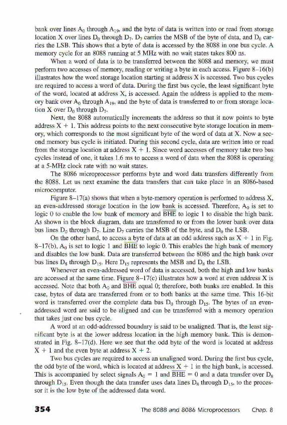
bank over lines A0 through Are, and the byre of data is wrilten into or read from storagelocarion X orer l ine. Do-hrough D-. D cdJr ies rhe \4SB o, rhe oyteot dara.dnd D0c;-ries the LSB. This shows thar a byte of data is accessed by rhe 8088 jn one bus cvcle. Amemory cJ(le lor an F088 rLrnning ar 5 MH,, w t- no $aiL .rare. rate. 800 n..
When a word of data is ro be transfer"ed berween rhe 8088 and mernorv. we mustDerform rso acce$e. ofremor). readjog or sriling a bytF in eacn acce-. Figure 8 r6lblillustates how the word storage locarion starting al address X is accessed. Two bus cyclesare requred ro access a word of data. During the fusr bus cycle, the least significanr byteof the word, located at address X. is accessed. Again the address is applied ro the memoD banx over A. lhrough Aro. and .he b)re ot data i . Fan.fered to o, i roln uo"g. 'o.u.tron X over Do tbrough D?.
Next, the 8088 automatically increments rhe address so rhat it now points to bvtedddre$ X + L hi . addre$ poin.. lo lhe ne\r con.ecut ive b)re. lorage tocal ion in menory, which conesponds ro the most significant byte of the word of dara at X. Now a sec-ond memory bus cycle is initiated. Durirg rhis second cycte, dara are writren inro or readl?om the storage location at address X + 1. Since word accesses of memory take two buscycles instead of one, it takes 1.6 ms to access a word of data when the 80S8 is oDerarinsdr r 5 MH,, cloc,( rale w h ao wail !!ares.
The 8086 .nicroprocessor performs byte and word data transfe$ differently fromthe 8088. Lel us next examine the dara transfers thar can take place in an 8086-based
Fignre 8 17(a) shows that when a byte-memory operarion is pedorhed ro address X,an even-addrcssed storage locarion in dle low bank is accessed. Therefbre. A" is sei ro.ogic 0 ro enJble rhe lo$ bant of nemoD drd BHE- lo togrc I ru di.abre rne hrsh bao*.45 \hou n ia rhe block diJgran. d d are nan.rened ro or rrom rhe toser bdnl ;\ er ddrdbus lines D0 tbrough D?. Line D? carries rhe MSB of the byte, and Do rhe LSB.
On the other hand. to access a byte of data at an odd address such as X + I in Fig.8 l7,br. q0 r" .el lo log,c I and BHF ro logic 0. Thi. enable, rne high banx of memor)and disables the low bank. Daia are transfered between rhe 8086 dnd the hish bant overDu, r ine( Ds dTough D.. He? Dr, repre.enrr rhe MSB and DR rhe LSB.
Whenever an even,addressed word of data is accessed, both the high and tow banksare accessed at the same time. Figure 8-17(c) iltusrraies how a word ar even address X isaccessed. Nole that both A0 and BHE equat 0; therefore, both bants are enabled. In rhiscase, bytes of data are ransfefed from or to borh banks at rhe same rime. This l6_bitword is aansfeffed over the comp]ete data bus Do through Dr5. The byres of an even_addressed word are said io be aligned and can be rransfened with a memorv oDeration_nd lale\ ,rst one bus cycte.
A word at an odd-addressed boundary is said to be unaligned. That is, the least sig_nificanl byte is at the lower address location in rhe high memory bank. This is demon-strated in Fig. 8 17(d). Here we see that the odd byte of the word is locaied ar ad&essX + I and the even byre at address X + 2.
Two bus cycles are required to access an unaligned word. Dwing the first bus cycle,the odd byte of ihe word, which is locared ar addrcss X + 1 in the hish bank. is accessed.Pr ' . h rccompan'eJ b) \etecr . ignaloAo- t and BtU - 0 and a Jara ran,rer over D"through Dr5. Even though rhe data transfer uses data tines Ds through Dr5, to the proces",or ;_ i . the low b\te of lhe dddre,,ed oard $uro
354 The 8088 dna 8086 V.(rop.o.es\or5 Chap. 8
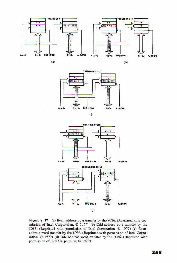
( d )
Figue 8-17 (a) Even-address byte transfd by the 8086. (Reprlnred with pernision of Intei Corporariotr, O 1979) (b) Odd'addres byte tmsfer by ihe8086. (Reprinted with permision of Inte] Corloetion. O 1979) (c) Evenaddres word transfer by the 8086. (Reprinted with permision of Iniel Corlo-ration, O i979) (d) Odd addres wod iransfer by ihe 8086. (Reprhted wilhpemission of Int€l Cor?oration. O 1979)
355

Next, the 8086 auromarically increments the address so thar A. = 0. This reDresenrslhe nerl addreq, in memory uhich ,s eren. Then a \econd memon bu. c\cte L iniridred.During rhi , ,econd clcle. rhe e\en b)re localed ar X - 2 in rhe to\ banl is acces,ed.The data transfer takes place over,bus lines D0 through D7. Tbis tansfer is accomDanie.db)& 0and BHE - l . lo rhe proce.soj. dr i , ie rhehigh blreofrheuord ol daia.
EMMPLE 8.6
Is the word at memory address 0123116 of an 8086 based microcompurer atigned or misaligned? How many bus cycles are required to read it ftom memory?
SolutionThe first byte of the word is rhe second byre ar the aligned-word address 0123016. There_fore, the word is misaligned and requires two bus cycles to be read from memory
8.9 ADDRESS BUS STATUS CODES
Whenever a memory bus cycle is in plogress, an address bus status code S,S. is outDutb) r l 'e prccessor The 5rdru, code rs n utr ipte\ed wirh aodre.. birs Ar- and qr". ' f t r . ruo.bit code is outpur aa the same rime the dara are caded ov€r the dara lines.
Bits Sr and 53 together fom a 2,bir binary code thar idenrilies which one of the foursegment regrters was used to generate rhe physical address thar was oumur duinq iheaddresr period in rhe currenr bur c)cle. The tow add,"ss but snru,,oae, are lisrea inFig. 8-4. Here we find thar code SaSr = 00 idenrifies the exrra segmenr register 01 ide.rtifies the stack segment register, l0 identifies the code sesment regisret and 11 identifiesthe data segrnent regisrer
These status codes are ourput in both the minimum and rhe maximum modes. Thecodes can be examined by external circuifty. For example, they can be decoded withextemal circuirry ro enable separate tMbyte adatress spaces fbr ES, SS, CS, and DS. Inthis way, the menory address reach of the microprocessor can be expanded to 4Mbytes.
8.I O MEMORY CONTROL SIGNATS
Earlier in the chaprer we saw rhat similar control signats are produced in rhe maximumand minimum mode. Moreover, we found ihat in rhe ninimum mode, the 8088 and 8086microprocesson produce all the conrrot signals. But in the maximum mode, the g288 buscontoller produces them. Here we wiil look morc closely ar each of these sisnais andrbeir tunctjons u irh re,pecr lo memory inlerface operdrion.
Minimum-Mode Memory Control Signals
In the 8088 rnicrocompurer sysrern shown in Fig. 8_18, which is configureal forLhe minimum mode otoperar ion. $e t ind lhar the connot srgnat( pror jded ro.upDon rheinrerface ro rhe memory \ub\ysrem are ALL, tOA4, Dt/R, RLi. WR. arl nf|,r. T|*"
356 The 80aa and 8086 Microprocessors Chap. I

8@8
Io/i
DEN
sso
Figure 8-18 Mininun-no.le 8088 remory hterface.
control signals are required to tefl the memory subsysiem when the bus is carrying a va]idaddress, in which dircction data arc to be tansfen€d over the bus, when valid write dataare on the bus, and when to pur read data on the bus.Fot example, ad.dress latch enable(ALE) signals extemal circuit y that a valid address is on the bus. It is a pnlse to the Ilogic level alrd is used to latch the address in extemal circuitry.
T\e input-ouput/memory AO/ll{) and d^ta tnnsmit/rece e (DT/R) lines signalextemal circuitry whether a menory or I/O bus cycle is itr progress and whether the 8088will transmit or receive data over the bus- Dudng all memory bus cycles, IO/M is held atthe 0 logic level. The 8088 switches DT/R to Iogic I during the data transfer part of thebus cycle, the bus is in the transmit mode, and data are written into memory On the oaherhand, it sets DT,.R to logic 0 to signal that the bus is in the rcceive mode, which corle-sponds to reading of memiry.
The signars r"d/ (RD) and lrn& (WR) identit that a read or write bus cycle,respectively, is in progess. The 8088 switches WR to logic 0 to signal memory that awrite cycle is taking place over the bus. On the other hand, RD is svritched to logic 0whenever a read cycle is in progess. During a[ memory operations, the 8088 producesone other control signal, ddta enable @El0.l.og:,c O at &is outPut is used to enable thedata bus.
Slrtus l;n" SSO is also part ofthe minimum-mode memory interface. The logic leveltbat is output on this line during Iead bus cycles identfies whether a code or data access isin progress. SSO is set to logic 0 whenever instmction code is read from memory
The contol signals for the 8086's midmum-node memory interface differ in threeways. First, the 8088's IO/M signal is replaced by the m€mory/input-output (M/IO) sig-nal. Whenever a memory bus cycle is in plogress, ihe M/IO output is switched to logic 1.Second, the si$al SSO is removed fiom the interface. Thftd. a new signal, ,anft tlgllenable (BHE), has been added to the interface. BHE is used as a select input for the highbant of memory in the 8086's memory subsystem- That is, logic 0 is output on this line
Sec. LI0 Memory Control Signals 357

during the ad&ess part of all rhe bus cycles in which dara i, the hish-bank Darr of memory is to be accessed.
Maximum-Mode Memory Control Signals
W}len the 8088 is conligured to work in rhe maximum mode. it does nor diectlvpro\ide all rl.e control .ignal( ro suppon rhe memor) inrerface. Incread. an exremal bu'controllet the 8288, provides memory conmands and contol signats. Figure 8 19 showsan 8088 connected in this wav
Specificalt). rhe WR. tOA4. DT,R. bLN. ALE. and SSO rignat rine. on rhe 8088are Lhanget. The) dre replaced virh nultiproce\\ot /or* rlOCKr signat. a b,l \rdrar!94e (SrS1SJ, and a 4rar? rrarrr cod? (QSreS0). The 8088 stitl does produce rbe sisnalRD. which provides lhe.ame lJncl ion as i l d id in minimum mode
The 3-bil bus status code qS,Sn is nutput prior to the iritiation of eacb bus cycle.It identjfies which lype ofbus cycle is to follow This code is input to the g2gg bus con_troller Here it is decoded to identify which type of bus cycle command signals must begeneraled,
Figure 8-20 shows the relationship belween the bus status codes and the types ofbus cycles produced, Also shown in this chart are the names of the co$esDondins com-mand signals rhar are generaed ar the ourputs of the 8288. For instance, rhe inprir codeS:SrSo equal to 100 fldicares rhat an inerruction ferch bus cycle is ro take place. Since fieinsruction ferch is a memory read. lhe 8288 makes the nenory read connand (fr-RDC1output switch to logic 0.
Anorher bus command provrded tbr the memory subsystem is SrSl56 equal ro I J0.This represents a memory write cycle and it causes both the memory write conmand
Figure E-19 Mdimun-mod€ 8088 menory interface.
8288
358 The 8088 and 8086 MicroprocessorsChap. 8
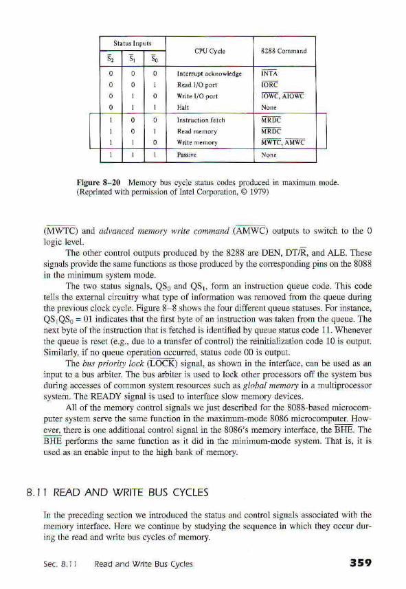
Figure 8-20 Memory bus cycle stalus codes p.oduc€d in ffiimum mode.(Reprinted with pemission of lntel Corporation, @ 1979)
(MWTC) and advanced menary \rfte command (|\NN{C) outputs to slvitch to the 0logic le\e' .
The other control oulputs produced by the 8288 arc DEN, DT,/R. and AlE Thesesignals provide the sane tunctions as those prcduced by dle conesponding pins on the 8088
in the minimun system mode.The two status signals. QSo and QSr, lorm an instruction queue code This code
tells the exlernal circuitry what type of infomation was removed from the queue duringthe previous clock cycle. Figure 8-8 sholvs the four diffetent queue statuses- For instance'
QSTQSo = Ol indicates that the lirst byte of an instruction was ta.ken from the qneue Thenext byte of the instruction that is letched is identified by queue status code 1 l Whenever
the queue is reset (e.g., due to a transfer of control) the reinitialization code 10 is outputSimitarly, il no queue operatio occurred, status code 00 is outpur.
The bus prioriD lock (LOCK) signal, as shown in the inteface, can be used as aninput to a bus arbiter. The bus arbiier is used to lock other processoff off the system busduring accesses of conmon sysGm resources such as glordl nendD' in a muldprocessorsystem. The READY signal is used to intedace slow memory devlces.
A11 of the memory control si$als we just described for lhe 8088'based microcom-puter system serve the same function in the maximum-mode 8086 microcomputer How
ever there is one additional contol signal in the 8086's memory inlerface, the BHE. The
BHE performs the same function as it did in fie ninimum-mode svstem That is, it is
used as an enable input to the high ban& of memory'
8.I1 READ AND WRITE BUS CYCLES
In the precediry section we introduced lhe slatus and contml signals associated with tl'e
memory interface. Here we continue by studying the sequence in which thev occur dur-ing the read and write bus cycles of memory
s! sr
0 I
0I
iflrAtoRcrovc-, A-i6Fa
I
MRDCMIDcMwlt. AMwc
sec. 8.1I Read and write Bus cycles 35t
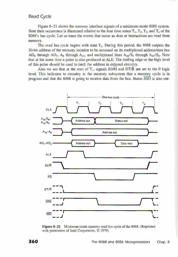
Read Cycle
Figure 8-21 shows the memory interface signals of a minimum-mode 8088 system.Here their occurence is illustrared relarive ro the four time stares Tr, Tz, Tr. and T1 of the8088's bus cycle. Let us trace ihe events that occur as data or instructions are read from
The rcad bus q,cle begtns with srate Tr. During this period, the 8088 ourputs rhe20'bit address of fie memory location to be accessed on its mulriplexed address/data busADo through AD?, As through Ar, and multiplexed lines A6/51 tbrough Arr/56. Norethat al the same time a pulse is also produced at ALE. The rrailing edge or the high levelof this pulse should be used to latch the addrcss in extemll circuitry.
Al.o \^e cee lhal ar he {a1 ofT.. s iCnal, lO/\4 l ld DT,R are,et to rhe 0logiclevel. This indicares to circuitry in rhe memory subsystem ihar a memory cycle is inp,! ,sre\\ ana rha, ,he 8088 ; lornr ro recei\e d d from ,be bu.. Srdru. SSO r. at .o our-
IO/M
RO
DT/F- - - t
figure E-21 Minimum,mode memory read bus rycte of the 8088. (Reprintedwith lemision of intel Corporation, O I 979)
360 The 8088 and 8086 MicroDrocessors Chao. I

Dut at this time. Noie thai all tkee of these signals are maintained at these logic levels
ihroughout all four periods of the bus cycle.Beginning with stale T2, status bits 53 through 56 are outPut on the upper foul
ad{tress bus lines A16 through Arr. Rernember that bits 53 and S1 identifv to extemal cir-
cuitry which segrnent register was used to generate the address just output. This status
information is maintained ttuough periods T3 and T+ The part of the ad&ess output on
address bus lines As tlrough Ars is naintained tfuough states Tr. Tr, and T4. On the other
hand. address/data bus lines ADo through AD? are put in the high-Z state du.ing Tr'
Lare in penod T. RD i . 'q i lched ro logic 0 Ttu' indjcarec ro $e memoD srbsls-re.rl |ndr r rerd clc,e r' in progess DE\ I' ssirched ro'ogic 0 'o enable erkmal circuirr)
to allow the data lo move from memory onto the midoprocessor's daia bus.As shown in the lvaveforms, input data are read by the 8088 during T3. The mem-
ory must provide valid data during T3 and maintain it until after the processor terminates
the rcad operation. As Fig. 8-21 shows, ir is in T! that the 8088 switches RD to the inac-
tive I logic level to lerninate the read operation. DEN retums to its inactive logic level
late during Ta to disable the exiernal circuitry, which aliows data to move from memory
ro the processor. The read cycle is now complete.A timing diagram for the 8086's memory read cvcle is Siven in Fig 8-22(a) Com-
paring these waveforms to lhose of the 8088 in Fig. 8-21' we ind just four differencesi
BHE- is output along with lhe address dudng Tr; the data rcad bv the 8086 during T3 can
be carried over a[ 16 data bus lines; M,4O. which replaces IOA4, is switched to logic I
Fisur€ s-22 (a) Minimum-mode memory read bus cvcle of dre 8086'
I R;or in ed +trn pemi. . ion o l lnre lCorporal io O loTq' 'b ' \4drmum_modemr:^ry ead bu, cycle of .he d08{-., Repr Inred wirl. Derris,ion ol lnrel CoFporalior O 1979)
Sec. 8.1 I Read and Write Bus Cycles 361
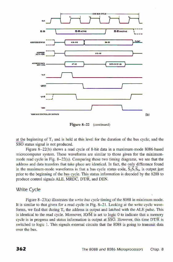
FigureS-22 (continued)
at the beginning ofTr and is held at this level for the duration of the bus cycle; and theSSO status signal is not produced.
Fignre 8-22(b) shows a read cycle of s-bit data in a Ina\ilnum mode 8086 basedmicrocomputer system. These wavefoms are similar ro those given for the minimun-mode read cycle in Fig. 8 22(a). Comparing these two timing diagrams, we see that theaddress and data tnnsfers that take place are identical. In fact, the only difference lbundin the maximum mode waveforms is that a bus cycle slatus coite, SrSrS0, is output jFsrprior to the beginning of the bus cycle. This status information is decoded by the 8288 toproduce control signals ALE, MRDC. DT/R, and DEN.
V/rite Cycle
Figure 8-23(a) illustrates rhe tnite bus clcie trmingof the 8088 in ninimummode.It is similar to that given for a rcad cycle in Fig. 8-21. Lookjng at the write cycle wave-forms. we find that dudng Tr the address is output and latched witb the ALE pulse. Thisis identical to lhe read cycle. Moreover, IO/l'{ is set to logic 0 to indicate that a memorycycle is in progress and status information is ouiput at SSO. However. this time DT,&. isswitched to logic L This signals extemal circuits that lhe 8088 is going to tansmit data
362 The 8088 and 8086 Microprocessors Chap. I

ro/ti
w3
ora __j
DEN
sso
L .
_ -J--1 r-
r , (a)
Figure E-23 (a) MitriDDm mode mmory wite b6 cycle of the 8088.(Repiinled with p€mission of Intel Corporatior @ 1979) (b) Mdimum-nodememory wrile bus cycle of the 8086. (Reprinted with penission of Intel CoFporation, @ 1979)
As T, starts, the 8088 switches WR to logic 0. This tells the memory subsystem thata write operation is to follow over the bus. The 8088 puts the data on the bus late in T,and maintains the data valid though Ta. The writing of data into memory starts as WRbecomes 0, and continues as it charyes to I early'in Ta. DEN enables the extemal cir-cuitry to provide a path for data ftom the processor to the memory. This completes the
Just as we described for the read bus cycle, the write cycle of the 8086 ditrers fromthat of the 8088 in four ways; agaia SSO is not prcduced! Bm isiutput along with theaddressi data ,re canied over a 16 data bl]s lines: and fnally, M/IO is the complementof dle 8088's IO/M signal. The wavefoms in Fig. 8-23(b) ilustrate a wrjte cycle of worddata in a ma,\imum-mode 8086 system.
sec. 8.1 I Read and Write Bus Cycles 363

FiguE E-23 (co lnued)
^' 8.i2 MEMORY INTERFACE CIRCUITS
This section describes the memory interface circuits of an 8086-based microcomputersystem. The 8086 system was selected instead of an 8088 microcomputer because it ismore complex. Figue 8-24 shows a menory interface diagram for a ma,\imum-mode8086-based microcomputer syslem. Here we find that the interface includes the 8288 buscontoller, address bus latches and an address decoder. data bus transceiver/buffers. andbank read and w.jte control logic. The 8088 microcompuGr is simpler in that the inter-face does not rcquire bank wdte control logic because its address space is organized as asinele banl.
Looking at Fig. 8 24, we see that bus shrus code signals Sz, Sr, and So, which arcoutputs of the 8086, are supplied direcdy to the 8288 bus controller. Here ftey aredecoded to produce the command and conhol signals needed to coordinate data transfersover the bus. Figure 8-2o]ighlights the slalus codes that reiate to the memory interface.For example, the code S2S]S0 : 101 indicates thai a data memory read bus cycle is inprogress. This code makes rhe MRDC conmand output of the bus control logic slvitch tologic 0. Note in Fig. 8-24 that MRDC is applied to the banh read control logic.
Next let us look at how the address bus is latched, buffered, and decoded. Lookingat Fig. 8-24, we see that address lines Ao through AD are latched along with contlol sig-nal Bm in the ad&ess bus latch. The latched addrcss lines AjrL tlrough ArrL are
t64 The 8088 and 8086 Microprocessors chap. 8
-cE" cE-,
wR,
WR.
Fd
BHE
Figure 8-Z Memory interface block diagram.
decoded lo produce chip enable outpub Cq Lhrough eE . Notice $ar lhe 8288 bus con-troller produces the address latch enable (ALE) control signal from SrSlSo. ALE isapplied to lhe CLK input of the lalches ad strobes the bits of the address and bank high€nable signal into the ad&ess bus latches. The address latch devices buffer these signals.Latched address lines ArL tbmugh Ar6L and Cq tuough CE7 are applied directly to thememory subsystem.
Du.ing read bus cycles, the MRDC ouqut of the bus control logic enables ihe bytesof data at the outputs of the memory subsystem onto data bus lines Do tbrough D15. Dur-ing read operations from memory fte batrk read control logic determines whether thedata are read Iiom one of the two memory banks or ftom bolh. This depends on whethera byt€- or word-data transfer is taling place over fte bus.
Similarly during wrile brts cycles. rhe IvfwTC ourpur of he bu. coDtrol logicerables byt€s of data from the data bus Do drough DE to be written into the memory. Thebank wnte conaol logic determtues to which memory bank the da(a are wdtten-
5ec. 8.12 Memory lnteriace Cjrcuits t6 t
Note in Fig. 8 24 that in ihe baDl write control logic the latched bad( high enable
{g4LBmL and address l;ne AoL are galed wilh lhe memory $rile conmand signa]MWTC toTroduce 4 leparale wrile enable signal for each bank. These signals aredenoted as WRL' and WRL. For dample, if a word of dala is Io be wriLlcn |o memory overdata bus lines D0 tbrougl Drr, both WRu and WRL-are switched to their acrive 0 logiclevel. Similarly the memory read control logic uses MRDC, AoL. and BIIEL to gene teRDu and RDL sisnals for bank read control.
The bus transceiven conirol the direction of dala ransfer between the MPU mdmemory subsysten In Fig. 8 24, we see that the opoation of the t ansceiver is controlled by the DT/R and DEN ouFuts of thc buJi controllcr DEN is applied to the ENinput of the transceiverj dnd enables then fo. operatioD. This happens during all read andwriie bus cycles. DT/R selects the direction of data transfer ttuough the devices. Note thatit is supplied ro lhe DIR input of lhe dala bus ransceiYels- W})en a read cycle is inprogress. DT/R is \et to 0 and dala are passed from thc memory subsystem 10 the MPU.On dre other hand. when a write cycle is taking place. DT/R is switched to logic I anddata are carried from the MPU to the memory subsyslem.
Address Bus tatches and Buffers
The 7,lFl73 is xn examplc of an octal latch dcvicc that can be used to implementthe ddr.€rr /d.., section of the 8086 s memor) i erface circuit. A block diagram of thisdevice is shown m Fig. 8-25(a) and fts intemal circuit] is shown in Fig. 8-25(b). Notethat ii accepF eight inpuis: lD through SD. As long as the clock (C) inpnt is ar logic I,the outpxts of fte D-t-vpe ltip-flops follow fte logic level of the data applied to their corresponding inputs. When C is swilched ro logic 0, fte current contenls of tbe D type fiipflops de latched. The laiched inrbmation in the flip flopr is not output at data outputs 1Qthrough 8Q unless the output'control (OC) irpu. of the buffers that fo ow dre larches isat logic 0.IfOC is at logic l, fte outpuls are in ihe high-impedance srare- Figure 8 25(c)summdizes this operation.
In the 8086 microcomputer system, the 20 address lines (ADo AD 5, A 6 Ar,)and the bank higlr enable signal BHE a.e nomally la.ched ;n ihe address bus latch. Thecircuit configuration shown in Fig. 8 26 can be used to latch these signals. Fixing OCat the 0 logic le\€l permanendy enables lalched outputs AoL rhrough AreL and BHEL.Moreover. thc address information is latched at the outputs as the ALE signal ffom thebus controller returns to losic 0 that is, when the CLK itrput of all devices is switchedio logic 0.
In general. it is importail to m;nimize the propagation delay ofihe address signalsas they go through the bus in erface circuit. The switching propeny of the 7,1F373 latchesthat deternine this delay for.he cncuit of Fig. 8 26 is called enableao-output propaga-tion d?ldJ and has a maxirnum value of 13 ns. By selecting fasi latches that is, iatcheswith a shoner Fopagation delay time a maximum amount of the 8086's bus cycle tirneis preserved for fte access timc of the memory deviccs. In this way slower. lower costmemory ICs can be used. These latches also provide bulTering for the 8086 s addresslines. The outpuis of the latch can sint a maxnnum of 2,1 lnA.
356 lhe 80aa and 4086 Microorocesso6 Chao I

0c
c
1 D
i D
m
o
ao
-
1 0
20
30
Ito
m
80
Figure 8-25 (a) Block diaSm of d @ta] D'rype latch. (b) Circuit diagm of the74F373. (CouJtesy of Texas lnstruments Incorporated) (c) Operation of the 74F373.(Courtesy of Texas Instrum€nts hcorpoFted).
O-C Enabl€ C D o
L I.] H
L H L L
z

Figurc 8-26 Address latch cjrcuit.
Bank V/rite and Bank Read Control Logic
The memory of the 8086 nicrocomputer is organized in upper and lower banks. Ilrequires sepdrate wrire dnd read control signais for the rwo banks. The logic circuit inFig. 8 27 shows how the bank wdte contlol signals. wRu lbr the upper bank and wR!for the lower bank can be generaied from lhe bus controller signals WRTC, the addressbus larch signals AoL and BmL. Two OR gates are used for this purpose.
Similar io the bank wdte conirol logic circuit. the bant rcad contol logic circuiican be designed to generale RDu. the read for the upper bank of memory. and RDb theread for the lower bank. Figure 8 28 illustrates such a circuit. Note that ihe circuit usesthe MRDC signal from the bus controller
Data Bus Transceivers
'lhe dala bus h lnsceiNer block of the bus intertace circuir cm be implemented with74F245 octal bus transceiver ICs- Figure 8 29(a) shows a block diagram of this device.Nole that i1s bidirectional input/ourput Iines are caued Aj through As and B I drough Bs.Looking at the circuit diagram in Fig. 8 29(b). we see dut the G input is used to enable
oct-Tv' ' l l l
|] ltlIr*I r---L
f"'v
iLl
t
- [
oaAHE
t6a The 8088 and 8086 Microprocessors Chap. I
1432
Figurc 8-27 Ba'k wite control logic.
the buffer for op€ration. On the other h'ind, the logic level at the direction (DIIR) inputselects the direction in which data are transfen€d through the device. For instarrce, logic0 at this input sets the transceiver to pass data {iom the B lines to the A lines. Si witchingDIR to logic I reverses the direction of data tlansfer.
Figure 8-30 shows a circuit that implements the data bus transceiver bl,ock of thebus interface circuit using the 74F245. For the 16-bit data bus of the 8086 micr(rcomputer,two devices are required. Here the DIR input is ddven by the signal data transr"ioit/receive(DT/R), and G is supptied by data bus effable (DEN). These signals aie outlputs of the8288 bus conholler
Another key function of the data bus hansceiver circuit is to buffer t.loe &ta buslines. This capability is defined by how much current the devices can sint at rheir outputs.Ihe IoL rating of the 74F245 is 64 mA.
MRDC
BHEL
Figure E-2E Banl read control logi..
Memory Interface Circuits
7432
5e.. a. l2 36t

Addft 3ss Decoders
Figure 8-29 (a) Block diaeram ofthe 74F245 0cl2l bidirecrional bustmsceiver (b) Circuir diagram of tle74F245. (Coudesy of Texas lnstro-
A s shown in Fig. 8-31, the adnrcss decoder n Ae 8086 micrdcomput€r system islocated at the output side of the addrcss latch. A typicat device used to pelfolm thisde.ode 1 :unction is fte 74F139 dual2line to 4line decoder Figures 8 32(a) and (b) showa block diagrarn and circuit diagram for tbis device, respectively. When the enable (G)input is r at its actrve 0 logic level, the output conesponding to the code at the BA inputs
t70 The 8088 and 8086 Micfoprocessors Chap. 8

:N
i R
Mic,op@s$d d.ta b6 ] I
G
DBo-D8,
G
74F245
Figure 8-31 Address bus connguation with ad.liess decoding.
Sec. 8.12 Memory Inteface Circuits
Figm 8J0 Data bus transceiver circuit.
switches.o the 0logic level. For instance, when BA : 01, output Yr is logic 0. The tablein Fig. 8-32(c) summarizes the operation of the 74F139.
The circuit in Fig. 8 33 employs the addrcss decoder configuration shown in Fig.8 31. Note that address Lines ArTL and ArsL are applied to the A and B inputs of the/,1flJq decoder. fte address line Aror i( used ro erable one ol rbe decoders and {r,r.obtained using an inverter, enables the second decoder ol the 74F139. Each decoder gen-erates four chip enable (CE) outruts. Thus both decoders of the 74F139 together Foducethe eight outputs CEo ttuough CE7.
M crop'@e$r dddr* bus
371

Y2
Y3
e,* I'^
L2B
Ftgure 8-32 (a) Block diasrm of th€ 74F139 2line to 4line decoder/denu|iplexer (b) circuit diagrm of the 74F139. (Counesy of Texas Inslru-nents Incoryorated) (c) oleration of the 74F139 de.oder. (counesy of TexasInstruments Inco@rated)
372
c&
cEr
cE3
cE4
cE5
cE€
CF,
Figur€ 8-33 Add.ress de.oder circuit.
The block diagram of another cornmonly used d€coder, the 74F138, is shown inFig. 8-34(a). The 74F138 is similar to the 74F139, except that it is a single three-Iine toeight-line decoder The circuit used in this device is shown in Fig. 8-34(b). Note that itcan be used to produce eight CE ouQuts. The table in Fig. 8-34(c) descdbes the operation of the 74F138. Here we find that when enabled, only the output that coresponds tothe code at rhe CBA inputs swirches to the active 0 logic level.
The circuit in Fig.8 35 uses the 74F138 to generate chip enable signals CEo tbroughCE7 by decoding address lines Ar7L. ArsL, andArrL. Connecting the enable inputs to +5Vand ground permanently enables the decoder. The advantage of using the 74F138 over the74F139 for decoding is that it does not re4uire an extra inverto to genemte eight chipenable sisnals.
cEr
1Y374F139
. 2Y0
2v1
2\2
2\3
sec. 8.12 Memory lnterface Ckcuits 313
YO
\2
Y3
Y5
Y6
Y7
(c)
Frsure 8-34 - d' qb.k dT.cr-al,- ol-:T::: lf .ff"iJ,i'"T'iii "ifll,T
tc;unes\ of Te\as Ins!ruments rcorp"rar'"' ''' '
(Counesy ofTe\as ln\mments licorPonre! |
dzAGzE
'*t*'

c1
c2B
cBz
cE3
cE4
cEj
@1
Figure E-35 Addres decoder circuitusing 74Fi38.
B. i3 PROGRAMMABLE LOGIC ARMYS
In the last section we found that brsic logic devices such as latches, tiansceivers. anddecoders are rcquired in the bus interface section of the 8086 microcomputer system. Weshowed that these functions werc performed with standard logic devices such as the 74F373octal imnspareni laich,74F245 ocral bus tansceiver and 74F139 two-tne ro four-linedecodet respectively. Today prcgrunnable logic aftay (PLA) devices are becoming veryimpotant ir the desigr of microcomputer systems. For example, address and control signaldecoding in the memory interface in Fig. 8-24 can be inplemenled with PLAS. instead ofwith sepaEte logic ICs. Unlike the earlier mentioned devices, PLAS do not implement aspecific logic function. Instead, rlEy arc general-purpose logic devic€s dlat have fie abiliryto perfonn a wide variety of specialized loglc tunctions. A PLA contains a general-purposeAN'D OR NOT aray of logic gate circuits. The user has the ability to interconnect theinputs to the AND gates of this array. The defnition of these inputs determines the logicfunction that is implemented. The process used to connect or disconnect inputs of lhe ANDgate anay is known as prosldnm,n& which leads to the name programmable logic array.
PLA5. GAt"s. and EPLD5
A variety of different types of PLA devices lre available- Early devices were atlmanufactured with the bipolar semiconductor process, These devices are referred to asPALi aDd renain iD use today. Bipolar devices arc programmed with an interconnect paltem by burning out fuse links widin the device. ln the initial state, all of these tuse linksare intact. During pmgramming. unwanted linls are open-circuited by injecting a current
sec 8.13 Programmable Logic Arrays 375

tlmugh the fuse to bum it out. For this reason, once a device is programned it cannot
be reused. If a design rnodificaiion is required in the pattem, a new device must beprograrnrned and substituted for the original device. Since PALS are made with an older
bipolar technology, they lre limited to sinpler funcrions and characrerized by slower
operating speeds and hiSh power consumption.Newer PLA devices are manufactured with the CMOS process. With this Focess'
very complex, high-speed, low-power devices can be made. Two kinds of CMOS PLAS
are in wiale use today; the GA, and the tPrD. These devices differ in the type of CMOS
technology used in their design. GALS are designed ns:j..g ekcti&ll, erasable ftttd'onlv
r1?r,orl (E':ROM) technology. The inpuroutput operation of this device is determinedby rhe p.ogranming of cells. These etectrically progrannnable cells are also electricallv
efasable. For this reason, a GAL can be used for one apPlication' erased, and then re-
programmed for another application. EPLDS are similar io GALS in that thev can beprogrammedr eraseal, and reused; however, the erase mechanism is different. They are
manufactured with electricallr prcSrannable read onb memory (EPROM) technologvThat is, they employ EPROM cells inst€ad of E'zROM cells. Therefore, to be erased an
EPLD must be exposed to ultraviolet lighi. GALS and EPLDS are cunently the mosa
rapidly growing segments of the PLA marketplace.
Block Diagram of a PLA
The block diagram h Fig. 8 36 rcprcsents a typical PLA Looking at this diagram,
we see thal it has 16 input leads, marked Io through IL5 There are eight output leads'
labeled F0 lhrough F7. This PLA is equipped with ttue€-state outputs For this reason. ii
has a chip-enable conaol lead. In the block diagram. fiis control input is narked CE. The
logic level of CE determines if the outputs are enabled or disabled.When a PLA is used to implement random logic firnctions. the inPuts represent
Boolean variables, and the outputs are used to provide eight separate random logic func_
tions. The intemal AND OR-NOT army is programmed to define a sum-of-product equa-
tion for each of lhese outputs in tems of the inputs and their complemenls ln this way,
Figure E-36 Block diacIm of aPLA. (Reprlited wilh the permissionof Walter A. Tri€bel)
The 8088 and a086 Microprocessors chap. 8376

we see that the logic levels applied at inputs I0 tbrough Ir5 and the Progaaming of theAND array determine what logic levels are produced at outpul't Fo tbrough F7. Therefore,the capacity of a PLA is measwed by thee Fopertiesr the number of inputs, the numberof outputs, and the number of product terms (P-tems).
Architecture of a PtA
We just pointed out that the circuitry of a PLA is a general purPose AND-OR-NOIaray. Figue 8 3?(a) shows this architecture. Herc we see that the input buffen supplyinput signals A and B and their complemenis A and B. Programmable connections in theAND aray permit any combination of these inputs to b€ combined to form a productterm. The Foduct term outputs of the AND array are supPlied to fixed inputs of the
t -*".,1*tII
F=AB+AB
44E l!:_ 37 G) Basic PLA archilectue. (b) Inllenenting the losic tunction F =
(AB + AB).
sec. a.l3 Programmable Logjc Afays 317

OR array. The output of the OR gate produces a sum-of-products futction. Finally, the
The circuit in Fig. 8 37(b) shows how dre function F - (AB + AB) is implementedwidl the AND OR NOT aray. Notice that an X marked into the AND array means that th€fuse is left intact, and no marking means !ba! it has been blown to folm an open circuii. Rrihis reason. the upper AND gate is connected to A and B and Foduces the product termAB. The second AND gate from the top connects to A and B to produce the Foduct termAB. The bottom AND gaG is marked with an X to indicate fiar it is not in use. Cates likethis that arc not to be active should have aI of their input tuse Links left inlact.
Figurc 8 38(a) shows the circuit structure that is most $ridely used in PLAS. Itdiffers from the circuit shown in Fig. 8-37(a) in two wals. First, the inverter has a pro-grammable thre€-state control and can be used to isolate the logic function Aom the oul_put. Second, the bnffered output is fed back to fbnn anolher set of inputs to the ANDarray. This new output conligumlion permits the output pin to be progJallllrcd to wo* as^ standard autput, standad input, or logic-cantrcllzd inputlor,tput For instance, if theupper AND gate. which is the control gate fbr the output buffer is set up to permanendyenable the inverter and the fuse links for ils inputs that arc fed back from lhe outputs areall blown open, the output functions as a standard output.
Kt-
rnler tef complements th is fundjon.
INPUT
OIJTPUT
(b) FEEOSACK
rigu.e 8-38 (a) Tylical PLA archltecture. (Counesy of Teaas lnslrunents Incorpo-Eted) (b) PLA *nb output larch. (courlesy of Texas I.strunent$ Incorporated)
CLOCK
374 lhe 8088 dnd 8086 Vr.'op.ocessoA Chcp. 8
PLAS are also available in {'hich the ou9uts are Iatched with registers Figure
8-38(b) shows a circuit for this rype of device. Here we see that the ouFut of $e OR gate
is applied to the D input of a clocked D t)?e flip-flop In this wav' the logic level produced
by the AND OR array is not presented at the ouiput until a pulse is first applied at the
CLOCK input. Futherrnore, the feedback input is Foduced ftom the complement€d outpui of ihe flip-flop, not the output ofthe inverter This configuration is known as a PL4 unn
re|istered outputs atrd is designed to sirnpliry implenentation of state ,?4.*r,e designs'
Standard PALru Devices
Now that we bave introduced the rypes of PLAS, block diagram of tlle PLA' and
internal drchitecture of the PLA, let us continue by examini4 a few of the widely used
PAL devices. A PAl, or a programmable anay logic, is a PLA in which the OR arav is
fixed; only the AND array is programmableThe 16L8 is a widely used PAL IC. lts intemal circui.rv and pin numbering are
shown in Fig. 8-39(a). This device is housed h a 2Gpin package' as shown in Fig
8-39(b). Looking at this diagam. we see rhat it employs the PLA drchitectue illustrated
in Fig. 8-38(a). Note that it has 10 dedicated input pins. All of.hese pins are labeled I'
There are also two dedicated outputs, which are labeled with the letter O' and six prograrnmable I/O lines, which are labeled yO Using fte programmable I/O lines' rhe num
ber of input lines can be expanded to as many as 16 inputs or the Nmber of outputs can
be increased to a5 many as eigh. lines-All the 16L8's inpuLs are buffered and produce both the original form of the signal
and its complement. The outputs of the butrer are applied to the inputs of the AND arrav'
This array is capable of producing 64 product terms- Noie that the AND gates are
arranged into eight groups of eiglt. The outputs of seven gates in each of these goups areused as inputs 1o an OR gate, and the eighth ouFut is used to p.oduce an enable signal
for the corresponding tlEee-state output buffer' In this way. we see thd rhe 16L8 is capa-
ble of producing up to seven Foduct terms for each ourpu! and the Foduct ierms can be
formed using any coqbination of lie 16 inputsThe l6L8 is manufactured with bipolar t€chnology- It operates {iom a +5V :l:109'
dc power supply and draws a maximum of 180 aA. Moreover, all it! inpuis and outputsare at TTL compatible voltage le\€ls. This device exhibits high-speed inpui-output prop-
agation delays. In fact, the maximum l-to-O Fopagation delay is rated as 7 nsAnother widely used PAL is the 20L8 devic€. l-ooking at the circuitv of this device
in Fig. 8-40(a), we see that it is similar to that of the 16L8 jusr described Howeve! the
20L8 has a maxim m of 20 inputs, eight outpuls, and 64 P terms. The device's 24-pinpackase is sllown in Fig. 8 40(b)
The 16R8 is also a popular 20 pin PLA. The circuit diagram al}d pin lavout for this
device ;re shown in Figs. 8-41(a) and O), rcspectively. FIom Fig. 8 41(a), we find that
its eight fixed I inpurs and AND-OR array are essedially the same as those of the 1 6L8'There iii oDe chnge. The outputs of eight AND gates. instead of seven, are supplied to
the inputs of each OR gare.A number of changes have been made at the ouiput side of the 16R8- Note thai the
outputs of the OR gates are fiIst latched h D type flip-flops wirh the CLK signal Thev
are then buffered and supplied to the eight Q outputs- Another charge is tbat the enable
Sec. 8.l3 Programmable Logic Affays 37t

tE vo
tll] "o
!l 'o
rigure 8-39 {a) l6L8 circuit diaSrd. (Counesy of Texar lnslruments Incor?orated)(b) 16L8 pin layout. (Couliesy ofTexas Ilstrumenis Incorporated)
380
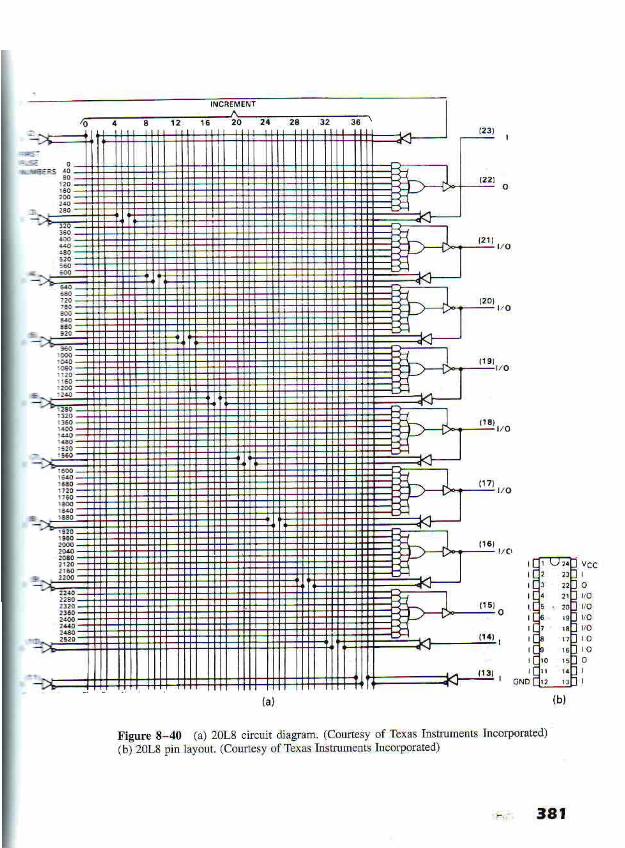
Figure 8-40 (a) 20L8 ctcuit diagram. (Courtesy of Texas Instruments Incorporated)(b) 20L8 lin layout. (Courtesy of Texas hstrumenls lncorporaled)
3A l

Figure 8-41 (a) 16R8 cncuir dia81am. (Couresy of Texas Instrutnerts lncorporated)(b) 16R8 pin layout. (Couresy of Texas Instrunents lncorporated)
6,:':
342

srgnals for the ootput inverters ale no longer prognmmable. Now the logic level of theOE control input enables a[ three-state outputs
The last change is in the part of the circuit that Foduces the feedback inpuis ln the16R8, these eight inpu! signals are derived ftom ihe complementary output of the colle-
sponding larch instead of the output of the buffer' Fo. this rcasoq the ouq)ut leads can nolonger be pro$ainmed to work as direct inputs.
The 20R8 is the register output venior of the 20L8 PAl Its circuit dia$am and pin
layout are give! in Figs. 8 42(a) atrd (b). respectively
Expanding PtA CaPacity
Sone appiications have requimments that exceed the capacity of a single PLA IC- For
instance, a 16L8 device has the abiliry to supply a rnaximum of 16 inputs' 8 outputs. and
64 product terms. ConDecting several devices t€erher can expand capacity Lei us now look
a! the way in which PLAS are intercomected to expand $e number ol inputs and outputs.ff a single PLA does not have enough outputs, two or more devices can be con-
nected togelher into the configuration of Fig. 8 43(a) Here vr'e see that the inputs I0
through Ir5 on the two devices are individualy connected in parallel This connectiondoes not change the number of inputs.
On the olher hand, the eight outputs of the two PLAS are separately used to formthe upper and lower btaes of a 16-bit output word. The bits of this wod are denoted as
Oo through Or5. So with this conneciion, we have doubled the number of outputs.\vhetr data are applied to the inputs, PLA I outputs ihe eight leart significant bits
of data. At the same instant PLA 2 outputs the eight most significant bits These outputscan be used to represent individual logic tunctions.
Another limitation on the apPlication of PLAS is the number of inplrts- The ma,\rmum number of inputs on a single 16L8 is 16. Howevet additional lcs can be connecled
to expand the capacity of inputs Figue 8-43(b) shows how one additional input is addedThis permits a 17-bit input denored as Io through 116 The new bit 116 is supplied tbroughinverters to the CE inputs on the two PLAS. At the output side of the PLAS, outputs Oothrough 07 of the two devices are individually connected in paralel. To inplemenl thiscoMeclion. PLA detrce' $i!h open-colle{lor or three-\tale ourpulc musl be rsed
When 116 is logic 0, CE on PLA 1 is logic 0. This embles the device for operation'and the oulput functions coded for input I0 tfuough Ir5 are output at Oo tbrough 07- At thesame instant, CE on PLA 2 is iogic 1 and it rernains disabled Making the logic level of
116 equal to 1 disables Pl-A 1 aDd enables PLA 2 Now ihe input at Io through Ir5 causesthe output function defined by PLA 2 to be output at Oo through 07 Actually, this con-nection doubles the number of Foduct terms as well as increases the number of inputs
8,I4 TYPES OF INPUT/OUTPUT
The input/output system of the microprocessor allows peripherals to provide data orreceive results of processing tbe data. This is done using I/O ports The 8088 and 8086
microcomputers can employ two diffemnt types of input/output (I/O): isolakd I/O at].d
menory-mapped I/O. These l/O methods diffe. in how I/O pofts are mapped into the
8088/8086's address spaces. Some microcomputer systems employ both kinds of I/O-
sec 8.14 Types of Input/Output 383

6---i--i----1t-- t;3{
(a) {b)
Figure 8-,12 (a) 20R8 circuit diaelam. (Couiresy of Texas Instruments Incorporated)(b) 20R8 pin lalour. (Courtesy of Te{as Insrtunents Incorporated)
344

llL..-i_
II
(a)
:
Figure 8-43 (a) ExPanding outPut word length. (Reprified wirh tbe penis;sid of Warler A. Tnebel) (b) Exlanding in?ut woid len$l. (Reprirted withthe permission of Walier A. Triebel)
that is, some peripheral lcs are treated as isolaied I/O devices and oihers as memory-
rnapped I/O devices. Let us now look at each of these ryPes of I/O.
lsolated Input,/OutPut
Wlten using isolated I/O in a microcomputer system, the I/O devices are treated
separate from memory. This is achieved because the so{iwarc and hardwaxe architectures
oithe 8088/8086 support sepamte memory and I/O address spaces. Figure 8-zg illus-
trates these memory and I/O address spaces.In our study of 8088/8086 software architectue in Chapter 2, we exarnined these
address spaces from a software point of view. We found that infbrnation in memory or at
sec. Li4 Types of lnput/Output 345

Figure 8-44 8088/8086 nemory and
I/O pofs is organized as bytes of data; that lhe memory address space contains lM con-
,".uilu" Uyt" iaa..ttes io the range 0000016 through FFFFFL6I and that the I/O address
.o,. . .oniuin ' O+K.on..cuLi\e blre add'e'se. In Ine ran8e 0000r ' tuough FFFF "
Figure 8 45,ar iho\\s a more derailel] map of rhi' l/O add'e'c sp:ce Herc $e find
that the;ltes of data in rwo consecutive I/O addrcsses could be accessed as word-wide
data. For instance, l/O addresses 000016,000116' 000216, and 000316 can be treated as
independenr byte-wide l/O ports. ports 0. 1, 2, and 3, or pons 0 and 1 mav be considered
together as word-wide Pot 0.Note that the pan of the I/O ad&ess space in Fig 8-45(a) from address 000016
nhrough 00FFr6 is refered to as pdg€ a Cedain UO inslructions can only perform oper-
ations'to pots in this part ofrhe address rarge Olher I/O instruciions can input or output
data for pons anywhere in the I/O address spaceThis isolated merhod of I/O offers some advantages First, the complete lMbyte
memory address space is available for use urith memory' Second' special instuctions
have been provided in *re instruction set ol the 8088/8086 to perforn isolated I/o inp'rt
and ouD; operations. These instruciions have been tailored to maximize I/O pedor-
mance. i dis;dvantage of this rype of I/O is that all input and output data transfers musl
take piace betueen the AL or AX register and dre UO port
Memory-MapPed lnPut/OutPut
I/O devices can be placed in the memory address space of the microcomputer as
well as in the independent I/O address space. In this cdse, lhe MPU looks at the UO pon
as though it is a storage location in memory. For this reason' the method is known as
netnory napped I/O.ln a microcomputer system with menory-mapped I/O' some of the memory address
space is dedicated to l/O ports For example' in Fig. 8 45(b) the 4096 memory addresses m
tire range from E0000r6 throltgh E0FFFL'j are assigned to I/O devices Here the contents
of a<trtrlss E0000r6 represent b)'te-wide l/O port 0, and the conlents of addresses E0000t6
and 8000116 correspond to word-wide por 0
346 The aoaa and 8086 Microprocesso6 Chap S
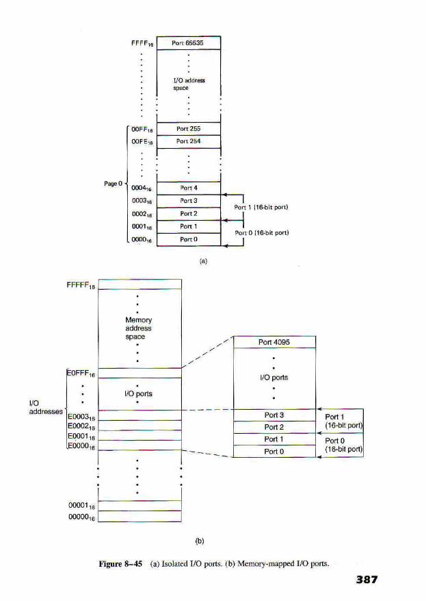
:
:
va :
E0oo316E0004sEoool ls
0000i6
(b)
risur€ 8-4s (a) Isolaied I/o ports. (b) Menory-napped I/o ports
(16-bilpod
(15-bil po't)
347
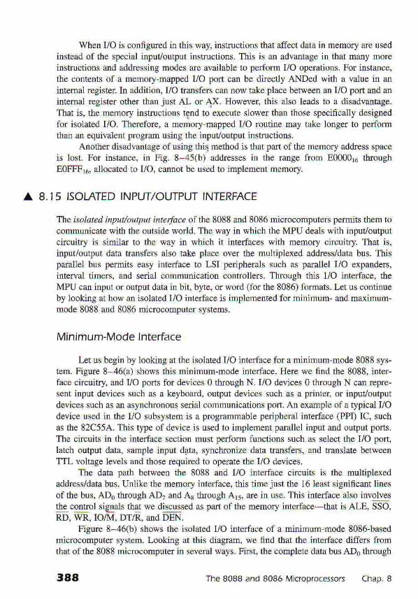
Wllen I/O is configured in this way, inslructions that affect data in memory are usedinstead of ihe special input/output inslructions This is an advantage in that many moreinstructions and addrcssjng modes are available io perform I/O operations For instance'
the contents of a memory-mapped l/O poll can be directly ANDed with a value in an
intemal register. In addition, l/O tansfers can now take place between an l/O port and anin@mal register other than ju$ Af or A,I. However, lhis also leads to a disadvantage.That is, the memory instructions tgnd to exe.ute slower than those specifically desigrcdfor isolated UO. Therefore, a memory mapped I/O routine may take longer to perform
than an equivalent progrl]m using the inputoutput tnstructlons.Anolher disadvantage of using this method is drat part of the memo.y address space
is lost. For instance, in Fig. 8-45(b) addresses in the range from 8000016 ihroughE0FFFI6. allocated to I/O, cannot be used to jmplement memory
8.I 5 ISOLATED INPUT/OUTPUT INTERFACE
The isolated input/output t,?t€dac€ of the 8088 and 8086 microcomputers permits them to
communicate with the outside world. Tlre way in whicb the MPU deals with inpuvoutputcircuitry is similar to the way in which il interfaces with memory circuitry. That is'input/output data transfers also lake place over lhe multiplexed address/data bus. Thisparallel bus permits easy interface to LSI peripherals such as Parallel I/O expanders.interval timers. and serial cornmunication controllers. Through this UO interface, lheMPU can input or output data in bit, byte, or word (for ile 8086) formats Let us continueby looking at how an isolated UO interface is implemented for minirnum- and maxirnum-mode 8088 and 8086 microcomputer systems.
Minimum-Mode Interface
Let us begin by looking at the isolated I/O interface for a minimum-mode 8088 sys-
tem. Figure 8-46(a) shows this minimum-mode interface. Here we find the 8088' inter-face ciicuity, and VO poris for devices 0 tbrough N I/O devices 0 through N can repre-sent input devices such as a keybo.rd, output devices such as a printer' or inpuvoutpuidevices such as an asynchronous serial communications port An example of a rypical I/Odevice used in the l/O subsystem is a programmable peripheral interface (PPI) IC' such
as the 82C55A. This type of device is used to implement parallel input and output poris
The circuiis in the interface seclion must perform functions such as select the I/O port'
lalch output data. sample input dgta, synchronize data transfers, and translate betwe€nTIL voltage levels and ihose required to operate the I/O devices.
The data path between the 8088 and l/O interface circuiis is the multiple)Gdaddress/data bus. Unlike the memory interface, fiis time just dre 16 least significant linesof the bus, ADo tlrough AD? and As rhough Ar5, are in use This interface also involvesthe control si$als that we discussed as pad of the memory interface-that is ALE, SSO.
RD. WR. IO,M. DTA.. and DEN.Figure 8-46(b) shows the isolared I/O intedace of a minimum-mode 8086-based
micrccomputer system. Looking at this diagram. we find thai the interface differs fromtbat of the 8088 microcomputer in several ways. First, the compleie data bus ADo through
384 The 8088 and 8086 Microorocessors chap B
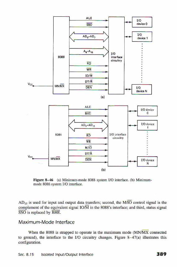
8@8
MN/MX
uo
vosso
, aDo-aD, )\---------------
Aa-A,a )----------------
FD
!o
IO/M
OEN uo
3036
MNA,IX
tHE
' ADo-ADr5 l\ - , / I
RD
VE
M/id
DT/F
tENN
(b)
risue 8-46 (a) Minimum-node 8088 syslem VO interface. (b) MinimDm-mode 8086 system I/O inlerface.
AD;. is u.ed for inpur and ourpur dararran'ter'r 'econd. rbe V,4O conrol .igal rs rhe
lg4llenent of the equivalent signal IOA4 in the 8088's interface; and third, status signalSSO is replaced by BHE.
Maximum-Mode lnterface
tvhen fie 8088 rs .trapped ro opemre rn rhe ma{mum mode r\4J\/M} corurecredto gound), rhe inteface to the I/O circuihy changes. Figure 8 47(a) illustrates thisconfigura.ion.
Sec. Ll5 lsolated lnput/Output Interface 349

vo
8233
3133
Figure 8-47 (a) Ma-\imum node 8088 systen I/O interface. (b) Mdlmummode 8086 systen I/O interface.
3to

s: 5,0 iNlA
I
rorvc. A-idwa
0
I
I
I
iliStMRDCfuwrc,AMw'c
Figure 8-4E l/O bus cycle slatus codes (Reprinled with pernision of IntelCorporalion, copyight/Intel cory. 1979)
As in the naximum-mode memory interface. lhe 8288 bus conholler produces lhe
control signals for the yO subsystem- The 8288 decodes bus command slatus codes out-put by the 8088 at S,SIS0. These codes tell which type of bus cvcle is in Fogless. If the
code coresponds to an I/O read bus cycle, the 8288 generates the /O rcad colllAlldl/tprr (IORC) and for an I/O write cycle it generacs l/O wite mnma n ouQuts GOWC)an,l (AIOWC). The 3288 also Foduces the control signals ALE, DT,&.' and DEN The
address and data transfer path between 8088 and ma\imum node UO intedace remains
address/data bus lin€s ADo through AD? and As through Ar iFigure 8-47(b) shows the maximum-mode isolated I/O intedace of an 8086 micro-
processor syslem. Therc are only two differences between this intedace diagram and thalfor the 8088 microprocessor As in the minimum mode, the tu1l 16-bit dara bus is the path
for data transfers, and lhe signal BHE, which is not supplied by the 8088' is included rn
the interface.The table in Fig. 8 48 shows the bus conmand status codes together with the com-
mand signals lhat they produce. Those for I/O bus cycles are highlighted The MPU indi-
cates that data are to be inpul (read I/O pori) by code S2SrS0 = 001- This code causes the
bus controller to produce control oulput I/O read command oORC) There is one otler code
that represents an ouQut bus cycle, the write UO polt code S,SrSo : 010. It produces two
output command srgnals: I/O \rrite cycle (IOWC) and advanced UO \lTite cycle (AIOWC)
These command sig:nals are used to enable data ftom the l/O ports onto the system bus dur-
rng al irpul operalion Jno from the MPU lo lhe l/O porl' during an ouFul operalion
8,I6 INPUT/OUTPUT DATA TRANSFERS
Input/output data transfers in the 8088 aid 8086 rnicrocomputers can be either byte-wide
or word-wide. The pon that is a(essed for input or outpui of daia is selected by an /o
drldr€rs. This address is specified as palt of the instruction thal performs the I/O operation'I/O addresses are 16 bits in length and are output by the 8088 to the l/O interface
over bus lines ADo through AD? and As tl oughAr5. ADo represents the LSB and Ar5 the
sec. Ll6 lnpuvoutput Data Transfers 3.rl
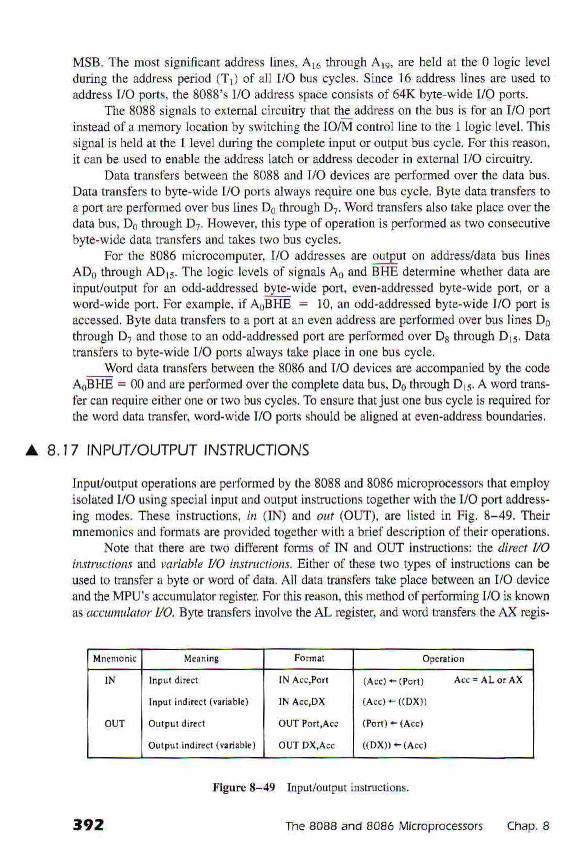
MSB. The most significant address lines, A16 through Arr, are held at the 0 logic lerel
during tlre sddress period (Tr) of all I/O bus cvcles Since 16 address lines are used to
address I/O oorts, the 8088's 1/O address space consists of 64K byte-wide I/O ports
The 8088 signals ro extemal circuitrv thai rhe address on the bus is for an I/O pon
inslead of a memory location bv switching the IO,M control line to the I logic level This
signal js held at the I level dxring the complete input or ouQut bus cvcle For th's reason'
it;an be used to enable the address latch or address decoder in external I/o circuit$'
Data transfers between the 8088 and I/O devices afe performed over the data bui'
Data tfttnslers to byte-wide I/O poris always require one bus cycle Byle data transten to
a pon dre performed over bus lines Do through D? Word transfeN also take place over the
data bus,16 througl17. However, this ivpe ofoperation is pedormed as two consecuiive
byte-wide data trinsfers and lakes two bus cycles.For the 8086 microcomputer, I/O a{ldresses ale output on iddress/data bus lines
ADo lhrough ADrr' The logic levels of signals A0 and BHE delermine whether data are
inpuVoutput for an odd-addressed byte-wide pon, even-addressed byte"wide-pttt' or a
word-wi;e port For example, if A0BHE = l0' an odd-addrcssed byte-wide I/O pon is
accessed, Byle data transfers to a pol,t ai an even address are perfbrmed over bus lines D0
through D?;nd lhose io an odd_addtessed pon are performed over Ds lhrcugh D 5 Data
lrAnsfers to byte-wide I/O pons always take place in one bus cycleword dala tmnsLers between lhe 8086 and I/O devices arc socompanied by lhe code
A0BE = 00 and are perfoDred over the complete data bur' Do through D 5 A word irans'
fer can requhe either one ol two bus cycles, To ensure that just one bus cycle is requircd for
the word data trmsfer, word'wlde I/O pofis should b€ aligned al even-address bouudaries
A 8, I7 INPUT/OUTPUT INSTRUCTIONS
Input/outpul operations ale pefbr med by the 8088 and 8086 micrcprocessols that employ
isolated llO using speclal input And oltput iDslructions logether wilh the I/O p-ort address-
i:rg motles. Thes=e instructions, ir (IN) and o&r (OUT), are lisied in Fig S-49' Tbeir
rnienonics and forrnats are provided together with a brjef description of their operations
Note tha! there arc two diilbrent forms of IN and OUT instructionsl the dircct 1/O
instluclio s and variahle I/O /tntt?rclr",{t. Either of these two rypes of instrxrclions can be
used 1() tansfer a byte or word of data. All dau anslers take Place between an I/O dev;ce
and the MPU'S accumulatof register For this reason, this nethod of perfoming l/O is known
^s arumulat.tr t/O Byte nansfers involve the AL rEgister, and nod transfeN the AX r€8is-
IN
o!rT
Output indn€ci (v.dable)
(A .O € lPor r ) Ac . = AL orAx
Fieure 8-49 Inputoutput nstructom
3q2 The 8088 and 8086 l\4icroprocessors chap. 8

ter. In fac! specjlying Al as the source or destination register in an I/O instuction indicates
that ii corresponds to a byte transfer. That is, b)te-wide or word-word input/output rs
setected by specifying the accumulator (Acc) in the instuction as AL or AX' respectivetv.ln a dire.t I/O instruction, the address of the I/O polt is specified as part of tbe
instruction. Eight bits are provided for this direct address. For this reason, its value is lim-
ited to the address range frorn 010 equals 00b to 25510 equals FFr6 This raage is referred
to as page 0 in the l/O address space.An example is the instruction
IN AI,, OFEH
As Fig. 8-49 shows, execution of this instrucaion causes ihe contents of ihe byte_wide I/Oporr at address FEr6 of the I/O address space to be input lo the AL register This datatransfer takes place in one input bus cycle
EMMPLE 8.7
Write a sequence of instroctions that will output the data FF16 to a byte'wide output port
at address AB L6 of dre I/O address space.
Solution
First, the AL register is loaded with FFr6 as an immediate operand in the instuction
MOV AL, OFFH
Now the data in AL can be ouFut to dle byte-wide outpLrt port with the instruction
OUT OABH, AL
The difference betwe€n the direct alrd variable l/O inslructions lies in the way in
which the address of the I/O port is specified. We jusi saw that for direct I/O instructions
an 8 bit addrcss is specified as part of the instruction. On the other hand. the variable I/O
instmctions use a 16 bit address thai resides in the DX register within the MPU The value
in DX is not an offset. It is the actual address that is to be output on ADo tfuough AD7 and
As through Ar5 during the I/O bus cycle. Since this address is a tulI 16 birs in length vari-
able I/O instuctions can access ports located anywhere in the 64K-byte VO address sPace.
When using eirher type of I/O instruction, the data musl be loaded into or rcmoved
from the AL or AX register before another input or output operaiion can be pefomled ln
the case of variable I/O instructions, the DX register must be toaded with (he addrcss
This requires execution of additional instructions. For instance, the instruction sequence
MOV DX, 0A00011IN AL, DXMOV B'-, AL
inputs the contents of lhe byte-wide input port at A000i6 of the I/O address space into AL
and then saves il in BL.
sec. 8.17 InPuVOutPut lnnftrcnons 3rt

EMMPLE 8.8
EXAMPLE 8,9
Data are to be read in from rwo blre-wide input polts at addrcsses AA16 and A916 andthen outpui as a word to a word-wide output port ar address B00016. Wrire a sequence ofinsiruciions to perfom this input/ourput operarion.
SolutionWe can firsr read in the byte from the pot at address AA16 inio AL and move it to AH.This is done fith the instructions
IN AL, OAAIIMOV AI{, Ni
Now the other byte, which is at port A96, can be read into AL by the instrucrion
IN AL, OA9H
The word is now held in AX. To wrile our the word of data, we load DX with rhe aaldress800016 and use a variable outpur insruction. This teads to rhe following:
MOV DX, OBOOOHouT Dx, ax
l. 8.IB INPUT/OUTPUT BUS CYCLES
In Section 8.15, we found that the isolated UO interface signats for the minimum mode8088 and 8086 miffocomputer sysrems are essentially rhe same as rhose invotved inthe memory interface. In fact. dle function, logic levels. and riming of a signals other
Write a s€ries of irsrructions that will output FFr6 ro an outpur port located at addressB00016 of the I/O address space.
SolutionThe DX register must firsr be loaded with the address of rhe ouFur port. This is done withthe instruction
M O V D X , 0 B 0 0 0 H
Next, the dara rhat are to be output must be loaded into AL with the insruction
MOV AL, OFFH
Finally. the data are outpui with the insrrucrion
OUT DX, AI-
3 t4 The 8088 dnd 8086 lvr'L.ooro.esrori Chap. 8
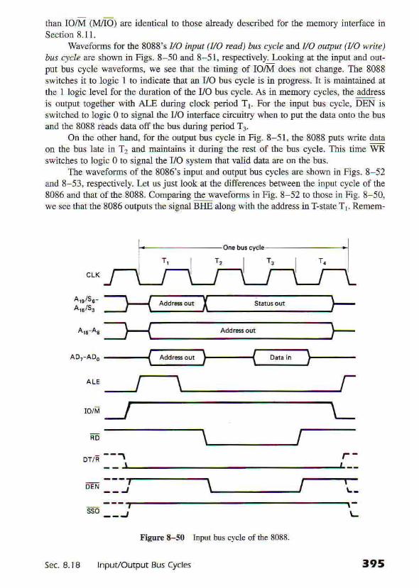
$an IO/M (M^O) are identical to those already described for the memory interface inSection 8.11.
Waveforms for the 8088's XO input (l/O rcad) bus ctcte and UO output (XO lt'rite),&r c],.lz are shown in Figs. 8 50 a 8-51, respectively. l,ookiry at the input and out-put bus cycle waveforms, we see that the timing of IO/M does not change. The 8088switches it to logic I to indicate that an I/O bus cycle is in progress. It is mai ained atthe I togic level for fte duration of ihe UO bus cycle. As in memory cycles, the adahessis output together with AIE dudng clock period Tr. For the jnput bus cycle, DEN isswitched to logi€ 0 to signal the UO ifierface cncuitry when to put the data onto the busand rhe 8088 reads data off the bus during period Tr.
On fte other hand, for the output bus cycle in Fig. 8-51, dre 8088 puts write dataon the bus late in T2 and maintains it during th€ rest of the bus cycle. This time WRswitches to logic 0 to signal the I/O system that lalid data are on the bus.
The waveforms of the 8086's inpul and output bus cycles are shown in Figs. 8-52and 8 53, rcspectively. Let us just look at the differences between the input cycle of the8086 and riat of the 8088. Conpariry the waveforms in Fig. 8-52 to those in Fig. 8 50,we see that the 8086 outputs the signal BHE along with the addrcss in T-state Tr. Remem-
I on. b$ cvil.
r ' l r ,
IO/M
F6
DT/F
$ o - - J
Fig@ 8-50 Inpd bns cycle of the 8088.
Inpuvoutput Bus Cycless e c . 8 . l 8 395

ro/fi
W U
DT/R-
DEN
---t
Figure 8-51 Outpul bus cycle olth€ 8088.
^',.iitrd:l@
Figurc 8-52 Input bus cycle ofthe 8086
Figure 8-53 OutPut bus cycle of the 8086
ber that for the 8086 microprocessor this signal is used aloDg with Ao to select rhe byte-wide or the word-wide porr. Next, lhe 8086's data lransfer path to the I/O intedace is the16-bit address/dafa bus, not 8 bjts as in the 8088 system. Thercfore. data transfels, whichrake place during T3, can take place over the lower 8 data bus lines, upper 8 data bus lines,or all 16 data bus lines. Thhd, dre 8086 outpuis logic 0 on the M/IO 1ine, while the 8088outputs logic 1 on the IO/M line. Thar is, the M,{O contol signal of the 8086 is the conplement of that of the 8088. Finally, the 8086 does rot produce an SSO output signal likethe one in the 8088.
REVIEW PROBLEMS
Section 8.l1. Name ihe tecbnology used to fabricale the 8088 and 8086 rnicroprocessors.
2. wlat is the transistor count of the 8088?
3. Wlich pin is used as the NMI input on the 8088?
4. which pin provides the BHE/S? outpnt signals on the 8086?
5. How much memory can dle 8088 and 8086 direcily address?
6. How large is ihe I/O address space of fie 8088 and 8086?
Section 8.27. How is minimurn or naximum mode of operation selected?
8. Describe ihe difference between the minimum-mode 8088 syst€m and ma,\imum_mode 8088 system.
tq7

9, What ouFut funciion is performed by pin 29 of dle 8088 when i" the minimummode? Maximum mode?
10. Is the sienal N4,/I'O an input or output of the 8086?11. Name one signal that is supplied by lhe 8088 but not by the 8086.12. Are the signals QSo and QSL produced in lhe minimum mode or maximum
Section 8.313. Wlar are rhe word lengths of the 8088\ addrcss bus and data bus? The 8086's
address bus and data bus?14. Does $e 8088 have a multiplexed address/dara bus or independent address and data
buses?15. What mnemonic is used to identify the least significani bit of the 8088's address
bus? The most significant bir of the 8088's data bus?16. \l/llat does status code SlSr : 01 mean in terms of lhe memory segment being
17. Which output is used to signal exiemal circuity fiat a byte of data is available onthe upper half of the 8086's data bus?
18, What does the logic level on M,{b signal to extemal circuitry in an 8086 micro,
19. Which output is used to signal external circuity in an 8088-based microcomputerlhat valid data is on the bus during a write cycle?
20. What signal does a nininun-mode 8088 respond with when it acknowledges anaciive inlerupt request?
21. Wlich sigr)als implement the DMA interface in a mininun-mode 8088 or 8086 lmicrocomputer system?
22. Lisi the signals of the 8088 that are put in the high-Z staie in response to a DMA
Section 8.423. ldentify the signal lines of tbe 8088 that are different for the minimum-mode and
ma,{imum mode interfaces.24. Whar siatus outputs of the 8088 are inputs to rhe 8288?25, Whar maximun'mode contol signals are generated by the 8288?26. What function does the LOCK signal serve in a ma{imum mode 8088 micro-
computer system?27. What status code is output by the 8088 to rhe 8288 if a memory read bus cycle is
taking place?28. What connand output becomes active if the status inpurs of the 828 8 are 1002?29. ff lhe 8088 executes a julnp instruction, what queue status code would be output?30. What signals are provide.d for local bus control in a ma{imum-mode 8088 system?
394 The 8088 and 8086 Micfoprocessors Chap. 8
Section 8.531. ffiat is the range of power suppty voltage over which rhe 8089 is guarant€ed to
work correcily?32. What is the maxinum value of volrage rhat is considered a valid togic 0 ar bit D0 of
the 8088's data bus? Assume rhat the oueut is sintdng 2 InA.33, What is the mininum value of voltage that would rcpresenr a vatid togic 1 at rhe
INTR input of rhe 8088?34. At what value curent is Volmd measured on the 8086?
Section 8.635. At v,hat speeds are 8088s generally avaitable?36. What frequency crystal must be connected berween ihe Xr and X? inputs of rhe
clock generator if an 8088-2 is ro run ai tul1 speed?37. What clock ourputs are produce.d by the 8284? Wlat would be their frequencies if
a 30-MHz crystal were used?38. What are the logic levels of the clock waveforms applied ro the 8088?
Section 8.739. How many ciock srares are in an 8088 bus cycte that has no wait states? How are
these states denoted?40. Wlat is the duration ofthe bus cycle for a 5 MHz 8088 that is running at tuI1 speed
and with no wait stares?41. What is an idle srate?42. Wlat is a wait stare?43. If an 8086 running at 10 MHz perfonns bus cycles with two wail states, whar is the
duration of the bus cycle?
Section 8.844. How is the memory of an 8088 microcompurer organized from a hardware poinr ot
view? An 8086 microcompurer?45, Give an overview of how a byte of data is read from memory addrcss B0003t6 of an
8088-based microcornpute! and list the memory control signals along with theiractive logic leveis that occur during the memory read bus cycle.
46. Give an overview of how a word of data is wriften to memory starting ai actdressA000016 of an 8088 based microcompute! ,nd tisi the memory conaol signatstogether with their acrive logic levels that occur dwing the mernory write cycle.
47. In which banl of memory in an 8086-based microconputer are odd-adatressed byresof data stored? Whar bank select signal is used to enable this bant of memory?
48. Over which of the 8086's dara bus lines are even addressed byres of dara transferredand which bank selecr signal is active?
49, List the memory control signals rogether with their active logic levels that occurwhen a word of data is writter io memory address A000016 in a minimum,mode8086 microcomputer system.
399

50. List the memory conlrol signals together with their active logic levels that occurwhen a byte of data is wditen to memory address 8000316 in a minimum-mode8086 miffocompurer Over which data lines is the byte of data transfered?
Section 8.951. In a naximum-mode 8088 microcomputer, what code is oulput on SaSr when an
iDs.ruction'fetch bus cycle is in progress?
52. What is the value of SaS3 if the operand of a pop instruction is being read frommemory? Assume the microcomputer employs the 8088 in the maximum node.
Sect ion 8.1053. mich of dre 8088's memory control signals is the complement of the correspond-
ing signal on the 8086?54. What memory control ouipur of ihe 8088 is not provided on the 8086! What signal
replaces it on ile 8086?55. In a maxirnum-node 8088 based microcornpuie! what memory bus status code is
output when a word of instruction code is fetched from memory? Wbich memorycontrol outputG) is (are) Foduced by the 8288?
56. In ma{mun node, what memory bus status code is output when a destinationoperard is writlen to memory? Wlich memory control output(s) is (are) producedby the 8288?
57. When the instruciion PUSH AX is executed, what address bus status code andmemory bus cycle code are output by the 8088 in a rnaximum,mode miffocomputersystem? Which conlmand signals are output by the 8288?
Section 8. i I58. How mary clock states are in a read bus cycle that has no wait states? What would
be the duraiion of this bus cycle if the 8086 were operating at 10 MHz?59. What happens in the TL part of the 8088's memory read or wrire bus cycle?60. Descdbe the bus activity that takes place as an 8088, in minimurn mode, wites a
byte of data inio memory address 8001016.61. Wtich two signals can be used to determine that the current bus cycle is a write
62. Which signal can be used to identil' the stmt of a bus cycle?
Section 8. i 263. Give an ove iew of the function of each block in the memory interface diagram
shown in Fig. 8-24.64, When the instruction PUSH AX is executed, what bus status codeis output by the
8086 in maximun mode, whal are the logic levels of Ao and BHE, and whatrcad/write control signals aft produced by the bus controller?
65. Wlat type of basic logic devices is provided by the 74F373?66. Specily the logic .ererr ol Bl-tLL. lTwRC. raRDC. aod Aa $hen rJre 808b In l-r8.
8 24 rcads a word of data from address 12340H.
400 The 8088 and 8086 ̂ ,licroorocessoE Chao. I

67. Make a truth tab1e. using the circuits in Figs. 8 27 and 8 28, to speciry ine logiclevels of RDu, RDr, wRu, wRb BIIEL, MRDC. MWTC, and AoL when the
(a) reads a byte from address 01234H(b) writes a byte to address 01235H(c) reads a word from address 01234H(d) writes a word to address 01234H
68. wlat logic devices are Fovided by the 74F245?6c. lD lhe circuir of Fig. 8 30. $ha' logic level. muqr be dpptied ro the DE\ and DT/R
inputs to cause data on the system data bus to be transferred to the microprocessor
70, MaLe a drawing lite ihat shown in Fig. 8-30 to illustrate the data bus tansceivercircuit needed in an 8088-based microcomputer system.
71. How nany address iines must be decoded to generate five chip select signals?72. Name an IC that implements a twoline to tbur-Line decoder logic tuncrion.7 3 . I f l h e i n p u r " r o r 7 4 F l l 8 d e c o d e ' a r e C L C , ^ 0 . G . 8 0 . a n a C B q - l 0 l
, which output is active!7,1. MaLe a drawing for a ninimum-mode 8088-base.d microcomputer for which a
74F138 decoder is used to generate MEMR and MEMW from the RD, WR, andIO,M sigftls.
Section 8. | 375. What does PLA stand for?76. List tkee properies that measue the capacity of a PLA.
77. wlat is the programming mechanism used in the PAL called?78. What does PAL stand for? Give the key diftbence between a PAl- and a PLA.
79. Redmw the circuit Eol,n in Fie. 8-3?(b) to illostrate how it can implement lhelogictunct ionF: (AB + AB).
80. How many dedicated inputs, dedicated outputs, prograrnmable input/outpuis. andFoduct tems are suppofted on the 16L8 PAl?
81. what is the rnarimun number of inputs on a 20L8 PAL? The maximun Dunber of
82. How do the outputs of dre 16R8 differ ftom those of the 16L8?
83. Use a lol8 ro decode addre- line' ArTL Lluougn Arqr to generaF Ch through CLa.
Section B.l484. Name the two types of inpuUoutput.85. What type of I/O is in use when peripheral devices are rnapp€d to the 8088's l/O
address space?86. Which type of I/O has the disadvantage that part of the address space mus. be giYen
up to implement I/O ports?
87. wlich type of I/O has the disadvantage ihat all I/O data transfers must take placerhrcugh the AL or AX register?
401

Sect ion 8 . l5St Wr.at a.. tle runctions of the 8088 s address and d'ita bus lires relaiilc to an iso-
lated l/O operation l
89. In a mininun-node 80118 microcompuler which lignal indicates to Dxremal
cifcuiry that the curent bus cycle is lbr rhe t/O inledace and nol lhe menory
90. List the differences between rhe 8088's nininun-mode l/O inrerlace in Fig'
8-46(a) and thar ofthe 8086 in Fig s-46(b)
91. What is lhe logic relationship beiwecn rhe signals IO/M and M OI
92. In a m.tiimum-modc svstem' which device prcduces the input (rexd) output (wnte)'
.md bus contd sign.tls for Lhe I/O interlace?
93. Briefly describe the function of each block in the I/O inteiface circuit in Fig
8 1 7 ( a ) .94. ln a maximum'node 80i16 microcomputer what status code identifics an input bus
95. ln rhe max.mum-rn.d< Lo,nrer la.e Jrown in l :a c 4- 'ur ' whJl are thc loSr( lev-
.r ' ot ibnC, iOrr,C. ara atOuC d r ins 31uurpur bJ' c lc le ' l
Section 8. I 696. How many bits are i)r the 8088's I/O address'l
9?, wblt is the range of byte addresses in lhe 8088's I/o address spdce?
98. What is the size of ihe 8086's I/o 0ddr€ss space in lerms ol wotd-wide I/o porls?
99, ln rn 8086-based lnicrocomPuter syslem, what Are the logic levels ol Ao 4nd BHE
*lr"n o tyr" ul aom is beilu written to l/O addrcss A00016l If a word of dala is
being wrilten to address A000r6?
100. In an 8088 microco[]puter $yslem, how mrny bus cycles are I equired -to output a
word of data to I/O address AOO0ld? In aI1 801t6 microcomputef system?
Sect ion 8 . l7101, Describe the operalion perforned by the instfuction IN AX' 1AH
102. Write an instluclion sequence to pedbrn the same operution as that of the instruc
tion in problem 101. but this tinre use variable or indirec! I/O
103. Delcribe the operation pertbrncd bv the instruction OUT 2AH AL'
104. Write an insirltction sequence that outputs the byie of dala 0Fr6 to an dutpul pod at
address 1000 6105. Write a sequencc of insructions that inputs the bvte of dara fion1 input pofs at l/O
aaaresses A.OOO* and 800016. adds these values together' and saves the sun in
lnemory location lO SUM.
1 0 6 . W r : r e J ' e q u e r t r \ ' o l i n ' r r t r c L r u n ' r h l r r l i n T u r l n c c o n l e n l ' o l r h e i n p J l p o n a r l / O
d o d r e ' 8 0 "
J n J j l m p r o r h e h ( e r n r i r g o J e n h ( r o J l i n e d e n l i h < d h v l h e L r b e l
ACTIVE INPUT if the lcast signilicanl bit of the data is I
4|J2 The 8088 and 8086 Microprocesso6 Chap S

Section 8.l810?. In the 8088's input bus cycle, during which T siate do the IO/M, ALE. m. and
DEN control signals become active?108. During which T state in the 8088's input bus cycle is the ad&ess output on the bus?
Arc dara read ftom the bus by rhe MPU?109. If an 8088 is midne at 5 MHz, whar ts tte duration of the output bus operation per-
lbrmed by executing the insEuction OUT 0C0H, AX?110. If an 8086 running at l0 MIIZ tuserts two wai. states into aI UO bus cycles, what
is the duation of a bus cycle in which a byte of daia is being output?111. If the 8086 h problem 110 ouFuis a wod of dala to a \yod-wide porr ar I/O
address 1A116, whar is the dumrion of the bus cycle?
4|)3