th st term course - الجامعة التكنولوجية 2017... · 2018-01-19 · B- Design the...
19
1 Document 1: Computer Interfacing /4 th / CSE-UOT / 2017-2018 (Dr L.J.S.) Control and systems Eng. Dept. – University of Technology 4 th year-Computer Interfacing Course 1 st term course – 2017/2018 Instructor: Dr Laith J. Saud ************************************** What is this course about? This course is about introducing the basic requirements for using digital microcomputers for monitoring and control objectives. The course covers the basic theoretical, hardware, and software issues necessary to achieve such objectives. Case studies to be considered will cover the control of some systems existing in the department control and process control laboratories like: - Level control system. - Position control system (for a d.c. motor). - Speed control system (for a d.c. motor). That is besides some other simpler systems. This document includes: - Course Syllabus. - Introductory Abstracted Lecture Notes – Part 1
Transcript of th st term course - الجامعة التكنولوجية 2017... · 2018-01-19 · B- Design the...
1
Document 1: Computer Interfacing /4th / CSE-UOT / 2017-2018 (Dr L.J.S.)
Control and systems Eng. Dept. – University of Technology
4th year-Computer Interfacing Course
1st term course – 2017/2018
Instructor: Dr Laith J. Saud
**************************************
What is this course about? This course is about introducing the basic
requirements for using digital microcomputers for monitoring and control
objectives. The course covers the basic theoretical, hardware, and software issues
necessary to achieve such objectives.
Case studies to be considered will cover the control of some systems existing in
the department control and process control laboratories like:
- Level control system.
- Position control system (for a d.c. motor).
- Speed control system (for a d.c. motor).
That is besides some other simpler systems.
This document includes:
- Course Syllabus.
- Introductory Abstracted Lecture Notes – Part 1

2
SYLLABUS (30 Hrs)
1 Introductory Part: (6 Hrs)
Basic Microcomputer Components and Architecture.
Buses.
Bus Architecture and Types of Buses.
Parallel and Serial Ways of Exchanging Information.
Timing Diagram.
S/W and H/W Concerns.
2 Using Some Standard Buses: (4Hrs)
ISA.
PCI.
3 Designing Communication & Interfacing Circuits: (6Hrs.)
(Using Microcomputer Buses)
4 Making Use of Already Existing I/O Ports in the (4Hrs)
Microcomputer fo Communication and Dealing With
Some Standard I/O Circuits:
5 Interfacing Peripherals to the Microcomputer. (4Hrs.)
6 Requirements For Using Microcomputer for Data (4Hrs.)
Acquisition and Control.
7 Some Notes About Some Extra Related Matters: (2Hrs)
Practical Considerations to Care in Interfacing.
RTS Programming Language.

3
INTRODUCTORY ABSTRACTED LECTURE NOTES
Interface definition:
Interfacing is the coupling between a system under consideration and another
system or between devices of a system, through which information passes.
Applications of digital computers
Digital computers are used in a huge number of applications because of the different jobs
they can perform. Some of the applications of digital computers are: monitoring and data
acquisition, control, computer aided design, data bases, .... etc.
Advantages of digital computers over analogue ones
Among the basic advantages of digital computers, are:
1. Digital computers can implement complex algorithms with constant accuracy at high speed.
2. The digital signals are less affected by noise compared with analogue ones.
3. Digital computers are extremely versatile.
4. Digital computers size is continuously decreasing with recent developments in
manufacturing and design technology. And so are their prices.
Digital computers in the control field
One of the important application of digital computers is in systems control. Most of the
recent applications (if not all) use digital computers instead of analog ones. A digital computer
deals with digital quantities (represents data in digital form) rather than analog quantities being
dealt with in analog computers. Another thing to keep in mind when dealing with digital
computers is that digital computers deal with discrete signals. This is due to the way in which
the digital computers process signals. This way is as follows:
The digital computer takes a signal sample, processes it, gives the result, and goes for another
sample and so on.
4
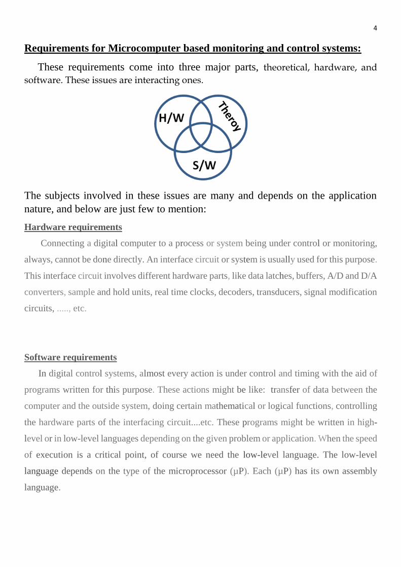
Requirements for Microcomputer based monitoring and control systems:
These requirements come into three major parts, theoretical, hardware, and
software. These issues are interacting ones.
The subjects involved in these issues are many and depends on the application
nature, and below are just few to mention:
Hardware requirements
Connecting a digital computer to a process or system being under control or monitoring,
always, cannot be done directly. An interface circuit or system is usually used for this purpose.
This interface circuit involves different hardware parts, like data latches, buffers, A/D and D/A
converters, sample and hold units, real time clocks, decoders, transducers, signal modification
circuits, ....., etc.
Software requirements
In digital control systems, almost every action is under control and timing with the aid of
programs written for this purpose. These actions might be like: transfer of data between the
computer and the outside system, doing certain mathematical or logical functions, controlling
the hardware parts of the interfacing circuit....etc. These programs might be written in high-
level or in low-level languages depending on the given problem or application. When the speed
of execution is a critical point, of course we need the low-level language. The low-level
language depends on the type of the microprocessor (µP). Each (µP) has its own assembly
language.
5
Theoretical requirements
A) Sampling rate:
Due to the discrete way of digital computers in dealing with signals, as mentioned earlier,
there will be a certain time between processing one sample and another. The minimum period
of this time depends on the time required by the computer to process the sample. On the other
hand, the maximum period can be controlled by us through hardware or software
arrangements. But, of course there is a limitation on this maximum period which we call
sampling period. Shannon criterion states, that the sampling rate of a given signal must be
equal to, or larger than twice the maximum frequency in the signal. Many control books give
the number ten instead of two in order to be on the safe side. If we are talking about systems,
one rough and acceptable way of choosing the sampling period is, to take it ten times smaller
than the smallest time constant for the system.
B) Difference equation:
Dynamic behavior of continuous control systems is described by differential equations,
while in discrete control systems it is described by difference equations.
C) Z-Transformation
The role of this transformation in discrete time systems is similar to the role of Laplace
transformation in continuous time systems. That is here, to convert difference equations into
algebraic ones.
D) Quantization
This term means converting a signal from analog to digital form. Quantizing analog signals
in magnitude, causes error. The error could be reduced by increasing the number of bits used
for digital representation of signals.
E) Data representation
Signals in digital control systems take different formats as it move from one point to
another. And we have to trace and care for these changes (which the signals undergo) in our
design procedure, otherwise, the control will fail for sure.

6
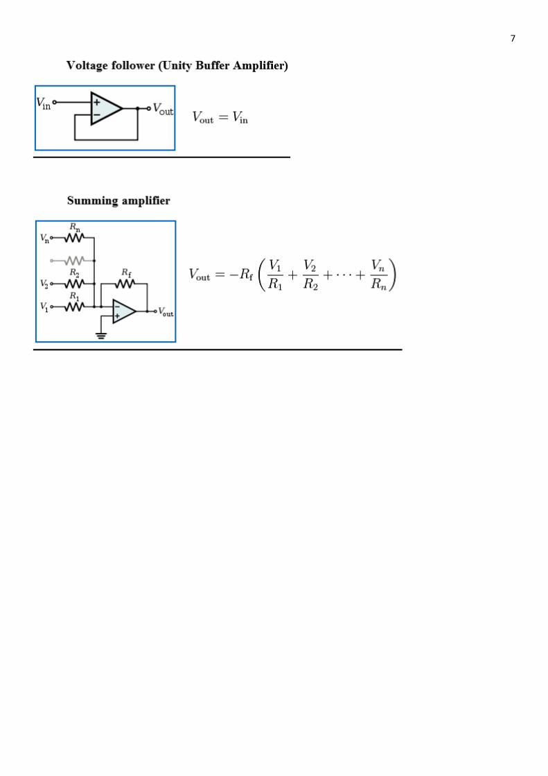
USING OP-AMP FOR SIGNAL MODIFICATION
7

8
COMMUNICATING WITH THE COMPUTER
When using the computer for monitoring and control of a given system,
information will pass in both directions as shown.
This requires the existence of IN and OUT ports in the computer, which is actually
the case. There are many ways of communicating with the compute which come
in two main categories, buses and ports. ISA bus, PCI bus, Parallel port, and Serial
port are examples of such ways. Of course all these ways use connectors or slots
for the actual physical connections. Some of these ways are universal and some
are dedicated. Data are sent or received either in parallel or serial way.
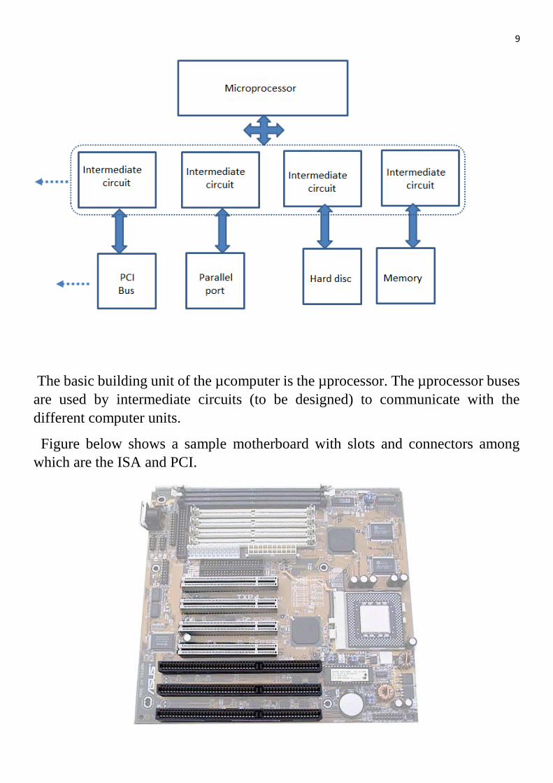
Computer architecture:
Generally the microcomputer consists of the microprocessor, memory, and
input/output units.
It is important to notice that there are many different computer architectures.
Figure below shows just a simple partial clarifying block diagram.
9
The basic building unit of the µcomputer is the µprocessor. The µprocessor buses
are used by intermediate circuits (to be designed) to communicate with the
different computer units.
Figure below shows a sample motherboard with slots and connectors among
which are the ISA and PCI.

10
Bus and I/O Standards:
The microcomputers buses are many, among which are the followings:
[[PCI Express (formerly 3GIO)]] [[InfiniBand (formerly System I/O, NGIO, Future I/O)]] [[
HyperTransport (formerly LDT)]] [[RapidIO]] [[PCI Bus, PCI-X Bus]] [[ISA Bus (Industry
Standard Architecture)]]
[[Plug and Play (PnP)]] [[EISA Bus (Extended Industry Standard Architecture)]][[
VL Bus (VESA Local Bus/Video Electronics Standards Association)
PCMCIA (Personal Computer Memory Card International Association)
[[CardBus (PCMCIA Bus Master)]] [[Micro Channel]]
[[[AGP (Accelerated Graphics Port)]] [[I2O, Intelligent-IO]]
[[USB (Universal Serial Bus)]] [[SMBus (System Management Bus), I2C, ACCESS.bus]]
[[[IrDA (infrared data link)]]
[[IDE, EIDE, ATA, ATA-2, ATAPI, Fast ATA, Ultra ATA, Ultra DMA, DMA/33,
DMA/66, etc.]] [[SCSI (Small Computer Systems Interface)]]
[[RAID (Redundant Array of Inexpensive Disks)]] [[Fibre Channel]]
[[FireWire (IEEE 1394)]] [[HIPPI]] [[HSSI (High Speed Serial Interface)]] [[PC/104]]
[[Multibus]] [[VME Bus]] [[[STD 32 Bus]]
[[CAN Bus (Controller Area Network)]]
11
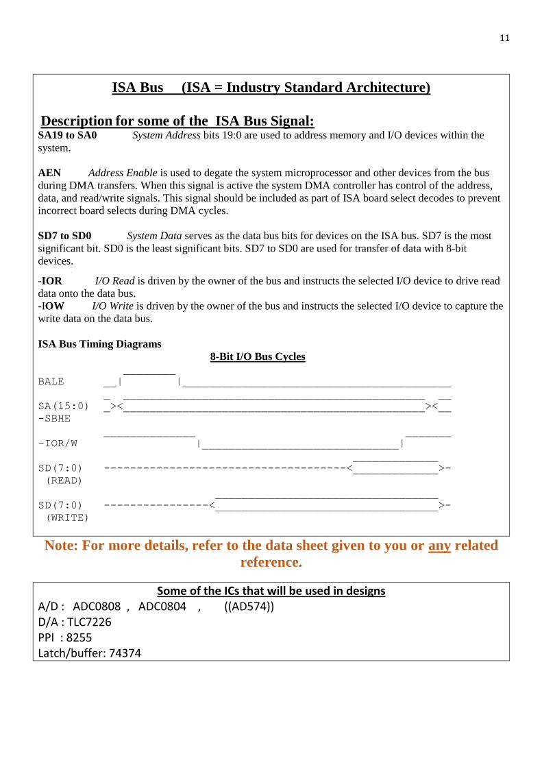
ISA Bus (ISA = Industry Standard Architecture)
Description for some of the ISA Bus Signal: SA19 to SA0 System Address bits 19:0 are used to address memory and I/O devices within the
system.
AEN Address Enable is used to degate the system microprocessor and other devices from the bus
during DMA transfers. When this signal is active the system DMA controller has control of the address,
data, and read/write signals. This signal should be included as part of ISA board select decodes to prevent
incorrect board selects during DMA cycles.
SD7 to SD0 System Data serves as the data bus bits for devices on the ISA bus. SD7 is the most
significant bit. SD0 is the least significant bits. SD7 to SD0 are used for transfer of data with 8-bit
devices. .
-IOR I/O Read is driven by the owner of the bus and instructs the selected I/O device to drive read
data onto the data bus.
-IOW I/O Write is driven by the owner of the bus and instructs the selected I/O device to capture the
write data on the data bus.
ISA Bus Timing Diagrams
8-Bit I/O Bus Cycles ________
BALE __| |_________________________________________
_ ______________________________________________ __
SA(15:0) _><______________________________________________><__
-SBHE
______________ _______
-IOR/W |______________________________|
_____________
SD(7:0) -------------------------------------<_____________>-
(READ)
__________________________________
SD(7:0) ----------------<__________________________________>-
(WRITE)
Note: For more details, refer to the data sheet given to you or any related
reference.
Some of the ICs that will be used in designs A/D : ADC0808 , ADC0804 , ((AD574)) D/A : TLC7226 PPI : 8255 Latch/buffer: 74374

12
ICs: IC1: 8255 PPI (L-notes-ICs-1)(16-10-2017) PPI 8255 pin configuration (Pinout)
8255 Basic operation
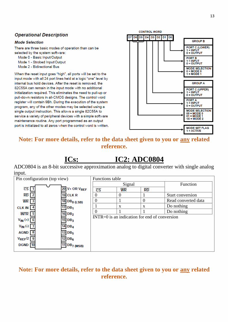
13
Note: For more details, refer to the data sheet given to you or any related
reference.
ICs: IC2: ADC0804 ADC0804 is an 8-bit successive approximation analog to digital converter with single analog
input. Pin configuration (top view)
Functions table
Signal Function
0 0 1 Start conversion
0 1 0 Read converted data
1 x x Do nothing
0 1 1 Do nothing
INTR=0 is an indication for end of conversion
Note: For more details, refer to the data sheet given to you or any related
reference.
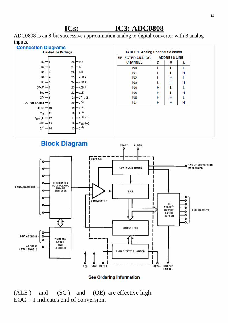
14
ICs: IC3: ADC0808 ADC0808 is an 8-bit successive approximation analog to digital converter with 8 analog
inputs.
(ALE ) and (SC ) and (OE) are effective high.
EOC = 1 indicates end of conversion.

15
Timing diagram
Note: For more details, refer to the data sheet given to you or any related
reference.

16
QUESTIONS – Group 1 Q1- Consider the figure below:
A- In Figure below, if Vd is 80H then what is the value of T in ᵒC? B- Design the modification unit using operational amplifiers.
Q2- Find R1 and R2 in circuit below.
Q3- Derive the equation relating I to Vin in the V to I
converter below.
Q-4- In Figure below, it is intended to input the 12 bits output of the 12 bit latch to the PC using the 8bit ISA
bus with the help of buffers. Complete the design given below, and write a program to input one data group
from the latch to the computer and save it in memory location “TWLV”. (Note: use addresses between 300H
and 30FH and as needed).
Q5- Interface the 74374 in the figure below to the ISA bus as follows:
-The 74374 is to be interfaced to the ISA bus as an output port with address 378H .
- A 7474 D F-F is used to enable or disable the 74374 buffer.(Hint: use address 379H to set the D F-F and
address 37AH to reset the D F-F)
- Write a program in pseudo language to output the value EEH from the PC to the 74374 latch, and to set Q to
one.

17
Q6- The system shown in Fig. below is used to activate a 220v a.c. cooling system if the temperature T
increases above 30°C and turn the system off if the temperature decreases below 20°C. Complete the
system design. Use addresses between 300H and 3FFH. Then write a loop program which checks temperature
and takes the right action.

18
Q7- A- Interface the cct. in Fig. below to the PC using the ISA bus .
B- Design B1 and B3.
C- Write a program in Pseudo Language which does the following procedure:
Inputs a sample of T.
Compares T (in °C) with Td (the desired T) (in °C) to find the error Te (in °C).
Finds Tc which is equal to Te multiplied by 2.
Applies routine ROT1 to find CTRLdig .
Outputs CTRLdig to the D/A conv.

19
Q8- Interface the 8255 PPi to the PC through the ISA bus. Use the addresses 304H – 307H.
And write a program to read data through port A and send it to port B (Considering that the
PPI is already programmed in mode 0, and so that: (port A: I/P) (port B: O/P), and (port C:
o/p).
REFERENCES - Group 1
1-Pc Interfacing, Pei An, 1st ed, Newnes. 1998
2-PC Architecture, Michael Karbo, 1st ed, karbosguide, 2005
3-PC Based Instrumentation and Control, Mike Tooley, 1st ed, Elsevier,
2005