TFS7701-7708 HiperTFS-2 Family - Power · TFS7701-7708 HiperTFS-2 Family April Combined Two-Switch...
42
TFS7701-7708 HiperTFS-2 Family www.power.com April 2015 Combined Two-Switch Forward and Flyback Power Supply Controllers with Integrated High-Voltage MOSFETs ™ This Product is Covered by Patents and/or Pending Patent Applications. Figure 1. Schematic of Two-Switch Forward and Flyback Converter. Product Enhancements • Selectable 132 kHz main switching frequency for lower cost and smaller magnetics • Increased main peak power vs. HiperTFS-1 • Self-biased high-side driver eliminates high-side bias winding and diode • Package lead form and pinout modified for easier insertion and PC-board layout • Tighter UV (ON) standby threshold tolerance • Improved standby no-load performance Key Benefits • Single IC solution for two-switch forward main (66 kHz/132 kHz) and flyback (132 kHz) standby • High integration allows smaller form factor and higher power density designs, with reduced component count • Incorporates control, gate drivers, and three power MOSFETs • Level shift technology eliminates need for pulse transformer • Protection features include: UV, OV, OTP, OVP, standby OPC, SCP, and I LIMIT • Transformer reset control, prevents saturation under all conditions • Main duty cycle operation above 50% for reduced rms currents and lower output diode voltage rating • Less than 10% variation in standby overload power over input voltage range • Up to 586 W peak output power in a highly compact package • >90% efficiency at full load • Simple clip mounting to heat sink without need for insulation pad • Halogen free and RoHS compliant Typical Applications • PC (80 PLUS ® Bronze and 80 PLUS Silver) • Printer • LCD TV • Video game consoles • High-power adapters • Industrial and appliance Output Power Table Product 3 Two-Switch Forward 380 V Flyback 100 V - 400 V Continuous 1 (50 °C) Peak 2 Continuous (50 °C) TFS7701H 148 W 187 W 20 W TFS7702H 190 W 297 W 20 W TFS7703H 229 W 375 W 20 W TFS7704H 251 W 419 W 20 W TFS7705H 269 W 466 W 20 W TFS7706H 298 W 513 W 20 W TFS7707H 322 W 553 W 20 W TFS7708H 343 W 586 W 20 W Table 1. Output Power Table. Notes: 1. Maximum practical continuous power in an open frame design with adequate heat sinking to maintain a heat sink temperature ≤95 ºC (see Key Applications Considerations for more information) measured at specified ambient temperature. 2 Peak load less than 10 seconds and average power less than maximum continuous load. 3. Package: eSIP-16F. (Note: Direct attach to heat sink, does not require insulation SIL pad). HD DC Input (VDC) Main Output Standby Output RTN G S HiperTFS-2 VDDH L FB FB EN EN BP DSB EN FB Control, Gate Drivers, Level Shift R D HS PI-7078-082213 Two-Switch Forward Transformer Standby Flyback Transformer *Simplified feedback circuit * * * * + Figure 2. Package Option. eSIP-16F (H Package)
Transcript of TFS7701-7708 HiperTFS-2 Family - Power · TFS7701-7708 HiperTFS-2 Family April Combined Two-Switch...
TFS7701-7708HiperTFS-2 Family
www.power.com April 2015
Combined Two-Switch Forward and Flyback Power Supply Controllers with Integrated High-Voltage MOSFETs
™
This Product is Covered by Patents and/or Pending Patent Applications.
Figure 1. Schematic of Two-Switch Forward and Flyback Converter.
Product Enhancements
• Selectable 132 kHz main switching frequency for lower cost and smaller magnetics
• Increased main peak power vs. HiperTFS-1• Self-biased high-side driver eliminates high-side bias winding
and diode• Package lead form and pinout modified for easier insertion and
PC-board layout• Tighter UV(ON) standby threshold tolerance• Improved standby no-load performance
Key Benefits• Single IC solution for two-switch forward main (66 kHz/132 kHz)
and flyback (132 kHz) standby• High integration allows smaller form factor and higher power
density designs, with reduced component count• Incorporates control, gate drivers, and three power MOSFETs• Level shift technology eliminates need for pulse transformer• Protection features include: UV, OV, OTP, OVP, standby OPC,
SCP, and ILIMIT
• Transformer reset control, prevents saturation under all conditions• Main duty cycle operation above 50% for reduced rms currents
and lower output diode voltage rating• Less than 10% variation in standby overload power over input
voltage range
• Up to 586 W peak output power in a highly compact package• >90% efficiency at full load• Simple clip mounting to heat sink without need for insulation pad• Halogen free and RoHS compliant
Typical Applications• PC (80 PLUS® Bronze and 80 PLUS Silver)• Printer • LCD TV • Video game consoles • High-power adapters• Industrial and appliance
Output Power Table
Product3
Two-Switch Forward380 V
Flyback100 V - 400 V
Continuous1
(50 °C) Peak2 Continuous(50 °C)
TFS7701H 148 W 187 W 20 W
TFS7702H 190 W 297 W 20 W
TFS7703H 229 W 375 W 20 W
TFS7704H 251 W 419 W 20 W
TFS7705H 269 W 466 W 20 W
TFS7706H 298 W 513 W 20 W
TFS7707H 322 W 553 W 20 W
TFS7708H 343 W 586 W 20 W
Table 1. Output Power Table. Notes:1. Maximum practical continuous power in an open frame design with adequate
heat sinking to maintain a heat sink temperature ≤95 ºC (see Key Applications Considerations for more information) measured at specified ambient temperature.
2 Peak load less than 10 seconds and average power less than maximum continuous load.
3. Package: eSIP-16F. (Note: Direct attach to heat sink, does not require insulation SIL pad).
HD
DC Input(VDC)
MainOutput
StandbyOutput
RTN
G S
HiperTFS-2 VDDH
L
FB
FB
EN
EN
BP
DSB
EN FB
Co
ntro
l, G
ate
Dri
vers
, Lev
el S
hift
R
D
HS
PI-7078-082213
Two-SwitchForward
Transformer
Standby FlybackTransformer
*Simplied feedback circuit
* *
* *
+
Figure 2. Package Option.
eSIP-16F (H Package)

Rev. B 04/15
2
TFS7701-7708
www.power.com
Section List
Description .................................................................................................................................................................. 3
Product Highlights ...................................................................................................................................................... 3
Pin Functional Description ......................................................................................................................................... 5 Pin Configuration ...................................................................................................................................................... 5 Functional Block Diagram .....................................................................................................................................6-7
Functional Description ............................................................................................................................................... 8
Design, Assembly and Layout Considerations ..................................................................................................... 14
Layout Considerations .............................................................................................................................................. 17
Transformer Secondary and Output Diodes ........................................................................................................... 21
Main Converter Typical Waveforms ......................................................................................................................... 22
Quick Design Checklist ............................................................................................................................................. 23
Design Example ......................................................................................................................................................... 25
Absolute Maximum Ratings ..................................................................................................................................... 27
Parameter Table ..................................................................................................................................................... 27
Package Details ........................................................................................................................................................ 34
Part Ordering Information......................................................................................................................................... 40
Part Marking Information ......................................................................................................................................... 41

Rev. B 04/15
3
TFS7701-7708
www.power.com
Description The HiperTFS-2 device family members incorporate both a high-power two-switch-forward converter and a mid-power flyback (standby) converter into a single, low-profile eSIP™ power package. The single chip solution provides the controllers for the two-switch-forward and flyback converters, high- and low-side drivers, all three of the high-voltage power MOSFETs, and eliminates the converter’s need for costly external pulse transformers. The device is ideal for high power applications that require both a main power converter (two-switch forward) up to 586 W peak, and standby converter (flyback) up to 20 W. HiperTFS-2 includes Power Integrations’ standard set of comprehensive protection features, such as integrated soft-start, fault and overload protection, and hysteretic thermal shutdown. HiperTFS-2 utilizes advanced power packaging technology that simplifies the complexity of two-switch forward layout, mounting and thermal management, while providing very high power capabilities in a single compact package. The devices operate over a wide input voltage range, and can be used following a power-factor correction stage such as HiperPFS. Two-switch-forward power converters are often selected for applications demanding cost-effective converters that have high efficiency, fast transient response, and high rejection to line voltage variation. The two-switch-forward controller incorporated into HiperTFS-2 devices improves on the classic topology by allowing operation considerably above 50% duty cycle. This improvement reduces RMS current conduction losses, minimizes the size and cost of the bulk capacitor, and minimizes output diode voltage ratings. The advanced design also includes transformer flux reset control (saturation protection) and charge-recovery switching of the high-side MOSFET, which reduces switching losses. This combination of innovations yields an extremely efficient power supply with smaller MOSFETs, fewer passives and discrete components, and a lower-cost smaller transformer.
HiperTFS-2’s flyback standby controller and MOSFET solution is based on the highly popular TinySwitch™ technology used in billions of power converter ICs due to its simplicity of operation, light load efficiency, and rugged, reliable, performance. This flyback converter can provide up to 20 W of output power and the built-in overload power compensation reduces component design margin.
Product Highlights
Protected Two-Switch Forward and Flyback Combination Solution• Incorporates three high-voltage power MOSFETs, main and
standby controllers, and gate drivers • Level shift technology eliminates need for pulse transformer• Programmable line undervoltage (UV) detection prevents
turn-off glitches• Programmable line overvoltage (OV) detection; latching and
non-latching
• Accurate hysteretic thermal shutdown (OTP)• Accurate selectable cycle-by-cycle current limit (main and
standby)• Line compensated standby MOSFET current limit for
standby over power compensation (OPC) • Fully integrated soft-start to minimize start-up stress • Simple fast AC reset• Reduced EMI
• Synchronized 66/132 kHz forward and 132 kHz flyback converters
• Frequency jitter • Eliminates up to 30 discrete components for higher reliability
and lower cost
Asymmetrical Two-Switch Forward Reduces Losses• Allows >50% duty cycle operation
• Reduces primary-side RMS currents and conduction losses• Minimizes the size and cost of the bulk capacitor• Allows reduced capacitance or longer hold-up time• Allows lower voltage output diodes for higher efficiency
• Transformer reset control• Prevents transformer saturation under all conditions• Extends duty cycle to satisfy AC cycle drop out ride through
• Duty cycle soft-start• Satisfies 2 ms ~ 20 ms start-up with large capacitance at
output• Self-biased high-side driver eliminates high-side bias winding
(66 kHz)• Remote-on/off function • Voltage-mode controller with current limit
20 W Flyback with Selectable Power Limit• TinySwitch-III based converter • Selectable power limit (10 W, 12.5 W, 15 W, 20 W) • Built-in overload power compensation (OPC)
• Flat overload power vs. input voltage• Reduces component stress during overload conditions• Reduces required design margin for transformer and output
diode • Output overvoltage (OVP) protection with fast AC reset
• Latching, non-latching, or auto-restart • Output short-circuit protection (SCP) with auto-restart
Advanced Package for High Power Applications • Up to 586 W peak output power capability in a highly
compact package • Simple clip mounting to heat sink
• Can be directly connected to heat sink without insulation pad• Provides lower thermal resistance than a TO-220• Heat slug connected to ground potential for low EMI
• Two row lead form for easy insertion into PC-board • Single power package for two power converters reduces
assembly costs and layout size

Rev. B 04/15
4
TFS7701-7708
www.power.com
Table 2. Summary of Differences Between HiperTFS-2 and Other Typical High Power Supplies.
Function Typical Two-Switch Forward HiperTFS-2 Advantages of HiperTFS-2
Nominal Duty Cycle 33% 45%Wider duty cycle reduces RMS switch currents by 17%.Reduces RDS(ON) losses by 31%
Maximum Duty Cycle <50% 63%
Switch Current (RMS) 100% 83%
Output Catch Diode Voltage Rating
100% 79%Lower losses. Wider DMAX lowers catch diode rating by VO + VD/DMAX reduction in catch diode voltage rating
Clamp VoltageReset diodes from zero
to VIN
Reset from zero to (VIN + 130 V)
With fast/slow diode combination, allows charge recovery to limit high-side MOSFET COSS loss
Thermal Shutdown ---118 °C Shutdown /
55 °C HysteresisHiperTFS-2 provides integrated OTP device protection
Current Sense Resistor0.5 V drop
(0.33 W at 300 W)No sense resistor
Improved efficiency. MOSFET RDS(ON) sense eliminates need for sense resistor
High-Side DriveRequires gate-drive
transformer (high-cost)Built-in high-side drive
Lower cost; component elimination. Removes high-cost gate-drive transformer (EE10 or toroid)
Component Count Higher Lower Saves up to 30 components, depending on specification.
TinySwitch Overload Power Compensation vs. Input Voltage
--- Built-in compensationSafer design; easier to design power supply. Flattens standby overload output power versus line voltages
Package PC BoardCreepage
TO-220 = 1.17 mm eSIP16/12 = 2.3 mmHiperTFS-2 meets functional safety spacing at package pins
Package Assembly
2 × TO-220 package, 2 × SIL (insulation),1 main controller,
1 standby controller
1 Package No SIL (insulation) pad required

Rev. B 04/15
5
TFS7701-7708
www.power.com
Pin Functional Description
MAIN DRAIN (D) PinDrain of the low-side MOSFET transistor forward converter.
STANDBY DRAIN (DSB) PinDrain of the MOSFET of standby power supply.
GROUND (G) PinThis pin gives a signal current path to the substrate of the low-side controller. This pin is provided to allow a separate Kelvin connection to the substrate of the low-side controller to eliminate inductive voltages that might be developed by high switching currents in the SOURCE pin. The GROUND pin is not intended to carry high currents, it is intended as a voltage-reference connection only.
SOURCE (S) PinSOURCE pin that is common to both the standby and main supplies.
RESET (R) PinThis pin provides information to limit the maximum duty cycle as a function of the current fed into the LINE-SENSE and RESET pins to prevent cycle-by-cycle saturation of main transformer. This pin can also be pulled up to bypass to signal remote-on/off of the main converter only.
ENABLE (EN) PinThis is the ENABLE and CURRENT LIMIT SELECTION pin for the standby controller. Prior to start-up the resistor value connected from ENABLE to BYPASS, is detected to select one of several internal standby current limit values.
LINE-SENSE (L) PinThis pin provides input bulk voltage line-sense function. This information is used by the undervoltage and overvoltage detection circuits for both main and standby. The pin can also be pulled up to BYPASS or be pulled down to SOURCE to implement a remote-on/off of both standby and main supplies simultaneously. The LINE-SENSE pin works in conjunction with the RESET pin to implement a duty cycle limit function. The LINE-SENSE pin compensates the value of standby current limit so as to flatten the output overload power characteristic as a function of input voltage.
FEEDBACK (FB) PinThis pin provides feedback for the main two transistor forward converter. An increase in sink current from the FEEDBACK pin to ground, reduces the operating duty cycle. This pin also selects the main device current limit at start-up (in a similar manner to ENABLE pin).
BYPASS (BP) PinThis is the decoupled operating voltage pin for the low-side controller. At start-up the capacitor connected to this pin is charged from an internal current source. During normal operation the capacitor voltage is maintained by drawing current from the low-side bias winding on the standby power supply. This pin is also used to implement remote-on/off for the main controller. This is done by driving extra current into the BYPASS pin when we want to turn-on the main controller. The BYPASS pin also implements a latch-off function to disable standby and main when the BYPASS pin current exceeds a threshold. The latch is reset when LINE-SENSE pin falls below UV (off) standby threshold. The BYPASS pin capacitor value selects for either 66 kHz (1 mF) or 132 kHz (10 mF) main switching frequency.
HIGH-SIDE OPERATING VOLTAGE (VDDH) PinThis is the high-side bias (VDD) of approximately 11.5 V. This voltage is maintained with current from an internal high-voltage current source and/or from a bootstrap diode from the low-side standby bias supply.
HIGH-SIDE SOURCE (HS) PinSOURCE pin of the high-side MOSFET.
HIGH-SIDE DRAIN (HD) PinDRAIN pin of the high-side MOSFET. This MOSFET is floating with respect to low-side source and ground.
Figure 2. Pin Configuration.
PI-6774-030713
16D DS
B
G S R EN
HD
HD
HS
S S
L FB HS
HD
VD
DH
BP
1413101191 3 5 6 7 8
H Package (eSIP-16F)
Exposed Pad(Backside) InternallyConnected to SOURCE Pin (see eSIP-16FPackage Drawing)
Exposed Metal(On Edge) InternallyConnected

Rev. B 04/15
6
TFS7701-7708
www.power.com
PI-5263-021511
PWMCOMPARATOR
PWMINPUT THERMAL SD
CONTROLLEDTURN-ON
GATE DRIVER
CURRENT LIMITCOMPARATOR
SOURCE (S)
S
R
Q
-
+
BYPASS (BP)
LINE-SENSE (L)
RESET (R)
FEEDBACK (FB)and MAIN CURRENT
LIMIT SELECT
STOP
HSD1 HSD2
FAULT PRESENT
LV SAWD2MAX CLK2
MAIN REMOTE-ON
+
-
LEADINGEDGE
BLANKING
R
L
DUTYCYCLELIMIT
DMAX
GATE
CLK
ON
DRAIN (D)
VBG
LINESENSE
LV
POWER ONILIMIT
SELECT
VILIMIT
DSSSOFT-START
PWM INPUT
REMOTEOFF
REMOTE OFF
GATEHS
3 V+VT
Figure 3. Functional Block Diagram for Two-Switch Forward Converter.
HIGH-SIDE OPERATING VOLTAGE (VDDH)
HSD1
HSD2
12 V11.5 V10.5 V
HIGH-SIDEDRAIN (HD)
HIGH-SIDESOURCE (HS)
VDDHUNDERVOLTAGE
PI-6912-032813
+
DISCRIMINATOR
VOLTAGEREGULATOR
12 V
S
R
Q
Rev. B 04/15
7
TFS7701-7708
www.power.com
Figure 4. Functional Block Diagram for Flyback/Standby Converter.
PI-6968-060413
CLOCKCLK2
5.7 V4.7 V
SOURCE (S)
S
R
Q
DCMAX
D2MAX
SAW
BYPASS (BP)
ENABLE (EN)and STANDBY
CURRENT LIMITSELECT
+
-
VILIMIT
FAULTPRESENT
CURRENT LIMITCOMPARATOR
ENABLE
LEADINGEDGE
BLANKING
THERMALSHUTDOWN
+
-
STANDBY DRAIN (DSB)
BYPASS PINUNDERVOLTAGE
LV (LINE VOLTAGE)
SAW D2MAX
CLK2 FAULTPRESENT
OSCILLATOR
THERMAL SD
3 V + VT
Q
115 µA
RESET
AUTO-RESTARTCOUNTER
JITTER
1.0 V
6.0 V
ENABLE PULLUP RESISTORSELECT AND
CURRENTLIMIT STATE
MACHINE
MAINREMOTE-
ON/OVP
LATCH OFF
VINILIMIT
ADJUST
MAINREMOTE-ON
REGULATOR5.7 V

Rev. B 04/15
8
TFS7701-7708
www.power.com
Functional Description
The HiperTFS-2 contains two switch-mode power supply controllers and associated low-side MOSFET’s along with high-side driver and high-side MOSFET.
• The HiperTFS-2 two-switch forward includes a controller along with low-side power MOSFET, high-side power MOSFET, high-side driver and selectable main switching frequency (synchronous with standby) of 66/132 kHz. The main converter operates in voltage-mode (linear duty cycle control) at fixed frequency (exactly half the operating frequency of the standby controller when is 66 kHz mode). The control converts a current input (FEEDBACK pin), to a duty cycle at the open drain MOSFET MAIN DRAIN pin decreasing duty cycle with increasing sourced current from the FEEDBACK pin.
• The HiperTFS-2 fixed frequency (132 kHz) standby flyback includes a controller and power MOSFET which is based on TinySwitch-4. This device operates in multi-level ON/OFF current limit control mode. The open drain MOSFET (STAND-BY DRAIN pin) is turned on when the sourced current from the ENABLE pin is below the threshold and switching is disabled when the ENABLE pin current is above the threshold.
In addition to the basic features, such as the high-voltage start-up, the cycle-by-cycle current limiting, loop compensation circuitry, auto-restart and thermal shutdown, the HiperTFS-2 main controller incorporates many additional functions that reduce system cost, increase power supply performance and design flexibility.
Main Converter General IntroductionThe main converter for the HiperTFS-2, is a two-switch forward converter (although the HiperTFS-2 could be used with other two-switch topologies). This topology involves a low-side and high-side power MOSFET, both of which are switched at the same time. In the case of the HiperTFS-2, the low-side MOSFET is a 725 V MOSFET (with the substrate connected to the SOURCE pin). The high-side MOSFET is a 530 V MOSFET (with the substrate connected to the HIGH-SIDE DRAIN (HD) pin). As such the substrate of both low-side and high-side MOSFET’s are tied to quiet circuit nodes (0 V and VIN respectively), meaning that both MOSFETs have electrically quiet substrates – good for EMI.
The low-side MOSFET has a very low COSS capacitance and thus can be hard-switched without performance penalty. Due to the external clamp configuration it is possible to substantially soft-switch the high-side MOSFET at high-loads (thus eliminating a large proportion of high-side capacitive switching loss) and improving efficiency. The higher breakdown voltage on the low-side MOSFET allows the transformer reset voltage to exceed the input voltage, and thus allow operation at duty cycles greater than 50%. Higher duty cycle operation leads to lower RMS switch currents and also lower output diode voltage-rating, both of which contribute to improved efficiency.
The HiperTFS-2 also contains a high-side driver to control the high-side MOSFET. This external bootstrap diode (or internally
self-biased) high-side driver eliminates the need for a gate-driver transformer, an expensive component that is required for many other two-switch forward circuits.
Main Start-Up OperationOnce the flyback (standby) converter is up and running, the main converter can be enabled by two functions. The first condition is that the BYPASS pin remote-on current must exceed the remote-on threshold (IBP(ON)), provided by an external remote-on/off circuit. This current threshold has a hysteresis to prevent noise interference. Once the BYPASS remote-on has been achieved, the HiperTFS-2 also requires that the LINE-SENSE pin current exceeds the UV main-on (IL(MA-UVON)), which corresponds to approximately 336 VDC input voltage when using a 4 MW LINE-SENSE pin resistor. Once this LINE-SENSE pin threshold has been achieved the HiperTFS-2 will enter a 60 ms pre-charge period (tD(CH)) to allow the PFC-boost stage to reach
Figure 5. Switching Frequency Jitter (Idealized VDRAIN Waveforms).
PI-
4530
-041
107
fOSC -
4 ms
Time
SwitchingFrequency
VDRAIN
fOSC +
Figure 6. Supply Start-Up Sequence by Remote-On.
VIN
StandbyOutput
MainOutput
60 ms
385 V
MainPrimaryCurrent
Remote ON
t
t
t
t
t
PI-6775-022113

Rev. B 04/15
9
TFS7701-7708
www.power.com
regulation before the main applies a load to the bulk-capacitor. Also during this pre-charge period the high-side driver is charged via the bootstrap diode (or self bias) from the low-side auxiliary voltage, and is charged when the main low-side MOSFET turns on, while the main high-side MOSFET is held off. By the end of the pre-charge period, the PFC-boost voltage should be at or above the nominal boost voltage. The HiperTFS-2 begins switching, going through the soft-start period (tSS). During the soft-start period the maximum duty cycle starts at 30% and is ramped during a 12 ms period to the maximum. The ramped duty cycle controls the rise slew rate of the output during start-up, allowing well controlled start-up and also facilitates a smooth transition when the control loop takes over regulation towards the end of soft-start. This allows the main to start-up within the required period for the application (typically <20 ms for PC main applications), when there is a substantial capacitive load on the output.
Main Converter Control FEEDBACK (FB) Pin OperationThe FEEDBACK pin is the input for control loop feedback from the main control loop. During normal operation the FEEDBACK pin is used to provide duty cycle control for the main converter. The system output voltage is detected and converted into a feedback current. The main converter duty cycle will reduce as more current is sourced from the FEEDBACK pin, reaching zero duty cycle at approximately 2.1 mA. The nominal voltage of the FEEDBACK pin is maintained at approximately 3.5 V. An internal pole on the FEEDBACK pin is set to approximately 12 kHz, in order to facilitate optimal control loop response.
The maximum duty cycle of the main converter is defined by the LINE-SENSE pin and RESET pin behavior and is a dynamically calculated value according to cycle-by-cycle conditions on the LINE-SENSE pin and RESET pin.
Main High-Side DriverThe high-side driver is a device that is electrically floating at the potential of the HIGH-SIDE MOSFET SOURCE (HS) pin. This device provides gate-drive for the high-side main MOSFET. The low-side main and high-side main MOSFET’s switch simultaneously. The high-side driver has a HIGH-SIDE OPERATING VOLTAGE supply pin. External circuitry or an internal source, provides operating current and provides HIGH-SIDE OPERATING VOLTAGE pin. The high-side operating voltage has an internal
12 V shunt-regulator. The device consumes approximately 2.3 mA when driving the high-side MOSFET.
The HIGH-SIDE OPERATING VOLTAGE pin has an undervoltage lock-out threshold, to prevent gate-drive when the supply voltage drops below a safe threshold. At power-up the high-side driver remains in the off-state, until the HIGH-SIDE OPERATING VOLTAGE pin is charged above 10.5 V, at which point the high-side driver becomes active. The high-side driver is initially charged via either a bootstrap diode connected to the HIGH-SIDE OPERATING VOLTAGE pin from the low-side standby auxiliary supply (approximately 12 V) or from an internal high-voltage current source. During start-up the high-side MOSFET remains off, but the low-side MOSFET is turned on for a period of 60 ms to allow pre-charge of the high-side operating voltage to 12 V. After this period, the high-side operating voltage is supplied by a bootstrap diode or internal current source.
Once the high-side driver is operating it receives level-shifted drive commands from the low-side device. These drive commands cause both turn-on and turn-off drive of the high-side main MOSFET simultaneously with that of the low-side main MOSFET.
The high-side driver also contains a thermal shutdown on-chip, but this is set to a temperature above the thermal shutdown temperature of the low-side device. Thus the low-side will always shutdown first.
Main Converter Maximum Duty CycleThe LINE-SENSE pin resistor converts the input voltage into an LINE-SENSE pin current signal. The RESET pin resistor converts the reset voltage into an RESET pin current signal. The LINE-SENSE pin and RESET pin currents allow the HiperTFS-2 to determine a maximum duty cycle envelope on a cycle-by-cycle basis. This feature ensures sufficient time for transformer reset on a cycle-by-cycle basis and also protects against single-cycle transformer saturation and at high-input voltage by limiting the maximum duty cycle to prevent the transformer from reaching an unsafe flux density during the on-time period. Both of these features allow the optimal performance to be obtained from the main transformer. The duty cycle limit is trimmed during production.
The LINE-SENSE pin and RESET pin are sampled just before the turn-on of the next main cycle. This is done to sample at a point when there is minimal noise in the system. Due to the low current signal input to the LINE-SENSE pin and RESET pin, care should be taken to prevent noise injection on these pins (see Applications section layout guidelines for details).
Main On-Chip Current Limit with External SelectionDuring start-up, the FEEDBACK pin and ENABLE pin are both used to select internal current limits for the main and standby converters respectively. The detection period occurs at the initial start-up of the device, and before the main or standby MOSFETs start switching. This is done to minimize noise interference.
Figure 7. PWM Duty Cycle vs. Control Current.
61%
70%
0%
1.1 mA 2.1 mA
Duty (D)
FEEDBACK PinSink Current IFB
IL = 90 µAIR = 170 µA
Typical IL and IRcurrents at VMIN
PI-6913-053113
Limited by L and Rpin duty limit

Rev. B 04/15
10
TFS7701-7708
www.power.com
A resistor RFB is connected from the BYPASS pin to the FEEDBACK pin. This resistor feeds current into the FEEDBACK pin (pin voltage is clamped to approximately 1 V during this detection period). The current into the FEEDBACK pin is determined by the value of the resistor, and thus the input current (and indirectly the resistor value), select an internal current limit according to the following table.
Main Line Undervoltage Detection (UV)The LINE-SENSE pin resistor is connected to VIN and generates a current signal proportional to VIN. The LINE-SENSE pin voltage is held by the device at 1.2 V. The LINE-SENSE pin current signal is used to trigger under/overvoltage thresholds for both the standby and main converters. Assuming a LINE-SENSE pin resistor of 4 MW, the standby will begin operating when the LINE-SENSE pin current exceeds the (IL(SB-UVON)) threshold, nominally approximately 100 V. However the main is still held in the off-state, until the LINE-SENSE pin current exceeds the (IL(MA-UVON)) threshold, nominally 336 V for 4 MW. There is hysteresis for both main and standby undervoltage-off thresholds, to allow sufficient margin to avoid accidental triggering, and to provide sufficient margin to meet hold-up time requirements. Bear in mind that the main converter may start to loose regulation before it finally shuts down. This is because the dynamic duty cycle limit may clamp the duty cycle below that required for regulation at lower input voltages. Once the input voltage falls below the 215 V (IL(MA_UVOFF)) threshold, the main will shutdown but standby will continue to operate. The standby will turn off when the input voltage drops below approximately 40 V (IL(SB-UVON)).
Figure 9. Current Limit Selection.
Table 3. FEEDBACK Pin Main Current Limit Selection.
IFB
(Threshold)ILIMIT (Main)
RFB(SELECT)
(1%)
0.0 - 5.1 mA L1 70% mA Open kW
5.1 - 11.9 mA L2 90% mA 511.0 kW
11.9 - 23.8 mA L3 100% mA 232.0 kW
UV(ON)STANDBY, I(L) = 25 µA
4.7 V
1 V
5.7 V
I(L)
V(BP)
V(FB)
V(EN)
TSELECT - current limit selection occurs here duringdevice start-up and before power supply switching
2.7 V
2.7 V
6.0 V afterstandbyacheivesregulation
PI-6973-022513
Figure 8. Duty Cycle Limit vs. Ratio of R Pin Current Over L Pin Current.
0.5 1.0 1.5 2.0 3.02.5
IR/IL
Du
ty C
ycle
Lim
it
0.7
0.6
0.5
0.4
PI-
5977
-061
010
IL = 60 µA
IL = 90 µA
IL = 100 µA
IL = 115 µA

Rev. B 04/15
11
TFS7701-7708
www.power.com
Main Reset Overvoltage DetectionThere is also an overvoltage threshold for the RESET pin. When triggered, the RESET overvoltage will shutdown only the main, leaving the standby in operation.
Standby Power General IntroductionThe standby is a wide range power supply, typically a flyback converter, operating over a wide input range (85-265 VAC) and delivering up to 20 W continuous output power. The standby power supply provides two functions in most high-power applications. It provides a direct secondary output but also provide bias power to other primary-side devices (in particular typically a PFC boost converter).
The HiperTFS-2 standby retains most features of the TinySwitch-III, such as auto-restart, thermal shutdown, multi-level current limit ON/OFF control, etc. The HiperTFS-2 standby controller has a few differences versus TinySwitch-III:1. There are 4 current limits that are selected via the ENABLE
pin (rather than by using different BYPASS pin capacitors as in TinySwitch-III). There are 4 user selectable current limits 500, 550, 650, 750 mA design for secondary standby output power of 10, 12.5, 15 and 20 W.
2. Secondary OVP latching shutdown. This is triggered via a current in excess of the BYPASS pin latching shutdown threshold (IBP(SD) = 15 mA).
3. Dedicated LINE-SENSE pin for line-voltage detection providing absolute UV and OV ON/OFF thresholds (unlike TinySwitch-4 which detects input voltage only during restart). Also higher accuracy for UV(ON) threshold.
4. Current limit is compensated as a function of input voltage to maintain a flat overload characteristic versus input voltage.
In a high-power system, the standby power supply is the first power supply to begin operating. The main converter cannot begin working until the standby is in operation. Likewise the main converter will shutdown at a higher-voltage than the standby and thus the standby is always the last power supply to shutdown.
Standby On-Chip Current Limit with External SelectionDuring start-up, the FEEDBACK pin and ENABLE pin are both used to select internal current limits for the main and standby converters respectively. The detection period occurs at the initial start-up of the device (just after BYPASS pin voltage of 4.7 V is achieved), and before the main or standby MOSFETs start switching. This is done to minimize noise interference.
The ENABLE pin works in a similar way to the FEEDBACK pin selection. The ENABLE pin is clamped to 1 V during selection, during the detection period. Thus the selection resistor values are the same for the ENABLE pin and the FEEDBACK pin. The ENABLE pin internal current selection is chosen according to the above table.
Figure 10. Main and Standby Start-Up.
I EN(Threshold) ILIMIT (Standby) R EN (Select)
(1%)
0 - 5 mA L1 500 mA Open kW
5 - 12 mA L2 550 mA 511 kW
12 - 24 mA L3 650 mA 232 KW
24 - 48 mA L4 750 mA 107 kW
Table 4. ENABLE Pin Standby Current Limit Selection.
VIN
Supply Start-Up Sequence
StandbyOutput
MainOutput
VBP
60 ms
385 V
336 V
100 V
30 V
2-20 ms
6.0 V
4.7 V5.7 V
PI-6776-021513
Figure 11. L and R Pin Duty Limit Mode.
VIN
StandbyOutput
MainOutput
385 V
300 V
212 V
40 V
PI-6974-022813
tHOLDUP ≥ 20 ms
Typically turned off bysecondary supervisorcircuit, once regulation below limit
t1 t2 t3 t4
RL RR
To VINTo Clamp Reset Circuit
R
Hip
erT
FS
L

Rev. B 04/15
12
TFS7701-7708
www.power.com
The current limit selection for both FEEDBACK pin and ENABLE pin takes place when the BYPASS pin first reaches 4.7 V. Once the short detection period is complete, the BYPASS pin is ramped on up to 5.7 V, and the FEEDBACK pin is allowed to float to it’s nominal voltage of 3.5 V.
Standby Line Compensated Current Limit to Flatten Output Overload PowerFor many power supplies, the power output capability of the power supply increases dramatically as the input voltage increases. This means that most power supplies are able to deliver much more power (up to 30-40% more power), into a fault overload when operating at higher input voltage (versus operating at lower input voltage). This can cause a problem since many specifications require that the output overload power capability of the device is more tightly managed. In the case of the HiperTFS-2, the standby current limit is adjusted as a function of line (input voltage), in such a ways as to always provide substantially the same maximum overload power capability. The input voltage is detected via the LINE-SENSE pin current and the internal standby current limit of the device is adjusted accordingly on a cycle-by-cycle basis. This means that the HiperTFS-2 standby will only deliver approximately 5% more overload power at high-line as it did at low-line. This feature provides a much safer design.
Standby Line Undervoltage Detection (UV)The LINE-SENSE pin resistor is connected to VIN and generates a current signal proportional to VIN. The LINE-SENSE pin voltage is held by the device at 1.2 V. The LINE-SENSE pin current signal is used to trigger under/overvoltage thresholds for both the standby and main converters. Assuming a LINE-SENSE pin resistor of 4 MW, the standby will begin operating at approximately 100 V (as defined by IL(SB_UVON)). The standby will shutdown if regulation is lost when input voltage is below 100 V. However the standby will be forced to shutdown if this input voltage drops below approximately 40 V (as defined by IL(SB-UVOFF)).
Main and Standby Oscillator and Switching FrequencyThe standby converter operates at a frequency of 132 kHz. When in 66 kHz mode, main converter operates at exactly half that frequency. The two converters both include a common frequency jitter profile that varies the switching frequency ±4 kHz for the main (twice the jitter frequency range ±8 kHz for the standby), during a 4 ms jitter period. The frequency jitter helps reduce quasi-peak and average EMI emissions.
The HiperTFS-2 main switch frequency is selected at start-up for 66 kHz or 132 kHz based on the value of the BYPASS pin capacitor
It should be noted that when the HiperTFS-2 is running at 66 kHz there is a collision avoidance scheme in which the main converter is the master and the standby is the slave, which avoids the main and standby switching at exactly simultaneous moments. The most common condition would be close to 50% duty cycle, if the main (master) is about to switch (turn-off), then the standby (slave), waits for short instant (200 ns) before starting it’s next cycle. The standby is used as the slave, since the ON/OFF control of the HiperTFS-2 standby is less easily disrupted by sudden delays in switching, versus the linear control loop of the main converter. This collision avoidance is not required when both standby and main run at 132 kHz.
Standby and Main Thermal ShutdownThe HiperTFS-2 provides a thermal shutdown function, (OTP) that protects the HiperTFS-2. This hysteretic thermal shutdown allows the device to automatically recover from any thermal fault event. The thermal shutdown is triggered at a die-temperature of approximately 118 °C and has a high hysteresis to ensure the average device temperature is within safe levels. In a well designed system the HiperTFS-2 thermal shutdown is not triggered during any normal operation and is only present as a safety feature to protect against abnormal or fault conditions.
BYPASS (BP) Pin OperationThe BYPASS (BP) pin is the supply pin for the entire HiperTFS-2 device. The BYPASS pin is internally connected to a high-voltage current source via the STANDBY DRAIN power MOSFET. This high-voltage source will charge the BYPASS pin to 4.7 V during initial power-up. Once the BYPASS pin reaches 4.7 V, the BYPASS pin will check the main and standby current limit selection (FEEDBACK pin and ENABLE pin resistors respectively). This selection takes a very short period, thereafter the BYPASS pin continues being charged until it reaches 5.7 V. During this change the value of the BYPASS pin capacitor is determined. The value selects for main switching frequency of (1 mF = 66 kHz) and 10 mF = 132 kHz) on completion of frequency selection, the standby power supply is ready to begin operation. Like the TinySwitch-4 the high-voltage current source will continue to charge the BYPASS pin if it drops below 5.7 V. However in most typical applications, a resistor (typically 7.5 kW) is connected from primary bias (12 V) to the BYPASS pin. This resistor provides the operating current to the BYPASS pin, preventing the need to draw power from the high-voltage current source. Like the TinySwitch, the BYPASS pin contains a
Figure 12. Shows Output Overload Power for Compensated (TFS-2) Standby and General Uncompensated Standby.
50 100 150 200 250 300 400 450350
VIN DC (V)
Ou
tpu
t O
verl
oad
Po
wer
(%
)
150
140
130
120
100
110
90
80
PI-
5884
-052
510
Not Compensated
Compensated
Rev. B 04/15
13
TFS7701-7708
www.power.com
shunt regulator, which will be enabled if the BYPASS pin voltage is externally driven above 5.7 V. The BYPASS pin shunt current is used for two functions: 1. First, a 4 mA threshold (IBP(ON)) for main remote-on. When the
BYPASS pin current exceeds this threshold, the main is enabled.
2. Second a 15 mA threshold (IBP(SD))for standby secondary OVP latch-off. When the BYPASS pin current exceeds this threshold, the standby and main converters are latched-off. This latch can be reset by pulling the LINE-SENSE pin below the line undervoltage threshold (IL(SB-UVOFF)), or by discharging the BYPASS pin below 4.7 V.
Main and Standby Line Overvoltage Detection (OV)The overvoltage threshold is included in the device, and can be used to disable the device during overvoltage (with the use of an additional external signal Zener). The overvoltage threshold is set sufficiently high to prevent accidental triggering during boost PFC overshoot conditions. When the overvoltage
condition is triggered, it will simultaneously shutdown both the main and standby. The overvoltage feature is intended for use with external components (circuitry), to program the overvoltage threshold independently of the undervoltage thresholds (see the Applications section for details).
High-Power eSIP PackageThe HiperTFS-2 package is designed to minimize the physical size of the device, while maintaining a low thermal resistance and sufficient electrical spacing for the pins. The package has 12 functional pins with 4 pins removed for increased pin-to-pin spacing between high-voltage pins. The low-side two-switch forward and flyback MOSFETs have a thermal resistance of less than 1 °C/W to the exposed pad on the back of the package. Since this pad is referenced to the SOURCE pin (Source), it is at electrical ground potential and thus can be connected to the heat sink without need for electrical insulation. The high-side MOSFET is over-molded to achieve electrical isolation and thus also allows direct connection to the heat sink.

Rev. B 04/15
14
TFS7701-7708
www.power.com
Design, Assembly and Layout Considerations
Power TableThe data sheet power table (Table 1, page 1) represents the maximum advised continuous power (thermally limited) based on the following conditions:1. +12 V output PC main and +12 V standby.2. A regulated DC input for main with a nominal voltage of
385 VDC and a minimum of 300 VDC.3. HiperTFS-2 combined main and standby efficiency of 87%
at full load.4. Schottky high-efficiency output diodes.5. DC input for Standby 115 VDC to 385 VDC.6. Sufficient heat sinking and fan cooling to maintain heat sink
temperature below 95 °C.7. Transformer designed with nominal duty factor of 45%.
HiperTFS-2 SelectionSelecting the optimum HiperTFS-2 depends upon the continuous output power, peak power, thermal management, (heat sinking) and maximum ambient operating temperature. OEM applications typically specify 50 °C max ambient while clone PC supplies usually specify 25 °C ambient. Higher efficiency can be achieved by using a larger device and selecting a reduced device current limit. The maximum output power can be tailored for any given device by programming the device current limit for main and standby.
Main Frequency SelectionFor single output applications 132 kHz operation is recommended for the main converter in order to reduce size and cost of the
main transformer and output choke. With optimized magnetics design, the efficiency can match that of a 66 kHz design. For multiple output designs, 66 kHz operation is recommended to provide better voltage centering of the outputs.
Hold-Up TimeThe input capacitor is a critical component to ensure meeting the specified minimum hold-up time. Proper design of the forward converter’s nominal duty cycle and sufficient primary winding clamp voltage for sufficient magnetizing reset of the main transformer are also essential. PIXls (PI Expert Design Spreadsheet) can compute these values, or refer to formula in AN-51.
Bias Support for High-Side DriverThe high-side MOSFET driver of HiperTFS-2 is internally biased by a high-voltage current source. For 66 kHz operation an external bias circuit is unnecessary. When using the internal bias, use 4.7 mF for C1. Using external bias support for 66 kHz operation may in some cases improve very light-load efficiency of the main converter.
External bias is required for 132 kHz operation. (D1, R1, and C2 in Figure 13) It is sourced from an ultrafast bootstrap diode (D1) from standby low-side primary bias (VAUX) which should provide a typical minimum of 15 V at zero load on the standby converter to guarantee the 12 V bias required for the high-side driver.When using external bias, use a 0.1 mF VDDH bypass capacitor (C1). Note the value of R1 will be different for 66 kHz vs. 132 kHz operation.
HD
HS
D
G S
HiperTFS-2 VDDH
R
L
FB
EN
BP
DSB
CONTROL
PI-7017-042913
C3
C1
*R1
VIN
VAUX
*C2
*D1*D1 R1 and C2
optional for 66 kHzoperation
C1 = 0.1 µF if D1, R1, C2 present, 4.7 µF otherwise
Minimum Supply Current to VDDH = 1.2 mA (66 kHz),
2.3 mA (132 kHz)
MainTransformer
VHIGH_BIAS
StandbyTransformer
VHIGH_BIAS_(MIN) –12 V
1.2 mAR1_MAX =
Typical VAUX_(MIN) = 15 V
VHIGH_BIAS_(MIN) = VAUX_(MIN)
VHIGH_BIAS_(MIN) –12 V
2.3 mAR1_MAX =
66 kHz
132 kHz
Figure 13. Bootstrap Supply for VDDH and Component Calculations. Typical VAUX_MIN is 17 V. Typical Value is 1 kW for 132 kHz Operation, and 2 kW if the Bias Support Circuit is used for 66 kHz.

Rev. B 04/15
15
TFS7701-7708
www.power.com
Primary Bias Support The standby converter provides a minimum 15 V low-side bias output used to bias the BYPASS pin of HiperTFS-2 through a resistor to prevent the internal high-voltage bias current source from becoming active. The low-side bias output (VAUX) is also the source for remote-on/off control circuitry and output OVP latching triggering circuitry. This output should be capable of delivering a minimum of 20 mA, plus any additional load from other primary-side circuitry such as PFC controllers. The primary VAUX filter capacitor should be at least 330 mF to hold up the VAUX during start-up and standby output load dump.
Soft-StartForward converters typically require a soft-start circuit on the main feedback loop to prevent output overshoot on start-up. This soft-start circuit closes the feedback loop while the output is still rising. However, this soft-start circuit by itself may not prevent a small output glitch during the output rise time, which can violate any output monotonicity specifications. To prevent this problem, the main feedback loop soft-start must work in conjunction with the HiperTFS-2 internal soft-start. The HiperTFS-2 main converter has two built-in soft-start mechanisms: the current limit, and a duty cycle limit, which starts at 30 % and opens to 78 % over 12 ms. The feedback loop soft-start (R11 and C5 in Figure 16) needs to close the feedback loop (opto needs to start conducting), and control the output rise while the HiperTFS-2 is still in the current limit startup phase.
EMIThe frequency jitter feature modulates the switching frequency over a small range as a means to reduce conducted EMI average and quasi-peak measurement associated with the harmonics of the fundamental switching frequency. This is
particularly beneficial for average conduction mode where the sampling bandwidth is narrow. The modulation rate is nominally 250 Hz which is high enough to reduce EMI but low enough to have minimal effect on output ripple (rejected by the control loop).
Transformer DesignIt is recommended that the transformer be designed for an AC p-p flux density of ~2900 Gauss during continuous operation at nominal input voltage and maximum output power, and a maximum peak-peak transient flux density no greater than 4000 Gauss. The turns ratio should be chosen for a nominal duty factor of 45% at 385 VDC input. This yields a good compromise between switching RMS currents, output diode voltage ratings, and minimum input voltage at the end of hold-up time.
Even though leakage inductance energy is partially recycled, low-leakage-inductance construction (e.g., split primary, secondary is sandwiched between series primary halves), is recommended.
For optimal main and standby transformer design refer to AN-51 and use PIXls spreadsheet. Foil secondary windings are recommended for outputs above 10 A.
Primary Clamp Scheme
Figure 2 shows two primary clamp schemes. Clamp-to-rail offers higher efficiency, while clamp-to-ground allows regulation down to a lower input voltage, extending hold-up time or allowing use of a smaller input bulk capacitor. The HiperTFS-2 spreadsheet allows selection of either scheme.
HD
HS
D
G S
HiperTFS VDDH
R
DR1
150 V+VBUS
RTNDR2
L
FB
EN
BP
DSB
PI-5846-111810
CONTROL HD
HS
D
G S
HiperTFS VDDH
R
L
FB
EN
BP
DSB
PI-6078-111810
DR1
DR2
CONTROL
+VBUS
RTN
Figure 14. Two Primary Clamp Schemes, (a) Clamp-to-Rail (Higher Efficiency) and (b) Clamp-to-Ground (Enables Output to Stay in Regulation to a Lower Input Voltage).
(a) (b)

Rev. B 04/15
16
TFS7701-7708
www.power.com
Figure 15. Standard Values for Clamp-to-Rail Scheme. These Work Well for all Power Ranges and both 66 and 132 kHz. Using Standard Recovery Diodes for CR2 and CR3 Allow for Partial Recycling of Leakage Inductance Energy and Improve Efficiency. R1 and R2 Limit Peak Reverse Current and Provide Some High Frequency Damping, and R3 Allows VZ1 to Work as a “Bleed” Instead of a Hard Clamp, to Improve Efficiency.
HD
HS
D
G S
HiperTFS-2 VDDH
R
L
FB
EN
BP
DSB
CONTROL
PI-7019-102513
R14.7 Ω
B+
R22.2 Ω
C12.2 nF
D21N4007G
D31N4007G
D1UF4007
R3100 Ω
VZ1150 V
StandbyPrimary
MainPrimary
B-
Output ChokeThe use of iron powder (lower cost) or Sendust (“Kool-Mu”, higher efficiency) core material is recommended. The inductance of a powdered iron or Sendust core varies significantly with load. At light load the inductance is much higher than at full load, which allows a forward converter to remain in continuous conduction mode (CCM), down to very light load.
For multiple outputs the inductor turns ratio should be the same as the main transformer secondary. Spreading the windings equally throughout the toroid improves coupling and cross-regulation.
Output CapacitorsThe output capacitors in a forward converter do not see high AC ripple currents. Very-low ESR capacitors are not necessary. However the ESR of the capacitors have a direct effect on output ripple voltage (if no post-filter is used) and on fast load- transient response. The capacitance has an effect on medium-speed load-transient response. Polymer (solid electrolyte) capacitors are not necessary but can be used for output capacitors if very small size is required. However, their small capacitance may require an additional, low-cost (moderate
ESR) electrolytic capacitor in parallel, to maintain sufficient capacitance for loop stabilization and transient response.
Standby Mode ConsumptionTo improve the standby converter’s light load efficiency, a 7.5 kW bias resistor should be connected from VAUX to the BYPASS pin. This will turn off the internal high-voltage current source that otherwise powers the BYPASS pin.
Heat SinkingThe HiperTFS-2 package is eSIP-16F. There is a metal exposed pad that provides a low thermal resistance path to the heat sink for the low-side main MOSFET and standby power MOSFET. There is also an over-molded, electrically isolated section on the back of the package that provides isolation between the heat sink and the internal high-side main MOSFET. The heat sink temperature behind the device should not exceed 95 °C to provide sufficient thermal margin to avoid activating over-temperature shutdown. The device does not require Insulation pad (SIL pad). See Power Integrations’ website “Mounting with Plastic and Metal Clips”. Clip to provide 20N of clamping force (15N min, 50N max). Thermal heat sink compound is required for optimal thermal performance.

Rev. B 04/15
17
TFS7701-7708
www.power.com
Figure 16. LM431 Feedback Loop Components.
Feedback Loop DesignThe HiperTFS-II is a voltage-mode controller. The main forward plant feedback loop poles and zeros are:• Output LC filter double pole – typically at 800 Hz, slightly
underdamped.• Output capacitor ESR zero – typically at 3-5 kHz.• Optocoupler and FEEDBACK pin system pole – typically at
8-12 kHz. (The HiperTFS-2 has a low impedance FEEDBACK pin to improve optocoupler bandwidth)
See Figure 16, the compensator should have a:• Pole at the origin (an integrator to minimize steady-state error).
This is implemented by C9.• A Zero near the LC double pole location. This is implemented
by R21 in conjunction with C8.• A phase-boost circuit, centered near the crossover frequency
– implemented with R10 and C4. This will improve phase margin and increase the crossover frequency.
With the above compensation, and with the use of low ESR electrolytic capacitors, a gain crossover frequency of 7-9 kHz with a gain margin of >55° is achievable.
Resistor R11 and C5 are for soft-start. They do not contribute significantly to the gain-phase characteristic.
Resistor R15 should be sized to conduct approximately 10 mA when the TL431 is fully “ON” or saturated ( 2.5 V on the cathode). It is also an overall gain-setting resistor, affecting the entire frequency range. It, along with the phase-boost network (R10 + C4), are the main high-frequency gain setting components.
Resistor R38 is to provide the minimum bias current for the LM431. Capacitor C9 rolls off the LM431 gain at very high frequencies.
Overvoltage ProtectionAn overvoltage protection circuit can be implemented by sourcing >15 mA into the BYPASS pin to cause latching shut-off of both converters. Resetting requires the BYPASS pin voltage to fall below 4.8 V.
PI-7013-050313
S G
HiperTFS-2
Bad
BulkCapacitor
High CurrentTrace withLarge di/dt
Optocoupler
To Other SmallSignal Parts
Ok Good Good
Figure 17. The PCB Trace from the Bulk Capacitor to the SOURCE Pin Contains Currents with Large di/dt. Do not Return any Small Signal Ground Connections to this Trace, Such as Small Signal Bypass Capacitors, or Optocouplers.
Layout Considerations
Source and Ground PinsConnect SOURCE and GROUND pins together on the PCB. All high current traces (e.g., from bulk capacitor), should route to the SOURCE pin. All small signal traces, and low voltage bypass capacitors, should be connected to the GROUND pin. See Figure 17. If this rule is violated, the connection in question must be very close to the SOURCE or GROUND pin.
Bypass CapacitorsThe BYPASS pin and ENABLE pin bypass capacitors must be connected with short traces to the GROUND pin. Likewise, the VDDH bypass capacitor must be connected with short traces to the HIGH-SIDE SOURCE pin.
Primary Return (B-) Routing for HiperTFS-2 and PFC MOSFETWhen the HiperTFS-2 shares a heat sink with a HiperPFS or other PFC MOSFET, there is potential for noise coupling to cause misbehavior, due to the very high di/dt associated with the PFC diode reverse recovery. The metal in the backside of the HiperTFS-2 is internally connected to the SOURCE pin and thus the heat sink will be at SOURCE pin potential. The heat sink should not be used to conduct current. The HiperTFS-2 requires a dedicated PCB trace from the SOURCE pin to the bulk capacitor B- pin. The HiperPFS (or PFC MOSFET Source) requires a separate PCB trace to the bulk capacitor B- pin. The bulk capacitor is preferably placed between the HiperPFS and HiperTFS-2. The heat sink must have a single connection to the PFC SOURCE pin, which must be as close as possible to the PFC MOSFET. Because of the PFC’s higher di/dt, the bulk capacitor should be closer to the PFC than to the HiperTFS-2. See Figure 18.
Standby Primary Bias (VAUX) Capacitor Ground RoutingThe primary VAUX output filter capacitor negative terminal should be routed to the bulk capacitor B- terminal. This is to prevent the large noise currents that flow during common-mode surge and ESD, from flowing in the HiperTFS-2 small-signal PCB ground traces and creating ground bounce issues.
L141 µH
C447 nF50 V
C547 nF50 V
C101500 µF
16 V
C241500 µF
16 VR21
3.3 kΩ
U5LM431 R24
3.92 kΩ1%
R151 kΩ
R381 kΩ
U1APC357A
R915 kΩ1%
R10220 Ω
C91 nF
100 V RTN
+12 V
Main
C847 nF50 V
R1139 kΩ
PI-6999a-052313

Rev. B 04/15
18
TFS7701-7708
www.power.com
Figure 18. Proper Heat Sink, TFS-2, and PFC Connections to the Bulk Capacitor, are Necessary to Prevent Interference. PFC and HiperTFS-2 both need Dedicated Return Traces to Bulk Capacitor B-. Bulk Capacitor is PReferably Placed Between the PFC and HiperTFS-2.
Figure 19. The (-) Terminal of the VAUX Capacitor Should be Connected to B- of the Bulk Capacitor, and not to the Ground Traces. This will Improve Lightning Surge and ESD Immunity, due to Capacitive Displacement Currents Flowing Through the Primary-to-Secondary Capacitance in the Flyback Transformer.
PI-7014-053013
Bad
BulkCapacitor
StandbyFlyback
VAUX
Good Ok
G S
HiperTFS-2
Y Capacitor ConnectionsY class safety capacitors connected across the isolation barrier, should be routed directly to the positive of the bulk capacitor, and preferably to B+ instead of B- to divert surge and ESD currents away from the HiperTFS-2 small signal components and PCB traces. See Figure 20.
PI-7029-053013
Bad
Bad
Ok BestB-
BulkCapacitor
Heat SinkFoot
Heat Sink
S
HiperTFS-2
S
PFC
This will also improve surge and ESD immunity. The secondary-side of the Y capacitor should be connected to the main transformer secondary return pin. This will reduce the height of thin “spikes” coincident with the main converter switching edges in the output ripple, which comes from common-mode switching noise. See Figure 21.

Rev. B 04/15
19
TFS7701-7708
www.power.com
Figure 20. Recommended Y Capacitor Connections to Improve Surge and ESD Immunity and Output Ripple High-Frequency Noise.
Figure 21. Close-up of Output Ripple Voltage Showing Large Spikes. These Spikes are Often Caused by Common-Mode Switching Noise Appearing in the Output. A Poor Secondary Layout or a Y Capacitor Connected to the Output Connector Instead of to the Transformer Secondary GROUND Pin, can Cause the Spikes.
PI-7011-052913
S
HiperTFS-2
HD
BulkCapacitor
YCapacitorNot
RecommendedBad
Good
Best
Bad
STANDBY DRAIN, MAIN DRAIN, HIGH-SIDE SOURCE, and HIGH-SIDE OPERATING VOLTAGE PinsThe STANDBY DRAIN, MAIN DRAIN, HIGH-SIDE SOURCE, and HIGH-SIDE OPERATING VOLTAGE pins are high-voltage switching nodes with high dv/dt and must be kept away from the traces connected to low voltage small signal pins (i.e., LINE-SENSE, RESET, FEEDBACK, ENABLE pins). Stray capacitance between them will cause capacitive noise injection. The small components connected to the HIGH-SIDE OPERATING VOLTAGE pin also have high dv/dt with respect to the other small signal traces. Place them close to the HIGH-SIDE OPERATING VOLTAGE pin and away from the other small signal traces. Also place the
Figure 22. VDDH Components Exhibit Large dv/dt and Should be Mounted Close to the HIGH-SIDE SOURCE and VDDH pins. The Diode Should be Mounted Close to the VDDH Pin so that the Cathode Trace can be Made Short. The Anode Trace is Connected to VAUX and is Quiet.
HD
HS
HiperTFS-2 VDDH
CONTROL
PI-7020-051713
C1
Cathode Closeto C2
Place all TheseComponents
Close toVDDH, HS
*R1
VIN
*C2
VHIGH_BIAS
PI-7000-052113
Large Spikes Caused byIncorrect Y CapacitorSecondary Location
NormalSwitching Ripple
bootstrap diode (if used, required for 132 kHz), close to the HIGH-SIDE OPERATING VOLTAGE pin.
LINE-SENSE and RESETCare must be taken to avoid noise injection into the LINE-SENSE and RESET pins. These pins have multiple series resistors in order to reduce the voltage stress per resistor. See Figure 23. The series resistors in each chain do not have to be the same type or value. If they have different maximum voltage ratings, they should have different values, proportional to their voltage ratings. If the resistors are different types with different withstand voltage ratings, (e.g., 0805 SMD for R25 and R36,

Rev. B 04/15
20
TFS7701-7708
www.power.com
Figure 23. LINE-SENSE and RESET Pin Resistor Chain. The Highlighted Resistors Should be SMD Type and Placed as Close as Possible to Their Respective Pins.
and through-hole for the others), their values should be proportional to their voltage ratings (while maintaining the correct total series value).
The last resistor in the series chain, should be connected to the LINE-SENSE and RESET pins, (R35 and R36 in Figure 23) must be SMD type and placed very close to their associated pins.
The traces that feed these pins, and the additional series resistors, should not be placed close to any high dv/dt traces and areas with high-voltage switching. Noise on these pins may cause distortion of the various functions determined by the LINE-SENSE and RESET pins, such as LINE-SENSE pin UVLO, and LINSE-SENSE and RESET pin duty cycle limiting. For optimal performance, the LINSE-SENSE and RESET pins are located in between the BYPASS and GROUND pins which have DC voltages, so that the traces connecting to the DC voltages can act as Faraday shields for the traces connected to the LINSE-SENSE and RESET pins. See Figure 24.
Feedback and Enable PinsThe FEEDBACK and ENABLE pins should likewise be kept away from noisy, high-voltage switching areas. If it is unavoidable to have long traces connecting to FEEDBACK pins, then route these traces parallel to and close to, quiet, low impedance traces that act as Faraday shields, such as VAUX or BP.
HiperTFS-2
R
L
PI-7021-060313
R121.33 MΩ
1%
R12100 Ω1/2 W
R131.33 MΩ
1%
R351.33 MΩ
1%
R181.33 MΩ
1%
C22.2 nF1 kV
R191.33 MΩ
1%
Place These Componentsas Close as Possible to the
LINE-SENSE and RESET Pins
R361.33 MΩ
1%

Rev. B 04/15
21
TFS7701-7708
www.power.com
Figure 24. LINE-SENSE and RESET Pin Resistor Layout. The 2 Resistors Connected to LINSE-SENSE and RESET Pins Should be SMD, and the GROUND and BYPASS Pin Traces Provide Faraday Shielding Against the HIGH-SIDE SOURCE and MAIN-DRAIN Pin Traces. The Bypass Capacitor is Through-Hole Type so that the Traces Connecting to the Pins can be Very Short.
Figure 25. Layout Around ENABLE and FEEDBACK Pin. Use Quiet Traces as Faraday Shields from Noisy Traces, Especially if the Traces to the Optocouplers are Long.
Transformer Secondary and Output Diodes
Flyback LayoutThe diode and output capacitor should be mounted close to the secondary winding and routed with short traces. The standby
PI-7012-052113
GROUNDPin
RESETPin
LINE-SENSEPin
BYPASSPin
LINE-SENSE ANDRESET Pin Resistors
(SMD)
High-Side SourceTrace (Noisy)
GROUND PinTrace Acting
as Shield
MAIN DRAINPin (Noisy)
BypassCapacitor
BYPASS PinTrace Acting
as Shield
PI-7022-052113
DSB(Noisy)
Ground(Shield)
ENABLEPin
High-SideDrain (Quiet) VAUX
(Quiet)
VDDH Parts(Noisy)
Bootsrap DiodePlaced Near VDDH
High-SideSource (Noisy)
FEEDBACKPin
primary bias (VAUX ) capacitor and diode should be mounted close to the winding.

Rev. B 04/15
22
TFS7701-7708
www.power.com
PI-7016-052913
Transformer Secondary Pins
High-CurrentLoop Area
Output Diodes
Figure 26. Layout of Forward Transformer Secondary and Output Diodes. The Diodes and Secondary Pins Should be Mounted Close Together, to Minimize the Loop Area They Form.
PI-
7023
-043
013
Dra
in V
olt
age
(V)
400
200
0
2.8 µs
Figure 27. Drain Voltage at Zero Load, to Measure Magnetizing Resonant Frequency. In the Above Example, the Cursors Were Set to Measure a Half-Cycle. The Resonant Frequency calculates as fO = 1/(2.8 ms × 2) = 177 kHz.
Figure 29. Low-Line Operation (Just Above Main UV-OFF Threshold), with Load in Borderline Continuous Mode. The Output will be out of Regulation. This is the Condition to test for Complete Core Reset. The Soft Corner in the (HS) Voltage at Turn-On Signifies Reversal of Magnetizing Current and thus Complete Core Reset. The Sharp Corner in the Drain (D) Waveform Signifies Hard-Reverse Recovery in the Drain (Standard-Recovery) Clamp Rectifier. This is Acceptable for Transient Conditions (e.g., Hold-Up Time)
PI-
7024
-072
513
Volt
age
(V)
Cur
rent
(A)
200
0
400
600
1.5
1
0
0.5
DrainCurrent
SnubberClampVoltage
Turn-OffEdge
Turn-OnEdge
High-Side
Main Drain High-SideVCOSS
VBULK
Shelf
Figure 28. Typical Full Load Waveforms of the Main Drian. High-Side MOSFET Source, and Drain Current.
Main Converter Typical Waveforms
Main Transformer Primary Inductance and Resonant FrequencyAt zero load, check the resonant frequency visible in the Drain voltage. This is the resonant frequency between the primary inductance and the total capacitance reflected to the primary (MOSFETs, transformer self-capacitance, output diode capacitances). See Figure 27. A low resonant frequency can prevent proper core reset at low-line and continuous-mode light load, and can lead to core staircase saturation. See Figure 29. Too much primary inductance causes the Drain rise time to be very slow, eroding core reset volt-seconds. If the measured resonant frequency is below 120 kHz (for 132 kHz operation), or below 60 kHz (for 66 kHz operation), reduce transformer primary inductance by increasing core gap. This initial test is a rule of thumb. The final test is to check for complete core reset at very low input voltage (just above the main UVLO threshold), at a light load that is just above borderline continuous operation. Reducing primary inductance below the value necessary for complete core reset, will reduce efficiency.
Full LoadFigure 16 shows the typical full-load waveform. Check high-side VCOSS at turn-on. It is typically below 40% of the input voltage. If it is greater, ensure that the low-side MOSFET clamp diode is a standard-recovery (slow) rectifier (1N4007) and the high-side MOSFET clamp diode (to ground) is an ultrafast type (e.g., UF4005). Reducing the primary inductance by 20-30% will also decrease this voltage, and in some cases may improve full load efficiency.
Flyback Standby ConverterThe data sheet standby max power rating represents the minimum practical continuous output power level that can be obtained under the following assumed conditions:1. The minimum DC input voltage is 115 V.
PI-
7034
-053
113
Volt
age
(V)
Cur
rent
(A)
200
2 µs/div
0
400
600
0.4
0
0.2
Soft Corner in (HS) Voltage,Flux goes Negative, no
Risk of Saturation
Drain (D) Clamp DiodeLarge Reverse
Recovery Current
Sharp Corner (D) Voltage at Turn-On

Rev. B 04/15
23
TFS7701-7708
www.power.com
2. Efficiency of 80% at full load, minimum nominal input.3. Minimum data sheet value of I2f.4. Transformer primary inductance tolerance of ±10%.5. Reflected output voltage (VOR) of 100 V.6. Voltage only output of 5 V with a Schottky diode.7. Continuous conduction mode operation with transient
KP* value of 0.25.8. Highest standby current limit selection.9. Heat sink max temperature is 95 °C.
*Below a value of 1, KP is the ratio of ripple to peak primary current. A transient KP limit of ≥0.25 is recommended to prevent reduced power capability due to premature termination of switching cycles. Due to the initial current limit (IINIT) being exceeded at MOSFET turn-on.
Reducing No-Load ConsumptionThe BYPASS pin can be powered from the internal high-voltage current source from the HIGH-SIDE DRAIN pin, but R16 (7.5 kW) in Figure 30 will reduce no-load consumption by providing the BYPASS pin current from a lower voltage and inhibiting the internal high-voltage current source.
Audible NoiseStandard dip varnishing on the standby transformer will prevent the possibility of audible noise in the standby converter.Additionally, the peak core flux density should be kept below 3000 Gauss (300 mT). Vacuum impregnation of the transformer is not recommended because it will increase standby no-load losses due to the increased primary capacitance. Higher flux densities are possible, however careful evaluation of the audible noise performance should be made using production transformer samples before approving the design. Ceramic capacitors that use dielectrics such as Z5U, when used in clamp circuits with high ripple voltage, may also generate audio noise. If this is the case, try replacing them with a capacitor having a different dielectric or construction, for example a film type.
Recommended First-Time Power-Up ProcedurePlace a small, fast-blow low-capacity fuse between the bulk capacitor and the HiperTFS-2 circuitry. Use a current-limited bench power supply to power the HiperTFS-2 converter instead of using the PFC or the AC mains. Be careful using a programmable bench AC source in DC mode, because when they are loaded with a large bulk capacitor and their output is turned off, the output of the AC source can undershoot to a negative voltage and damage the HiperTFS-2. If a remote-on circuit is present, keep it OFF so that only the standby will run. Place a voltage and current probe on the STANDBY DRAIN pin. Raise the bulk capacitor voltage slowly until the standby turns on. Check for proper waveforms (peak voltage, and check for core saturation) and for output regulation. Check the VAUX voltage. Check for over-heating components. Slowly increase the load and the input voltage. Check for over-heating components again.
Place voltage probes on DRAIN and HIGH-SIDE SOURCE pins. Place current probe in DRAIN pin. If a remote-on circuit is
present turn remote to ON. Keep input voltage below UV start threshold (typically 330 V). Slowly increase input voltage until main converter starts. Check for proper waveforms and for output regulation. Check for over-heating components, especially the Drain clamp diode, and associated snubber components. Slowly increase input voltage and load. Check for over-heating components again.
Quick Design Checklist
Flyback1. Maximum standby drain voltage – Verify that DSB voltage does not exceed 675 V at highest input voltage and peak
(overload) output power. This 50 V margin to the 725 V BVDSS specification gives margin for unit-to-unit variation.
2. Maximum DSB current – At maximum ambient temperature, maximum input voltage and peak output (overload) power, verify Standby Drain current waveforms for any signs of transformer saturation and excessive leading edge current spikes at start-up. Repeat under steady-state conditions and verify that the leading edge current spike event is below ILIMIT(N)(MIN) at the end of the tLEB(MIN). Under all conditions, the maximum Standby Drain current should be below the specified absolute maximum ratings.
3. Thermal check – With main converter off (and any system fans are also off), at specified maximum output power, minimum input voltage and maximum ambient temperature, verify that the temperature specifications are not exceeded for the HiperTFS-2, transformer, output diode, and output capacitors.
Main (Forward) ConverterExamine the voltage and current at 20% load and nominal input voltage. Measure and check the following:• Switching frequency• Duty cycle• Peak voltage
Repeat the measurements at full load. Be cautious of over-heating the power supply and use a strong fan. Measure the source voltage (HS) of the high-side MOSFET at turn-on for each steady-state switch cycle (Figure 28). It should be < 40% of the bulk voltage. Calculate and verify the KP from the current waveform and verify with the spreadsheet. Also check the peak current at peak load – do not dwell at peak load for more than several seconds to prevent over-heating.
Check for any oscillation visible in the Drain current envelope.
Start-Up Examine the start-up voltage and current. The peak start-up current should be close to the ILIMIT of the device. Examine the output voltage monotonicity. Check for the high-side misfiring during start-up. If the bootstrap diode is omitted (66 kHz only), the VDDH capacitor should be ≥4.7 mF to prevent misfiring. Start-up should be acceptable with either the remote-on/off switch, or by bringing up the HVDC supply with remote-on already asserted. Check startup at maximum expected input voltage.

Rev. B 04/15
24
TFS7701-7708
www.power.com
Brown-OutAt full load, reduce input voltage until the output just falls out of regulation. Note the HVDC input voltage, measure the duty cycle, and check the waveforms for complete core reset. Reduce the input voltage further until the output just drops below regulation (it is now in “LR mode”) while checking for complete core reset further reduce input voltage to find the voltage at which the converter shuts off (main UVLO)
TemperaturesUse a thermal camera and check device hotspot temperature, and the temperatures of the snubber components, output diodes, and magnetics.
Light LoadExamine the high-side MOSFET Source waveform at very light load. As the load is reduced, the duty cycle will begin to reduce, and at light enough load the high-side Source voltage will not reach ground. Keep reducing the load and check for misfiring in the high-side MOSFET. At 132 kHz operation, some
misfiring at very light load may occur, but it should occur at such low duty cycles that any audio noise in the main transformer will not be audible if the transformer is dip-varnished.
Loop StabilityAs a first check, do a load step of 50% -> 100% load, and check for oscillation or excessive ringing. Also check from 100% to peak load (be careful to avoid over-heating when operating at peak load).
Check for cross-talk between the forward and flyback outputs. When a load transient is applied to one output, the other output should only show a very small perturbation, well below the output ripple specification.
Use a gain-phase analyzer and check gain and phase margin at full load. Also check the minimum phase at lower frequencies. Check minimum phase at reduced load (just enough for continuous mode operation).

Rev. B 04/15
25
TFS7701-7708
www.power.com
Figure 30. Design Example: 12 V / 15 A Main Output, 12 V, 0.83 A Standby.
HD
14 - 25 V
VR
4M
MS
Z52
43B
T1G
13 V
D7STPS30L60CT
D6
STP
S30
L60C
T
D9UF4005
L141 µH
C447 nF50 V
C547 nF50 V
C101500 µF
16 V
C241500 µF
16 VR21
3.3 kΩ
R28100 Ω
R301 kΩ
R3419.1 kΩ
1%
R314.99 kΩ
1%
U7LM431
U5LM431
R331 kΩ
R3210 kΩ
SW1RemoteON/OFF
U3APC357A
R243.92 kΩ
1%
R151 kΩ
R381 kΩ
U1APC357A
R915 kΩ1%
R10220 Ω
C91 nF
100 V
D8UF4005
C191 nF
200 V
C20330 µF35 V
C1120 µF450 V
R26200 Ω
C171000 µF
16 V
C212.2 nF
250 VAC
U2APC357A
C16330 nF
50V
C15330 µF25 V
C13470 pF100 V
U2BPC357A
U1BPC357A
R25232 kΩ
1%
R27232 kΩ
1%
R394.7 kΩ
D10BAV19WS
+380 VDC
J3-1
12 V Bias
J4-1
B-
J3-3
B-
J4-2
R14 1 kΩ
C3100 nF50 V
D31N4007
R54.7 Ω1/2 W
R12.2 Ω1 W
F13.5 A
D131N4005
R204.7 kΩ
R167.5 kΩ
R351.33 MΩ
1%
R131.33 MΩ
1%
R121.33 MΩ
1%
R23619 Ω
1%
R224.7 kΩ
U3BPC357A
R6100 Ω1/2 W
VR
3P
6KE
150A
R181.33 MΩ
1%
R191.33 M
1%
R361.33 MΩ
1%
HiperTFS-2U6
TFS7703HD4
1N4007
D12UF4003
D16SB3100
2
1
3
4
6
9,10
7,8,9
10,11,12
5
HS
+380 VDC
RTN
J5-3,4
RTN
J2-2
FB
EN
T1EF25
T2EE16
D
G S5 6
VDDH13
R
L
FB
BP
EN
7
9
10
11
8
DSB
16
14
1
3
PI-6999-110513
C1210 µF16 V
6,7
CONTROL
+12 V
MainJ5-1,2
+12 V
StandbyJ2-1
R372.2 Ω1 W
C223.3 nF100 V
L22.2 µH
R72.2 Ω1/2 W
C181 nF
200 V
C22.2 nF1 kV
C847 nF50 V
R1139 kΩ
Q1MMBT4401
C6100 nF50 V
Design Example
R13, R35. When the input voltage reaches 100 V VDC the LINE-SENSE pin UV standby threshold is reached and the standby converter turns on. After several milliseconds the standby output will reach regulation and the primary VAUX 14-25 V bias will be stable. R16 (7.5 kW) will provide bias current for the operating current of the BYPASS pin to inhibit the internal high-voltage current source to reduce zero-load consumption.
When the input bulk voltage reaches 336 VDC which is the UV threshold for the main converter, the main converter will initiate a turn-on sequence once the remote-on command from secondary is activated. The remote-on switch (SW1) on the secondary-side for this particular design allows the user to manually activate that main converter by turning on the remote-on optocoupler. In actual PC designs the remote-on would be controlled by a computer start-up command.
This optocoupler sources 6 mA (set by R23) into the BYPASS pin of the HiperTFS-2 which is greater than the threshold current to start the turn-on sequence for the main converter. The main converter will first turn on the bottom switch to allow the high-side drive to receive the bootstrap bias. After 60 ms the main converter will start switching both high-side and low-side main switches at 132 kHz (set by the value of C12 which is 10 mF) and the main output voltage will rise. Once the regulator U5 becomes active, current will flow through the optocoupler U1. The collector of U1 will sink current out of the FEEDBACK pin to adjust for appropriate duty cycle to maintain regulation. The normal operating sink current is between 1 mA and 2 mA. D9 provides bootstrap charging for the high-side driver supply pin VDDH. R14 limits the current from the bootstrap.
High-Efficiency +12 V, 15 A Main Output and 12 V, 0.83 A The circuit in Figure 30 is an example of a design using HiperTFS-2 providing a 180 W +12 V forward main converter and a 10 W, 12 V standby output from the flyback controller of HiperTFS-2. The very high integration of two full converters within a single package immediately shows the result of very low external parts count for the entire design. Both the main converter and the flyback section of HiperTFS-2 are designed to provide very high-efficiency.
The main converter takes advantage of the ability to operate above 50% duty factor which lowers RMS switch currents and allows using lower voltage more efficient Schottky diodes on the output. The flyback standby section uses Power Integrations’ TinySwitch technology which is often used in designs that demand high-efficiency and low no-load input power consumption. The design in Figure 30 is intended to work with a PFC boost front end that nominally provides a 385 VDC input. The main converter will regulate to full load between 300 VDC and 385 VDC. This voltage range guarantees greater than 20 ms hold-up time with C1 (120 mF). R27 selects the 650 mA standby MOSFET current limit, and R25 selects the 3.24 A main converter current limit. The standby section is designed to operate whether the boost PFC stage is on or off. The standby therefore is designed to operate from 100 VDC to 385 VDC which covers the normal universal input of 90 VAC to 265 VAC.
The start-up sequence is initiated with HiperTFS-2 charging the BYPASS pin capacitor via the internal high-voltage current source. Current limit selection then follows via FEEDBACK pin and ENABLE pin resistors. The HiperTFS-2 then senses the input voltage via the LINE-SENSE pin resistor series chain R12,

Rev. B 04/15
26
TFS7701-7708
www.power.com
During normal and brown-out operation the RESET pin senses the turn-off clamp voltage via the resistor chain R36, R18, R19 and the internal controller determines the maximum safe duty factor by comparing the RESET pin current with the LINE-SENSE pin current. This feature guarantees that saturation of the transformer is completely avoided in all conditions including brown-out and load transients.
The LINE-SENSE pin also has a UV low threshold which turns off the main converter when the input voltage is below 212 V. This design in particular is intended to operate with a forced air cooling at full load to maintain a heat sink temperature below 95 ºC at full load at worst-case ambient temperature. The standby uses auto-restart to protect the standby output from output overload. The main output is current limited by the selected internal primary current limit of the main switch path.
See PCB layout in Figure 31. HiperTFS-2 small signal pin decoupling capacitors are placed close to the HiperTFS-2. Small signal components and traces connected to the HiperTFS-2 are kept away or shielded from traces with large
switching voltages. The optocouplers are placed to minimize capacitive coupling between their signal traces, and traces with high-voltage switching. Small signal ground return, and ground traces that conduct large switching currents, are segregated. Proper PCB clearance is observed between the high-voltage pins and traces, and low-voltage traces and components.
The Y capacitor (C21) is placed so that it has short direct connections to the bulk capacitor B+ pin (C1), and the transformer secondary pins (T1). The output rectifiers (D6 and D7) are placed close to the secondary pins. The main output capacitor (C10), is placed close to the main output connector. Jumpers are used to augment the PCB traces in the high- current secondary traces.
The primary bias diode (D12) and capacitor (C20), standby output diode (D16) and capacitor (C17), are placed close to the standby transformer (T2). C20 negative terminal is routed to the bulk capacitor B- pin instead of to the HiperTFS-2 SOURCE or GROUND pin. The 2nd standby output filter capacitor (C15) is placed close to the standby output connector (J2).
PI-7030-052113
Figure 31. PCB Layout of Design Example Schematic in Figure 30.

Rev. B 04/15
27
TFS7701-7708
www.power.com
Parameter SymbolConditions
SOURCE = 0 V; TJ = 0 °C to 100 °C (Unless Otherwise Specified)
Min Typ Max Units
Control Functions
Switching Frequency – PC Main
fS1(MA) TJ = 25 °CAverage 62 66 70
kHzPeak-to-Peak Jitter 4
fS2(MA) TJ = 25 °CAverage 124 132 140
Peak-to-Peak Jitter 8
Frequency Jitter Modulation Rate
fM1(MA) 250HzfM2(MA) 250
Remote-ON Main
BYPASS Pin Remote-ON Current
IBP(ON) VEN = Open 4.3 5.3 6.3 mA
BYPASS Pin Remote-OFF Current Hysteresis
IBP(HYST) 66 kHz
TFS7701 3.8
mA
TFS7702 3.7
TFS7703 3.6
TFS7704 3.6
TFS7705 3.5
TFS7706 3.4
TFS7707 3.4
TFS7708 3.4
IBP(HYST) 132 kHz
TFS7701 3.6
TFS7702 3.5
TFS7703 3.3
TFS7704 3.2
TFS7705 3.1
TFS7706 2.9
TFS7707 2.8
TFS7708 2.7
Absolute Maximum Ratings(1,5)
DRAIN Voltage High-Side MOSFET .......................-0.3 V to 530 V DRAIN Voltage Low-Side MOSFET .................... -0.3 V to 725 V DRAIN Peak Current Low-Sideand High-Side: TFS7701 ..........................................2.6 (5.0)(4) A TFS7702 ..........................................4.2 (8.0)(4) A TFS7703 ..........................................5.0 (9.3)(4) A TFS7704 ........................................ 5.7 (10.7)(4) A TFS7705 .........................................6.1 (11.4)(4) A TFS7706 .........................................6.4 (12.1)(4) A TFS7707 ........................................ 7.2 (13.4)(4) A TFS7708 ........................................8.3 (15.5)(4) A DRAIN Voltage Standby MOSFET ...................... -0.3 V to 725 VDRAIN Peak Current Standby MOSFET ............... 1.20 (2.25)(4) A ENABLE (EN) Pin Voltage ..................... .................... -0.3 V to 9 V ENABLE (EN) Pin Current ............................................. 100 mA FEEDBACK (FB) Pin Voltage .................................. -0.3 V to 9 VFEEDBACK (FB) Current .............................................. 100 mA LINE-SENSE (L) Pin Voltage .........................................-0.3 V to 9 VLINE-SENS (L) Pin Current ........................................... 100 mA
RESET (R) Pin Voltage ........................................... -0.3 V to 9 V RESET (R) Pin Current ..................................... .................. 100 mA BYPASS Supply (BP) Pin Voltage ................... .......... -0.3 V to 9 V BYPASS Supply (BP) Pin Current ................................... ... 100 mA HIGHT-SIDE (VDDH) Supply Pin Voltage .......... -0.3 V to 13.4 V HIGH-SIDE (VDDH) Supply Pin Current .......................... 50 mA Storage Temperature ............................................ -65 °C to 150 °C Operating Junction Temperature(2) ................... -40 °C to 150 °C Lead Temperature(3) ................................................................. 260 °C Notes: 1. All voltages referenced to SOURCE, TJ = 25 °C. 2. Normally limited by internal circuitry. 3. 1/16 in. (1.59 mm) from case for 5 seconds.4. The higher peak DRAIN current is allowed while the DRAIN voltage is simultaneously less than 400 V.5. Maximum ratings specified may be applied one at a time, without causing permanent damage to the product. Exposure to Absolute Rating conditions for extended periods of time may affect product reliability.
Thermal Resistance
High-Side MOSFET (qJC) TFS7701-7706 .........................5 °C/W TFS7707-7708 .........................4 °C/W
Low-Side MOSFET (qJC) ................................................1 °C/WNotes:1. All voltages referenced to SOURCE, TA = 25 °C.

Rev. B 04/15
28
TFS7701-7708
www.power.com
Parameter SymbolConditions
SOURCE = 0 V; TJ = 0 °C to 100 °C (Unless Otherwise Specified)
Min Typ Max Units
Remote-ON Main (cont.)BYPASS Pin Latching Shutdown Threshold
IBP(SD) 17 mA
Main/Standby Remote-ON Delay tR(ON) 2.5 ms
Main/Standby Remote-OFF Delay
tR(OFF) 2.5 ms
Soft-StartHigh-Side Start-Up Charge Time
tD(CH) 60 ms
Soft-Start Period tSS See Note D 12 ms
FEEDBACK Pin
PWM Gain DCREG(MA)
-1800 mA < IFB < -1500 mA, IL = 60 mA, IR = 160 mA
-70 %/mA
PWM Gain Temperature Drift
TCDCREG 0.05 %/°C
FEEDBACK Pin Feed- back Onset current
IFB(ON) IL = 100 mA, IR = 170 mA TJ = 25 °C
-1.2 mA
FEEDBACK Pin Current at Zero Duty Cycle
IFB(OFF) -2.1 mA
FEEDBACK Pin Internal Filter Pole
fP(FB) 12 kHz
FEEDBACK Pin Voltage VFB IFB = IFB(ON) 2.9 V
LINE-SENSE Pin (Line Voltage)
Line Undervoltage Threshold – Standby
IL(SB-UVON)TJ = 25 °C
Threshold 23.75 25 26.25mA
IL(SB-UVOFF) Threshold 9.0 10.5 12
Line Undervoltage Threshold – Main
IL(MA-UVON)TJ = 25 °C
Threshold 80 84 88mA
IL(MA-UVOFF) Threshold 47 54 58
Line Overvoltage Threshold – Main and Standby
IL(MA-OVON)TJ = 25 °C
Threshold 119 130 146mA
IL(MA-OVOFF) Threshold 135 144 164
LINE-SENSE Pin Voltage
VL TJ = 25 °CIL = 79 mA 0.75 1.27 1.55
VIL = 149 mA 1.0 1.45 1.85
LINE-SENSE Pin Short-Circuit IL(SC) VL = VBP 3900 mA
RESET Pin (Duty Limit/Main Only Remote-OFF)
Reset Overvoltage Threshold
IR(MA-OVON)TJ = 25 °C
Threshold 165 205 245mA
IR(MA-OVOFF) Threshold 175 215 255
RESET Pin Voltage VR IR = 155 mA 1.55 V
RESET Pin Short-Circuit Current
IR(SC) VR = VBP 3750 mA
Duty Cycle – Programmable Limit
DCLIMIT(MA)
IL = 100 mA, IR = 110 mA 50.5
%IL = 115 mA, IR = 170 mA 48.2
DCMAX(MA) IL = 90 mA, IR = 170 mA 61
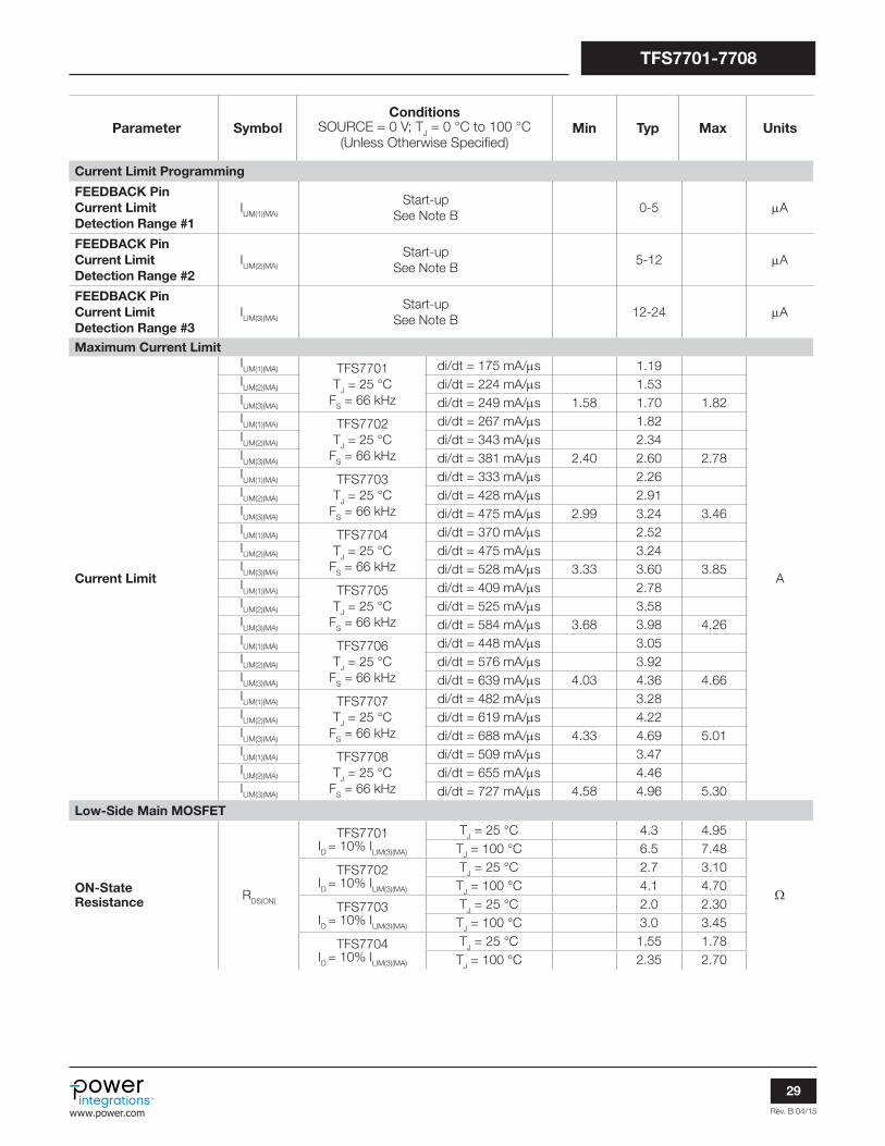
Rev. B 04/15
29
TFS7701-7708
www.power.com
Parameter SymbolConditions
SOURCE = 0 V; TJ = 0 °C to 100 °C (Unless Otherwise Specified)
Min Typ Max Units
Current Limit Programming
FEEDBACK Pin Current Limit Detection Range #1
ILIM(1)(MA)
Start-upSee Note B
0-5 mA
FEEDBACK Pin Current Limit Detection Range #2
ILIM(2)(MA)
Start-upSee Note B
5-12 mA
FEEDBACK Pin Current Limit Detection Range #3
ILIM(3)(MA)
Start-upSee Note B
12-24 mA
Maximum Current Limit
Current Limit
ILIM(1)(MA) TFS7701TJ = 25 °C
FS = 66 kHz
di/dt = 175 mA/ms 1.19
A
ILIM(2)(MA) di/dt = 224 mA/ms 1.53ILIM(3)(MA) di/dt = 249 mA/ms 1.58 1.70 1.82ILIM(1)(MA) TFS7702
TJ = 25 °CFS = 66 kHz
di/dt = 267 mA/ms 1.82ILIM(2)(MA) di/dt = 343 mA/ms 2.34ILIM(3)(MA) di/dt = 381 mA/ms 2.40 2.60 2.78ILIM(1)(MA) TFS7703
TJ = 25 °CFS = 66 kHz
di/dt = 333 mA/ms 2.26ILIM(2)(MA) di/dt = 428 mA/ms 2.91ILIM(3)(MA) di/dt = 475 mA/ms 2.99 3.24 3.46ILIM(1)(MA) TFS7704
TJ = 25 °CFS = 66 kHz
di/dt = 370 mA/ms 2.52ILIM(2)(MA) di/dt = 475 mA/ms 3.24ILIM(3)(MA) di/dt = 528 mA/ms 3.33 3.60 3.85ILIM(1)(MA) TFS7705
TJ = 25 °CFS = 66 kHz
di/dt = 409 mA/ms 2.78ILIM(2)(MA) di/dt = 525 mA/ms 3.58ILIM(3)(MA) di/dt = 584 mA/ms 3.68 3.98 4.26ILIM(1)(MA) TFS7706
TJ = 25 °CFS = 66 kHz
di/dt = 448 mA/ms 3.05ILIM(2)(MA) di/dt = 576 mA/ms 3.92ILIM(3)(MA) di/dt = 639 mA/ms 4.03 4.36 4.66ILIM(1)(MA) TFS7707
TJ = 25 °CFS = 66 kHz
di/dt = 482 mA/ms 3.28ILIM(2)(MA) di/dt = 619 mA/ms 4.22ILIM(3)(MA) di/dt = 688 mA/ms 4.33 4.69 5.01ILIM(1)(MA) TFS7708
TJ = 25 °CFS = 66 kHz
di/dt = 509 mA/ms 3.47ILIM(2)(MA) di/dt = 655 mA/ms 4.46ILIM(3)(MA) di/dt = 727 mA/ms 4.58 4.96 5.30
Low-Side Main MOSFET
ON-StateResistance RDS(ON)
TFS7701ID = 10% ILIM(3)(MA)
TJ = 25 °C 4.3 4.95
W
TJ = 100 °C 6.5 7.48
TFS7702ID = 10% ILIM(3)(MA)
TJ = 25 °C 2.7 3.10TJ = 100 °C 4.1 4.70
TFS7703ID = 10% ILIM(3)(MA)
TJ = 25 °C 2.0 2.30TJ = 100 °C 3.0 3.45
TFS7704ID = 10% ILIM(3)(MA)
TJ = 25 °C 1.55 1.78TJ = 100 °C 2.35 2.70
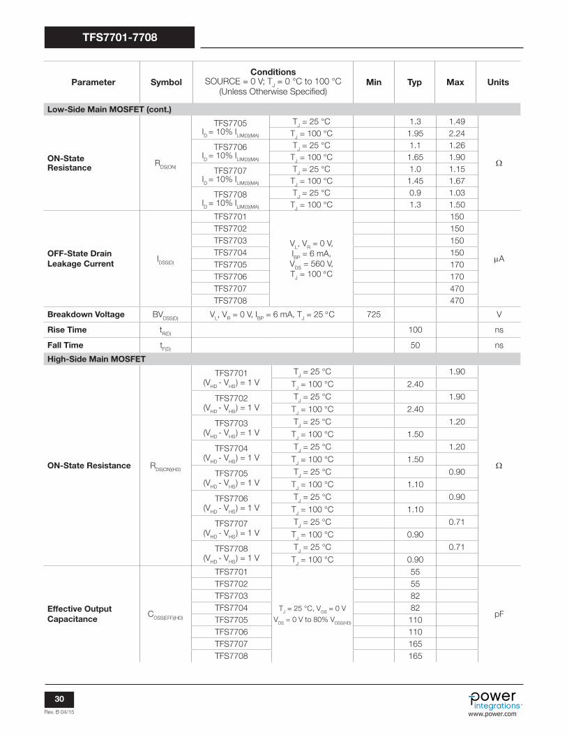
Rev. B 04/15
30
TFS7701-7708
www.power.com
Parameter SymbolConditions
SOURCE = 0 V; TJ = 0 °C to 100 °C (Unless Otherwise Specified)
Min Typ Max Units
Low-Side Main MOSFET (cont.)
ON-StateResistance RDS(ON)
TFS7705ID = 10% ILIM(3)(MA)
TJ = 25 °C 1.3 1.49
W
TJ = 100 °C 1.95 2.24
TFS7706ID = 10% ILIM(3)(MA)
TJ = 25 °C 1.1 1.26TJ = 100 °C 1.65 1.90
TFS7707ID = 10% ILIM(3)(MA)
TJ = 25 °C 1.0 1.15TJ = 100 °C 1.45 1.67
TFS7708ID = 10% ILIM(3)(MA)
TJ = 25 °C 0.9 1.03TJ = 100 °C 1.3 1.50
OFF-State Drain Leakage Current
IDSS(D)
TFS7701
VL, VR = 0 V, IBP = 6 mA, VDS = 560 V, TJ = 100 °C
150
mA
TFS7702 150TFS7703 150TFS7704 150TFS7705 170TFS7706 170TFS7707 470TFS7708 470
Breakdown Voltage BVDSS(D) VL, VR = 0 V, IBP = 6 mA, TJ = 25 °C 725 V
Rise Time tR(D) 100 ns
Fall Time tF(D) 50 ns
High-Side Main MOSFET
ON-State Resistance RDS(ON)(HD)
TFS7701(VHD - VHS) = 1 V
TJ = 25 °C 1.90
W
TJ = 100 °C 2.40
TFS7702(VHD - VHS) = 1 V
TJ = 25 °C 1.90
TJ = 100 °C 2.40
TFS7703(VHD - VHS) = 1 V
TJ = 25 °C 1.20
TJ = 100 °C 1.50
TFS7704(VHD - VHS) = 1 V
TJ = 25 °C 1.20
TJ = 100 °C 1.50
TFS7705(VHD - VHS) = 1 V
TJ = 25 °C 0.90
TJ = 100 °C 1.10
TFS7706(VHD - VHS) = 1 V
TJ = 25 °C 0.90
TJ = 100 °C 1.10
TFS7707(VHD - VHS) = 1 V
TJ = 25 °C 0.71
TJ = 100 °C 0.90
TFS7708(VHD - VHS) = 1 V
TJ = 25 °C 0.71
TJ = 100 °C 0.90
Effective Output Capacitance
COSS(EFF)(HD)
TFS7701
TJ = 25 °C, VGS = 0 V
VDS = 0 V to 80% VDSS(HD)
55
pF
TFS7702 55TFS7703 82TFS7704 82TFS7705 110TFS7706 110TFS7707 165TFS7708 165
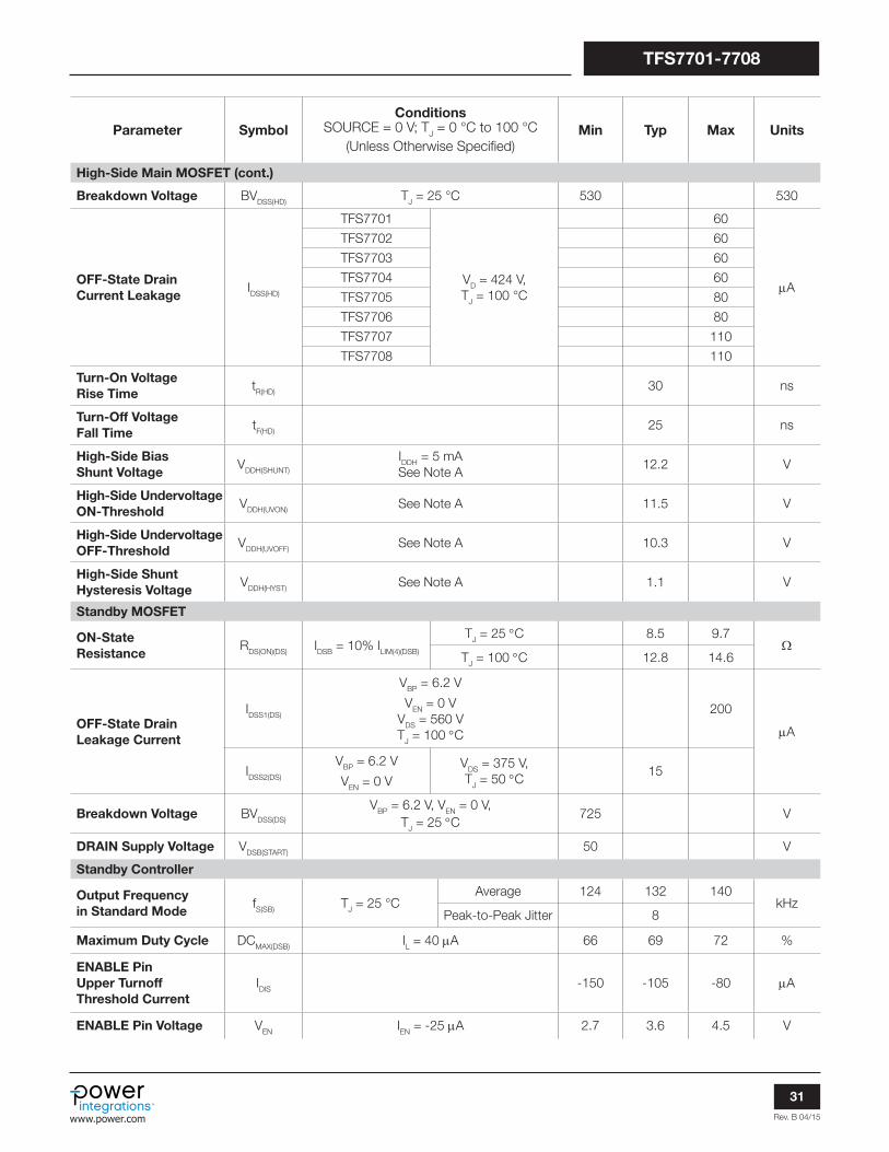
Rev. B 04/15
31
TFS7701-7708
www.power.com
Parameter SymbolConditions
SOURCE = 0 V; TJ = 0 °C to 100 °C (Unless Otherwise Specified)
Min Typ Max Units
High-Side Main MOSFET (cont.)
Breakdown Voltage BVDSS(HD) TJ = 25 °C 530 530
OFF-State Drain Current Leakage
IDSS(HD)
TFS7701
VD = 424 V,TJ = 100 °C
60
mA
TFS7702 60
TFS7703 60
TFS7704 60
TFS7705 80
TFS7706 80
TFS7707 110
TFS7708 110
Turn-On Voltage Rise Time
tR(HD) 30 ns
Turn-Off Voltage Fall Time
tF(HD) 25 ns
High-Side Bias Shunt Voltage
VDDH(SHUNT)
IDDH = 5 mA See Note A
12.2 V
High-Side Undervoltage ON-Threshold
VDDH(UVON) See Note A 11.5 V
High-Side Undervoltage OFF-Threshold
VDDH(UVOFF) See Note A 10.3 V
High-Side Shunt Hysteresis Voltage
VDDH(HYST) See Note A 1.1 V
Standby MOSFET
ON-State Resistance
RDS(ON)(DS) IDSB = 10% ILIM(4)(DSB)
TJ = 25 °C 8.5 9.7W
TJ = 100 °C 12.8 14.6
OFF-State Drain Leakage Current
IDSS1(DS)
VBP = 6.2 V
VEN = 0 V VDS = 560 V TJ = 100 °C
200
mA
IDSS2(DS)
VBP = 6.2 V
VEN = 0 VVDS = 375 V, TJ = 50 °C 15
Breakdown Voltage BVDSS(DS)
VBP = 6.2 V, VEN = 0 V, TJ = 25 °C
725 V
DRAIN Supply Voltage VDSB(START) 50 V
Standby Controller
Output Frequency in Standard Mode
fS(SB) TJ = 25 °CAverage 124 132 140
kHzPeak-to-Peak Jitter 8
Maximum Duty Cycle DCMAX(DSB) IL = 40 mA 66 69 72 %
ENABLE Pin Upper Turnoff Threshold Current
IDIS -150 -105 -80 mA
ENABLE Pin Voltage VEN IEN = -25 mA 2.7 3.6 4.5 V

Rev. B 04/15
32
TFS7701-7708
www.power.com
Parameter SymbolConditions
SOURCE = 0 V; TJ = 0 °C to 100 °C (Unless Otherwise Specified)
Min Typ Max Units
Standby Controller (cont.)
BYPASS Pin Charge Current
ICH1
VBP = 0 V,TJ = 25 °C
-5 -4.0 -2
mA
ICH2
VBP = 4 V,TJ = 25 °C
-4 -2.1 0
BYPASS Pin Voltage VBP VDS = 50 V 5.60 5.80 6.00 V
BYPASS Pin Voltage Hysteresis
VBP(HYST) 0.80 1.1 1.3 V
BYPASS Pin Shunt Voltage
VBP(SHUNT) IBP = 2 mA 5.8 6.15 6.4 V
Standby Circuit Protection
ENABLE Pin Current Limit Selection Range #1
ILIM(1)(DSB) Start-up 0-5 mA
ENABLE Pin Current Limit Selection Range #2
ILIM(2)(DSB) Start-up 5-12 mA
ENABLE Pin Current Limit Selection Range #3
ILIM(3)(DSB) Start-up 12-24 mA
ENABLE Pin Current Limit Selection Range #4
ILIM(4)(DSB) Start-up 24-48 mA
Standby Current Limit
ILIM(1)(DSB) IL = 20 mA, di/dt = 95 mA/ms, TJ = 25 °C 450 500 540
mAILIM(2)(DSB) IL = 20 mA, di/dt = 105 mA/ms, TJ = 25 °C 500 550 600
ILIM(3)(DSB) IL = 20 mA, di/dt = 123 mA/ms, TJ = 25 °C 610 650 690
ILIM(4)(DSB) IL = 20 mA, di/dt = 143 mA/ms, TJ = 25 °C 690 750 810
Δ ILIM
ILIM (IL = 100 mA) / ILIM (IL = 20 mA)di/dt = 125 mA/ms
84 %
General Circuit Protection
Power Coefficient I2fI2f = ILIM(3)(DSB)(TYP)× fS(SB)(OSC)(TYP)
TJ = 25 °C0.9 × I2f I2f 1.12 × I2f A2Hz
Initial Current Limit IINIT
TJ = 25 °CSee Note D
0.75 × ILIM(MIN)
Leading Edge Blanking Time (Main)
tLEB(D) TJ = 25 °C 150 ns
Leading Edge Blanking Time (Standby)
tLEB(DSB)
TJ = 25 °CSee Note D
170 215 ns
Current Limit Delay (Main)
tILD(D) TJ = 25 °C 150 ns

Rev. B 04/15
33
TFS7701-7708
www.power.com
Parameter SymbolConditions
SOURCE = 0 V; TJ = 0 °C to 100 °C (Unless Otherwise Specified)
Min Typ Max Units
General Circuit Protection (cont.)
Current Limit Delay (Standby)
tILD(DSB) TJ = 25 °C 150 ns
Thermal Shutdown Temperature
TSD See Note D 118 °C
Thermal Shutdown Hysteresis
TSD(HYST) 55 °C
Auto-Restart ON-Time at fOSC Standby
tAR TJ = 25 °C 64 ms
Auto-Restart Duty Cycle Standby
DCAR TJ = 25 °C 2.2 %
Supply Current
DRAIN Supply Current
IS1
EN Current > IDIS (No MOSFETs Switching)
200 550 800
mA
IS2
EN Open (Standby MOSFET Switching at fOSC)
360 710 960
NOTES:A. VDDH(SHUNT) minus VDDH(UV_ON) is equal to 250 mV minimum.B. Level 1 RFB = open, Level 2 RFB = 511 kW, Level 3 RFB = 232 kW.C. Level 1 REN = open, Level 2 REN = 511 kW, Level 3 REN = 232 kW, Level 4 REN = 107 kW.D. Guaranteed by characterization. Not tested in production.

Rev. B 04/15
34
TFS7701-7708
www.power.com
Typical Performance CharacteristicsNote: Curves shown with fS1(MA) = 66 kHz and fS(SB) = 132 kHz.
Figure 32. Main Supply. Breakdown Voltage vs. Temperature. Figure 33. Standby Supply. Breakdown vs. Temperature.
Figure 34. Main Switching Frequency vs. Temperature.
Figure 35. Standby Switching Frequency vs. Temperature.
Figure 36. Main Drain (D) Current Limit vs. Temperature. Figure 37. Standby Drain (DSB) Current Limit vs. Temperature.
1.2
1.0
0.8
0.6
0.4
0.2
0.0-50 -25 0 25 50 75 100 125
Junction Temperature (°C)
PI-
7055
-061
713
MA
IN D
RA
IN (D
) Cu
rren
t L
imit
(No
rmal
ized
to
25 °C
)
1.2
1.0
0.8
0.6
0.4
0.2
0.0-50 -25 0 25 50 75 100 125
Junction Temperature (°C)
PI-
7053
-061
713
MA
IN D
RA
IN (D
) Ou
tpu
t F
req
uen
cy(N
orm
aliz
ed t
o 2
5 °C
)
1.2
1.0
0.8
0.6
0.4
0.2
0.0-50 -25 0 25 50 75 100 125
Junction Temperature (°C)
PI-
7054
-061
713
STA
ND
BY
DR
AIN
(DS
B) O
utp
ut
Fre
qu
ency
(No
rmal
ized
to
25 °C
)
1.2
1.0
0.8
0.6
0.4
0.2
0.0-50 -25 0 25 50 75 100 125
Junction Temperature (°C)
PI-
7056
-061
713
STA
ND
BY
DR
AIN
(DS
B) C
urr
ent
Lim
it(N
orm
aliz
ed t
o 2
5 °C
)
1.1
1.0
0.9-50 -25 0 25 50 75 100 125 150
Junction Temperature (°C)
MA
IN D
RA
IN P
in B
reak
do
wn
Volt
age
(No
rmal
ized
to
25 °C
) PI-
5998
-060
210 1.1
1.0
0.9-50 -25 0 25 50 75 100 125 150
Junction Temperature (°C)
STA
ND
BY
DR
AIN
Pin
Bre
akd
ow
n Vo
ltag
e(N
orm
aliz
ed t
o 2
5 °C
) PI-
5999
-060
210

Rev. B 04/15
35
TFS7701-7708
www.power.com
Typical Performance Characteristics (cont.)
Figure 39. LINE-SENSE (L) Pin Voltage vs. Current.
Figure 40. RESET (R) Pin Voltage vs. Current. Figure 41. FEEDBACK (FB) Pin Current vs. Voltage.
Figure 42. ENABLE (EN) Pin Current vs. Voltage. Figure 43. BYPASS (BP) Pin Current vs. Voltage.
Figure 38. Standby Supply. Undervoltage Threshold vs. Junction Temperature.
1.2
1.0
0.8
0.6
0.4
0.2
0.0-50 -25 0 25 50 75 100 125
Junction Temperature (°C)P
I-70
57-0
6171
3
LIN
E-S
EN
SE
Pin
Sta
nd
by
Un
der
volt
age
(No
rmal
ized
to
25 °C
)4
3
2
1
00 20 40 60 80 100 120 140 160
LINE-SENSE Pin Current (µA)
PI-
7058
-061
313
LIN
E-S
EN
SE
Pin
Vo
ltag
e (V
)
5
4
2
3
1
00 50 100 150 200 250
RESET Pin Current (µA)
PI-
7059
-061
313
RE
SE
T P
in V
olt
age
(V)
1
0
-3
-2
-1
-4
-50 1 2 3 4 5 6 7
FEEDBACK Pin Voltage (V)
PI-
7060
-061
313
FE
ED
BA
CK
Pin
Cu
rren
t (m
A)
150
100
-50
0
50
-100
-1500 1 2 3 4 5 6 7
ENABLE Pin Voltage (V)
PI-
7061
-061
313
EN
AB
LE
Pin
Cu
rren
t (µ
A)
25
20
10
15
5
00 2 4 6 8
BYPASS Pin Voltage (V)
PI-
7062
-061
713
BY
PA
SS
Pin
Cu
rren
t (m
A)

Rev. B 04/15
36
TFS7701-7708
www.power.com
Typical Performance Characteristics (cont.)
Figure 44. VDDH Pin Current vs. Voltage.
Figure 46. Duty Cycle vs. Temperature (IL = 115 mA, IR = 170 mA)
Figure 48. Drain Supply. Output Characteristics.
Figure 45. Duty Cycle vs. Temperature (IL = 100 mA, IR = 110 mA).
Figure 47. Standby Supply. Output Characteristics.
Figure 49. Standby Drain Capacitance vs. Drain Voltage.
00 2 4 6 8 10 12 14 16 18 20
STANDBY DRAIN Voltage (V)
DR
AIN
Cur
rent
(A) P
I-70
66-0
6171
3
0.5
0.75
0.25
TCASE = 25 °CTCASE = 100 °C
1
1.25
5
00 2 4 6 8 10 12 14 16 18 20
DRAIN Voltage (V)
DR
AIN
Cur
rent
(A) P
I-70
67-0
6171
3
2
1TCASE = 25 °CTCASE = 100 °C
4
3
TFS7701 0.34TFS7702 0.56TFS7703 0.76TFS7704 0.96TFS7705 1.16TFS7706 1.37TFS7707 1.57TFS7708 1.77
Scaling Factors:
0 100 200 300 400 500 6000
10
100
1000
PI-
7068
-061
413
STANDBY DRAIN (DBS) Pin Voltage (V)
STA
ND
BY
DR
AIN
(DS
B)
Cap
acit
ance
(pF)
50
40
20
30
10
00 4 8 12 16
VDDH Voltage (V)
PI-
7063
-061
713
VD
DH
Cu
rren
t (m
A)
1.2
1.0
0.8
0.6
0.4
0.2
0.0-50 -25 0 25 50 75 100 125
Junction Temperature (°C)
PI-
7064
-061
713
No
rmal
ized
Du
ty C
ycle
1.2
1.0
0.8
0.6
0.4
0.2
0.0-50 -25 0 25 50 75 100 125
Junction Temperature (°C)
PI-
7065
-061
713
No
rmal
ized
Du
ty C
ycle

Rev. B 04/15
37
TFS7701-7708
www.power.com
Typical Performance Characteristics (cont.)
Figure 50. Main Drain Capacitance vs. Drain Voltage. Figure 51. Standby Drain Switching Power vs. Drain Voltage.
Figure 52. Main Drain Switching Power vs. Drain Voltage. Figure 53. High-Side MOSFET (HD-HS) Drain Current vs. Drain Voltage.
Figure 54. High-Side MOSFET (HD-HS) Drain Current vs. Drain Voltage.
Figure 55. High-Side MOSFET Breakdown Voltage vs. Temperature.
1.1
1.0
0.9-50 -25 0 25 50 75 100 125 150
Temperature (°C)
Bre
akd
ow
n V
olt
age
(No
rmal
ized
to
25
°C) PI-
5972
-051
210
0 100 200 300 400 500 60010
100
1000
10000
PI-
7069
-061
413
MAIN DRAIN (D) Pin Voltage (V)
MA
IN D
RA
IN (D
) Cap
acit
ance
(pF)
TFS7701 0.34TFS7702 0.56TFS7703 0.76TFS7704 0.96TFS7705 1.16TFS7706 1.37TFS7707 1.57TFS7708 1.77
Scaling Factors:100
75
25
50
00 200100 400 500 600300
STANDBY DRAIN (DSB) Pin Voltage (V)
Po
wer
(mW
)
PI-
5946
-061
713
500
400
200
100
300
00 200100 400 500 600300 700
Po
wer
(mW
)
PI-
7071
-061
413
MAIN DRAIN (D) Pin Voltage (V)
TFS7701 0.34TFS7702 0.56TFS7703 0.76TFS7704 0.96TFS7705 1.16TFS7706 1.37TFS7708 1.57TFS7709 1.77
Scaling Factors:
20
0
0 1 2 3 4 5 6 7
HD-HS Voltage (V)
HD
-HS
Cur
rent
(A) P
I-77
02-0
6171
3
5
15
10
25 °C100 °C
TJ = 25 °CTJ = 100 °C
TFS7701 0.17TFS7702 0.17TFS7703 0.25TFS7704 0.25TFS7705 0.33TFS7706 0.33TFS7708 0.42TFS7709 0.42
Scaling Factors:
0 100 200 300 400100
1000
PI-
7073
-061
713
CO
SS (p
F)
TFS7701 0.17TFS7702 0.17TFS7703 0.25TFS7704 0.25TFS7705 0.33TFS7706 0.33TFS7708 0.42TFS7709 0.42
Scaling Factors:
HD-HS Voltage (V)
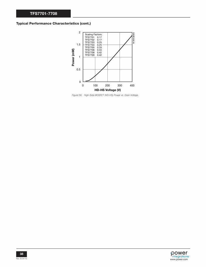
Rev. B 04/15
38
TFS7701-7708
www.power.com
Typical Performance Characteristics (cont.)
Figure 56. High-Side MOSFET (HD-HS) Power vs. Drain Voltage.
2
1.5
1
0.5
00 100 200 300 400
Po
wer
(mW
)
PI-
7074
-061
813
HD-HS Voltage (V)
TFS7701 0.17TFS7702 0.17TFS7703 0.25TFS7704 0.25TFS7705 0.33TFS7706 0.33TFS7708 0.42TFS7709 0.42
Scaling Factors:

Rev. B 04/15
39
TFS7701-7708
www.power.com
Figure 57. Heat Sink Assembly – using Thermally Conductive Silicone Grease.
TFS2CLIP
SELF TAP SCREW
THERMALGREASE

Rev. B 04/15
40
TFS7701-7708
www.power.com
PI-
7080
-070
813
No
tes:
1. D
imen
sio
ning
and
to
lera
ncin
g p
er A
SM
E Y
14.5
M-1
994.
2. D
imen
sio
ns n
ote
d a
re d
eter
min
ed a
t th
e o
uter
mo
st e
xtre
mes
of
the
pla
stic
bo
dy
excl
usiv
e o
f
mo
ld fl
ash,
tie
bar
bur
rs, g
ate
bur
rs, a
nd in
terl
ead
flas
h, b
ut in
clud
ing
any
mis
mat
ch b
etw
een
t
he t
op
and
bo
tto
m o
f th
e p
last
ic b
od
y. M
axim
um m
old
pro
trus
ion
is 0
.007
[0.
18]
per
sid
e.
3. D
imen
sio
ns n
ote
d a
re in
clus
ive
of
pla
ting
thi
ckne
ss.
4. D
oes
no
t in
clud
e in
terl
ead
flas
h o
r p
rotr
usio
ns.
5. C
ont
rolli
ng d
imen
sio
ns in
inch
es (m
m).
6.
7.
Tie
d t
o S
OU
RC
E (P
in 6
).
8. T
ied
to
HS
(Pin
14)
.
9.
10. T
ied
to
HD
(Pin
16)
.
0.62
8 (1
5.95
) Ref
.
0.01
9 (0
.48)
Ref
.
0.06
0 (1
.52)
Ref
.10
° R
ef.
All
Aro
und
0.02
1 (0
.53)
0.01
9 (0
.48)
0.04
8 (1
.22)
0.04
6 (1
.17)
0.02
7 (0
.70)
0.02
3 (0
.58)
0.02
0 (0
.50)
0.01
6 (0
.41)
Ref
.
Det
ail A
Pin
1
0.11
8 (3
.00)
0.14
0 (3
.56)
0.12
0 (3
.05)0.08
1 (2
.06)
0.07
7 (1
.96)
13×
0.01
6 (0
.41)
0.01
1 (0
.28)
0.02
0 M
0.5
1 M
C
3
10
67
8
9
0.29
0 (7
.37)
Ref
.
0.04
7 (1
.19)
C
0.03
8 (0
.97)
0.05
6 (1
.42)
Ref
.
0.01
2 (0
.30)
Typ
.
0.10
1 (2
.57)
Ref
.
0.16
7 (4
.24)
Ref
.
0.23
5 (5
.96)
Ref
.
0.03
5 (0
.89)
Ref
.
0.01
0 (0
.25)
Typ
.
0.04
1 (1
.04)
Ref
.
0.02
0 (0
.51)
Ref
.
13
56
78
910
1113
1416
0.65
3 (1
6.59
)0.
647
(16.
43)
2
0.32
5 (8
.25)
0.32
0 (8
.13)2
A
B
Pin
1 I.
D.
0.38
1 (9
.68)
Ref
.
0.07
6 (1
.93) 0.
012
(0.3
0) R
ef.
0.20
1 (5
.11)
Ref
.
0.20
7 (5
.26)
0.18
7 (4
.75)
13×
0.02
4 (0
.61)
0.01
9 (0
.48)
0.01
0 M
0.2
5 M
C A
B
43
0.51
9 (1
3.18
)R
ef.
FRO
NT
VIE
WS
IDE
VIE
WB
AC
K V
IEW
Det
ail A
(Sca
le =
9×)
EN
D V
IEW
eSIP
-16F
(H P
acka
ge)
MO
UN
TIN
G H
OL
E P
AT
TE
RN
(N
.T.S
)A
ll d
imen
sio
ns
in in
ches
(m
m)
0.15
2(3
.88)
51
6
0.11
4(2
.91)
79
1114
0.11
4(2
.91)
0.11
4(2
.91)
0.07
6(1
.94)
0.07
6(1
.94)
0.07
6(1
.94)
0.11
4(2
.91)
38
1016
13
TOP
EN
D V
IEW
B-B
Lo
cati
on
of
exp
ose
d m
etal
tie
-bar
s

Rev. B 04/15
41
TFS7701-7708
www.power.com
Part Marking Information
• HiperTFS-2 Product Family
• TFS Series Number
• Package Identifier
H Plastic eSIP-16F. Halogen Free and RoHS Compliant TFS 7705 H
Part Ordering Information
Part Number Option Quantity
TFS7701H Tube 30
TFS7702H Tube 30
TFS7703H Tube 30
TFS7704H Tube 30
TFS7705H Tube 30
TFS7706H Tube 30
TFS7707H Tube 30
TFS7708H Tube 30

Revision Notes Date
A Code A. 11/13
B Moved location of “output short-circuit protection (SCP)” bullet point on page 3. 04/15
For the latest updates, visit our website: www.power.comPower Integrations reserves the right to make changes to its products at any time to improve reliability or manufacturability. Power Integrations does not assume any liability arising from the use of any device or circuit described herein. POWER INTEGRATIONS MAKES NO WARRANTY HEREIN AND SPECIFICALLY DISCLAIMS ALL WARRANTIES INCLUDING, WITHOUT LIMITATION, THE IMPLIED WARRANTIES OF MERCHANTABILITY, FITNESS FOR A PARTICULAR PURPOSE, AND NON-INFRINGEMENT OF THIRD PARTY RIGHTS.
Patent InformationThe products and applications illustrated herein (including transformer construction and circuits external to the products) may be covered by one or more U.S. and foreign patents, or potentially by pending U.S. and foreign patent applications assigned to Power Integrations. A complete list of Power Integrations patents may be found at www.power.com. Power Integrations grants its customers a license under certain patent rights as set forth at http://www.power.com/ip.htm.
Life Support PolicyPOWER INTEGRATIONS PRODUCTS ARE NOT AUTHORIZED FOR USE AS CRITICAL COMPONENTS IN LIFE SUPPORT DEVICES OR SYSTEMS WITHOUT THE EXPRESS WRITTEN APPROVAL OF THE PRESIDENT OF POWER INTEGRATIONS. As used herein:
1. A Life support device or system is one which, (i) is intended for surgical implant into the body, or (ii) supports or sustains life, and (iii) whose failure to perform, when properly used in accordance with instructions for use, can be reasonably expected to result in significant injury or death to the user.
2. A critical component is any component of a life support device or system whose failure to perform can be reasonably expected to cause the failure of the life support device or system, or to affect its safety or effectiveness.
The PI logo, TOPSwitch, TinySwitch, LinkSwitch, LYTSwitch, InnoSwitch, DPA-Switch, PeakSwitch, CAPZero, SENZero, LinkZero, HiperPFS, HiperTFS, HiperLCS, Qspeed, EcoSmart, Clampless, E-Shield, Filterfuse, FluxLink, StakFET, PI Expert and PI FACTS are trademarks of Power Integrations, Inc. Other trademarks are property of their respective companies. ©2014, Power Integrations, Inc.
Power Integrations Worldwide Sales Support Locations
World Headquarters5245 Hellyer AvenueSan Jose, CA 95138, USA.Main: +1-408-414-9200Customer Service:Phone: +1-408-414-9665Fax: +1-408-414-9765e-mail: [email protected]
China (Shanghai)Rm 1601/1610, Tower 1,Kerry Everbright CityNo. 218 Tianmu Road West,Shanghai, P.R.C. 200070Phone: +86-21-6354-6323Fax: +86-21-6354-6325e-mail: [email protected]
China (Shenzhen)17/F, Hivac Building, No. 2,Keji Nan 8th Road, Nanshan District, Shenzhen, China, 518057Phone: +86-755-8672-8689Fax: +86-755-8672-8690e-mail: [email protected]
GermanyLindwurmstrasse 11480337 MunichGermanyPhone: +49-895-527-39110Fax: +49-895-527-39200e-mail: [email protected]
India#1, 14th Main RoadVasanthanagarBangalore-560052 IndiaPhone: +91-80-4113-8020Fax: +91-80-4113-8023e-mail: [email protected]
ItalyVia Milanese 20, 3rd. Fl.20099 Sesto San Giovanni (MI)ItalyPhone: +39-024-550-8701Fax: +39-028-928-6009e-mail: [email protected]
JapanKosei Dai-3 Bldg. 2-12-11, Shin-Yokohama, Kohoku-ku Yokohama-shi Kanagwan 222-0033 JapanPhone: +81-45-471-1021Fax: +81-45-471-3717e-mail: [email protected]
KoreaRM 602, 6FLKorea City Air Terminal B/D, 159-6Samsung-Dong, Kangnam-Gu,Seoul, 135-728, KoreaPhone: +82-2-2016-6610Fax: +82-2-2016-6630e-mail: [email protected]
Singapore51 Newton Road#19-01/05 Goldhill PlazaSingapore, 308900Phone: +65-6358-2160Fax: +65-6358-2015e-mail: [email protected]
Taiwan5F, No. 318, Nei Hu Rd., Sec. 1Nei Hu Dist.Taipei 11493, Taiwan R.O.C.Phone: +886-2-2659-4570Fax: +886-2-2659-4550e-mail: [email protected]
UKFirst Floor, Unit 15, MeadwayCourt, Rutherford Close,Stevenage, Herts. SG1 2EFUnited KingdomPhone: +44 (0) 1252-730-141Fax: +44 (0) 1252-727-689e-mail: [email protected]