
TETRIS002
34
IMEC’S TECHNOLOGY TARGETING SERVICE A TECHNICAL OVERVIEW
-
Upload
imectechnologytargeting -
Category
Technology
-
view
768 -
download
0
Transcript of TETRIS002

IMEC’S TECHNOLOGY TARGETING SERVICE
A TECHNICAL OVERVIEW

HOW TO USE THIS DOCUMENT
2
This document illustrates how imec’s Technology Targeting Service can provide aquantitative analysis of different foundry technologies. Imec’s approach is to compare theperformance, power and area of selected IP blocks implemented in two or more targettechnology and/or design options.
For the purpose illustrating our procedures, two broadly similar TSMC technologies at the90nm and 65nm nodes have been selected. This straightforward node comparison permitsa simplified analysis suitable for an introduction to imec’s Technology Targeting Service.
The procedures are, however, are not restricted to assessing the port of a design fromone technology node to its equivalent scaled successor.

EXAMPLES OF OTHER TARGETING
REQUESTS
3
Examples of other requested comparisons include:
• Comparison of 40nm low power (LP), low threshold voltage (LVT) IP-blockperformance versus 40nm high performance (G) standard threshold voltage(SVT) IP-block performance.
• Comparison of 65nm low power, standard threshold voltage IP-blockperformance at nominal supply voltage versus 40nm high performance, standardthreshold voltage IP-block performance at 20% reduced supply voltage.
• Comparison of 65nm low power, standard threshold voltage IP-blockimplemented using 9-track and 12-track standard cell libraries.

1. INTRODUCTION
4
In this document, a relatively small gate-count, open-source Digital Signal Processor(DSP) has been selected. This processor is characterized by a relatively large logicdepth whose functionality makes extensive use of full-adder standard cells withrelatively short communication paths. It is also possible to select other circuits withdifferent characteristics from of a library which currently contains over 30 IP-blocks.
Larger gate counts will impose a different balance between gate and wire delays, andsmaller logic depths place more emphasis on the delay and set-up times of flip-flops.One of the reasons for selecting a relatively small gate DSP is that it enables the trade-off between area and clock rate to be explored over a wide range of target clock rates.Customers may also elect to provide their own IP for analysis.

5
Section 2 will begin by providing an overview of the selected process options atthe level of the device and interconnect.
In order to ensure accurate cell-level and IP-block level analysis, the values forthese parameters obtained from the relevant Design Rule Manuals (DRM’s) arecompared with values extracted from Spectre simulations using the foundrydevice models employed for library characterization.
Section 3 summarizes the key properties of the selected libraries and performsan analysis of the delay, static power and area at the level of individual cells.
The performance, dynamic and static power and area of the selected IP-blocksynthesized using the two selected technology options is analysed in Section 4.These metrics are then interpreted in terms of the device-level and cell-leveldata provided in the previous sections.
The report ends with a summary of the results in Section 5.
1. INTRODUCTION

2. DEVICE LEVEL ANALYSISReality check
6
We begin with a reality check.
Data extracted from the most the recentTSMC Design Rule Manuals (DRM’s) arecompared with data extracted fromdirect SPICE simulation using the mostrecent device model (shown inparentheses).
In the analysis that follows, we shall usethe 90nm node as the reference nodeand refer any changes in parametersrelative to this node.
The most notable feature is the absence of any reduction in nominal supply voltage which willinevitably result in a reduction in potential dynamic power savings. There is, however, a veryimpressive 50% increase in drive current per micron of gate width for the PMOS devices and asmaller but still significant increase of 14% for the NMOS devices. This improvement in driveper unit gate width has, of course, to be offset by the reduction in the maximum gate width(approximately 70%) that can be accommodated within a reduced 65nm standard cell height.
Technology Option CLN90 LP SVT CLN65 LP SVT
Design rule manual T-N90-LO-DR-001, v2.2 (11-12-09) T-N65-CL-DR-001, v2.0 (10-27-09)
Device model version CRN90LP_2d5_lk_v1d2p1 (03-14-09) CLN65LP_2d5_lk_v1d3 (05-11-09)
Front-end Features
NMOS PMOS NMOS PMOS
Vdd, Nominal supply voltage (V) 1.2 1.2
Lmin, Minimum gate length Lmin (um) 0.1 0.06
Vt_lin, Linear Vt at Vd=50mV (V) 0.417 (0.534) 0.439 (0.457) 0.402 (0.549) 0.475 (0.572)
Vt_sat, Saturation Vt at Vd=Vdd (V) 0.333 (0.351) 0.340 (0.285) 0.296 (0.336) 0.356 (0.371)
DIBL (V) 0.084 (0.054) -0.099 (-0.172) 0.106 (0.173) -0.119 (-0.179)
Id_sat (uA/um) 530 (537) 215 (219) 603 (602) 317 (315)
Ioff (pA/um) 300 (246) 236 (230) 211 (315) 129 (146)
Body effect ∆Vt_sat at Vb = |Vdd/2| (V) 0.077 (0.052) 0.089 (0.054) 0.043 (0.033) 0.060 (0.063)
Coverlay (fF/um) 0.268 0.224 0.221 0.214
Cjunction (fF/um2) 0.981 1.09 1.251 1.077
RO delay Inverter FO=1 (ps/gate) 12.76 9.331
Back-end features
Number of metal layers 3-9 3-9
M1 width/space(um) 0.12/0.12 0.09/0.09
MX width/space (um) 0.14/0.14 0.10/0.10
MY width/space (um) 0.28/0.28 0.20/0.20
MN width/space (um) 0.42/0.42 0.40/0.40
M1 Ctotal, M2-M1-FOX (fF/um) 0.250 0.239
MX Ctotal, M3-M2-M1 (fF/um) 0.233 0.221
Table 1

7
These improvements in device performance have been paid for by a decrease inchannel control as measured by the Drain Induced Barrier Lowering (DIBL)parameter. For ideal, well controlled devices, the threshold voltage should not bedependent on the source-drain voltage, Vds. As geometry scaling moves thedepletion layers surrounding the source and drain regions closer together theyincrease their interaction and the threshold voltage decreases as an increasing Vds
increases the size of the depletion regions.
For both processes the linear threshold voltage is measured at a standard valueof Vds=50mV, while the saturation threshold voltage is measured at Vds=1.2V. Thedifference between the linear and saturation threshold voltages defines the DIBLparameter in volts. We see that the transition to 65nm results in an increase inDIBL of approximately 20%. Poor channel control, and corresponding high DIBLvalues, directly impact performance because it results in an increase in theeffective output switching resistance of the device.
The body effect measures the change in threshold voltage as the voltage appliedbetween the source and the substrate is changed from zero to -Vdd/2 (for anNMOS device). We observe the continuing trend of a reduction in the body effectat the 65nm node.
2. DEVICE LEVEL ANALYSISDiscussion

8
A commonly used figure of merit use to characterize device performance is theintrinsic device switching time τi defined by
where Cg is the total gate capacitance per um of gate width, Vdd is the supplyvoltage and Id_sat is the drive current per um of gate width for Vds=Vdd, Vgs=Vdd.
Although approximate, the advantage of this figure of merit for processtechnologists is that the resulting switching time is independent of gate width,since the width variation of the gate capacitance in the numerator is cancelledby a corresponding variation in gate drive current in the denominator.
During a logic switching transition, the rise time of the gate is largelycontrolled by the ability of the PMOS device to source current from the positivepower rail to the load, while the fall time of the gate is dominated by theability of the NMOS device to sink current from the load to ground. The sumof the intrinsic switch times for the NMOS and PMOS devices thereforerepresents an approximate and gate width independent measure of intrinsicinverter performance
satd
ddgi
I
VC
_
pmos
i
nmos
iinv
2. DEVICE LEVEL ANALYSISMetrics

9
From the data in Table 1, the following values for the intrinsic inverter switchingtime are calculated
These are compared with the data in Table 1 for the Ring Oscillator delay perinverter state:
which correspond to a 27% improvement in inverter Ring Oscillator delay perinverter stage and therefore confirms the usefulness (for 90nm and 65nm nodes)of relative performance estimation based on the intrinsic switching time.
The next five pages show the SPICE data from the device models used to extractthe device parameters of Table 1.
ps331.9ps 76.12 65nm
RO
90 nm
RO
ps9.1ps 7.2 65nm
inv
90 nm
inv
2. DEVICE LEVEL ANALYSISMetric comparison
10
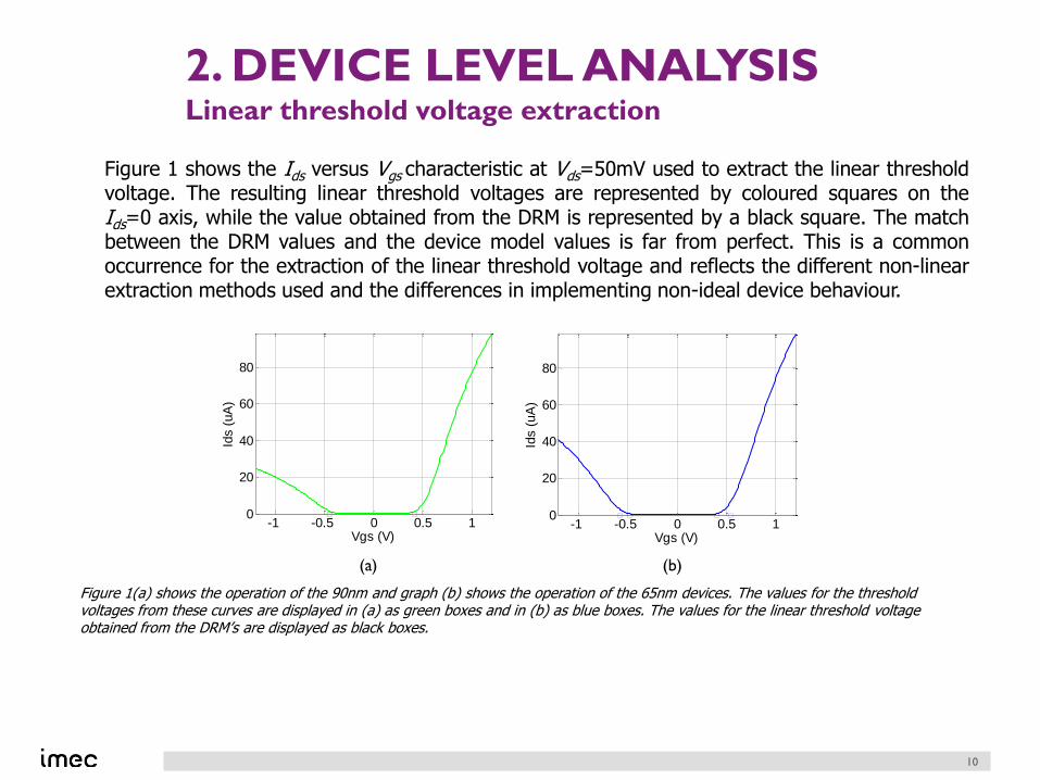
Figure 1 shows the Ids versus Vgs characteristic at Vds=50mV used to extract the linear thresholdvoltage. The resulting linear threshold voltages are represented by coloured squares on theIds=0 axis, while the value obtained from the DRM is represented by a black square. The matchbetween the DRM values and the device model values is far from perfect. This is a commonoccurrence for the extraction of the linear threshold voltage and reflects the different non-linearextraction methods used and the differences in implementing non-ideal device behaviour.
-1 -0.5 0 0.5 10
20
40
60
80
Vgs (V)
Ids (
uA
)
-1 -0.5 0 0.5 10
20
40
60
80
Vgs (V)Id
s (
uA
)
(a) (b)
Figure 1(a) shows the operation of the 90nm and graph (b) shows the operation of the 65nm devices. The values for the threshold voltages from these curves are displayed in (a) as green boxes and in (b) as blue boxes. The values for the linear threshold voltage obtained from the DRM’s are displayed as black boxes.
2. DEVICE LEVEL ANALYSISLinear threshold voltage extraction

11
Figure 2 shows the Ids versus Vgs characteristic at Vds=1.2V used to extract the saturation threshold voltage. The resulting saturation threshold voltages are represented by colouredsquares on the Ids=0 axis, while the value obtained from the DRM is represented by a black square. While not perfect, the matches between the DRM and device model values are better than for the linear regime.
-1 -0.5 0 0.5 10
100
200
300
400
500
Vgs (V)
Ids (
uA
)
-1 -0.5 0 0.5 10
100
200
300
400
500
600
Vgs (V)
Ids (
uA
)
(a) (b)
Figure 2(a) shows the operation of the 90nm and graph (b) shows the operation of the 65nm device. The values for the threshold voltages from these curves are displayed in (a) as green boxes and in (b) as blue boxes. The values for the saturation threshold voltages obtained from the DRM’s are displayed as black boxes.
2. DEVICE LEVEL ANALYSISSaturation threshold voltage extraction

12
Figure 3 shows the Ids versus Vds characteristic at Vgs=1.2V used to extract the value of Id_sat
(Ion) which is represented in the figure by the maximum value of the current obtained at
|Vds|=1.2V. The values of Id_sat obtained from TSMC DRM’s in Table 1 are plotted as blacksquares. The error between the extracted and DRM values is observed to be better than 2%.
-1 -0.5 0 0.5 10
100
200
300
400
500
Vds (V)
Ids (
uA
)
-1 -0.5 0 0.5 10
100
200
300
400
500
600
Vds (V)
Ids (
uA
)
(a) (b)
Figure 3(a) shows the operation of the 90nm devices and graph (b) shows the operation of the 65nm devices. The current for Vds=1.2V represents Id_sat and corresponding values obtained from the DRM’s are displayed as black boxes.
2. DEVICE LEVEL ANALYSISMax current drive

13
Figure 4 shows the semi-logarithmic plot of Ids versus Vgs characteristic at Vgs=1.2V used toextract the sub-threshold behaviour and the value of Ioff. The values of Ioff obtained from theTSMC DRM’s in Table 1 are plotted for comparison in Figure 4 as black squares. The matchbetween the extracted and DRM values for the PMOS off-state currents is very good witherrors of just a few percent. For the NMOS devices, the extracted off-state currents areapproximately 20% lower and 50% for the 90nm and 65nm devices, respectively.
-2 -1 0 1 210
-10
10-8
10-6
10-4
10-2
Vgs (V)
Ids (
A)
-2 -1 0 1 210
-10
10-8
10-6
10-4
10-2
Vgs (V)
Ids (
A)
(a) (b)
Figure 4: Semi-logarithmic Plot of Ids versus Vgs for Vds=1.2V to emphasize the sub-threshold regime of operation for NMOS (positive Vgs) and PMOS (negative Vgs) devices. Graph (a) shows the sub-threshold operation of the 90nm devices and graph (b) shows the sub-threshold operation of the 65nm devices. The values for the off state current at Vgs= 0 obtained from the DRM’s are displayed as black boxes.
2. DEVICE LEVEL ANALYSISSub-threshold slope

14
Figure 5 shows the Ids versus Vgs characteristic at Vds=1.2V used to extract the body effect parameter.This parameter represents the change in saturation threshold voltage when the voltage betweensource and bulk is changed from Vb=0 (indicated by a solid line) to Vb=-Vdd/2 for an NMOS device andVgs=Vdd/2 for a PMOS device (indicated by a dashed line). The errors between the extracted and DRMvalues are of the order of 20%-30%, with the exception of the 65nm PMOS device, where the error isonly 5%. The data confirm the observed trend that the ability to alter the threshold voltage by theapplication of a body bias is diminishing as the devices become smaller.
-1 -0.5 0 0.5 1
100
200
300
400
500
Vgs (V)
Ids (
uA
)
-1 -0.5 0 0.5 1
100
200
300
400
500
600
Vgs (V)
Ids (
uA
)
(a) (b)
Figure 5: Zero applied body bias (solid lines), and applied body bias (dashed lines) of -Vdd/2 and Vdd/2 for NMOS and PMOS devices, respectively. Graph (a) shows the operation of the 90nm devices in and graph (b) shows the operation of the 65nm devices in the saturation regime.
2. DEVICE LEVEL ANALYSISBody effect

3. CELL LEVEL ANALYSISStandard cell library summary
15
Library TCBN90LPHDBWP TCBN65LP
Version 200 (11-03-07) 200 (12-30-09)
Device Model T-CN65-CL-SP-009 1.3 T-N65-CL-SP-009 1.3
Physical Design Specifications
Height (M1 pitches) 7 9
Height (um) 1.96 1.62
Number of cells 645 855
Drawn gate length (um) 0.1 0.06
N/P width ratio (um) 0.46/0.60 0.39/0.52
Layout grid (um) 0.05 0.05
Vertical pin grid (um) 0.28 0.20
Horizontal pin grid (um) 0.28 0.20
Table 2: Summary of TSMC 90nm and 65nm Low Power (LP), Standard Threshold Voltage (SVT) libraries.
Table 2 summarises the key properties of the TSMC Standard Threshold Voltage 90nm TCBN90LPHDBWPand 65nm TCBN65LP libraries. The most noticeable difference between the two libraries is that the 90nmlibrary cells are implemented using Metal 1 and Metal 2 routing resources and consequently are arelatively small 7-tracks high. The 65nm library is implemented using only Metal 1 routing and is 9-trackshigh. The higher relative height of the 65nm library will inevitably result in less than the ideal 50%reduction in cell area.

16
The complete set of timing data for the Non-Linear Delay Model (NLDM) method for a 1xdrive strength inverter from each library areshown in Table 3. Each possible logictransition is characterized by two matrices: a7x7 delay matrix D (defined as the time from50% of the input signal value to 50% of theoutput signal value) and a 7x7 outputtransition matrix T (defined as the time from10% of the output signal value to 90% of theoutput signal value for rising inputs and from90% to 10% for falling inputs). For an inverterthere are only two possible input transitionson the single input pin and so the timinginformation is completely characterized by justfour matrices. The columns of each matrix areindexed by a 1x7 vector of load capacitancevalues and the matrix rows by a 1x7 vector ofinput transition times. Cubic splines are usedto perform interpolation between, andextrapolation from, the discrete valuescontained in the row and column indexingvectors.
Library Name TCBN90LPHDBWPWC TCBNLP65LPWC
Version 200 (11-03-07) 200 (12-30-09)
Properties
Cell name INVD1BWP INVD1
Area (um2) 1.6464 1.08
Input capacitance (pF) 0.0021 0.0011
Input Rise Times (ns) (row index) 0.0080 0.0280 0.0672 0.1456 0.3024 0.6168 1.2448 0.0075 0.0195 0.0436 0.0917 0.1880 0.3806 0.7657
Output load (pF) (column index,) 0.0012 0.0027 0.0058 0.0119 0.0241 0.0485 0.0974 0.0008 0.0017 0.0036 0.0073 0.0147 0.0295 0.0591
Cell rise Di,j (ns) 0.0258 0.0366 0.0575 0.0992 0.1820 0.3476 0.6788
0.0307 0.0415 0.0626 0.1045 0.1875 0.3529 0.6847
0.0416 0.0523 0.0733 0.1152 0.1984 0.3638 0.6956
0.0562 0.0720 0.0957 0.1373 0.2205 0.3863 0.7176
0.0732 0.0961 0.1312 0.1824 0.2654 0.4309 0.76260.0921 0.1241 0.1742 0.2491 0.3554 0.5219 0.8525
0.1115 0.1552 0.2244 0.3299 0.4837 0.7009 1.0357
0.0192 0.0258 0.0390 0.0649 0.1169 0.2204 0.4278
0.0228 0.0295 0.0429 0.0692 0.1208 0.2246 0.4315
0.0308 0.0375 0.0507 0.0768 0.1287 0.2323 0.4395
0.0452 0.0538 0.0672 0.0930 0.1452 0.2491 0.4564
0.0654 0.0785 0.0983 0.1268 0.1785 0.2823 0.48970.0926 0.1129 0.1433 0.1865 0.2460 0.3492 0.5565
0.1292 0.1594 0.2055 0.2714 0.3622 0.4844 0.6902
Cell fall Di,j (ns) 0.0188 0.0258 0.0396 0.0671 0.1218 0.2314 0.4502
0.0247 0.0318 0.0458 0.0732 0.1280 0.2376 0.4564
0.0362 0.0440 0.0580 0.0856 0.1406 0.2500 0.4686
0.0514 0.0638 0.0823 0.1107 0.1656 0.2751 0.4937
0.0715 0.0900 0.1178 0.1579 0.2160 0.3254 0.54410.0975 0.1244 0.1653 0.2249 0.3090 0.4270 0.6452
0.1318 0.1697 0.2282 0.3153 0.4389 0.6105 0.8489
0.0146 0.0193 0.0286 0.0468 0.0835 0.1565 0.3025
0.0184 0.0231 0.0325 0.0509 0.0874 0.1604 0.3065
0.0265 0.0312 0.0405 0.0589 0.0954 0.1685 0.3142
0.0385 0.0459 0.0569 0.0753 0.1118 0.1850 0.3309
0.0544 0.0662 0.0835 0.1080 0.1449 0.2178 0.36400.0739 0.0924 0.1195 0.1577 0.2095 0.2847 0.4297
0.0953 0.1236 0.1657 0.2254 0.3056 0.4125 0.5635
Rise transition Ti,j (ns) 0.0322 0.0515 0.0898 0.1665 0.3202 0.6273 1.2408
0.0322 0.0515 0.0898 0.1670 0.3205 0.6269 1.2424
0.0364 0.0520 0.0899 0.1668 0.3204 0.6267 1.2411
0.0565 0.0702 0.0955 0.1667 0.3201 0.6277 1.2399
0.0856 0.1053 0.1352 0.1848 0.3206 0.6277 1.24160.1281 0.1573 0.2008 0.2650 0.3646 0.6282 1.2398
0.1939 0.2342 0.2976 0.3909 0.5237 0.7227 1.2452
0.0223 0.0344 0.0580 0.1054 0.1993 0.3868 0.7640
0.0223 0.0342 0.0578 0.1055 0.1997 0.3872 0.7646
0.0231 0.0343 0.0580 0.1051 0.1990 0.3866 0.7637
0.0340 0.0406 0.0586 0.1052 0.1997 0.3866 0.7642
0.0549 0.0640 0.0782 0.1094 0.1996 0.3874 0.76410.0883 0.1025 0.1232 0.1531 0.2120 0.3871 0.7636
0.1413 0.1624 0.1953 0.2403 0.3035 0.4174 0.7634
Fall transition Ti,j (ns) 0.0200 0.0321 0.0563 0.1045 0.2015 0.3945 0.7806
0.0200 0.0321 0.0563 0.1046 0.2015 0.3942 0.7805
0.0261 0.0342 0.0563 0.1049 0.2015 0.3948 0.7809
0.0426 0.0521 0.0669 0.1058 0.2014 0.3945 0.7812
0.0684 0.0824 0.1035 0.1342 0.2055 0.3945 0.7800 0.1087 0.1298 0.1608 0.2059 0.2702 0.4058 0.7801
0.1740 0.2046 0.2504 0.3168 0.4112 0.5409 0.8075
0.0158 0.0242 0.0411 0.0741 0.1411 0.2742 0.5411
0.0158 0.0243 0.0411 0.0744 0.1413 0.2748 0.5413
0.0182 0.0247 0.0410 0.0745 0.1412 0.2746 0.5413
0.0300 0.0352 0.0452 0.0741 0.1412 0.2748 0.5410
0.0501 0.0576 0.0693 0.0877 0.1417 0.2742 0.54030.0838 0.0952 0.1124 0.1369 0.1734 0.2770 0.5411
0.1363 0.1566 0.1839 0.2216 0.2729 0.3471 0.5478
Table 3: Summary of timing data for 1x drive strength inverters in 90nm and 65nm technologies.
3. CELL LEVEL ANALYSISInverter timing matrices

17
A detailed analysis is complicated by the useof different row and column indexing vectorsfor the 90nm and 65nm data. Table 4,therefore, shows the data of Table 3recalculated for a common set of loadcapacitance and input transition time vectors(those used to characterise the 65nm cell).In moving from the 90nm to the 65nm node,the normal trend is for delay and outputtransition time matrix elements to decreasein value. Matrix elements for which the delayand output transition times for the 65nmlibrary increase are therefore defined asanomalous and are displayed in red.
Library Name TCBN90LPHDBWPWC TCBNLP65LPWC
Version 200 (11-03-07) 200 (12-30-09)
Properties
Cell name INVD1BWP INVD1
Area (um2) 1.6464 1.08
Input capacitance (pF) 0.0021 0.0011
Input Rise Times (ns) (row index) 0.0075 0.0195 0.0436 0.0917 0.1880 0.3806 0.7657 0.0075 0.0195 0.0436 0.0917 0.1880 0.3806 0.7657
Output load (pF)(column index,) 0.0008 0.0017 0.0036 0.0073 0.0147 0.0295 0.0591 0.0008 0.0017 0.0036 0.0073 0.0147 0.0295 0.0591
Cell rise Di,j (ns) 0.0224 0.0294 0.0423 0.0672 0.1180 0.2182 0.4196
0.0252 0.0322 0.0452 0.0702 0.1211 0.2215 0.4227
0.0319 0.0387 0.0515 0.0766 0.1277 0.2282 0.4291
0.0436 0.0513 0.0651 0.0901 0.1409 0.2417 0.4426
0.0553 0.0685 0.0886 0.1172 0.1685 0.2690 0.47060.0711 0.0882 0.1169 0.1603 0.2237 0.3236 0.5267
0.0851 0.1102 0.1498 0.2084 0.3037 0.4382 0.6270
0.0192 0.0258 0.0390 0.0649 0.1169 0.2204 0.4278
0.0228 0.0295 0.0429 0.0692 0.1208 0.2246 0.4315
0.0308 0.0375 0.0507 0.0768 0.1287 0.2323 0.4395
0.0452 0.0538 0.0672 0.0930 0.1452 0.2491 0.4564
0.0654 0.0785 0.0983 0.1268 0.1785 0.2823 0.48970.0926 0.1129 0.1433 0.1865 0.2460 0.3492 0.5565
0.1292 0.1594 0.2055 0.2714 0.3622 0.4844 0.6902
Cell fall Di,j (ns) 0.0166 0.0210 0.0295 0.0459 0.0794 0.1457 0.2790
0.0201 0.0245 0.0331 0.0497 0.0830 0.1494 0.2826
0.0273 0.0319 0.0406 0.0571 0.0906 0.1571 0.2901
0.0391 0.0452 0.0553 0.0723 0.1060 0.1725 0.3053
0.0526 0.0629 0.0790 0.1016 0.1367 0.2033 0.33620.0725 0.0868 0.1098 0.1439 0.1947 0.2645 0.3989
0.0957 0.1169 0.1508 0.1994 0.2727 0.3823 0.5132
0.0146 0.0193 0.0286 0.0468 0.0835 0.1565 0.3025
0.0184 0.0231 0.0325 0.0509 0.0874 0.1604 0.3065
0.0265 0.0312 0.0405 0.0589 0.0954 0.1685 0.3142
0.0385 0.0459 0.0569 0.0753 0.1118 0.1850 0.3309
0.0544 0.0662 0.0835 0.1080 0.1449 0.2178 0.36400.0739 0.0924 0.1195 0.1577 0.2095 0.2847 0.4297
0.0953 0.1236 0.1657 0.2254 0.3056 0.4125 0.5635
Rise transition Ti,j (ns) 0.0265 0.0387 0.0621 0.1078 0.2014 0.3877 0.7607
0.0261 0.0387 0.0622 0.1078 0.2019 0.3877 0.7606
0.0281 0.0392 0.0617 0.1081 0.2019 0.3879 0.7600
0.0382 0.0461 0.0647 0.1082 0.2013 0.3879 0.7599
0.0611 0.0721 0.0878 0.1162 0.2030 0.3869 0.76320.0894 0.1047 0.1308 0.1681 0.2238 0.3901 0.7627
0.1347 0.1581 0.1915 0.2419 0.3390 0.4383 0.7712
0.0223 0.0344 0.0580 0.1054 0.1993 0.3868 0.7640
0.0223 0.0342 0.0578 0.1055 0.1997 0.3872 0.7646
0.0231 0.0343 0.0580 0.1051 0.1990 0.3866 0.7637
0.0340 0.0406 0.0586 0.1052 0.1997 0.3866 0.7642
0.0549 0.0640 0.0782 0.1094 0.1996 0.3874 0.76410.0883 0.1025 0.1232 0.1531 0.2120 0.3871 0.7636
0.1413 0.1624 0.1953 0.2403 0.3035 0.4174 0.7634
Fall transition Ti,j (ns) 0.0165 0.0241 0.0388 0.0676 0.1265 0.2441 0.4781
0.0159 0.0239 0.0389 0.0677 0.1265 0.2440 0.4777
0.0189 0.0252 0.0387 0.0675 0.1268 0.2439 0.4782
0.0296 0.0334 0.0433 0.0687 0.1267 0.2440 0.4790
0.0462 0.0550 0.0666 0.0827 0.1293 0.2438 0.47810.0744 0.0846 0.1026 0.1299 0.1654 0.2487 0.4872
0.1161 0.1348 0.1603 0.1937 0.2591 0.3409 0.4684
0.0158 0.0242 0.0411 0.0741 0.1411 0.2742 0.5411
0.0158 0.0243 0.0411 0.0744 0.1413 0.2748 0.5413
0.0182 0.0247 0.0410 0.0745 0.1412 0.2746 0.5413
0.0300 0.0352 0.0452 0.0741 0.1412 0.2748 0.5410
0.0501 0.0576 0.0693 0.0877 0.1417 0.2742 0.54030.0838 0.0952 0.1124 0.1369 0.1734 0.2770 0.5411
0.1363 0.1566 0.1839 0.2216 0.2729 0.3471 0.5478
Table 4: Summary of timing data for 1x drive strength inverters in 90nmand 65nm technologies. The data have been recalculated for a commonset of load capacitance and input transition time indices (those of the65nm inverter). Timing matrix elements for the 65nm inverter which arelarger than their 90nm counterparts are displayed in red.
3.CELL LEVEL ANALYSISRenormalization of matrices

18
The difference between the 90nm and 65nm delay matrix elements of the inverter for bothrising (a) and falling (b) output transitions are displayed graphically in Figure 6, where the z-axis plots the percentage delay difference, defined by
(a) (b)
Figure 6: Surfaces representing the percentage difference between the timing matrices for 90nm and 65nm inverters. The elements in each 7x7 timing matrix are indexed by load capacitance and input transition time and interpolated using cubic splines to produce a color-coded delay difference surface. Regions of the surface for which the 65nm delays are less than the 90nm delays are colored green to indicate normal scaling. Regions of the surface for which the 65nm delays are greater than the 90nm delays are colored red to indicate anomalous scaling. (a) Rising transition (b) falling transition. The intrinsic inverter delays corresponding to the situation where the inverter is both driven and loaded by a 1x drive-strength inverter are plotted as blue spheres.
90
,
65
,
90
,
, 100ji
jiji
jiD
DDD
3. CELL LEVEL ANALYSISInverter delay surfaces

19
Using this metric, anomalous values for delay difference are defined as positive (an increase indelay at 65nm) and are displayed in progressively darker shades of red until +20% and remainat this red shading level for higher values. Normal values are negative (a decrease in delay at65nm) are and displayed in progressively darker shades of green until -20% and remain at thisgreen shading level for smaller values. Delay differences near zero are displayed in yellow. Thecolouring of the inverter delay difference surfaces indicates that anomalous values are presentfor a large range of load capacitances and input transitions. It is therefore important toestablish a representative value for the load capacitance and input transition time that can beused to characterize the intrinsic delay of cell. The general procedure to define a characteristicload and input transition time of a cell, and hence to subsequently calculate its intrinsic delay, isillustrated in Figure 7.
CUE
Cinv
Cell Under
Evaluation
Figure 7: Set-up to define intrinsic cell delay. The Cell Under Evaluation is driven by a 1x drive-strength inverter which is itself driven by a step input and loaded by the capacitance of a 1x drive-strength inverter.
3. CELL LEVEL ANALYSISIntrinsic cell delay definition

20
The general procedure to define a characteristic load and input transition time of a cell, and hence tosubsequently calculate its intrinsic delay, is illustrated in Figure 7. The Cell Under Evaluation (CUE) isdriven and loaded by the capacitance of a 1x drive-strength inverter.
In order to make the characteristic values from this test set-up independent of the logic transitiondirection (rising or falling) and the specific input pin undergoing the transition (for CUE’s other thaninverters) a single delay matrix and a single transition time matrix are constructed for each cell in thetest set-up by averaging over all the and matrices associated with the cell’s input transitions.
The average delay and input transition matrices for the driver inverter are used to calculate its outputtransition time when driven by a step input (by extrapolation using cubic splines to zero inputtransition time) and loaded by the input capacitance of the CUE. This output transition time is thenused as the characteristic input transition time for the CUE and the characteristic load capacitance ofthe CUE is that of a 1x drive-strength inverter Cinv.
3. CELL LEVEL ANALYSISCell Under Evaluation

21
3. CELL LEVEL ANALYSISInverter delay comparison
These data for the case where the CUE is a 1x drive-strength inverter are summarized in Table 5.The delay difference for rising and falling transitions for the characteristic load capacitance andinput transition time for 65nm 1x drive-strength inverter are superimposed on the delay differencesurface as blue spheres in Figure 6. Both of these data points lie in a region of green indicatingsignificant reductions in delay at the 65nm node. This is confirmed by the data in Table 5, whichindicate a 33% reduction in intrinsic inverter delay at the 65nm node.
Library Name TCBN90LPHDBWPTC TCBNLP65LPWC
Version 200 (11-03-07) 200 (12-30-09)
Properties
Cell name INVD1BWP INVD1
Characteristic Input Transition Time (ns) 0.0349 0.0222
Characteristic Load capacitance (pF) 0.0020 0.0011
Intrinsic Output Transition Time (ns) 0.0350 0.0222
Intrinsic Delay (ps) 0.0347 0.0233
Table 5: Summary of transition time and delay data for 1x drive-strength inverters.

22
It should be noted, however, that the “well” within which normal delay scaling is observed hasvery steep walls and even small changes in load capacitance can result in anomalous delays.
Analysis of the inverter delay surface indicates that the intrinsic cell delay starts to increase atthe 65nm node for load capacitances greater than five times the 1x drive-strength inverter inputcapacitance, that is, for load capacitances greater than approximately 10fF and 5fF for the90nmm and 65nm nodes, respectively.
Using the data from Table 1 for the capacitance per unit length for Metal 1 wires, and the datafrom Table 2 for the cell height, these capacitances correspond to distances of approximately40um and 20um, and 20 and 12 vertical cell pitches, respectively.
3. CELL LEVEL ANALYSISIntrinsic length

23
Although widely used for technology benchmarking, the 1x drive-strength inverter is aspecial case with a very simple internal structure. For more complex cells, the shape andcolour of the delay difference surfaces are quite different. Figure 8 repeats the aboveanalysis for the case where the CUE is a 2-input multiplexor cell, MUX2D1. In these figures,normal (green) scaling is observed over the entire range of load capacitance values (forsmall transition times). The calculation of intrinsic cell delay has been repeated for fiveadditional cells which cover a range of drive strengths and cell types and the results for allsix cells are tabulated in Table 6. All cells display a normal scaling trend with an averageimprovement in intrinsic delay of 31%.
Library Name TCBN90LPHDBWPWC TCBNLP65LPWC
Version 200 (11-03-07) 200 (12-30-09)
Cell type Intrinsic Delay (ns) Change
INVD1 0.0347 0.0233 33%
INVD2 0.0312 0.0220 29%
INVD4 0.0346 0.0257 26%
ND2D1 0.0475 0.0338 29%
MUX2D1 0.1563 0.1022 35%
SEDFD1 0.2416 0.1668 31%
Average change 31%
Table 6: Summary of transition time and delay data for a selection of cells with different drive strengths and functionality.
3. CELL LEVEL ANALYSISMultiplier intrinsic delay

24
(a) (b)
Figure 8: Surfaces representing the percentage difference between the timing matrices for 90nm and 65nm multiplexors. The elements in each 7x7 timing matrix are indexed by load capacitance and input transition time and interpolated using cubic splines to produce a color-coded delay difference surface. Regions of the surface for which the 65nm delays are less than the 90nm delays are colored green to indicate normal scaling. Regions of the surface for which the 65nm delays are greater than the 90nm delays are colored red to indicate anomalous scaling. (a) Rising transition (b) falling transition. The intrinsic multiplexor delays corresponding to the situation where the cell is both driven and loaded by a 1x drive-strength inverter are plotted as blue spheres.
3. CELL LEVEL ANALYSISMultiplier delay surfaces

25
Figure 9 plots the intrinsic delay as a function of cell area for all the cells in the 90m (red) and65nm (blue) libraries as a function of cell type. The increased area and delay of the 90nnmcells are immediately apparent. Figure 10a shows the change in average intrinsic delay and10(b) the change in average area, respectively, as a function of cell type.
0 5 10 15 20 250
0.05
0.1
0.15
0.2
0.25
0.3
0.35
0.4
0.45
0.5
Cell area (m2)
Cell d
ela
y (
ns)
simple
complex
sequential
Figure 9: Scatter plot of intrinsic cell delay as a functionof cell area for the 90nm (red) TCBN90LPHDBWP and65nm (blue) TCBN65LP libraries as a function of cell type:simple Boolean (for example, NAND), complex Boolean(for example, full adder) and sequential (for example, flip-flop).
Simple ComplexSequential0
1
x 10-11
are
a
tcbn90lphdbwpwc
tcbn65lpwc
Simple ComplexSequential0
0.5
1
1.5
2
2.5
x 10-10
tim
ing intr
insic
tcbn90lphdbwpwc
tcbn65lpwc
28% 33% 22% 33% 13% 34%
(a) (b)
Figure 10: Histograms of average intrinsic delay as (a) andaverage cell area (b) as a function of cell type: simple Boolean (forexample, NAND), complex Boolean (for example, full adder) andsequential (for example, flip-flop) .
3. CELL LEVEL ANALYSISLibrary intrinsic delay plot

26
The improvement in intrinsic delay at 65nm is 28%, 33% and 22% for simple Boolean cells,complex Boolean cells and sequential cells, respectively. To assess the sensitivity of the celldelay to load capacitance, Figure 11 plots the cell delay loaded by a fixed 50fF load, ratherthan a 1x drive-strength inverter load. The distribution of delays and areas is very different tothe case of Figure 9, where a relatively small inverter load is used.
0 5 10 15 20 250
0.5
1
1.5
2
2.5
3
3.5
4
4.5
Cell area (m2)
Cel
l del
ay (
ns)
simple
complex
sequential
Figure 11: Scatter plot of cell delay for a 50fF load as afunction of cell area for the 90nm (red) TCBN90LPHDBWP and65nm (blue) TCBN65LP libraries as a function of cell type:simple Boolean (for example, NAND), complex Boolean (forexample, full adder) and sequential (for example, flip-flop) .
Simple ComplexSequential0
0.5
1
1.5x 10
-9
tim
ing f
ixed
tcbn90lphdbwpwc
tcbn65lpwc
4% 28% 1% 58% 40% 62%
(a) (b)
Figure 12: Histograms of (a) average cell delay (sec) for a fixed 50fFload and (b) static power (W) as a function of cell type: simpleBoolean (for example, NAND), complex Boolean (for example, fulladder) and sequential (for example, flip-flop).
3. CELL LEVEL ANALYSISLibrary constant load delay plot

27
The larger load capacitance segregates the performance of the cells into two regions: ahorizontal region populated by sequential cells and a vertical region populated by complexBoolean cells. The improvement in the loaded cell delay at 65nm is 7%, 25% and 11%, forsimple Boolean cells, complex Boolean cells and sequential cells, respectively.
The histogram shown in Figure 12a shows the change in the average fixed load delay as afunction of cell type. The data indicate that the performance of simple Boolean and sequentialcells is the most affected by larger fixed load capacitances with very small improvements inperformance at 65nm.
3. CELL LEVEL ANALYSISConstant load delay discussion

3. CELL LEVEL ANALYSISLibrary static power plot
28
Figure 13 shows a scatter plot of static power as a function of cell area. There is a broadcorrelation between increasing cell area and static power. Figure 12b shows a histogram indicatingthe change in average static power as a function of cell type. For simple Boolean, complexBoolean and sequential cells, the reduction in static leakage power is 58%, 40% and 62%,respectively. These values are more or less consistent with the reduction in static power indicatedby the DRM values in Table 1 of 30% and 45% for NMOS and PMOS device, respectively.
0 5 10 15 20 250
2
4
6
8
10
12
14
16
Cell area (m2)
Sta
tic p
ow
er
(nW
)
simple
complex
sequential
Figure 13: Scatter plot of static power as a function of cell area for the 90nm (red) TCBN90LPHDBWP and 65nm (blue) TCBN65LP libraries.

4. IP LEVEL ANALYSISIP selection
29
The IP-block chosen for analysis is an open source highly pipelined 16/32 dual 16-bitDSP core designed to be software compliant with the range of Texas InstrumentsC54x DSP chips.
The core was synthesized using the 90nm and 65nm libraries using Synopsys DesignCompiler, which also used to perform the static timing and power analysis. Theprocedure was to begin synthesis using a high value for the target path delay andthen to successively lower the target path delay until no synthesis solution could beobtained.
The interconnect loading was determined using the wire load models contained in thelibraries.

30
Figure 14 plots the inverse of the target path delay (clock rate) versus IP-block area for the 90nmTCBN90LPHDBWP library (red) and the 65nm TCBM65LP library (blue). The maximum synthesizableclock rates are determined to be 132MHz and 178MHz for the 90nm and 65nm implementations,respectively, corresponding to an improvement of 35% at 65nm. The IP-block areas at maximumclock rate are determined to be 0.035mm2 and 0.025mm2 for the 90nm and 65nm implementations,respectively, corresponding to a decrease in area of 29%.
132 MHz,
0.035 mm2
178 MHz,
0.025 mm2
4. IP LEVEL ANALYSISClock rate versus area
Figure 14: Maximum clock rate of DSP processor as a function of area.

31
Table 7 shows the cells and their load capacitances extracted fromthe critical paths at maximum clock rate. The 90nmimplementation critical path is clearly dominated by the delaysassociated with the full adder cell with an approximately 5fF loadcapacitance. The 65nm implementation has a more diverse cellselection with a larger number of simple Boolean cells with higherdrive strengths. Typical load capacitances ranged fromapproximately 3fF for the full adder cells, to approximately 10fF forthe higher drive strength cells up to a maximum load of 40fF for a16x drive-strength inverter. These capacitances are all, however,relatively small due to the small size of the IP-block. In terms ofthe cell-level analysis outlined in the previous section, this placesthe performance of all the cells firmly in the green zone where themaximum benefit is obtained from the 65nm node. The 35%improvement in clock rate determined by the synthesis and statictiming analysis is therefore broadly consistent with the 28% and32% improvement observed for the intrinsic cell delay for 65nmsimple and complex Boolean cells. We also note that, at the samemaximum 90nm clock rate of 132MHz, the 65nm implementationof the IP block results in a decrease in area of 43%.
TCBN90LPHDBWPWC TCBNLP65LPWC
Cell name Load (pF) Cell name Load (pF)
EDFQD2BWP
BUFFD10BWP
FA1D2BWP
FA1D2BWP
FA1D2BWPFA1D2BWP
CKND2D2BWP
ND3D3BWP
FA1D2BWP
FA1D2BWPFA1D2BWP
FA1D2BWP
FA1D2BWP
FA1D2BWP
FA1D2BWPFA1D2BWP
FA1D2BWP
FA1D2BWP
FA1D2BWP
FA1D2BWPFA1D2BWP
FA1D2BWP
FA1D2BWP
FA1D2BWP
FA1D2BWPFA1D2BWP
FA1D2BWP
FA1D2BWP
FA1D2BWP
FA1D2BWPFA1D2BWP
FA1D2BWP
FA1D2BWP
FA1D2BWP
FA1D2BWPFA1D2BWP
FA1D2BWP
FA1D2BWP
FA1D2BWP
FA1D2BWPFA1D2BWP
XOR3D2BWP
AOI21D2BWP
IND3D2BWP
AOI211XD2BWPND4D2BWP
0.011825
0.054841
0.005033
0.005033
0.0050330.013668
0.006788
0.005033
0.005033
0.0050330.005033
0.005033
0.005033
0.005033
0.0050330.005033
0.005033
0.005033
0.005033
0.0050330.005033
0.005033
0.005033
0.005033
0.0050330.005033
0.005033
0.005033
0.005033
0.0050330.005033
0.005033
0.005033
0.005033
0.0050330.005033
0.005033
0.005033
0.005033
0.0050330.005748
0.004861
0.004952
0.004111
0.0050320.002770
EDFQD4
INVD6
CKND16
INR2D2CKXOR2D1
FA1D4
FA1D1
FA1D1
FA1D1FA1D1
FA1D1
FA1D1
FA1D4
FA1D1FA1D1
FA1D1
FA1D1
FA1D1
FA1D1FA1D1
CKXOR2D4
ND2D3
OAI21D4
CKND2AOI21D1
AN2D4
NR3D4
IND3D4
XNR2D4IND2D4
CKND2D4
CKND6
CKND2D8
CKND4IND2D4
OR2D4
ND2D3
IND3D4
AOI211XD2CKND2D1
ND2D2
CKND2D2
ND2D2
0.006768
0.014960
0.040061
0.0044120.003002
0.002986
0.002986
0.002986
0.0029860.002986
0.002986
0.003002
0.002986
0.0029860.002986
0.002986
0.002986
0.002986
0.0029860.005175
0.010047
0.006241
0.005607
0.0020300.002993
0.006128
0.004785
0.009796
0.0094870.004472
0.008327
0.010247
0.017082
0.0045960.002534
0.006661
0.003156
0.012207
0.0046210.002902
0.002642
0.003346
0.001878
Table 7: Cells and load capacitances extracted from critical paths at maximum clock rate.
4. IP LEVEL ANALYSISCritical path analysis

32
Figure 15 shows the variation of dynamic power as a function of clock rate for the TCBN90LPHDBWPlibrary (red) and the 65nm TCBM65LP library (blue). Since both IP-blocks operate at the same supplyvoltage, the gradient of the dynamic power is essentially proportional to the total capacitance of eachIP block, while the maximum value is, in addition, proportional to the maximum synthesizable clockfrequency. The dynamic power at maximum clock rate is determined to be 1.65mW and 1.34mW forthe 90nm and 65nm implementations, respectively, corresponding to an improvement of 19%. For bothimplementations, the composition of the dynamic power was approximately 70% internal switchingpower and 30% interconnect loading. We also note that, at the same maximum 90nm clock rate of132MHz, the 65nm implementation of the IP block results in a decrease in dynamic power of 50%.
132 MHz,
1.650 mW
178 MHz,
1.340 mW
Figure 15: Dynamic power of DSP processor as a function of clock rate.
4. IP LEVEL ANALYSISDynamic power

33
Figure 16 shows the variation of static power as a function of clock rate for theTCBN90LPHDBWP library (red) and the 65nm TCBM65LP library (blue). The static power atmaximum clock rate is determined to be 19uW and 8uW for the 90nm and 65nmimplementations, respectively, corresponding to an improvement of 58%. We also notethat, at the same maximum 90nm clock rate of 132MHz, the 65nm implementation of theIP block results in a decrease in dynamic power of 67%.
132 MHz,
19 uW
178 MHz,
8 uW
Figure 16: Static power of DSP processor as a function of clock rate.
4. IP LEVEL ANALYSISStatic power

34
Library TCBN90LPHDBWP TCBN65LP
Relative Delay Specifications
Intrinsic Inverter Switching 1.0 0.70
Ring Oscillator 1.0 0.73
Intrinsic Inverter 1.0 0.67
Intrinsic Simple Boolean 1.0 0.72
Intrinsic Complex Boolean 1.0 0.67
Intrinsic Sequential 1.0 0.78
Fixed Load Simple Boolean 1.0 0.96
Fixed LoadComplex Boolean 1.0 0.72
Fixed Load Sequential 1.0 0.99
IP-Block Maximum Clock Rate 1.0 1.31
IP-Block CriticalPath Delay 1.0 0.76
RelativeArea Specifications
Area at Maximum Clock Rate 1.0 0.71
Area at ConstantClock Rate 1.0 0.57
RelativeDynamic Power
Dynamic Power at MaximumClock Rate 1.0 0.81
DynamicPower at Constant Clock Rate 1.0 0.5
RelativeStatic Power
Static Power at maximum Clock Rate 1.0 0.42
Static Power at Constant Clock Rate 1.0 0.33
Table 8 provides a summary of all the data for performance, power and area generated atthe device, cell and IP-block levels. All delay metrics indicate an approximately 30%improvement for the 65nm implementation, which is in line with the generally observedMoore’s law scaling trend. This performance benefit is observed at all levels of the designhierarchy: at the level of the IP-block, the standard cell level, and the device. Our analysishas indicated that such a robust improvement is largely due to the small size of the IP-blockand the relatively light capacitive loading of the cells.
Table 8: Summary of performance, area and power data at different design levels.
5. SUMMARY