Terahertz wave behaviours in ceramic and metal - IOPscience
7
Journal of Physics: Conference Series OPEN ACCESS Terahertz wave behaviours in ceramic and metal structures fabricated by spatial joining of micro- stereolithography To cite this article: S Kirihara et al 2009 J. Phys.: Conf. Ser. 165 012082 View the article online for updates and enhancements. You may also like Monitoring and Quality Control of Diesel Fraction Production Process E V Frantsina, N S Belinskaya, A S Lutsenko et al. - Synthesis and characterization of Ag@Cu nano/microstructure ordered arrays as SERS-active substrates Pinhua Zhang, Guangliang Cui, Chuanhai Xiao et al. - Fabrication of an ultrathin lead zirconate titanate mirror device mounted on flexible substrate Toshihiro Takeshita, Takahiro Yamashita, Natsumi Makimoto et al. - Recent citations Influence of debinding and sintering conditions on the composition and thermal conductivity of copper parts printed from highly loaded photocurable formulations Marilyne Roumanie et al - Selected Emerging Opportunities for Ceramics in Energy, Environment, and Transportation Shanmugavelayutham Sundaram et al - This content was downloaded from IP address 206.62.196.4 on 15/01/2022 at 03:41
Transcript of Terahertz wave behaviours in ceramic and metal - IOPscience
Journal of Physics Conference Series
OPEN ACCESS
Terahertz wave behaviours in ceramic and metalstructures fabricated by spatial joining of micro-stereolithographyTo cite this article S Kirihara et al 2009 J Phys Conf Ser 165 012082
View the article online for updates and enhancements
You may also likeMonitoring and Quality Control of DieselFraction Production ProcessE V Frantsina N S Belinskaya A SLutsenko et al
-
Synthesis and characterization of AgCunanomicrostructure ordered arrays asSERS-active substratesPinhua Zhang Guangliang Cui ChuanhaiXiao et al
-
Fabrication of an ultrathin lead zirconatetitanate mirror device mounted on flexiblesubstrateToshihiro Takeshita Takahiro YamashitaNatsumi Makimoto et al
-
Recent citationsInfluence of debinding and sinteringconditions on the composition and thermalconductivity of copper parts printed fromhighly loaded photocurable formulationsMarilyne Roumanie et al
-
Selected Emerging Opportunities forCeramics in Energy Environment andTransportationShanmugavelayutham Sundaram et al
-
This content was downloaded from IP address 206621964 on 15012022 at 0341
Terahertz wave behaviours in ceramic and metal structures fabricated by spatial joining of micro-stereolithography
S Kirihara1 T Niki1 and M Kaneko1 Joining and Welding Research Institute Osaka University 11-1 Mihogaoka Ibaraki 567-0047 Osaka JAPAN E-mail kiriharajwriosaka-uacjp Abstract We have newly developed micro-stereolithography system to realize freeform fabrication of micrometer order 3D metal structures In this process the photo-sensitive resin paste mixed with nanometer sized ceramic and metal particles was spread on a glass substrate with 10 microm in layer thickness by using a mechanical knife edge and two-dimensional images of UV ray were exposed using DMD (Digital Micro-mirror Device) with 2 microm in part accuracy Through the layer by layer stacking process micrometer order three-dimensional objects were formed Dense metal structures could be obtained by dewaxing and successive sintering of the formed objects In our recent investigation micro photonic crystals with lattice structures of alumina or pure copper were fabricated in order to control electromagnetic wave propagation in a terahertz (THz) frequency range The micro photonic crystals with a diamond structure perfectly reflected the THz wave by Bragg diffraction
1 Introduction We have newly developed micro-sterelolithography system to realize spatial joining of micrometer
order ceramic or metal structures with three-dimensional distributions of dielectric or conductive materials The final goal of our investigation is to control electromagnetic waves in a terahertz frequency range with micrometer wavelength effectively In near future the terahertz wave will be expected to apply to various types of novel sensors which can detect gun powders drugs bacteria in foods micro cracks in electric devices cancer cells in human skin and other physical chemical and living events To control terahertz waves effectively micrometer sized electromagnetic devices composed of dielectric ceramics applying for cavities filters and antennas will be necessary [12]
Photonic crystals composed of dielectric lattices form band gaps for electromagnetic waves [3-6] These artificial crystals can totally reflect light or electromagnetic wave at wavelengths comparable to the lattice spacings by Bragg deflection The two different standing waves vibrating in the air and dielectric matrix form higher and lower frequency bands in the first and second Brillouin zones respectively The band gap width can be controlled by varying the structure filling ratio and dielectric constant of the lattice Structural modifications by introducing defects can control the transmission of electromagnetic wave as well [7-9] The introduced structural defects in the periodic arrangement can localize the electromagnetic wave energy and form the transmission mode in the band gap frequency range according to the size and dielectric constant of a defect region The photonic crystal with a diamond structure can form the perfect band gap which opens for all crystal directions [1011] We 1 Joining and Welding Research Institute Osaka University 11-1 Mihogaoka Ibaraki 567-0047 Osaka Japan
International Conference on Advanced Structural and Functional Materials Design 2008 IOP PublishingJournal of Physics Conference Series 165 (2009) 012082 doi1010881742-65961651012082
ccopy 2009 IOP Publishing Ltd 1
have fabricated the millimeter sized dielectric photonic crystal with a diamond structure to control the microwave by using a structural joining method of stereolithography [1213] In our recent study micrometer sized alumina and pure copper lattices with a diamond structure were fabricated by using a newly developed micro-stereolithography system [14] These photonic crystals showed the perfect band gap which prohibited the terahertz wave propagation in all directions Recently we successfully fabricated a twinned diamond structure with a plane defect between mirror symmetric lattice patterns A localized mode to transmit terahertz wave selectively was formed in the photonic band gap In this study transmission spectra of terahertz wave through alumina and pure copper diamond structures were measured The selective transmission mode in the band gaps were observed for the twinned diamond structure and discussed in relation to the terahertz wave localization at the plane defect
Figure 1 A schematic illustration of micro-stereolithography 2 Experimental Procedure
The three-dimensional diamond structures were designed by using a 3D-CAD program (Toyota Caelum Co Ltd thinkdesign ver 70) In the photonic crystal with diamond structure the lattice constant was 1 mm The whole structure was 6times6times2 mm3 in size consisting of 6times6times2 unit cells The aspect ratio of the metal lattices was designed to be 15 The CAD data was converted into a STL file of a rapid prototyping format After the slicing process of 3D model into a series of two-dimensional cross-sectional data into thin sections this data was transferred to micro-stereolithographic equipment (D-MEC Co Ltd Japan SI-C10008) In our system photo sensitive acrylic resins dispersed with alumina or pure copper particles of 170nm or 5 microm in diameter at 40 or 54 vol respectively were fed over substrates from dispenser nozzles The highly viscous resin paste was fed with controlled air pressure It was spread uniformly by moving a knife edge The thickness of each layer was controlled to 10 microm A two-dimensional pattern was formed by illuminating visible laser of 405 nm in wavelength on the resin surface The high resolution has been achieved by using a Digital Micromirror Device (DMD) and an objective lens Figure 1 shows a schematic of the micro-stereolitographic system The DMD is an optical element assembled by mirrors of 14 microm in edge length The tilting of each tiny mirror can be controlled according to the two-dimensional cross sectional data by a computer The three-dimensional structures were built by stacking these patterns layer by layer In order to avoid deformation and cracking during dewaxing careful investigation for the dewaxing process was required The precursors with diamond structures were heated at various temperatures from 100degC to 600degC while the heating rate was 10 degC min The dewaxing process was observed in respect to the weight and color changes The alumina or pure copper particles could be sintered at 1500
International Conference on Advanced Structural and Functional Materials Design 2008 IOP PublishingJournal of Physics Conference Series 165 (2009) 012082 doi1010881742-65961651012082
2
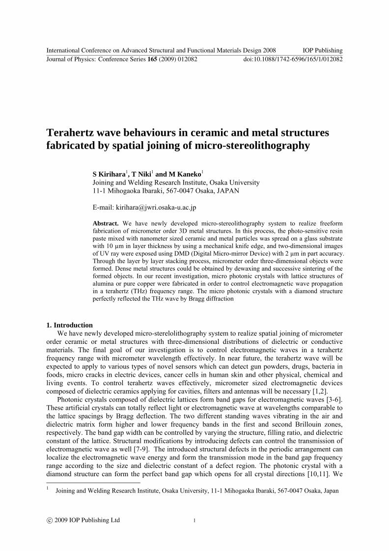
Figure 2 A dielectric photonic crystal composed of micro alumina lattices with diamond structure fabricated by using stereolithography
Figure 3 A transmission spectrum of terahertz wave for Γ-X lt100gt direction in the alumina photonic crystal with the diamond structure
Figure 4 A twinned diamond photonic crystal with a plane defect between mirror symmetric alumina lattices parallel to (100) layers
Figure 5 A localized mode of a transmission peak in a photonic band gap formed through thetwinned diamond structure of the alumina lattice
Photonic Band Gap lt Simulation gt
International Conference on Advanced Structural and Functional Materials Design 2008 IOP PublishingJournal of Physics Conference Series 165 (2009) 012082 doi1010881742-65961651012082
3
or 1000degC respectively The heating rate was 80degCmin The density of the sintered sample was measured by the Archimedes method The microstructures were observed by optical microscope and scanning electron microscopy (SEM) The transmittance and the phase shift of incident terahertz waves were measured by using terahertz time-domain spectroscopy (Advanced Infrared Spectroscopy Co Ltd Japan J-Spec2001 spcou) Measured terahertz properties were compared with simulation by using a Transmission Line Modeling (TLM) simulation program (Flomerics Micro-Stripes Ver 70) 3 Results and Discussion
Three-dimensional lattice structures composed of the alumina dispersed acrylic resin were processed exactly by using micro-stereolithography The spatial resolution was approximately 05 Figure 2 shows a (100) plane of the sintered diamond structure composed of the micrometer order alumina lattice The deformation and cracking were not observed The linear shrinkage on the horizontal axis was 238 and that on the vertical axis was 246 The relative density reached 975 Dense alumina microstructure was formed and the average grain size was approximately 2 microm The measured dielectric constant of the lattice was about 10 The terahertz wave attenuation of the transmission amplitude through the alumina diamond structure for Γ-X lt100gt crystal direction is shown in figure 3 The forbidden gap is formed at the frequency rage of from 037 to 052 THz The dotted lines show the higher and lower band gap edges calculated by using the TLM method of a finite element method The similar transmission spectra for Γ-K lt110gt and Γ-L lt111gt directions were obtained These measured results of the photonic band gap frequencies were verified to have good agreements with the simulated ones within a tolerance of 5 A common band gap was observed in every direction at the frequency range form 040 to 047 THz where the electromagnetic wave cannot transmit through the crystal and is totally reflected in all directions This common band was included in the calculated perfect photonic band gap by using a plane wave expansion (PWE) method In this theoretical calculation the plane wave propagations were simulated for all directions in the periodic arrangements of the dielectric materials by solving Maxwellrsquos equations And the photonic band distributions were drown along the symmetry lines in the Brillouin zone Figure 4 shows the twinned diamond structure composed of the mirror symmetric alumina lattices The plane defect forms parallel to the (100) crystal layer The transmission spectrum for the Γ-X lt100gt crystal direction of the twinned diamond structure is shown in figure 5 The localized mode forms in the photonic band gap At the peak frequency the incident terahertz wave localized in the plane defect and the amplified wave propagated to the opposite side The three-dimensional photonic band gap structure to form the localized mode can be applied to the terahertz wave filters
Figure 6 shows a precursor of the metal photonic crystal consisting of copper particles dispersed resin fabricated by micro-stereolithography The spatial resolution was approximately 05 By the dewaxing and sintering process full-metal diamond structures were successfully obtained Figure 7 shows the sintered samples The deformation and cracking were not observed The lattice constant of the diamond structure is 900 microm The linear shrinkage was 10 It is possible to obtain the uniform shrinkage by designing an appropriate elongated structure in the vertical direction for compensation to the gravity effect The relative density reached 897 Figure 8 shows the transmittance intensity and the phase shift spectra along Γ-X lt100gt directions Opaque regions were formed and phase shifts became discontinuous indicating the formation of photonic band gaps at the frequency range from 039 to 048 THz The band gap frequency was compared with calculations by using the TLM method as shown in figure 9 The measured opaque region corresponded to the calculation In the photonic band gap the incident wave are diffracted by multiple reflections in the periodic structure composed of the three dimensional pure copper lattices As shown in figure 8 and figure 3 the transmission spectra obtained through the pure copper metal structures and the alumina ceramic ones exhibit different profiles The electromagnetic wave can transmit with resonances and absorptions into the alumina ceramic lattices However the pure copper metal lattices reflect the wave on the surface without transmission These different behaviours of the electromagnetic wave diffractions in the periodic lattices cause the variations of band gap profiles in the transmission spectra
International Conference on Advanced Structural and Functional Materials Design 2008 IOP PublishingJournal of Physics Conference Series 165 (2009) 012082 doi1010881742-65961651012082
4
Figure 6 The diamond photonic crystal of acryl lattices with the pure copper dispersion formed by using micro-stereolithography
Figure 7 The pure copper photonic crystal with the diamond lattice structure composed of the micrometer order conductive metal rods
Figure 8 The terahertz wave transmittance and phase shift spectrum for the Γ-X lt100gt direction through the pure copper photonic crystal with the diamond lattice structure
Figure 9 The simulated transmission spectrum in the terahertz wave frequency for the photonic crystal composed of the pure copper diamond lattices by using TLM method
International Conference on Advanced Structural and Functional Materials Design 2008 IOP PublishingJournal of Physics Conference Series 165 (2009) 012082 doi1010881742-65961651012082
5
4 Conclusion We have fabricated three-dimensional micro photonic crystals with a diamond structure composed
of alumina or pure copper dispersed acrylic resin by using micro-stereolithography By the careful optimization of process parameters regarding dewaxing and sintering we have succeeded in fabricating dense alumina or pure copper micro diamond structures The sintered photonic crystals formed complete photonic band gaps at the terahertz region A twinned diamond photonic crystal composed of alumina lattices with a plane defect between mirror symmetric lattice structures was also fabricated A localized mode of transmission peak was observed in the forbidden bands In electromagnetic wave simulations the localized mode with multiple reflections was formed in the plane defect between the twinned lattice patterns These micro components of ceramic and metal photonic crystals have potentials to be used as cavities filters and antennas in a THz range
5 Acknowledgments This study was supported by Priority Assistance for the Formation of Worldwide Renowned
Centers of Research - The Global COE Program (Project Center of Excellence for Advanced Structural and Functional Materials Design) from the Ministry of Education Culture Sports Science and Technology (MEXT) Japan
6 References [1] Woodward M R Wallacel P V Arnonel D D and Linfield H E 2003 J Biological Phys 29 257 [2] Exter V M Fattinger C and Grischkowsky D 1989 Optics Lett 14 1128 [3] Yablonovitch E 1987 Phys Rev Lett 58 2059 [4] Ohtaka K 1979 Phys Rev B 19 5057-5067 [5] John S and Wang J 1990 Phys Rev Lett 64 2418 [6] Soukoulis C M 1996 Photonic Band Gap Materials (Netherlands Kluwer Academic Publsher) [7] Brown R E Parker D C Yablonovich E 1993 J Optical Society of America B 10 404 [8] Noda S Yamamoto N Kobayashi H Okano M and Tomoda K 1999 Appl Phys Lett 75 905 [9] Kawakami S 2002 Photonic Crystals (Tokyo CMC) [10] Ho H K Chan T C and Soukoulis M C 1990 Phys Rev Lett 65 3152 [11] Haus W J 1994 J Modern Optics 41 195 [12] Kirihara S Takeda W M Sakoda K Miyamoto Y 2002 Solid State Communications 124 135 [13] Miyamoto Y Kirihara S and Takeda W M 2006 Chem Lett 35 342 [14] Kirihara S Miyamoto Y 2008 Ceram Interconnect and Ceram Microsystems Technol 5 254
International Conference on Advanced Structural and Functional Materials Design 2008 IOP PublishingJournal of Physics Conference Series 165 (2009) 012082 doi1010881742-65961651012082
6
Terahertz wave behaviours in ceramic and metal structures fabricated by spatial joining of micro-stereolithography
S Kirihara1 T Niki1 and M Kaneko1 Joining and Welding Research Institute Osaka University 11-1 Mihogaoka Ibaraki 567-0047 Osaka JAPAN E-mail kiriharajwriosaka-uacjp Abstract We have newly developed micro-stereolithography system to realize freeform fabrication of micrometer order 3D metal structures In this process the photo-sensitive resin paste mixed with nanometer sized ceramic and metal particles was spread on a glass substrate with 10 microm in layer thickness by using a mechanical knife edge and two-dimensional images of UV ray were exposed using DMD (Digital Micro-mirror Device) with 2 microm in part accuracy Through the layer by layer stacking process micrometer order three-dimensional objects were formed Dense metal structures could be obtained by dewaxing and successive sintering of the formed objects In our recent investigation micro photonic crystals with lattice structures of alumina or pure copper were fabricated in order to control electromagnetic wave propagation in a terahertz (THz) frequency range The micro photonic crystals with a diamond structure perfectly reflected the THz wave by Bragg diffraction
1 Introduction We have newly developed micro-sterelolithography system to realize spatial joining of micrometer
order ceramic or metal structures with three-dimensional distributions of dielectric or conductive materials The final goal of our investigation is to control electromagnetic waves in a terahertz frequency range with micrometer wavelength effectively In near future the terahertz wave will be expected to apply to various types of novel sensors which can detect gun powders drugs bacteria in foods micro cracks in electric devices cancer cells in human skin and other physical chemical and living events To control terahertz waves effectively micrometer sized electromagnetic devices composed of dielectric ceramics applying for cavities filters and antennas will be necessary [12]
Photonic crystals composed of dielectric lattices form band gaps for electromagnetic waves [3-6] These artificial crystals can totally reflect light or electromagnetic wave at wavelengths comparable to the lattice spacings by Bragg deflection The two different standing waves vibrating in the air and dielectric matrix form higher and lower frequency bands in the first and second Brillouin zones respectively The band gap width can be controlled by varying the structure filling ratio and dielectric constant of the lattice Structural modifications by introducing defects can control the transmission of electromagnetic wave as well [7-9] The introduced structural defects in the periodic arrangement can localize the electromagnetic wave energy and form the transmission mode in the band gap frequency range according to the size and dielectric constant of a defect region The photonic crystal with a diamond structure can form the perfect band gap which opens for all crystal directions [1011] We 1 Joining and Welding Research Institute Osaka University 11-1 Mihogaoka Ibaraki 567-0047 Osaka Japan
International Conference on Advanced Structural and Functional Materials Design 2008 IOP PublishingJournal of Physics Conference Series 165 (2009) 012082 doi1010881742-65961651012082
ccopy 2009 IOP Publishing Ltd 1
have fabricated the millimeter sized dielectric photonic crystal with a diamond structure to control the microwave by using a structural joining method of stereolithography [1213] In our recent study micrometer sized alumina and pure copper lattices with a diamond structure were fabricated by using a newly developed micro-stereolithography system [14] These photonic crystals showed the perfect band gap which prohibited the terahertz wave propagation in all directions Recently we successfully fabricated a twinned diamond structure with a plane defect between mirror symmetric lattice patterns A localized mode to transmit terahertz wave selectively was formed in the photonic band gap In this study transmission spectra of terahertz wave through alumina and pure copper diamond structures were measured The selective transmission mode in the band gaps were observed for the twinned diamond structure and discussed in relation to the terahertz wave localization at the plane defect
Figure 1 A schematic illustration of micro-stereolithography 2 Experimental Procedure
The three-dimensional diamond structures were designed by using a 3D-CAD program (Toyota Caelum Co Ltd thinkdesign ver 70) In the photonic crystal with diamond structure the lattice constant was 1 mm The whole structure was 6times6times2 mm3 in size consisting of 6times6times2 unit cells The aspect ratio of the metal lattices was designed to be 15 The CAD data was converted into a STL file of a rapid prototyping format After the slicing process of 3D model into a series of two-dimensional cross-sectional data into thin sections this data was transferred to micro-stereolithographic equipment (D-MEC Co Ltd Japan SI-C10008) In our system photo sensitive acrylic resins dispersed with alumina or pure copper particles of 170nm or 5 microm in diameter at 40 or 54 vol respectively were fed over substrates from dispenser nozzles The highly viscous resin paste was fed with controlled air pressure It was spread uniformly by moving a knife edge The thickness of each layer was controlled to 10 microm A two-dimensional pattern was formed by illuminating visible laser of 405 nm in wavelength on the resin surface The high resolution has been achieved by using a Digital Micromirror Device (DMD) and an objective lens Figure 1 shows a schematic of the micro-stereolitographic system The DMD is an optical element assembled by mirrors of 14 microm in edge length The tilting of each tiny mirror can be controlled according to the two-dimensional cross sectional data by a computer The three-dimensional structures were built by stacking these patterns layer by layer In order to avoid deformation and cracking during dewaxing careful investigation for the dewaxing process was required The precursors with diamond structures were heated at various temperatures from 100degC to 600degC while the heating rate was 10 degC min The dewaxing process was observed in respect to the weight and color changes The alumina or pure copper particles could be sintered at 1500
International Conference on Advanced Structural and Functional Materials Design 2008 IOP PublishingJournal of Physics Conference Series 165 (2009) 012082 doi1010881742-65961651012082
2
Figure 2 A dielectric photonic crystal composed of micro alumina lattices with diamond structure fabricated by using stereolithography
Figure 3 A transmission spectrum of terahertz wave for Γ-X lt100gt direction in the alumina photonic crystal with the diamond structure
Figure 4 A twinned diamond photonic crystal with a plane defect between mirror symmetric alumina lattices parallel to (100) layers
Figure 5 A localized mode of a transmission peak in a photonic band gap formed through thetwinned diamond structure of the alumina lattice
Photonic Band Gap lt Simulation gt
International Conference on Advanced Structural and Functional Materials Design 2008 IOP PublishingJournal of Physics Conference Series 165 (2009) 012082 doi1010881742-65961651012082
3
or 1000degC respectively The heating rate was 80degCmin The density of the sintered sample was measured by the Archimedes method The microstructures were observed by optical microscope and scanning electron microscopy (SEM) The transmittance and the phase shift of incident terahertz waves were measured by using terahertz time-domain spectroscopy (Advanced Infrared Spectroscopy Co Ltd Japan J-Spec2001 spcou) Measured terahertz properties were compared with simulation by using a Transmission Line Modeling (TLM) simulation program (Flomerics Micro-Stripes Ver 70) 3 Results and Discussion
Three-dimensional lattice structures composed of the alumina dispersed acrylic resin were processed exactly by using micro-stereolithography The spatial resolution was approximately 05 Figure 2 shows a (100) plane of the sintered diamond structure composed of the micrometer order alumina lattice The deformation and cracking were not observed The linear shrinkage on the horizontal axis was 238 and that on the vertical axis was 246 The relative density reached 975 Dense alumina microstructure was formed and the average grain size was approximately 2 microm The measured dielectric constant of the lattice was about 10 The terahertz wave attenuation of the transmission amplitude through the alumina diamond structure for Γ-X lt100gt crystal direction is shown in figure 3 The forbidden gap is formed at the frequency rage of from 037 to 052 THz The dotted lines show the higher and lower band gap edges calculated by using the TLM method of a finite element method The similar transmission spectra for Γ-K lt110gt and Γ-L lt111gt directions were obtained These measured results of the photonic band gap frequencies were verified to have good agreements with the simulated ones within a tolerance of 5 A common band gap was observed in every direction at the frequency range form 040 to 047 THz where the electromagnetic wave cannot transmit through the crystal and is totally reflected in all directions This common band was included in the calculated perfect photonic band gap by using a plane wave expansion (PWE) method In this theoretical calculation the plane wave propagations were simulated for all directions in the periodic arrangements of the dielectric materials by solving Maxwellrsquos equations And the photonic band distributions were drown along the symmetry lines in the Brillouin zone Figure 4 shows the twinned diamond structure composed of the mirror symmetric alumina lattices The plane defect forms parallel to the (100) crystal layer The transmission spectrum for the Γ-X lt100gt crystal direction of the twinned diamond structure is shown in figure 5 The localized mode forms in the photonic band gap At the peak frequency the incident terahertz wave localized in the plane defect and the amplified wave propagated to the opposite side The three-dimensional photonic band gap structure to form the localized mode can be applied to the terahertz wave filters
Figure 6 shows a precursor of the metal photonic crystal consisting of copper particles dispersed resin fabricated by micro-stereolithography The spatial resolution was approximately 05 By the dewaxing and sintering process full-metal diamond structures were successfully obtained Figure 7 shows the sintered samples The deformation and cracking were not observed The lattice constant of the diamond structure is 900 microm The linear shrinkage was 10 It is possible to obtain the uniform shrinkage by designing an appropriate elongated structure in the vertical direction for compensation to the gravity effect The relative density reached 897 Figure 8 shows the transmittance intensity and the phase shift spectra along Γ-X lt100gt directions Opaque regions were formed and phase shifts became discontinuous indicating the formation of photonic band gaps at the frequency range from 039 to 048 THz The band gap frequency was compared with calculations by using the TLM method as shown in figure 9 The measured opaque region corresponded to the calculation In the photonic band gap the incident wave are diffracted by multiple reflections in the periodic structure composed of the three dimensional pure copper lattices As shown in figure 8 and figure 3 the transmission spectra obtained through the pure copper metal structures and the alumina ceramic ones exhibit different profiles The electromagnetic wave can transmit with resonances and absorptions into the alumina ceramic lattices However the pure copper metal lattices reflect the wave on the surface without transmission These different behaviours of the electromagnetic wave diffractions in the periodic lattices cause the variations of band gap profiles in the transmission spectra
International Conference on Advanced Structural and Functional Materials Design 2008 IOP PublishingJournal of Physics Conference Series 165 (2009) 012082 doi1010881742-65961651012082
4
Figure 6 The diamond photonic crystal of acryl lattices with the pure copper dispersion formed by using micro-stereolithography
Figure 7 The pure copper photonic crystal with the diamond lattice structure composed of the micrometer order conductive metal rods
Figure 8 The terahertz wave transmittance and phase shift spectrum for the Γ-X lt100gt direction through the pure copper photonic crystal with the diamond lattice structure
Figure 9 The simulated transmission spectrum in the terahertz wave frequency for the photonic crystal composed of the pure copper diamond lattices by using TLM method
International Conference on Advanced Structural and Functional Materials Design 2008 IOP PublishingJournal of Physics Conference Series 165 (2009) 012082 doi1010881742-65961651012082
5
4 Conclusion We have fabricated three-dimensional micro photonic crystals with a diamond structure composed
of alumina or pure copper dispersed acrylic resin by using micro-stereolithography By the careful optimization of process parameters regarding dewaxing and sintering we have succeeded in fabricating dense alumina or pure copper micro diamond structures The sintered photonic crystals formed complete photonic band gaps at the terahertz region A twinned diamond photonic crystal composed of alumina lattices with a plane defect between mirror symmetric lattice structures was also fabricated A localized mode of transmission peak was observed in the forbidden bands In electromagnetic wave simulations the localized mode with multiple reflections was formed in the plane defect between the twinned lattice patterns These micro components of ceramic and metal photonic crystals have potentials to be used as cavities filters and antennas in a THz range
5 Acknowledgments This study was supported by Priority Assistance for the Formation of Worldwide Renowned
Centers of Research - The Global COE Program (Project Center of Excellence for Advanced Structural and Functional Materials Design) from the Ministry of Education Culture Sports Science and Technology (MEXT) Japan
6 References [1] Woodward M R Wallacel P V Arnonel D D and Linfield H E 2003 J Biological Phys 29 257 [2] Exter V M Fattinger C and Grischkowsky D 1989 Optics Lett 14 1128 [3] Yablonovitch E 1987 Phys Rev Lett 58 2059 [4] Ohtaka K 1979 Phys Rev B 19 5057-5067 [5] John S and Wang J 1990 Phys Rev Lett 64 2418 [6] Soukoulis C M 1996 Photonic Band Gap Materials (Netherlands Kluwer Academic Publsher) [7] Brown R E Parker D C Yablonovich E 1993 J Optical Society of America B 10 404 [8] Noda S Yamamoto N Kobayashi H Okano M and Tomoda K 1999 Appl Phys Lett 75 905 [9] Kawakami S 2002 Photonic Crystals (Tokyo CMC) [10] Ho H K Chan T C and Soukoulis M C 1990 Phys Rev Lett 65 3152 [11] Haus W J 1994 J Modern Optics 41 195 [12] Kirihara S Takeda W M Sakoda K Miyamoto Y 2002 Solid State Communications 124 135 [13] Miyamoto Y Kirihara S and Takeda W M 2006 Chem Lett 35 342 [14] Kirihara S Miyamoto Y 2008 Ceram Interconnect and Ceram Microsystems Technol 5 254
International Conference on Advanced Structural and Functional Materials Design 2008 IOP PublishingJournal of Physics Conference Series 165 (2009) 012082 doi1010881742-65961651012082
6