Tda 10021 Datasheet
17
DATA SHEET Product specification Supersedes data of 2000 Jun 21 File under Integrated Circuits, IC02 2001 Oct 01 INTEGRATED CIRCUITS TDA10021HT DVB-C channel receiver
-
Upload
willy-daco -
Category
Documents
-
view
18 -
download
1
description
TDA10021HT
Transcript of Tda 10021 Datasheet

DATA SHEET
Product specificationSupersedes data of 2000 Jun 21File under Integrated Circuits, IC02
2001 Oct 01
INTEGRATED CIRCUITS
TDA10021HTDVB-C channel receiver

2001 Oct 01 2
Philips Semiconductors Product specification
DVB-C channel receiver TDA10021HT
FEATURES
• 4, 16, 32, 64, 128 and 256 Quadrature AmplitudeModulation (QAM) demodulator (DVB-C compatible:ETS 300-429/ITU-T J83 annex A/C)
• High performance for 256 QAM, especially for directIF applications
• On-chip 10-bit Analog-to-Digital Converter (ADC)
• On-chip Phase-Locked Loop (PLL) for crystal frequencymultiplication (typically 4 MHz crystal)
• Digital downconversion
• Programmable half Nyquist filter (roll off = 0.15 or 0.13)
• Two Pulse Width Modulated (PWM) AGC outputs withprogrammable take over point (for tuner anddownconverter control)
• Clock timing recovery, with programmable 2nd-orderloop filter
• Variable symbol rate capability from SACLK/64 toSACLK/4 (SACLK = 36 MHz maximum)
• Programmable anti-aliasing filters
• Full digital carrier recovery loop
• Carrier acquisition range up to 18% of symbol rate
• Integrated adaptive equalizer (linear transversalequalizer or decision feedback equalizer)
• On-chip Forward Error Correction (FEC) decoder(de-interleaver and RS decoder) and fully DVB-Ccompliant
• DVB compatible differential decoding and mapping
• Parallel and serial transport stream interfacesimultaneously
• I2C-bus interface, for easy control
• CMOS 0.2 µm technology.
APPLICATIONS
• Cable set-top boxes
• Cable modems
• MMDS (ETS 300-749) set-top boxes.
GENERAL DESCRIPTION
The TDA10021HT is a single-chip DVB-C channelreceiver for 4, 16, 32, 64, 128 and 256 QAM modulatedsignals. The device interfaces directly to the IF signal,which is sampled by a 10-bit ADC.
The TDA10021HT performs the clock and the carrierrecovery functions. The digital loop filters for both clockand carrier recovery are programmable in order tooptimize their characteristics according to the currentapplication.
After baseband conversion, equalization filters are usedfor echo cancellation in cable applications. These filtersare configured as either a T-spaced transversal equalizeror a Decision Feedback Equalizer (DFE), so that thesystem performance can be optimized according to thenetwork characteristics. A proprietary equalizationalgorithm, independent of carrier offset, is achieved inorder to assist carrier recovery. A decision directedalgorithm then takes place, to achieve final equalizationconvergence.
The TDA10021HT implements a FORNEY convolutionalde-interleaver of depth 12 blocks and a Reed-Solomondecoder which corrects up to 8 erroneous bytes. Thede-interleaver and the RS decoder are automaticallysynchronized by the frame synchronization algorithmwhich uses the MPEG-2 sync byte. Finally descramblingaccording to DVB-C standard, is achieved at the ReedSolomon output. This device is controlled via an I2C-bus.
Designed in 0.2 µm CMOS technology and housed in a64 pin TQFP package, the TDA10021HT operates overthe commercial temperature range.
ORDERING INFORMATION
TYPENUMBER
PACKAGE
NAME DESCRIPTION VERSION
TDA10021HT TQFP64 plastic thin quad flat package; 64 leads; body 10 × 10 × 1.0 mm SOT357-1

2001O
ct013
Philips S
emiconductors
Product specification
DV
B-C
channel receiverT
DA
10021HT
This text is here in white to force landscape pages to be rotated correctly when browsing through the pdf in the Acrobat reader.This text is here in_white to force landscape pages to be rotated correctly when browsing through the pdf in the Acrobat reader.This text is here inThis text is here inwhite to force landscape pages to be rotated correctly when browsing through the pdf in the Acrobat reader. white to force landscape pages to be ...
BLO
CK
DIA
GR
AM
handbook, full pagewidth
MGW343
CLOCKRECOVERY
I2C-BUSINTERFACE
GPIO
AGCPWM
PWM
TIMINGINTERPOLATOR
RSDECODER OUTPUT
INTERFACE
JTAG
DE-SCRAMBLERDE-INTERLEAVER
DECIMATIONFILTERS
BASEBANDCONVERSION
ADC
PLL
EQUALIZERHALF
NYQUISTCARRIER
RECOVERY
DECISIONDIFFERENTIAL
DECODER
10
8
IF
TDA10021HT
2 3 62 61 64 63 1, 24,7, 41
4, 8,25, 42
14, 30,43
15, 31,44
50 49 52 51 55, 60 56, 59 13
5
9
11
17
54
18 19
SACLK
AGCTUN
AGCIF
SCL
SDA SDAT
DEN
OCLKprogrammable
interface
serialinterface
PSYNC
UNCOR
DO[7:0]
37 to 40,45 to 48
36
35
34
33
20
21
22
23
26
27
28
32
29
21
6
16
58
57
10
SCLT
ENSERI
TCK
TDI
TRST
TMS
TDO
CTRL
GPIO
4 4 3 3 2 2
VDDD18
VSSD18
VDDD50VDDD33
VSSD33 VSSA2
VDDD1
VSSD1VCCD(PLL) PLLGND
DGND VCCA (PLL) VDDA3
VSSA3
TEST
ENSERI
IICDIV
CLR#
VIP
VIM
Vref(neg)
VDDA2
XIN XOUT
53
Vref(pos)
12
SADDR
Fig.1 Block diagram.

2001 Oct 01 4
Philips Semiconductors Product specification
DVB-C channel receiver TDA10021HT
PINNING
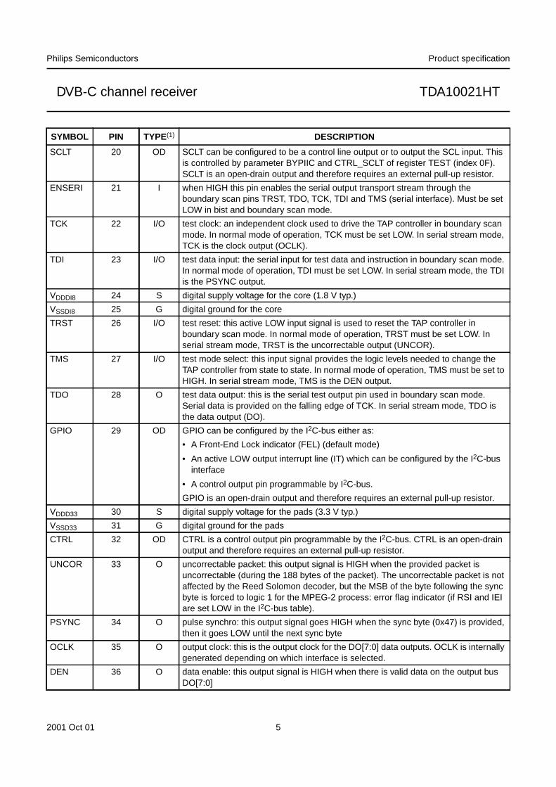
SYMBOL PIN TYPE (1) DESCRIPTION
VDDD18 1 S digital supply voltage for the core (1.8 V typ.)
XIN 2 I XTAL oscillator input pin: a fundamental XTAL oscillator is connected between theXIN and XOUT pins. The XTAL frequency must be chosen so that the systemfrequency SYSCLK (XIN × multiplying factor of the PLL) equals 1.6 times the tuneroutput intermediate frequency; i.e. SYSCLK = 1.6 × IF.
XOUT 3 O XTAL oscillator output pin: a fundamental XTAL oscillator is connected between theXIN and XOUT pins
VSSD18 4 G digital ground for the core
SACLK 5 O sampling clock: this output clock can be fed to an external 10-bit ADC as thesampling clock; SACLK = SYSCLK/2
TEST 6 I test input pin: in normal mode, pin TEST must be connected to ground
VDDD18 7 S digital supply voltage for the core (1.8 V typ.)
VSSD18 8 G digital ground for the core
AGCTUN 9 O/OD first PWM encoded output signal for AGC tuner: this signal is fed to the AGCamplifier through a single RC network. The maximum signal frequency on theVAGC output is XIN/16. AGC information is refreshed every 1024 symbols.
IICDIV 10 I IICDIV: this pin allows the frequency of the I2C-bus internal system clock to beselected, depending on the crystal frequency. The internal I2C-bus clock is adivision of XIN by 4IICDIV.
AGCIF 11 O/OD second PWM encoded output signal for the AGC IF: This signal is fed to the AGCamplifier through a single RC network. The maximum signal frequency on theVAGC output is XIN/16. AGC information is refreshed every 1024 symbols.However AGCIF can also be configured to output a PWM signal, the value of whichcan be programmed through the I2C-bus interface.
SADDR 12 I SADDR is the LSB of the I2C-bus address of the TDA10021HT. The MSBs areinternally set to 000110. Therefore the complete I2C-bus address of theTDA10021HT is (MSB to LSB) 0, 0, 0, 1, 1, 0 and SADDR.
VDDD50 13 S digital supply voltage for the pad 5.0 V (necessary for 5 V tolerant inputs)
VDDD33 14 S digital supply voltage for the pads (3.3 V typ.)
VSSD33 15 G digital ground for the pads
CLR# 16 I the CLR# input is asynchronous and active LOW, and clears the TDA10021HT:When CLR# goes LOW, the circuit immediately enters its reset mode and normaloperation will resume 4 XIN falling edges after CLR# returns HIGH. The I2C-busregister contents are all initialized to their default values. The minimum width ofCLR# at LOW level is 4 XIN clock periods.
SCL 17 I I2C-bus clock input: SCL should nominally be a square wave with a maximumfrequency of 400 kHz. SCL is generated by the system I2C-bus master.
SDA 18 I/OD SDA is a bidirectional signal: it is the serial input/output of the I2C-bus internal block.A pull-up resistor (typically 4.7 kΩ) must be connected between SDA and VDDD50 forproper operation (open-drain output).
SDAT 19 I/OD SDAT is equivalent to SDA I/O of the TDA10021HT but can be 3-stated by I2C-busprogramming. It is actually the output of a switch controlled by parameter BYPIIC ofregister TEST (index 0F). SDAT is an open-drain output and therefore requires anexternal pull-up resistor.
2001 Oct 01 5
Philips Semiconductors Product specification
DVB-C channel receiver TDA10021HT
SCLT 20 OD SCLT can be configured to be a control line output or to output the SCL input. Thisis controlled by parameter BYPIIC and CTRL_SCLT of register TEST (index 0F).SCLT is an open-drain output and therefore requires an external pull-up resistor.
ENSERI 21 I when HIGH this pin enables the serial output transport stream through theboundary scan pins TRST, TDO, TCK, TDI and TMS (serial interface). Must be setLOW in bist and boundary scan mode.
TCK 22 I/O test clock: an independent clock used to drive the TAP controller in boundary scanmode. In normal mode of operation, TCK must be set LOW. In serial stream mode,TCK is the clock output (OCLK).
TDI 23 I/O test data input: the serial input for test data and instruction in boundary scan mode.In normal mode of operation, TDI must be set LOW. In serial stream mode, the TDIis the PSYNC output.
VDDDI8 24 S digital supply voltage for the core (1.8 V typ.)
VSSDI8 25 G digital ground for the core
TRST 26 I/O test reset: this active LOW input signal is used to reset the TAP controller inboundary scan mode. In normal mode of operation, TRST must be set LOW. Inserial stream mode, TRST is the uncorrectable output (UNCOR).
TMS 27 I/O test mode select: this input signal provides the logic levels needed to change theTAP controller from state to state. In normal mode of operation, TMS must be set toHIGH. In serial stream mode, TMS is the DEN output.
TDO 28 O test data output: this is the serial test output pin used in boundary scan mode.Serial data is provided on the falling edge of TCK. In serial stream mode, TDO isthe data output (DO).
GPIO 29 OD GPIO can be configured by the I2C-bus either as:
• A Front-End Lock indicator (FEL) (default mode)
• An active LOW output interrupt line (IT) which can be configured by the I2C-businterface
• A control output pin programmable by I2C-bus.
GPIO is an open-drain output and therefore requires an external pull-up resistor.
VDDD33 30 S digital supply voltage for the pads (3.3 V typ.)
VSSD33 31 G digital ground for the pads
CTRL 32 OD CTRL is a control output pin programmable by the I2C-bus. CTRL is an open-drainoutput and therefore requires an external pull-up resistor.
UNCOR 33 O uncorrectable packet: this output signal is HIGH when the provided packet isuncorrectable (during the 188 bytes of the packet). The uncorrectable packet is notaffected by the Reed Solomon decoder, but the MSB of the byte following the syncbyte is forced to logic 1 for the MPEG-2 process: error flag indicator (if RSI and IEIare set LOW in the I2C-bus table).
PSYNC 34 O pulse synchro: this output signal goes HIGH when the sync byte (0x47) is provided,then it goes LOW until the next sync byte
OCLK 35 O output clock: this is the output clock for the DO[7:0] data outputs. OCLK is internallygenerated depending on which interface is selected.
DEN 36 O data enable: this output signal is HIGH when there is valid data on the output busDO[7:0]
SYMBOL PIN TYPE (1) DESCRIPTION

2001 Oct 01 6
Philips Semiconductors Product specification
DVB-C channel receiver TDA10021HT
Note
1. All inputs (I) are TTL, 5 V tolerant (except pins XIN, VIP and VIM). OD are open-drain outputs, so they must beconnected by a pull-up resistor to either VDDD33 or VDDD50.
DO[7:4] 37 to 40 O data output bus: this 8-bit parallel data is the output from the TDA10021HT afterdemodulation, de-interleaving, RS decoding and de-scrambling. When one of thetwo possible parallel interfaces is selected (parameter SERINT = 0, index 20) thenDO[7:0] is the transport stream output. When the serial interface is selected(parameter SERINT = 1, index 20) then the serial output is on pin DO[0].
VDDDI8 41 S digital supply voltage for the core (1.8 V typ.)
VSSD18 42 G digital ground for the core
VDDD33 43 S digital supply voltage for the pads (3.3 V typ.)
VSSD33 44 G digital ground for the pads
DO[3:0] 45 to 48 O data output bus: this 8-bit parallel data is the output from the TDA10021HT afterdemodulation, de-interleaving, RS decoding and de-scrambling. When one of thetwo possible parallel interfaces is selected then DO[7:0] is the transport streamoutput. When the serial interface is selected then the serial output is on pin DO[0].
VSSD1 49 G ground return for the digital switching circuitry (ADC)
VDDD1 50 S power supply input for the digital switching circuitry 1.8 V (ADC)
VSSA2 51 G ground return for the analog clock drivers (ADC)
VDDA2 52 S power supply input for the analog clock drivers 3.3 V (ADC)
Vref(pos) 53 O this is a positive voltage reference for the ADC. It is derived from the internal bandgap voltage, VBG, with an on-chip fully differential amplifier.
Vref(neg) 54 O this is the negative voltage reference for the ADC. It is derived from the internalband gap voltage, VBG, with an on-chip fully differential amplifier.
VDDA3 55 S power supply input for the analog circuits 3.3 V (ADC)
VSSA3 56 G ground return for analog circuits (ADC)
VIM 57 I negative input to the ADC: this pin is DC biased to half-supply through an internalresistor divider (2 × 20 kΩ resistors). In order to stay in the range of the ADC,VIP − VIM should remain between the input range corresponding to the SWregister (index 1B − default value = 0.5 V).
VIP 58 I positive input to the ADC: this pin is DC biased to half-supply through an internalresistor divider (2 × 20 kΩ resistors). In order to stay in the range of the ADC,VIP − VIM should remain between the input range corresponding to the SWregister (index 1B − default value = 0.5 V).
VSSA3 59 G ground return for analog circuits (ADC)
VDDA3 60 S power supply input for the analog circuits 3.3 V (ADC)
VCCD(PLL) 61 S power supply for the PLL digital section 1.8 V
DGND 62 G ground connection for the PLL digital section
PLLGND 63 G ground connection for the PLL analog section
VCCA(PLL) 64 S power supply for the PLL analog section 3.3 V
SYMBOL PIN TYPE (1) DESCRIPTION
2001 Oct 01 7
Philips Semiconductors Product specification
DVB-C channel receiver TDA10021HT
handbook, full pagewidth
TDA10021HT
MGW344
1
2
3
4
5
6
7
8
9
10
11
12
13
14
15
16
48
47
46
45
44
43
42
41
40
39
38
37
36
35
34
33
17
18
19 20
21
22
23
24
25
26
27
28
29
30
31
32
64
63
62
61
60
59
58
57
56
55
54
53
52
51
50
49
VDDD18
XIN
XOUT
VSSD18
SACLK
TEST
VDDD18
VSSD18
AGCTUN
IICDIV
AGCIF
SADDR
VDDD50
VDDD33
VSSD33
CLR#
SC
L
SD
A
SD
AT
VS
SA
2
VD
DD
1
VS
SD
1
DO[0]
DO[1]
DO[2]
DO[3]
VSSD33
VDDD33
VSSD18
VDDD18
DO[4]
DO[5]
DO[6]
DO[7]
DEN
OCLK
PSYNC
UNCOR
VC
CA
(PL
L)
PL
LG
ND
DG
ND
VC
CD
(PL
L)
VD
DA
3
VS
SA
3
VIP
VIM
VS
SA
3
VD
DA
3
Vre
f(n
eg
)
Vre
f(p
os)
VD
DA
2
SC
LT
EN
SE
RI
TC
K
TD
I
VD
DD
18
VS
SD
18
TR
ST
TM
S
TD
O
GP
IO
VD
DD
33
VS
SD
33
CT
RL
Fig.1 Pin configuration.
2001 Oct 01 8
Philips Semiconductors Product specification
DVB-C channel receiver TDA10021HT
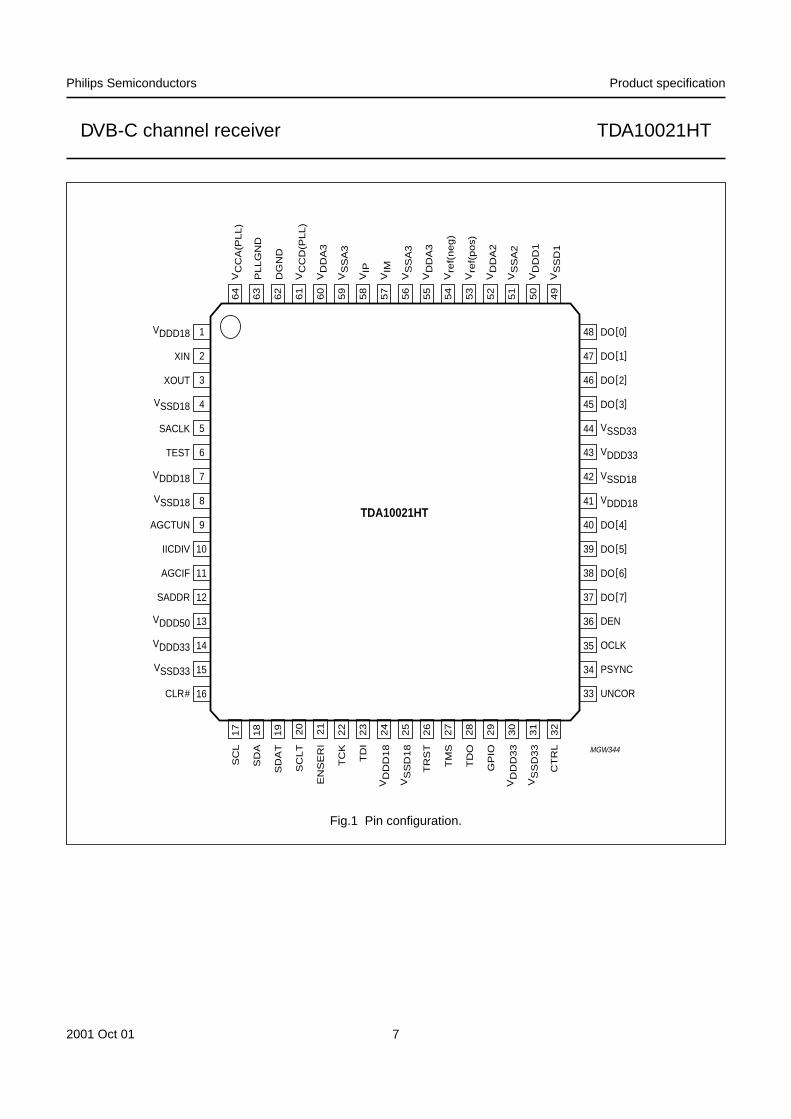
CHARACTERISTICS
Notes
1. The voltage level of the 5 V supply must always exceed or at least equal the voltage level of the 3.3 V supply duringpower-up and power-down in order to guarantee protection against latch-up.
2. All digital inputs are 5 V tolerant except pin XIN.
3. IOH, IOL = ±4 mA for pins SACLK, SCL, SDA, SDAT, SCLT, TCK, TDI, TRST, TMS, TDO, GPIO, UNCOR, PSYNC,OCLK, DEN and DO[7:0]. For all other pins, IOH, IOL = ±2 mA.
SYMBOL PARAMETER CONDITIONS MIN. TYP. MAX. UNIT
VDDD33 digital supply voltage for thepads
VDDD = 3.3 V ±10% 2.97 3.3 3.63 V
VDDD18 digital supply voltage for thecore
VDDD = 1.8 V ±5% 1.7 1.8 1.9 V
VDDD50 digital supply voltage only for 5 Vrequirements; note 1
4.75 5.0 5.25 V
VIH HIGH-level input voltage TTL input; note 2 2 − VDDD50 V
VIL LOW-level input voltage TTL input 0 − 0.8 V
VOH HIGH-level output voltage note 3 2.4 − − V
VOL LOW-level output voltage − − 0.4 V
IDDD33 digital supply current for thepads
fs = 28.92 MHz;symbol rate = 7 Mbaud
− 46 − mA
IDDD18 digital supply current for thecore
fs = 28.92 MHz;symbol rate = 7 Mbaud
− 120 − mA
Ptot total power dissipation fs = 28.92 MHz;symbol rate = 7 Mbaud
− 540 − mW
Ci input capacitance − − 5 pF
Tamb ambient temperature 0 − 70 °C
XTAL; pin XIN
VIH HIGH-level input voltage 0.7VDDD33 − VDDD33 V
VIL LOW-level input voltage 0 − 0.3VDDD33 V
PLL
VDDD(PLL) digital PLL supply voltage VDDD = 1.8 V ±5% 1.7 1.8 1.9 V
VDDA(PLL) analog PLL supply voltage VDDA = 3.3 V ±10% 2.97 3.3 3.63 V
ADC
VDDA1 analog ADC supply voltage VDDA = 1.8 V ±5% 1.7 1.8 1.9 V
VDDA2,VDDA3 analog ADC supply voltage VDDA = 3.3 V ±10% 2.97 3.3 3.63 V
VIP,VIM analog ADC inputs −0.5 − VDDA3 + 0.5 V
Vi signal input range IR = VIP − VIM −0.5 to −1.0 − +0.5 to +1.0 V
Vref(pos) positive reference voltage 1.95 2.15 2.35 V
Vref(neg) negative reference voltage 0.95 1.15 1.35 V
Voffset input offset voltage −25 − +25 mV
Ri input resistance (VIP or VIM) − 10 − kΩCi input capacitance (VIP or VIM) − 5 10 pF
B input full power bandwidth 3 dB bandwidth 40 50 − MHz

2001 Oct 01 9
Philips Semiconductors Product specification
DVB-C channel receiver TDA10021HT
APPLICATION INFORMATION
handbook, full pagewidth
MGW346I2C-BUS
I2C-bus tuner
OUTPUT1(1)
OUTPUT2(2)
ANALOGCIRCUITRY
AGC2CIRCUITRY
TUNERIF
RFinput
TDA10021HT
DEN
OCLK
PSYNC
UNCORVIP
VIM
SCLT, SDATSCL, SDA
AGCIF AGCTUN XIN XOUT
TCK (OCLK)
TDI (PSYNC)
TRST (UNCOR)
TMS (DEN)
TDO (DO)
DO[7:0]
AGC1CIRCUITRY
Fig.2 Front-end receiver schematic.
(1) Output 1 can be either a parallel output mode A, a parallel output mode B or a serial output (programmable interface).
(2) Output 2 is a serial output (serial interface).

2001 Oct 01 10
Philips Semiconductors Product specification
DVB-C channel receiver TDA10021HT
handbook, halfpage
MGW347
R2 3
XTAL
C2
XOUTXIN
C1
TDA10021HT
Fig.3 Typical XTAL connection.
(1) Typical XTAL is at fundamental frequency (typically 4 Mhz).
(2) Values of passive components are dependant on XTAL manufacturer (typically R = 1 MΩ, C1 = C2 = 56 pF).
handbook, halfpage
MGW348
R911
C
to TUNER/IF
GND
AGCTUN/AGCIF
TDA10021HT
Fig.4 External AGC connection.
R and C are chosen to verify < fc < with R = 1.5 kΩ and C = 1 nF, fc = 100 kHz.SR1024-------------
XIN16----------

2001 Oct 01 11
Philips Semiconductors Product specification
DVB-C channel receiver TDA10021HT
handbook, full pagewidth 1 Ω
0.1 µF
0.1 µF
10nF
64
63
62
61
60
59
58
57
53
54
52
51
50
49
10µF
100nF
100nF
TDA10021HT
+3.3 V
1 Ω
10nF
10µF
+1.8 V
1 Ω
10nF
10µF
+3.3 V
1 Ω
10nF
10µF
+3.3 V
1 Ω
10nF
10µF
+1.8 V
VSSA2
VDDD1
VSSD1
VCCA(PLL)
PLLGND
DGND
VCCD(PLL)
VDDA3
VSSA3
VIP
VIM
VINP
VINM
Vref(neg)
Vref(pos)
VDDA2
MGW349
Fig.5 PLL and ADC connections.
2001 Oct 01 12
Philips Semiconductors Product specification
DVB-C channel receiver TDA10021HT
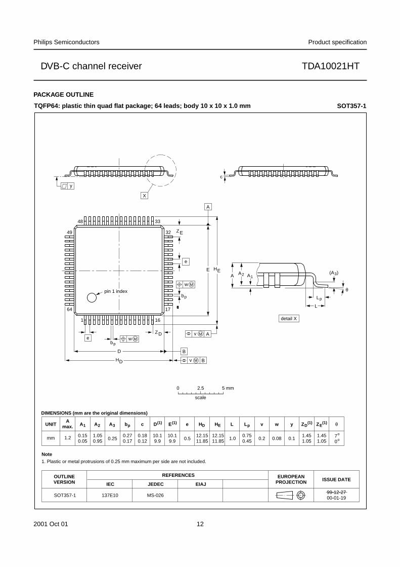
PACKAGE OUTLINE
UNITA
max. A1 A2 A3 bp c E(1) e HE L Lp Zywv θ
REFERENCESOUTLINEVERSION
EUROPEANPROJECTION ISSUE DATE
IEC JEDEC EIAJ
mm 1.2 0.150.05
1.050.95 0.25
0.270.17
0.180.12
10.19.9 0.5
12.1511.85
1.451.05
70
o
o0.08 0.11.0 0.2
DIMENSIONS (mm are the original dimensions)
Note
1. Plastic or metal protrusions of 0.25 mm maximum per side are not included.
0.750.45
SOT357-1 137E10 MS-02699-12-2700-01-19
D(1) (1)(1)
10.19.9
HD
12.1511.85
EZ
1.451.05
D
bpe
θ
EA1A
Lp
detail X
L
(A )3
B
16
c
DH
bp
EHA2
v M B
D
ZD
A
ZE
e
v M A
X
1
64
49
48 33
32
17
y
pin 1 index
w M
w M
0 2.5 5 mm
scale
TQFP64: plastic thin quad flat package; 64 leads; body 10 x 10 x 1.0 mm SOT357-1

2001 Oct 01 13
Philips Semiconductors Product specification
DVB-C channel receiver TDA10021HT
SOLDERING
Introduction to soldering surface mount packages
This text gives a very brief insight to a complex technology.A more in-depth account of soldering ICs can be found inour “Data Handbook IC26; Integrated Circuit Packages”(document order number 9398 652 90011).
There is no soldering method that is ideal for all surfacemount IC packages. Wave soldering can still be used forcertain surface mount ICs, but it is not suitable for fine pitchSMDs. In these situations reflow soldering isrecommended.
Reflow soldering
Reflow soldering requires solder paste (a suspension offine solder particles, flux and binding agent) to be appliedto the printed-circuit board by screen printing, stencilling orpressure-syringe dispensing before package placement.
Several methods exist for reflowing; for example,convection or convection/infrared heating in a conveyortype oven. Throughput times (preheating, soldering andcooling) vary between 100 and 200 seconds dependingon heating method.
Typical reflow peak temperatures range from215 to 250 °C. The top-surface temperature of thepackages should preferable be kept below 220 °C forthick/large packages, and below 235 °C for small/thinpackages.
Wave soldering
Conventional single wave soldering is not recommendedfor surface mount devices (SMDs) or printed-circuit boardswith a high component density, as solder bridging andnon-wetting can present major problems.
To overcome these problems the double-wave solderingmethod was specifically developed.
If wave soldering is used the following conditions must beobserved for optimal results:
• Use a double-wave soldering method comprising aturbulent wave with high upward pressure followed by asmooth laminar wave.
• For packages with leads on two sides and a pitch (e):
– larger than or equal to 1.27 mm, the footprintlongitudinal axis is preferred to be parallel to thetransport direction of the printed-circuit board;
– smaller than 1.27 mm, the footprint longitudinal axismust be parallel to the transport direction of theprinted-circuit board.
The footprint must incorporate solder thieves at thedownstream end.
• For packages with leads on four sides, the footprint mustbe placed at a 45° angle to the transport direction of theprinted-circuit board. The footprint must incorporatesolder thieves downstream and at the side corners.
During placement and before soldering, the package mustbe fixed with a droplet of adhesive. The adhesive can beapplied by screen printing, pin transfer or syringedispensing. The package can be soldered after theadhesive is cured.
Typical dwell time is 4 seconds at 250 °C.A mildly-activated flux will eliminate the need for removalof corrosive residues in most applications.
Manual soldering
Fix the component by first soldering twodiagonally-opposite end leads. Use a low voltage (24 V orless) soldering iron applied to the flat part of the lead.Contact time must be limited to 10 seconds at up to300 °C.
When using a dedicated tool, all other leads can besoldered in one operation within 2 to 5 seconds between270 and 320 °C.

2001 Oct 01 14
Philips Semiconductors Product specification
DVB-C channel receiver TDA10021HT
Suitability of surface mount IC packages for wave and reflow soldering methods
Notes
1. All surface mount (SMD) packages are moisture sensitive. Depending upon the moisture content, the maximumtemperature (with respect to time) and body size of the package, there is a risk that internal or external packagecracks may occur due to vaporization of the moisture in them (the so called popcorn effect). For details, refer to theDrypack information in the “Data Handbook IC26; Integrated Circuit Packages; Section: Packing Methods”.
2. These packages are not suitable for wave soldering as a solder joint between the printed-circuit board and heatsink(at bottom version) can not be achieved, and as solder may stick to the heatsink (on top version).
3. If wave soldering is considered, then the package must be placed at a 45° angle to the solder wave direction.The package footprint must incorporate solder thieves downstream and at the side corners.
4. Wave soldering is only suitable for LQFP, TQFP and QFP packages with a pitch (e) equal to or larger than 0.8 mm;it is definitely not suitable for packages with a pitch (e) equal to or smaller than 0.65 mm.
5. Wave soldering is only suitable for SSOP and TSSOP packages with a pitch (e) equal to or larger than 0.65 mm; it isdefinitely not suitable for packages with a pitch (e) equal to or smaller than 0.5 mm.
DATA SHEET STATUS
Notes
1. Please consult the most recently issued data sheet before initiating or completing a design.
2. The product status of the device(s) described in this data sheet may have changed since this data sheet waspublished. The latest information is available on the Internet at URL http://www.semiconductors.philips.com.
PACKAGESOLDERING METHOD
WAVE REFLOW (1)
BGA, HBGA, LFBGA, SQFP, TFBGA not suitable suitable
HBCC, HLQFP, HSQFP, HSOP, HTQFP, HTSSOP, HVQFN, SMS not suitable(2) suitable
PLCC(3), SO, SOJ suitable suitable
LQFP, QFP, TQFP not recommended(3)(4) suitable
SSOP, TSSOP, VSO not recommended(5) suitable
DATA SHEET STATUS (1) PRODUCTSTATUS(2) DEFINITIONS
Objective specification Development This data sheet contains data from the objective specification for productdevelopment. Philips Semiconductors reserves the right to change thespecification in any manner without notice.
Preliminary specification Qualification This data sheet contains data from the preliminary specification.Supplementary data will be published at a later date. PhilipsSemiconductors reserves the right to change the specification withoutnotice, in order to improve the design and supply the best possibleproduct.
Product specification Production This data sheet contains data from the product specification. PhilipsSemiconductors reserves the right to make changes at any time in orderto improve the design, manufacturing and supply. Changes will becommunicated according to the Customer Product/Process ChangeNotification (CPCN) procedure SNW-SQ-650A.

2001 Oct 01 15
Philips Semiconductors Product specification
DVB-C channel receiver TDA10021HT
DEFINITIONS
Short-form specification The data in a short-formspecification is extracted from a full data sheet with thesame type number and title. For detailed information seethe relevant data sheet or data handbook.
Limiting values definition Limiting values given are inaccordance with the Absolute Maximum Rating System(IEC 60134). Stress above one or more of the limitingvalues may cause permanent damage to the device.These are stress ratings only and operation of the deviceat these or at any other conditions above those given in theCharacteristics sections of the specification is not implied.Exposure to limiting values for extended periods mayaffect device reliability.
Application information Applications that aredescribed herein for any of these products are forillustrative purposes only. Philips Semiconductors makeno representation or warranty that such applications will besuitable for the specified use without further testing ormodification.
DISCLAIMERS
Life support applications These products are notdesigned for use in life support appliances, devices, orsystems where malfunction of these products canreasonably be expected to result in personal injury. PhilipsSemiconductors customers using or selling these productsfor use in such applications do so at their own risk andagree to fully indemnify Philips Semiconductors for anydamages resulting from such application.
Right to make changes Philips Semiconductorsreserves the right to make changes, without notice, in theproducts, including circuits, standard cells, and/orsoftware, described or contained herein in order toimprove design and/or performance. PhilipsSemiconductors assumes no responsibility or liability forthe use of any of these products, conveys no licence or titleunder any patent, copyright, or mask work right to theseproducts, and makes no representations or warranties thatthese products are free from patent, copyright, or maskwork right infringement, unless otherwise specified.
ICs with MPEG-2 functionality Use of this product inany manner that complies with the MPEG-2 Standard isexpressly prohibited without a license under applicablepatents in the MPEG-2 patent portfolio, which license isavailable from MPEG LA, L.L.C., 250 Steele Street, Suite300, Denver, Colorado 80206.
PURCHASE OF PHILIPS I2C COMPONENTS
Purchase of Philips I2C components conveys a license under the Philips’ I2C patent to use thecomponents in the I2C system provided the system conforms to the I2C specification defined byPhilips. This specification can be ordered using the code 9398 393 40011.

© Koninklijke Philips Electronics N.V. 2001 SCA73
All rights are reserved. Reproduction in whole or in part is prohibited without the prior written consent of the copyright owner.
The information presented in this document does not form part of any quotation or contract, is believed to be accurate and reliable and may be changedwithout notice. No liability will be accepted by the publisher for any consequence of its use. Publication thereof does not convey nor imply any licenseunder patent- or other industrial or intellectual property rights.
Philips Semiconductors – a worldwide company
Contact information
For additional information please visit http://www.semiconductors.philips.com . Fax: +31 40 27 24825For sales offices addresses send e-mail to: [email protected] .
Printed in The Netherlands 753504/04/pp16 Date of release: 2001 Oct 01 Document order number: 9397 750 08497

This datasheet has been download from:
www.datasheetcatalog.com
Datasheets for electronics components.