Tactical Grade, Six Degrees of Freedom Inertial Sensor ... · PDF fileTactical Grade, Six...
39
Tactical Grade, Six Degrees of Freedom Inertial Sensor Data Sheet ADIS16497 Rev. A Document Feedback Information furnished by Analog Devices is believed to be accurate and reliable. However, no responsibility is assumed by Analog Devices for its use, nor for any infringements of patents or other rights of third parties that may result from its use. Specifications subject to change without notice. No license is granted by implication or otherwise under any patent or patent rights of Analog Devices. Trademarks and registered trademarks are the property of their respective owners. One Technology Way, P.O. Box 9106, Norwood, MA 02062-9106, U.S.A. Tel: 781.329.4700 ©2017 Analog Devices, Inc. All rights reserved. Technical Support www.analog.com FEATURES Triaxial, digital gyroscope ±125°/sec, ±450°/sec, ±2000°/sec range options ±0.05° axis to axis misalignment error ±0.25° (maximum) axis to package misalignment error 0.8°/hr in-run bias stability 0.09°/√hr angular random walk Triaxial, digital accelerometer, ±40 g 13 μg in run bias stability Triaxial, delta angle and delta velocity outputs Factory calibrated sensitivity, bias, and axial alignment Calibration temperature range: −40°C to +85°C SPI compatible Programmable operation and control Automatic and manual bias correction controls Configurable FIR filters Digital I/O: data ready, external clock Sample clock options: internal, external, or scaled On demand self test of inertial sensors Single-supply operation: 3.0 V to 3.6 V 1500 g mechanical shock survivability Operating temperature range: −40°C to +105°C APPLICATIONS Precision instrumentation, stabilization Guidance, navigation, control Avionics, unmanned vehicles Precision autonomous machines, robotics GENERAL DESCRIPTION The ADIS16497 is a complete inertial system that includes a triaxis gyroscope and a triaxis accelerometer. Each inertial sensor in the ADIS16497 combines industry leading iMEMS® technology with signal conditioning that optimizes dynamic performance. The factory calibration characterizes each sensor for sensitivity, bias, alignment, and linear acceleration (gyroscope bias). As a result, each sensor has its own dynamic compensation formulas that provide accurate sensor measurements. The ADIS16497 provides a simple, cost effective method for integrating accurate, multiaxis inertial sensing into industrial systems, especially when compared with the complexity and investment associated with discrete designs. All necessary motion testing and calibration are part of the production process at the factory, greatly reducing system integration time. Tight orthogonal alignment simplifies inertial frame alignment in navigation systems. The serial peripheral interface (SPI) and register structure provide a simple interface for data collection and configuration control. The footprint and connector system of the ADIS16497 enable a simple upgrade from the ADIS16375, ADIS16480, ADIS16485, ADIS16488A, and ADIS16490. The ADIS16497 is available in an aluminum package that is approximately 47 mm × 44 mm × 14 mm and includes a standard connector interface. FUNCTIONAL BLOCK DIAGRAM CONTROLLER CLOCK POWER MANAGEMENT CS SCLK DIN DOUT GND VDD DIO1 DIO2 DIO3 DIO4 RST SPI SELF TEST I/O OUTPUT DATA REGISTERS USER CONTROL REGISTERS CALIBRATION AND FILTERS ADIS16497 15061-001 TRIAXIAL GYROSCOPE TEMPERATURE SENSOR TRIAXIAL ACCELEROMETER Figure 1.
Transcript of Tactical Grade, Six Degrees of Freedom Inertial Sensor ... · PDF fileTactical Grade, Six...
Tactical Grade, Six Degrees of Freedom Inertial Sensor
Data Sheet ADIS16497
Rev. A Document Feedback Information furnished by Analog Devices is believed to be accurate and reliable. However, no responsibility is assumed by Analog Devices for its use, nor for any infringements of patents or other rights of third parties that may result from its use. Specifications subject to change without notice. No license is granted by implication or otherwise under any patent or patent rights of Analog Devices. Trademarks and registered trademarks are the property of their respective owners.
One Technology Way, P.O. Box 9106, Norwood, MA 02062-9106, U.S.A. Tel: 781.329.4700 ©2017 Analog Devices, Inc. All rights reserved. Technical Support www.analog.com
FEATURES Triaxial, digital gyroscope
±125°/sec, ±450°/sec, ±2000°/sec range options ±0.05° axis to axis misalignment error ±0.25° (maximum) axis to package misalignment error 0.8°/hr in-run bias stability 0.09°/√hr angular random walk
Triaxial, digital accelerometer, ±40 g 13 μg in run bias stability
Triaxial, delta angle and delta velocity outputs Factory calibrated sensitivity, bias, and axial alignment
Calibration temperature range: −40°C to +85°C SPI compatible Programmable operation and control
Automatic and manual bias correction controls Configurable FIR filters Digital I/O: data ready, external clock Sample clock options: internal, external, or scaled On demand self test of inertial sensors
Single-supply operation: 3.0 V to 3.6 V 1500 g mechanical shock survivability Operating temperature range: −40°C to +105°C
APPLICATIONS Precision instrumentation, stabilization Guidance, navigation, control Avionics, unmanned vehicles Precision autonomous machines, robotics
GENERAL DESCRIPTION The ADIS16497 is a complete inertial system that includes a triaxis gyroscope and a triaxis accelerometer. Each inertial sensor in the ADIS16497 combines industry leading iMEMS® technology with signal conditioning that optimizes dynamic performance. The factory calibration characterizes each sensor for sensitivity, bias, alignment, and linear acceleration (gyroscope bias). As a result, each sensor has its own dynamic compensation formulas that provide accurate sensor measurements.
The ADIS16497 provides a simple, cost effective method for integrating accurate, multiaxis inertial sensing into industrial systems, especially when compared with the complexity and investment associated with discrete designs. All necessary motion testing and calibration are part of the production process at the factory, greatly reducing system integration time. Tight orthogonal alignment simplifies inertial frame alignment in navigation systems. The serial peripheral interface (SPI) and register structure provide a simple interface for data collection and configuration control.
The footprint and connector system of the ADIS16497 enable a simple upgrade from the ADIS16375, ADIS16480, ADIS16485, ADIS16488A, and ADIS16490. The ADIS16497 is available in an aluminum package that is approximately 47 mm × 44 mm × 14 mm and includes a standard connector interface.
FUNCTIONAL BLOCK DIAGRAM
CONTROLLER
CLOCK
POWERMANAGEMENT
CS
SCLK
DIN
DOUT
GND
VDDDIO1 DIO2 DIO3 DIO4 RST
SPI
SELF TEST I/O
OUTPUTDATA
REGISTERS
USERCONTROL
REGISTERS
CALIBRATIONAND
FILTERS
ADIS16497
1506
1-00
1
TRIAXIALGYROSCOPE
TEMPERATURESENSOR
TRIAXIALACCELEROMETER
Figure 1.
ADIS16497 Data Sheet
Rev. A | Page 2 of 39
TABLE OF CONTENTS Features .............................................................................................. 1 Applications ....................................................................................... 1 General Description ......................................................................... 1 Functional Block Diagram .............................................................. 1 Revision History ............................................................................... 2 Specifications ..................................................................................... 3
Timing Specifications .................................................................. 5 Absolute Maximum Ratings ............................................................ 7
Thermal Resistance ...................................................................... 7 ESD Caution .................................................................................. 7
Pin Configuration and Function Descriptions ............................. 8 Typical Performance Characteristics ............................................. 9 Theory of Operation ...................................................................... 10
Inertial Sensor Signal Chain ..................................................... 10 Register Structure ....................................................................... 11 Serial Peripheral Interface ......................................................... 12 Data Ready .................................................................................. 12 Reading Sensor Data .................................................................. 13 Device Configuration ................................................................ 14
User Register Memory Map .......................................................... 15 User Register Defintions ................................................................ 18
Page Number (PAGE_ID) ......................................................... 18 Data/Sample Counter (DATA_CNT) ...................................... 18 Status/Error Flag Indicators (SYS_E_FLAG) .......................... 18 Self Test Error Flags (DIAG_STS) ............................................ 19 Internal Temperature (TEMP_OUT) ...................................... 19 Gyroscope Data .......................................................................... 19 Acceleration Data ....................................................................... 21
Time Stamp ................................................................................. 22 Cyclical Redundandcy check (CRC-32) .................................. 22 Delta Angles ................................................................................ 23 Delta Velocity .............................................................................. 24 User Bias/Scale Adjustment ...................................................... 26 Scratch Registers, USER_SCR_x .............................................. 29 Flash Memory Endurance Counter, FLSHCNT_LOW, FLSHCNT_HIGH ...................................................................... 29 Global Commands, GLOB_CMD ............................................ 30 Auxiliary I/O Line Configuration, FNCTIO_CTRL ............. 31 General-Purpose I/O Control, GPIO_CTRL ......................... 32 Miscellaneous Configuration, CONFIG ................................. 32 Linear Acceleration on Effect on Gyroscope Bias ................. 32 Decimation Filter, DEC_RATE ................................................ 32 Continuous Bias Estimation (CBE), NULL_CNFG .............. 33 Scaling the Input Clock (PPS Mode), SYNC_SCALE ........... 33 FIR Filters .................................................................................... 34 Firmware Revision, FIRM_REV .............................................. 36 Firmware Revision Year, FIRM_Y ........................................... 36 Boot Revision Number, BOOT_REV ...................................... 36 Continuous SRAM Testing ....................................................... 36
Applications Information .............................................................. 38 Mounting Best Practices ............................................................ 38 Preventing Misinsertion ............................................................ 38 Evaluation Tools ......................................................................... 38 Power Supply Considerations ................................................... 38
Outline Dimensions ....................................................................... 39 Ordering Guide .......................................................................... 39
REVISION HISTORY 11/2017—Rev. 0 to Rev. A Changes to Table 1 ............................................................................ 3 Changed t2 Parameter, Table 2; GLOB_CMD, Bit 3 Parameter, GLOB_CMD, Bit 6 Parameter, and GLOB_CMD, Bit 7 Parameter, Table 3 ................................................................................................ 5
10/2017—Revision 0: Initial Version
Data Sheet ADIS16497
Rev. A | Page 3 of 39
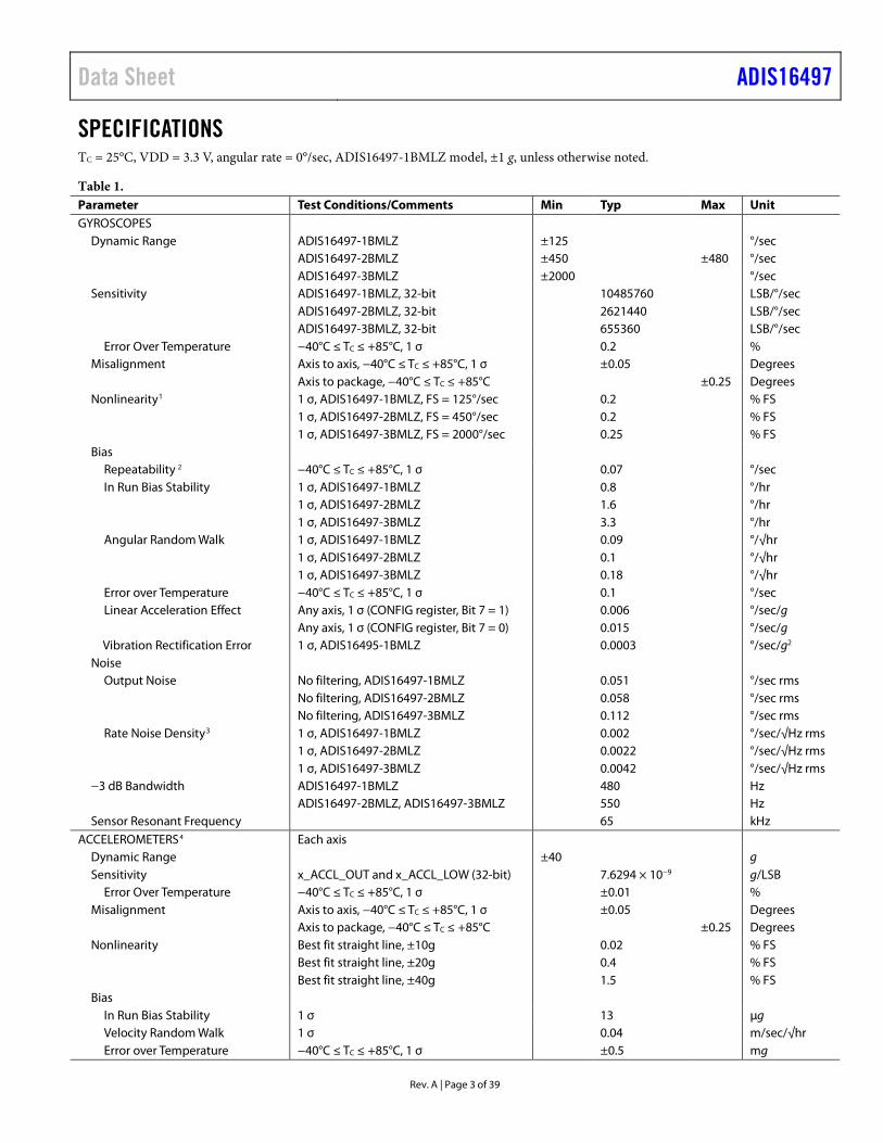
SPECIFICATIONS TC = 25°C, VDD = 3.3 V, angular rate = 0°/sec, ADIS16497-1BMLZ model, ±1 g, unless otherwise noted.
Table 1. Parameter Test Conditions/Comments Min Typ Max Unit GYROSCOPES
Dynamic Range ADIS16497-1BMLZ ±125 °/sec ADIS16497-2BMLZ ±450 ±480 °/sec ADIS16497-3BMLZ ±2000 °/sec
Sensitivity ADIS16497-1BMLZ, 32-bit 10485760 LSB/°/sec ADIS16497-2BMLZ, 32-bit 2621440 LSB/°/sec ADIS16497-3BMLZ, 32-bit 655360 LSB/°/sec
Error Over Temperature −40°C ≤ TC ≤ +85°C, 1 σ 0.2 % Misalignment Axis to axis, −40°C ≤ TC ≤ +85°C, 1 σ ±0.05 Degrees
Axis to package, −40°C ≤ TC ≤ +85°C ±0.25 Degrees Nonlinearity1 1 σ, ADIS16497-1BMLZ, FS = 125°/sec 0.2 % FS
1 σ, ADIS16497-2BMLZ, FS = 450°/sec 0.2 % FS 1 σ, ADIS16497-3BMLZ, FS = 2000°/sec 0.25 % FS
Bias Repeatability 2 −40°C ≤ TC ≤ +85°C, 1 σ 0.07 °/sec In Run Bias Stability 1 σ, ADIS16497-1BMLZ 0.8 °/hr
1 σ, ADIS16497-2BMLZ 1.6 °/hr 1 σ, ADIS16497-3BMLZ 3.3 °/hr
Angular Random Walk 1 σ, ADIS16497-1BMLZ 0.09 °/√hr 1 σ, ADIS16497-2BMLZ 0.1 °/√hr 1 σ, ADIS16497-3BMLZ 0.18 °/√hr
Error over Temperature −40°C ≤ TC ≤ +85°C, 1 σ 0.1 °/sec Linear Acceleration Effect Any axis, 1 σ (CONFIG register, Bit 7 = 1) 0.006 °/sec/g
Any axis, 1 σ (CONFIG register, Bit 7 = 0) 0.015 °/sec/g Vibration Rectification Error 1 σ, ADIS16495-1BMLZ 0.0003 °/sec/g2
Noise Output Noise No filtering, ADIS16497-1BMLZ 0.051 °/sec rms
No filtering, ADIS16497-2BMLZ 0.058 °/sec rms No filtering, ADIS16497-3BMLZ 0.112 °/sec rms
Rate Noise Density3 1 σ, ADIS16497-1BMLZ 0.002 °/sec/√Hz rms 1 σ, ADIS16497-2BMLZ 0.0022 °/sec/√Hz rms 1 σ, ADIS16497-3BMLZ 0.0042 °/sec/√Hz rms
−3 dB Bandwidth ADIS16497-1BMLZ 480 Hz ADIS16497-2BMLZ, ADIS16497-3BMLZ 550 Hz
Sensor Resonant Frequency 65 kHz ACCELEROMETERS4 Each axis
Dynamic Range ±40 g Sensitivity x_ACCL_OUT and x_ACCL_LOW (32-bit) 7.6294 × 10⁻⁹ g/LSB
Error Over Temperature −40°C ≤ TC ≤ +85°C, 1 σ ±0.01 % Misalignment Axis to axis, −40°C ≤ TC ≤ +85°C, 1 σ ±0.05 Degrees
Axis to package, −40°C ≤ TC ≤ +85°C ±0.25 Degrees Nonlinearity Best fit straight line, ±10g 0.02 % FS
Best fit straight line, ±20g 0.4 % FS Best fit straight line, ±40g 1.5 % FS
Bias In Run Bias Stability 1 σ 13 μg Velocity Random Walk 1 σ 0.04 m/sec/√hr Error over Temperature −40°C ≤ TC ≤ +85°C, 1 σ ±0.5 mg
ADIS16497 Data Sheet
Rev. A | Page 4 of 39
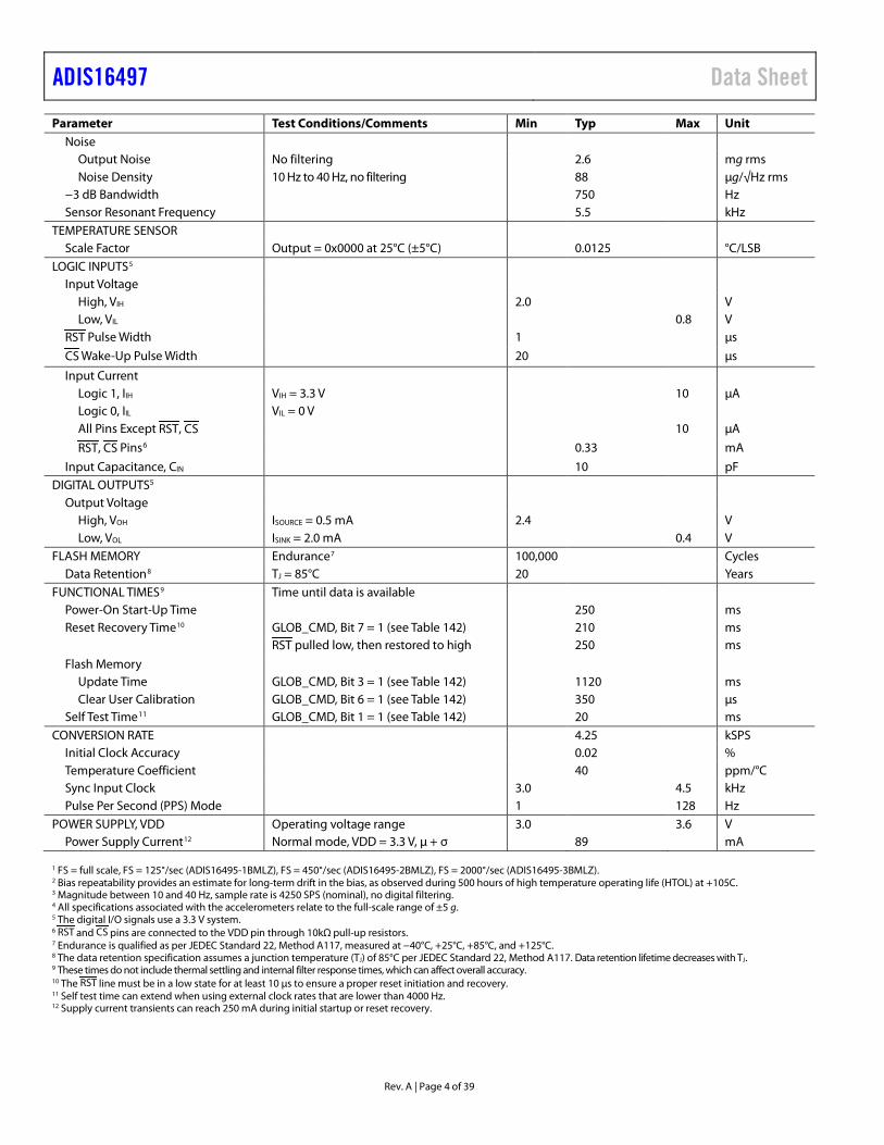
Parameter Test Conditions/Comments Min Typ Max Unit Noise
Output Noise No filtering 2.6 mg rms Noise Density 10 Hz to 40 Hz, no filtering 88 μg/√Hz rms
−3 dB Bandwidth 750 Hz Sensor Resonant Frequency 5.5 kHz
TEMPERATURE SENSOR Scale Factor Output = 0x0000 at 25°C (±5°C) 0.0125 °C/LSB
LOGIC INPUTS5 Input Voltage
High, VIH 2.0 V Low, VIL 0.8 V
RST Pulse Width 1 µs
CS Wake-Up Pulse Width 20 µs
Input Current Logic 1, IIH VIH = 3.3 V 10 µA Logic 0, IIL VIL = 0 V All Pins Except RST, CS 10 µA
RST, CS Pins6 0.33 mA
Input Capacitance, CIN 10 pF DIGITAL OUTPUTS5
Output Voltage High, VOH ISOURCE = 0.5 mA 2.4 V Low, VOL ISINK = 2.0 mA 0.4 V
FLASH MEMORY Endurance7 100,000 Cycles Data Retention8 TJ = 85°C 20 Years
FUNCTIONAL TIMES9 Time until data is available Power-On Start-Up Time 250 ms Reset Recovery Time10 GLOB_CMD, Bit 7 = 1 (see Table 142) 210 ms
RST pulled low, then restored to high 250 ms
Flash Memory Update Time GLOB_CMD, Bit 3 = 1 (see Table 142) 1120 ms Clear User Calibration GLOB_CMD, Bit 6 = 1 (see Table 142) 350 µs
Self Test Time11 GLOB_CMD, Bit 1 = 1 (see Table 142) 20 ms CONVERSION RATE 4.25 kSPS
Initial Clock Accuracy 0.02 % Temperature Coefficient 40 ppm/°C Sync Input Clock 3.0 4.5 kHz Pulse Per Second (PPS) Mode 1 128 Hz
POWER SUPPLY, VDD Operating voltage range 3.0 3.6 V Power Supply Current12 Normal mode, VDD = 3.3 V, µ + σ 89 mA
1 FS = full scale, FS = 125°/sec (ADIS16495-1BMLZ), FS = 450°/sec (ADIS16495-2BMLZ), FS = 2000°/sec (ADIS16495-3BMLZ). 2 Bias repeatability provides an estimate for long-term drift in the bias, as observed during 500 hours of high temperature operating life (HTOL) at +105C. 3 Magnitude between 10 and 40 Hz, sample rate is 4250 SPS (nominal), no digital filtering. 4 All specifications associated with the accelerometers relate to the full-scale range of ±5 g. 5 The digital I/O signals use a 3.3 V system. 6 RST and CS pins are connected to the VDD pin through 10kΩ pull-up resistors. 7 Endurance is qualified as per JEDEC Standard 22, Method A117, measured at −40°C, +25°C, +85°C, and +125°C. 8 The data retention specification assumes a junction temperature (TJ) of 85°C per JEDEC Standard 22, Method A117. Data retention lifetime decreases with TJ. 9 These times do not include thermal settling and internal filter response times, which can affect overall accuracy. 10 The RST line must be in a low state for at least 10 μs to ensure a proper reset initiation and recovery. 11 Self test time can extend when using external clock rates that are lower than 4000 Hz. 12 Supply current transients can reach 250 mA during initial startup or reset recovery.
Data Sheet ADIS16497
Rev. A | Page 5 of 39
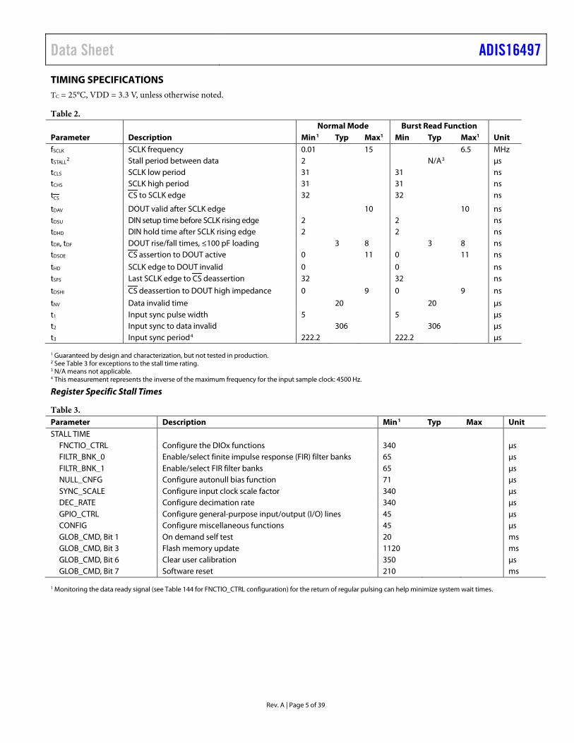
TIMING SPECIFICATIONS TC = 25°C, VDD = 3.3 V, unless otherwise noted.
Table 2. Normal Mode Burst Read Function
Parameter Description Min1 Typ Max1 Min Typ Max1 Unit fSCLK SCLK frequency 0.01 15 6.5 MHz tSTALL
2 Stall period between data 2 N/A3 µs tCLS SCLK low period 31 31 ns tCHS SCLK high period 31 31 ns tCS CS to SCLK edge 32 32 ns
tDAV DOUT valid after SCLK edge 10 10 ns tDSU DIN setup time before SCLK rising edge 2 2 ns tDHD DIN hold time after SCLK rising edge 2 2 ns tDR, tDF DOUT rise/fall times, ≤100 pF loading 3 8 3 8 ns tDSOE CS assertion to DOUT active 0 11 0 11 ns
tHD SCLK edge to DOUT invalid 0 0 ns tSFS Last SCLK edge to CS deassertion 32 32 ns
tDSHI CS deassertion to DOUT high impedance 0 9 0 9 ns
tNV Data invalid time 20 20 µs t1 Input sync pulse width 5 5 µs t2 Input sync to data invalid 306 306 µs t3 Input sync period4 222.2 222.2 µs
1 Guaranteed by design and characterization, but not tested in production. 2 See Table 3 for exceptions to the stall time rating. 3 N/A means not applicable. 4 This measurement represents the inverse of the maximum frequency for the input sample clock: 4500 Hz.
Register Specific Stall Times
Table 3. Parameter Description Min1 Typ Max Unit STALL TIME
FNCTIO_CTRL Configure the DIOx functions 340 μs FILTR_BNK_0 Enable/select finite impulse response (FIR) filter banks 65 μs FILTR_BNK_1 Enable/select FIR filter banks 65 μs NULL_CNFG Configure autonull bias function 71 μs SYNC_SCALE Configure input clock scale factor 340 μs DEC_RATE Configure decimation rate 340 μs GPIO_CTRL Configure general-purpose input/output (I/O) lines 45 μs CONFIG Configure miscellaneous functions 45 μs GLOB_CMD, Bit 1 On demand self test 20 ms GLOB_CMD, Bit 3 Flash memory update 1120 ms GLOB_CMD, Bit 6 Clear user calibration 350 μs GLOB_CMD, Bit 7 Software reset 210 ms
1 Monitoring the data ready signal (see Table 144 for FNCTIO_CTRL configuration) for the return of regular pulsing can help minimize system wait times.
ADIS16497 Data Sheet
Rev. A | Page 6 of 39
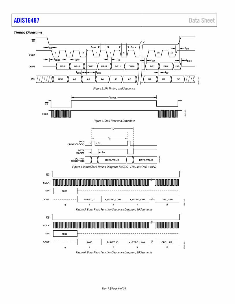
Timing Diagrams
CS
SCLK
DOUT
DIN
1 2 3 4 5 6 15 16
R/W A5A6 A4 A3 A2 D2
MSB DB14
D1 LSB
DB13 DB12 DB10DB11 DB2 LSBDB1
tCS
tDSHItDR
tSFS
tDF
tDAV tHD
tCHS tCLS
tDSOE
tDHDtDSU
1506
1-00
2
Figure 2. SPI Timing and Sequence
CS
SCLK
tSTALL
1506
1-00
3
Figure 3. Stall Time and Data Rate
t1
t2
t3
tNV
DIO4(SYNC CLOCK)
DATAREADY
OUTPUTREGISTERS DATA VALID DATA VALID
1506
1-00
4
Figure 4. Input Clock Timing Diagram, FNCTIO_CTRL, Bits[7:4] = 0xFD
7C00
BURST_ID X_GYRO_LOW X_GYRO_OUT CRC_UPR
0 1 2 3 18
CS
SCLK
DIN
DOUT
1506
1-00
5
Figure 5. Burst Read Function Sequence Diagram, 19 Segments
7C00
0000 BURST_ID X_GYRO_LOW CRC_UPR
0 1 2 3 19
CS
SCLK
DIN
DOUT
1506
1-00
6
Figure 6. Burst Read Function Sequence Diagram, 20 Segments
Data Sheet ADIS16497
Rev. A | Page 7 of 39
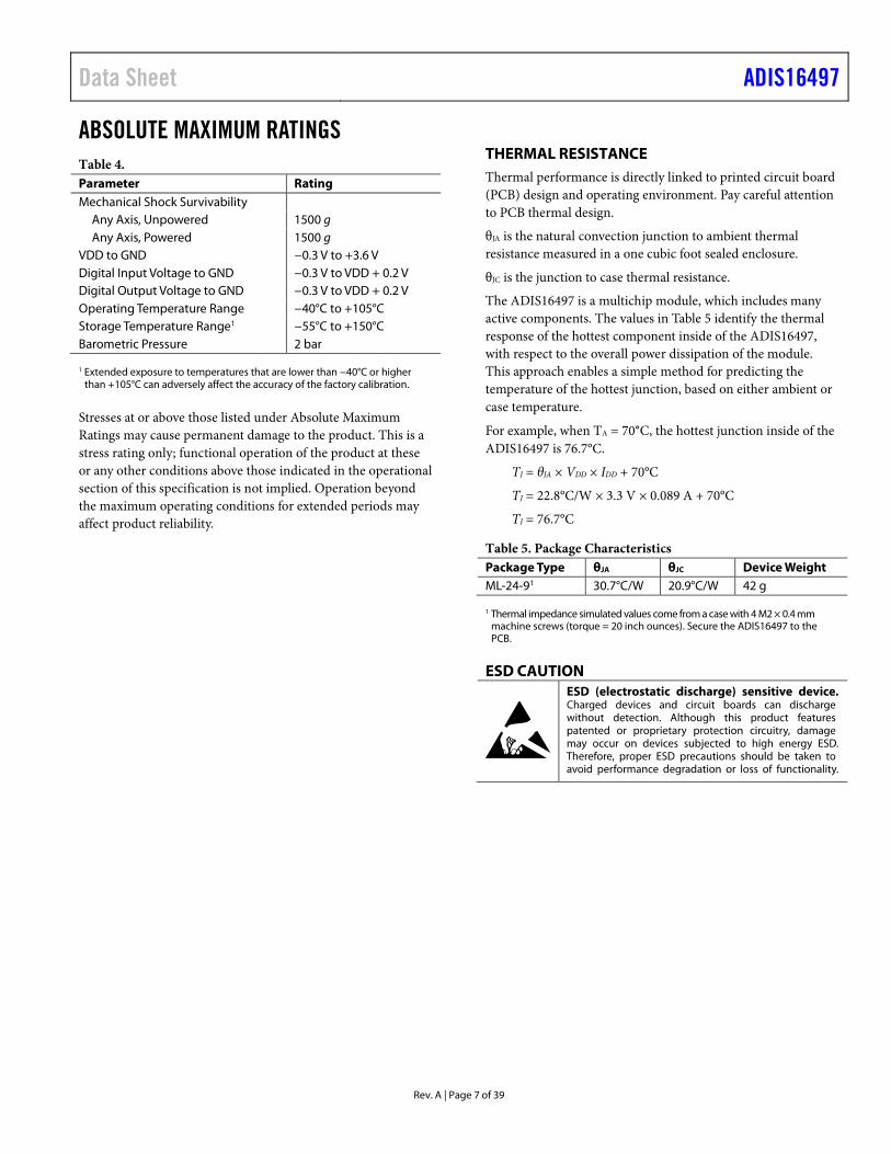
ABSOLUTE MAXIMUM RATINGS Table 4. Parameter Rating Mechanical Shock Survivability
Any Axis, Unpowered 1500 g Any Axis, Powered 1500 g
VDD to GND −0.3 V to +3.6 V Digital Input Voltage to GND −0.3 V to VDD + 0.2 V Digital Output Voltage to GND −0.3 V to VDD + 0.2 V Operating Temperature Range −40°C to +105°C Storage Temperature Range1 −55°C to +150°CBarometric Pressure 2 bar
1 Extended exposure to temperatures that are lower than −40°C or higher than +105°C can adversely affect the accuracy of the factory calibration.
Stresses at or above those listed under Absolute Maximum Ratings may cause permanent damage to the product. This is a stress rating only; functional operation of the product at these or any other conditions above those indicated in the operational section of this specification is not implied. Operation beyond the maximum operating conditions for extended periods may affect product reliability.
THERMAL RESISTANCE Thermal performance is directly linked to printed circuit board (PCB) design and operating environment. Pay careful attention to PCB thermal design.
θJA is the natural convection junction to ambient thermal resistance measured in a one cubic foot sealed enclosure.
θJC is the junction to case thermal resistance.
The ADIS16497 is a multichip module, which includes many active components. The values in Table 5 identify the thermal response of the hottest component inside of the ADIS16497, with respect to the overall power dissipation of the module. This approach enables a simple method for predicting the temperature of the hottest junction, based on either ambient or case temperature.
For example, when TA = 70°C, the hottest junction inside of the ADIS16497 is 76.7°C.
TJ = θJA × VDD × IDD + 70°C
TJ = 22.8°C/W × 3.3 V × 0.089 A + 70°C
TJ = 76.7°C
Table 5. Package Characteristics Package Type θJA θJC Device Weight ML-24-91 30.7°C/W 20.9°C/W 42 g
1 Thermal impedance simulated values come from a case with 4 M2 × 0.4 mm machine screws (torque = 20 inch ounces). Secure the ADIS16497 to the PCB.
ESD CAUTION

ADIS16497 Data Sheet
Rev. A | Page 8 of 39
PIN CONFIGURATION AND FUNCTION DESCRIPTIONS
1
DIO
3
SCLKDIN
DIO
1
DIO
2
VDD
GN
D
NO
PIN
DN
C
DN
C
DN
C
DN
C
DIO
4
DO
UT
CS
RST
VDD
NO
PIN
GN
D
DN
C
DN
C
DN
C
DN
C
DN
C
2
3
4
5
6
7
8
9
10
11
12
13
14
15
16
17
18
19
20
21
22
23
24
ADIS16497TOP VIEW
(Not to Scale)
NOTES1. THIS REPRESENTATION DISPLAYS THE TOP VIEW PINOUT FOR THE MATING SOCKET CONNECTOR.2. THE ACTUAL CONNECTOR PINS ARE NOT VISIBLE FROM THE TOP VIEW.3. MATING CONNECTOR: SAMTEC CLM-112-02 OR EQUIVALENT.4. DNC = DO NOT CONNECT.5. PIN 12 AND PIN 15 ARE NOT PHYSICALLY PRESENT. 15
061-
007
Figure 7. Pin Configuration
PIN 1PIN 23
PIN 1 PIN 2 1506
1-00
8
Figure 8. Axial Orientation (Top Side Facing Up)
Table 6. Pin Function Descriptions Pin No. Mnemonic Type Description 1 DIO3 Input/output Configurable Digital Input/Output 3. 2 DIO4 Input/output Configurable Digital Input/Output 4. 3 SCLK Input SPI Serial Clock. 4 DOUT Output SPI Data Output. Clocks output on the SCLK falling edge. 5 DIN Input SPI Data Input. Clocks input on the SCLK rising edge. 6 CS Input SPI Chip Select.
7 DIO1 Input/output Configurable Digital Input/Output 1. 8 RST Input Reset.
9 DIO2 Input/output Configurable Digital Input/Output 2. 10, 11 VDD Supply Power Supply. 12, 15 NO PIN Not applicable No Pin. These pins are not physically present. 13, 14 GND Supply Power Ground. 16 to 24 DNC Not applicable Do Not Connect. Do not connect to these pins.
Data Sheet ADIS16497
Rev. A | Page 9 of 39
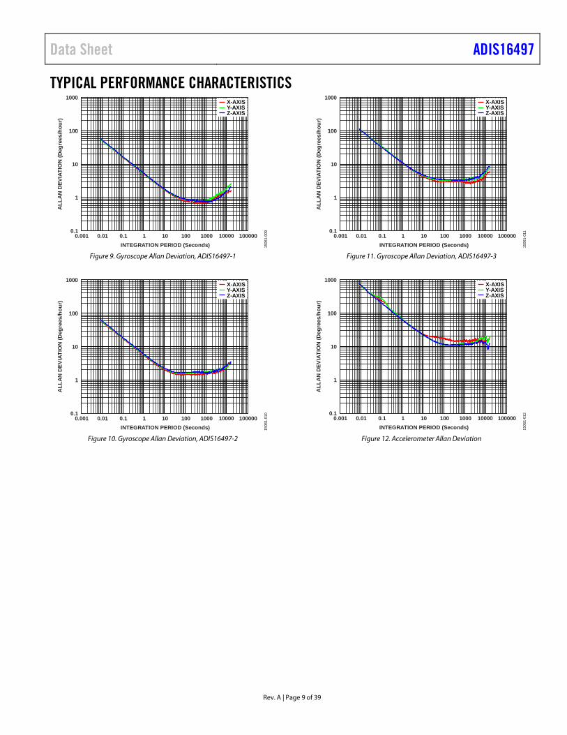
TYPICAL PERFORMANCE CHARACTERISTICS
0.001 0.01 0.1 1 10 100 1000 10000 100000INTEGRATION PERIOD (Seconds)
0.1
1
10
100
1000
ALL
AN
DEV
IATI
ON
(Deg
rees
/hou
r)
X-AXISY-AXISZ-AXIS
1506
1-00
9
Figure 9. Gyroscope Allan Deviation, ADIS16497-1
0.001 0.01 0.1 1 10 100 1000 10000 100000INTEGRATION PERIOD (Seconds)
0.1
1
10
100
1000
ALL
AN
DEV
IATI
ON
(Deg
rees
/hou
r)
X-AXISY-AXISZ-AXIS
1506
1-01
0
Figure 10. Gyroscope Allan Deviation, ADIS16497-2
0.001 0.01 0.1 1 10 100 1000 10000 100000INTEGRATION PERIOD (Seconds)
0.1
1
10
100
1000
ALL
AN
DEV
IATI
ON
(Deg
rees
/hou
r)
X-AXISY-AXISZ-AXIS
1506
1-01
1
Figure 11. Gyroscope Allan Deviation, ADIS16497-3
0.001 0.01 0.1 1 10 100 1000 10000 100000INTEGRATION PERIOD (Seconds)
0.1
1
10
100
1000
ALL
AN
DEV
IATI
ON
(Deg
rees
/hou
r)
X-AXISY-AXISZ-AXIS
1506
1-01
2
Figure 12. Accelerometer Allan Deviation
ADIS16497 Data Sheet
Rev. A | Page 10 of 39
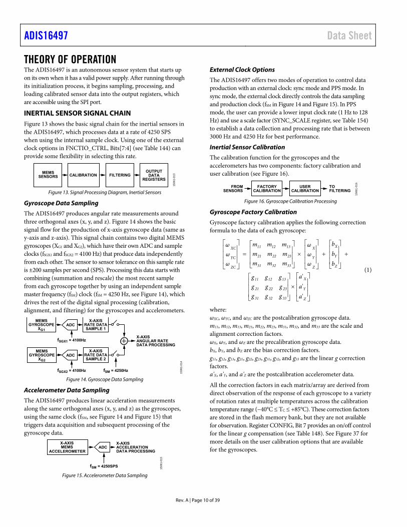
THEORY OF OPERATION The ADIS16497 is an autonomous sensor system that starts up on its own when it has a valid power supply. After running through its initialization process, it begins sampling, processing, and loading calibrated sensor data into the output registers, which are accessible using the SPI port.
INERTIAL SENSOR SIGNAL CHAIN Figure 13 shows the basic signal chain for the inertial sensors in the ADIS16497, which processes data at a rate of 4250 SPS when using the internal sample clock. Using one of the external clock options in FNCTIO_CTRL, Bits[7:4] (see Table 144) can provide some flexibility in selecting this rate.
MEMSSENSORS CALIBRATION FILTERING
OUTPUTDATA
REGISTERS
1506
1-01
3
Figure 13. Signal Processing Diagram, Inertial Sensors
Gyroscope Data Sampling
The ADIS16497 produces angular rate measurements around three orthogonal axes (x, y, and z). Figure 14 shows the basic signal flow for the production of x-axis gyroscope data (same as y-axis and z-axis). This signal chain contains two digital MEMS gyroscopes (XG1 and XG2), which have their own ADC and sample clocks (fSGX1 and fSGX2 = 4100 Hz) that produce data independently from each other. The sensor to sensor tolerance on this sample rate is ±200 samples per second (SPS). Processing this data starts with combining (summation and rescale) the most recent sample from each gyroscope together by using an independent sample master frequency (fSM) clock (fSM = 4250 Hz, see Figure 14), which drives the rest of the digital signal processing (calibration, alignment, and filtering) for the gyroscopes and accelerometers.
MEMSGYROSCOPE
XG1
MEMSGYROSCOPE
XG2
X-AXISRATE DATASAMPLE 1
X-AXISANGULAR RATEDATA PROCESSING
fSM = 4250Hz
X-AXISRATE DATASAMPLE 2
fSGX2 = 4100Hz
fSGX1 = 4100Hz
ADC
ADC
1506
1-01
4
Figure 14. Gyroscope Data Sampling
Accelerometer Data Sampling
The ADIS16497 produces linear acceleration measurements along the same orthogonal axes (x, y, and z) as the gyroscopes, using the same clock (fSM, see Figure 14 and Figure 15) that triggers data acquisition and subsequent processing of the gyroscope data.
ACCELEROMETER
X-AXISMEMS
X-AXISACCELERATIONDATA PROCESSING
fSM = 4250SPS
ADC
1506
1-01
5
Figure 15. Accelerometer Data Sampling
External Clock Options
The ADIS16497 offers two modes of operation to control data production with an external clock: sync mode and PPS mode. In sync mode, the external clock directly controls the data sampling and production clock (fSM in Figure 14 and Figure 15). In PPS mode, the user can provide a lower input clock rate (1 Hz to 128 Hz) and use a scale factor (SYNC_SCALE register, see Table 154) to establish a data collection and processing rate that is between 3000 Hz and 4250 Hz for best performance.
Inertial Sensor Calibration
The calibration function for the gyroscopes and the accelerometers has two components: factory calibration and user calibration (see Figure 16).
FROMSENSORS
TOFILTERING
FACTORYCALIBRATION
USERCALIBRATION
1506
1-01
6
Figure 16. Gyroscope Calibration Processing
Gyroscope Factory Calibration
Gyroscope factory calibration applies the following correction formula to the data of each gyroscope:
Z
Y
X
333231
232221
131211
Z
Y
X
Z
Y
X
333231
232221
131211
ZC
YC
XC
aaa
ggggggggg
bbb
ωωω
mmmmmmmmm
ωωω
'''
(1)
where: ωXC, ωYC, and ωZC are the postcalibration gyroscope data. m11, m12, m13, m21, m22, m23, m31, m32, and m33 are the scale and alignment correction factors. ωX, ωY, and ωZ are the precalibration gyroscope data. bX, bY, and bZ are the bias correction factors. g11, g12, g13, g21, g22, g23, g31, g32, and g33 are the linear g correction factors. a'X, a'Y, and a'Z are the postcalibration accelerometer data.
All the correction factors in each matrix/array are derived from direct observation of the response of each gyroscope to a variety of rotation rates at multiple temperatures across the calibration temperature range (−40°C ≤ TC ≤ +85°C). These correction factors are stored in the flash memory bank, but they are not available for observation. Register CONFIG, Bit 7 provides an on/off control for the linear g compensation (see Table 148). See Figure 37 for more details on the user calibration options that are available for the gyroscopes.
Data Sheet ADIS16497
Rev. A | Page 11 of 39
Accelerometer Factory Calibration
The accelerometer factory calibration applies the following correction formulas to the data of each accelerometer:
2
2
2
00
0
'''
ZC
YC
XC
3231
2321
1312
Z
Y
X
Z
Y
X
333231
232221
131211
Z
Y
X
pppppp
bbb
aaa
mmmmmmmmm
aaa
(2)
where: a'X, a'Y, and a'Z are the postcalibration accelerometer data. m11, m12, m13, m21, m22, m23, m31, m32, and m33 are the scale and alignment correction factors. aX, aY, and aZ are the precalibration accelerometer data. bX, bY, and bZ are the bias correction factors. 0, p12, p13, p21, p23, p31, and p32 are the point of percussion correction factors ω2
XC, ω2YC, and ω2
ZC are the postcalibration gyroscope data (squared).
All the correction factors in each matrix/array are derived from direct observation of the response of each accelerometer to a variety of inertial test conditions at multiple temperatures across the calibration temperature range (−40°C ≤ TC ≤ +85°C). These correction factors are stored in the flash memory bank, but they are not available for observation. Register CONFIG, Bit 6 provides an on/off control for the point of percussion alignment (see Table 148). See Figure 38 for more details on the user calibration options that are available for the accelerometers.
Filtering
After calibration, the data of each inertial sensor passes through two digital filters, both of which have user configurable attributes: FIR and decimation (see Figure 17).
FROMCALIBRATION
TODATAREGISTERS
FIRFILTER
DECIMATIONFILTER
1506
1-01
7
Figure 17. Inertial Sensor Filtering
The FIR filter includes four banks of coefficients that have 120 taps each. Register FILTR_BNK_0 (see Table 158) and Register FILTR_BNK_1 (see Table 160) provide the configuration options for the use of the FIR filters of each inertial sensor. Each FIR filter bank includes a preconfigured filter, but the user can design their own filters and write over these values using the register of each coefficient. For example, Table 163 provides the details for the FIR_COEF_A071 register, which contains Coefficient 71 in FIR Bank A. Refer to Figure 41 for the frequency response of the factory default filters. These filters do not represent any specific application environment; they are only examples.
The decimation filter averages multiple samples together to produce each register update. In this type of filter structure, the number of samples in the average is equal to the reduction in the update rate for the output data registers. See the DEC_RATE regis-ter for the user controls for this filter (see Table 150).
REGISTER STRUCTURE All communication with the ADIS16497 involves accessing its user registers. The register structure contains both output data and control registers. The output data registers include the latest sensor data, error flags, and identification data. The control registers include sample rate, filtering, I/O, calibration, and diagnostic configuration options. All communication between the ADIS16497 and an external processor involves either reading or writing to one of the user registers.
TRIAXIALGYROSCOPE
TEMPERATURESENSOR
TRIAXIALACCELEROMETER
DSPADC OUTPUTREGISTERS
CONTROLREGISTERSCONTROLLER
SP
I
1506
1-01
8
Figure 18. Basic Operation
The register structure uses a paged addressing scheme that contains 13 pages, with each page containing 64 register locations. Each register is 16 bits wide, with each byte having its own unique address within the memory map of that page. The SPI port has access to one page at a time, using the bit sequence in Figure 19. Select the page to activate for SPI access by writing its code to the PAGE_ID register. Read the PAGE_ID register to determine which page is currently active. Table 7 displays the PAGE_ID contents for each page and their basic functions. The PAGE_ID register is located at Address 0x00 on every page.
Table 7. User Register Page Assignments Page PAGE_ID Function 0 0x00 Output data, clock, identification 1 0x01 Reserved 2 0x02 Calibration 3 0x03 Control: sample rate, filtering, I/O 4 0x04 Serial number, cyclic redundancy check (CRC)
values 5 0x05 FIR Filter Bank A, Coefficient 0 to Coefficient 59 6 0x06 FIR Filter Bank A, Coefficient 60 to Coefficient 119 7 0x07 FIR Filter Bank B, Coefficient 0 to Coefficient 59 8 0x08 FIR Filter Bank B, Coefficient 60 to Coefficient 119 9 0x09 FIR Filter Bank C, Coefficient 0 to Coefficient 59 10 0x0A FIR Filter Bank C, Coefficient 60 to Coefficient 119 11 0x0B FIR Filter Bank D, Coefficient 0 to Coefficient 59 12 0x0C FIR Filter Bank D, Coefficient 60 to Coefficient 119
ADIS16497 Data Sheet
Rev. A | Page 12 of 39
R/W R/WA6 A5 A4 A3 A2 A1 A0 DC7 DC6 DC5 DC4 DC3 DC2 DC1 DC0
D0D1D2D3D4D5D6D7D8D9D10D11D12D13D14D15
CS
SCLK
DIN
DOUT
A6 A5
D13D14D15
NOTES1. DOUT BITS ARE PRODUCED ONLY WHEN THE PREVIOUS 16-BIT DIN SEQUENCE STARTS WITH R/W = 0.2. WHEN CS IS HIGH, DOUT IS IN A THREE-STATE, HIGH IMPEDANCE MODE, WHICH ALLOWS MULTIFUNCTIONAL USE OF THE LINE
FOR OTHER DEVICES. 1506
1-01
9
Figure 19. SPI Communication Bit Sequence
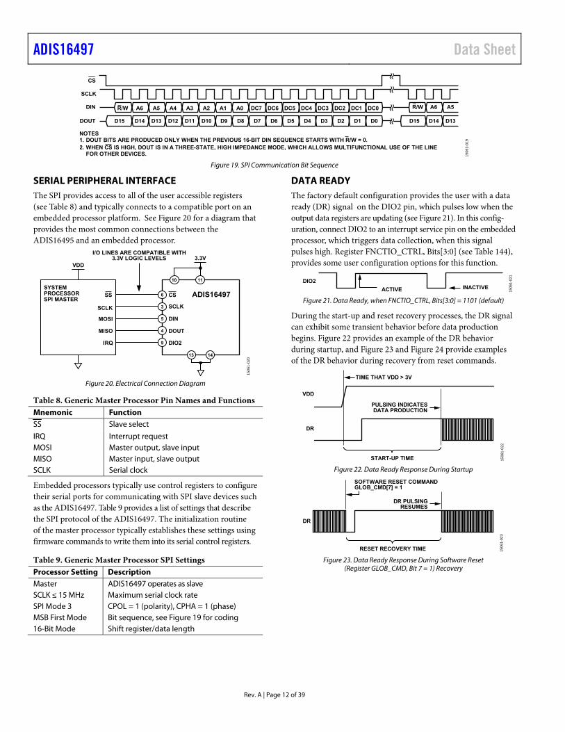
SERIAL PERIPHERAL INTERFACE The SPI provides access to all of the user accessible registers (see Table 8) and typically connects to a compatible port on an embedded processor platform. See Figure 20 for a diagram that provides the most common connections between the ADIS16495 and an embedded processor.
SYSTEMPROCESSORSPI MASTER
SCLK
CS
DIN
DOUT
SCLK
SS
MOSI
MISO
3.3V
IRQ DIO2
VDD
I/O LINES ARE COMPATIBLE WITH3.3V LOGIC LEVELS
10
6
3
5
4
9
11
13 14
ADIS16497
1506
1-02
0
Figure 20. Electrical Connection Diagram
Table 8. Generic Master Processor Pin Names and Functions Mnemonic FunctionSS Slave select
IRQ Interrupt requestMOSI Master output, slave input MISO Master input, slave output SCLK Serial clock
Embedded processors typically use control registers to configure their serial ports for communicating with SPI slave devices such as the ADIS16497. Table 9 provides a list of settings that describe the SPI protocol of the ADIS16497. The initialization routine of the master processor typically establishes these settings using firmware commands to write them into its serial control registers.
Table 9. Generic Master Processor SPI Settings Processor Setting Description Master ADIS16497 operates as slave SCLK ≤ 15 MHz Maximum serial clock rate SPI Mode 3 CPOL = 1 (polarity), CPHA = 1 (phase) MSB First Mode Bit sequence, see Figure 19 for coding 16-Bit Mode Shift register/data length
DATA READY The factory default configuration provides the user with a data ready (DR) signal on the DIO2 pin, which pulses low when the output data registers are updating (see Figure 21). In this config-uration, connect DIO2 to an interrupt service pin on the embedded processor, which triggers data collection, when this signal pulses high. Register FNCTIO_CTRL, Bits[3:0] (see Table 144), provides some user configuration options for this function.
DIO2
ACTIVE INACTIVE
1506
1-02
1
Figure 21. Data Ready, when FNCTIO_CTRL, Bits[3:0] = 1101 (default)
During the start-up and reset recovery processes, the DR signal can exhibit some transient behavior before data production begins. Figure 22 provides an example of the DR behavior during startup, and Figure 23 and Figure 24 provide examples of the DR behavior during recovery from reset commands.
VDD
DR
START-UP TIME
TIME THAT VDD > 3V
PULSING INDICATESDATA PRODUCTION
1506
1-02
2
Figure 22. Data Ready Response During Startup
DR
RESET RECOVERY TIME
SOFTWARE RESET COMMANDGLOB_CMD[7] = 1
DR PULSINGRESUMES
1506
1-02
3
Figure 23. Data Ready Response During Software Reset (Register GLOB_CMD, Bit 7 = 1) Recovery
Data Sheet ADIS16497
Rev. A | Page 13 of 39
DR
RST
RESET RECOVERY TIME
RST PINRELEASED
DR PULSINGRESUMES
1506
1-02
4
Figure 24. Data Ready Response During Reset (RST = 0) Recovery
READING SENSOR DATA Reading a single register requires two 16-bit cycles on the SPI: one to request the contents of a register and another to receive those contents. The 16-bit command code (see Figure 19) for a read request on the SPI has three parts: the read bit (R/W = 0), the 7-bit address code for either address (upper or lower) of the register, Bits[A6:A0], and eight don’t care bits, Bits[DC7:DC0]. Figure 25 provides an example that includes two register reads in succession. This example starts with DIN = 0x1A00, to request the contents of the Z_GYRO_OUT register, and follows with 0x1800, to request the contents of the Z_GYRO_LOW register (assuming PAGE_ID already equals 0x0000). The sequence in Figure 25 also shows full duplex mode of operation, which means that the ADIS16497 can receive requests on DIN while also transmitting data out on DOUT within the same 16-bit SPI cycle.
DIN
DOUT
0x1A00 0x1800 NEXTADDRESS
Z_GYRO_OUT Z_GYRO_LOW
1506
1-02
5
Figure 25. SPI Read Example
Figure 26 provides an example of the four SPI signals when reading the PROD_ID register (see Table 92) in a repeating pattern. This pattern can be helpful when troubleshooting the SPI interface setup and communications.
SCLK
CS
DOUT
DIN
DOUT = 0100 0000 0111 0001 = 0x4071 = 16497 (PROD_ID)
DIN = 0111 1110 0000 0000 = 0x7E00
1506
1-02
6
Figure 26. SPI Read Example, Second 16-Bit Sequence
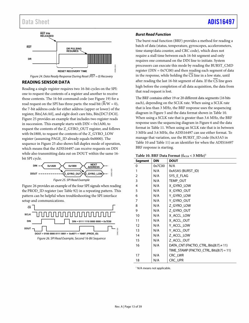
Burst Read Function
The burst read function (BRF) provides a method for reading a batch of data (status, temperature, gyroscopes, accelerometers, time stamp/data counter, and CRC code), which does not require a stall time between each 16-bit segment and only requires one command on the DIN line to initiate. System processors can execute this mode by reading the BURST_CMD register (DIN = 0x7C00) and then reading each segment of data in the response, while holding the CS line in a low state, until after reading the last 16-bit segment of data. If the CS line goes high before the completion of all data acquisition, the data from that read request is lost.
The BRF contains either 19 or 20 different data segments (16 bits each), depending on the SCLK rate. When using a SCLK rate that is less than 3 MHz, the BRF response uses the sequencing diagram in Figure 5 and the data format shown in Table 10. When using a SCLK rate that is greater than 3.6 MHz, the BRF response uses the sequencing diagram in Figure 6 and the data format in Table 11. When using an SCLK rate that is in between 3 MHz and 3.6 MHz, the ADIS16497 can use either format. To manage that variation, use the BURST_ID code (0xA5A5 in Table 10 and Table 11) as an identifier for when the ADIS16497 BRF response is starting.
Table 10. BRF Data Format (fSCLK < 3 MHz)1 Segment DIN DOUT
0 0x7C00 N/A1 N/A 0xA5A5 (BURST_ID)2 N/A SYS_E_FLAG3 N/A TEMP_OUT4 N/A X_GYRO_LOW5 N/A X_GYRO_OUT6 N/A Y_GYRO_LOW7 N/A Y_GYRO_OUT8 N/A Z_GYRO_LOW9 N/A Z_GYRO_OUT10 N/A X_ACCL_LOW11 N/A X_ACCL_OUT12 N/A Y_ACCL_LOW13 N/A Y_ACCL_OUT14 N/A Z_ACCL_LOW15 N/A Z_ACCL_OUT16 N/A DATA_CNT (FNCTIO_CTRL, Bits[8:7] ≠ 11)
TIME_STAMP (FNCTIO_CTRL, Bits[8:7] = 11) 17 N/A CRC_LWR18 N/A CRC_UPR
1 N/A means not applicable.

ADIS16497 Data Sheet
Rev. A | Page 14 of 39
Table 11. BRF Data Format (fSCLK > 3.6 MHz)1 Segment DIN DOUT
0 0x7C00 N/A1 N/A 0x00002 N/A 0xA5A5 (BURST_ID)3 N/A SYS_E_FLAG4 N/A TEMP_OUT5 N/A X_GYRO_LOW6 N/A X_GYRO_OUT7 N/A Y_GYRO_LOW8 N/A Y_GYRO_OUT9 N/A Z_GYRO_LOW10 N/A Z_GYRO_OUT11 N/A X_ACCL_LOW12 N/A X_ACCL_OUT13 N/A Y_ACCL_LOW14 N/A Y_ACCL_OUT15 N/A Z_ACCL_LOW16 N/A Z_ACCL_OUT17 N/A DATA_CNT (FNCTIO_CTRL, Bits[8:7] ≠ 11)
TIME_STAMP (FNCTIO_CTRL, Bits[8:7] = 11) 18 N/A CRC_LWR19 N/A CRC_UPR
1 N/A means not applicable.
DEVICE CONFIGURATION Each register contains 16 bits (two bytes); Bits[7:0] contain the low byte and Bits[15:8] contain the high byte. Each byte has its own unique address in the user register map (see Table 12). Updating the contents of a register requires writing to its low byte first and its high byte second. There are three parts to coding a SPI command (see Figure 19), which writes a new byte of data to a register: the write bit (R/W = 1), the 7-bit address code for the byte that this command is updating, and the new data for that location, Bits[DC7:DC0]. Figure 27 provides a coding example for writing 0xFEDC to the XG_BIAS_LOW register (see Table 106), assuming PAGE_ID already equals 0x0002.
SCLK
CS
DIN 0x90DC 0x91FE
1506
1-02
7
Figure 27. SPI Sequence for Writing 0xFEDC to XG_BIAS_LOW
Dual Memory Structure
The ADIS16497 uses a dual memory structure (see Figure 28), with static random access memory (SRAM) supporting real-time operation and flash memory storing operational code, calibration coefficients, and user configurable register settings. The manual flash update command (GLOB_CMD, Bit 3, see Table 142) provides a single-command method for storing user configuration settings into flash memory, for automatic recall during the next power-on or reset recovery process. This portion of the flash memory bank has two independent banks that operate in a ping pong manner, alternating with every flash update. During power-on or reset recovery, the ADIS16497 performs a CRC on the SRAM and compares it to a CRC computation from the same memory locations in flash memory. If this memory test fails fails, the ADIS16497 resets and boots up from the other flash memory location. SYS_E_FLAG, Bit 2 (see Table 18) provides an error flag for detecting when the backup flash memory supported the last power-on or reset recovery. Table 12 provides a memory map for the user registers in the ADIS16497, which includes flash backup support (indicated by yes or no in the flash column).
NONVOLATILEFLASH MEMORY
(NO SPI ACCESS)
MANUALFLASH
BACKUP
START-UPRESET
VOLATILESRAM
SPI ACCESS
1506
1-02
8
Figure 28. SRAM and Flash Memory Diagram
Data Sheet ADIS16497
Rev. A | Page 15 of 39
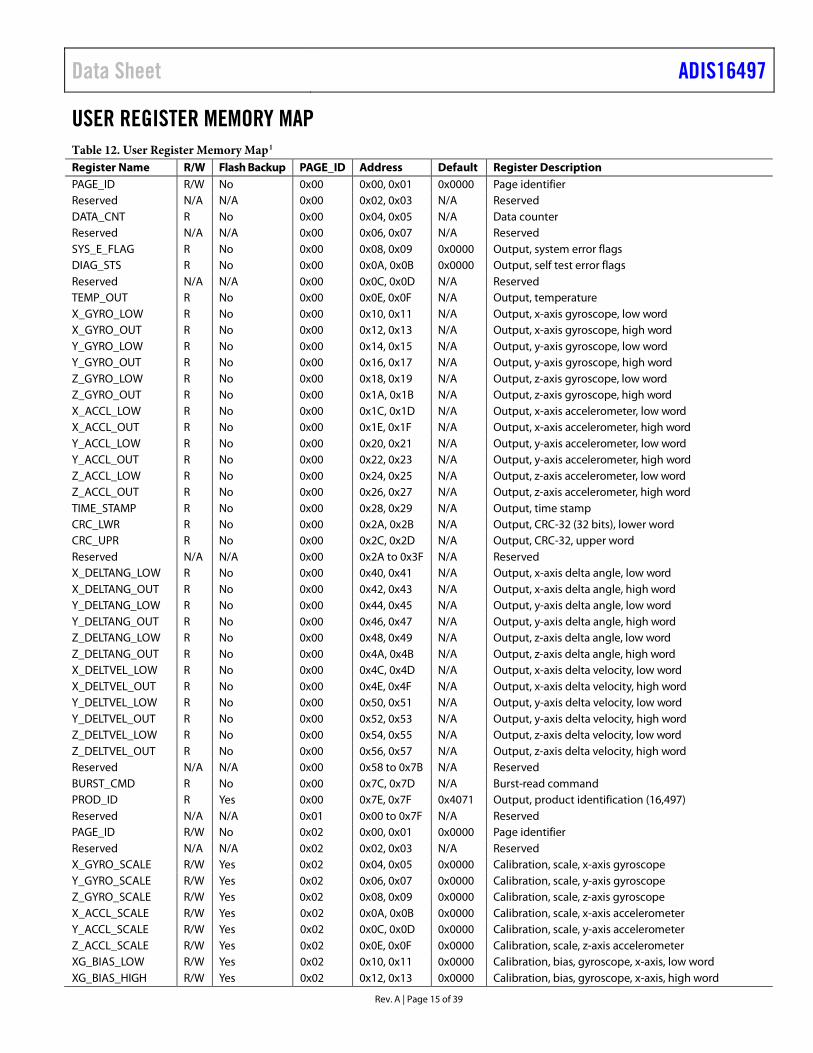
USER REGISTER MEMORY MAP Table 12. User Register Memory Map1 Register Name R/W Flash Backup PAGE_ID Address Default Register Description PAGE_ID R/W No 0x00 0x00, 0x01 0x0000 Page identifier Reserved N/A N/A 0x00 0x02, 0x03 N/A Reserved DATA_CNT R No 0x00 0x04, 0x05 N/A Data counter Reserved N/A N/A 0x00 0x06, 0x07 N/A Reserved SYS_E_FLAG R No 0x00 0x08, 0x09 0x0000 Output, system error flags DIAG_STS R No 0x00 0x0A, 0x0B 0x0000 Output, self test error flags Reserved N/A N/A 0x00 0x0C, 0x0D N/A Reserved TEMP_OUT R No 0x00 0x0E, 0x0F N/A Output, temperature X_GYRO_LOW R No 0x00 0x10, 0x11 N/A Output, x-axis gyroscope, low word X_GYRO_OUT R No 0x00 0x12, 0x13 N/A Output, x-axis gyroscope, high word Y_GYRO_LOW R No 0x00 0x14, 0x15 N/A Output, y-axis gyroscope, low word Y_GYRO_OUT R No 0x00 0x16, 0x17 N/A Output, y-axis gyroscope, high word Z_GYRO_LOW R No 0x00 0x18, 0x19 N/A Output, z-axis gyroscope, low word Z_GYRO_OUT R No 0x00 0x1A, 0x1B N/A Output, z-axis gyroscope, high word X_ACCL_LOW R No 0x00 0x1C, 0x1D N/A Output, x-axis accelerometer, low word X_ACCL_OUT R No 0x00 0x1E, 0x1F N/A Output, x-axis accelerometer, high word Y_ACCL_LOW R No 0x00 0x20, 0x21 N/A Output, y-axis accelerometer, low word Y_ACCL_OUT R No 0x00 0x22, 0x23 N/A Output, y-axis accelerometer, high word Z_ACCL_LOW R No 0x00 0x24, 0x25 N/A Output, z-axis accelerometer, low word Z_ACCL_OUT R No 0x00 0x26, 0x27 N/A Output, z-axis accelerometer, high word TIME_STAMP R No 0x00 0x28, 0x29 N/A Output, time stamp CRC_LWR R No 0x00 0x2A, 0x2B N/A Output, CRC-32 (32 bits), lower word CRC_UPR R No 0x00 0x2C, 0x2D N/A Output, CRC-32, upper word Reserved N/A N/A 0x00 0x2A to 0x3F N/A Reserved X_DELTANG_LOW R No 0x00 0x40, 0x41 N/A Output, x-axis delta angle, low word X_DELTANG_OUT R No 0x00 0x42, 0x43 N/A Output, x-axis delta angle, high word Y_DELTANG_LOW R No 0x00 0x44, 0x45 N/A Output, y-axis delta angle, low word Y_DELTANG_OUT R No 0x00 0x46, 0x47 N/A Output, y-axis delta angle, high word Z_DELTANG_LOW R No 0x00 0x48, 0x49 N/A Output, z-axis delta angle, low word Z_DELTANG_OUT R No 0x00 0x4A, 0x4B N/A Output, z-axis delta angle, high word X_DELTVEL_LOW R No 0x00 0x4C, 0x4D N/A Output, x-axis delta velocity, low word X_DELTVEL_OUT R No 0x00 0x4E, 0x4F N/A Output, x-axis delta velocity, high word Y_DELTVEL_LOW R No 0x00 0x50, 0x51 N/A Output, y-axis delta velocity, low word Y_DELTVEL_OUT R No 0x00 0x52, 0x53 N/A Output, y-axis delta velocity, high word Z_DELTVEL_LOW R No 0x00 0x54, 0x55 N/A Output, z-axis delta velocity, low word Z_DELTVEL_OUT R No 0x00 0x56, 0x57 N/A Output, z-axis delta velocity, high word Reserved N/A N/A 0x00 0x58 to 0x7B N/A Reserved BURST_CMD R No 0x00 0x7C, 0x7D N/A Burst-read command PROD_ID R Yes 0x00 0x7E, 0x7F 0x4071 Output, product identification (16,497) Reserved N/A N/A 0x01 0x00 to 0x7F N/A Reserved PAGE_ID R/W No 0x02 0x00, 0x01 0x0000 Page identifier Reserved N/A N/A 0x02 0x02, 0x03 N/A Reserved X_GYRO_SCALE R/W Yes 0x02 0x04, 0x05 0x0000 Calibration, scale, x-axis gyroscope Y_GYRO_SCALE R/W Yes 0x02 0x06, 0x07 0x0000 Calibration, scale, y-axis gyroscope Z_GYRO_SCALE R/W Yes 0x02 0x08, 0x09 0x0000 Calibration, scale, z-axis gyroscope X_ACCL_SCALE R/W Yes 0x02 0x0A, 0x0B 0x0000 Calibration, scale, x-axis accelerometer Y_ACCL_SCALE R/W Yes 0x02 0x0C, 0x0D 0x0000 Calibration, scale, y-axis accelerometer Z_ACCL_SCALE R/W Yes 0x02 0x0E, 0x0F 0x0000 Calibration, scale, z-axis accelerometer XG_BIAS_LOW R/W Yes 0x02 0x10, 0x11 0x0000 Calibration, bias, gyroscope, x-axis, low word XG_BIAS_HIGH R/W Yes 0x02 0x12, 0x13 0x0000 Calibration, bias, gyroscope, x-axis, high word
ADIS16497 Data Sheet
Rev. A | Page 16 of 39
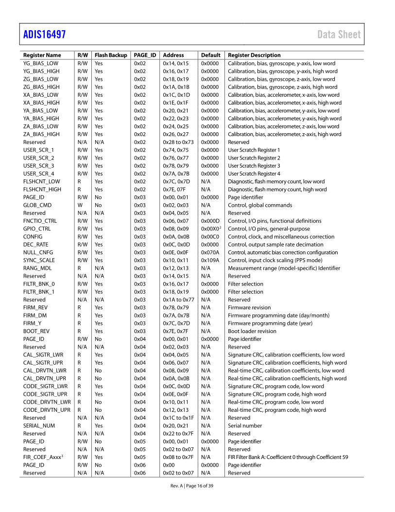
Register Name R/W Flash Backup PAGE_ID Address Default Register Description YG_BIAS_LOW R/W Yes 0x02 0x14, 0x15 0x0000 Calibration, bias, gyroscope, y-axis, low word YG_BIAS_HIGH R/W Yes 0x02 0x16, 0x17 0x0000 Calibration, bias, gyroscope, y-axis, high word ZG_BIAS_LOW R/W Yes 0x02 0x18, 0x19 0x0000 Calibration, bias, gyroscope, z-axis, low word ZG_BIAS_HIGH R/W Yes 0x02 0x1A, 0x1B 0x0000 Calibration, bias, gyroscope, z-axis, high word XA_BIAS_LOW R/W Yes 0x02 0x1C, 0x1D 0x0000 Calibration, bias, accelerometer, x-axis, low word XA_BIAS_HIGH R/W Yes 0x02 0x1E, 0x1F 0x0000 Calibration, bias, accelerometer, x-axis, high word YA_BIAS_LOW R/W Yes 0x02 0x20, 0x21 0x0000 Calibration, bias, accelerometer, y-axis, low word YA_BIAS_HIGH R/W Yes 0x02 0x22, 0x23 0x0000 Calibration, bias, accelerometer, y-axis, high word ZA_BIAS_LOW R/W Yes 0x02 0x24, 0x25 0x0000 Calibration, bias, accelerometer, z-axis, low word ZA_BIAS_HIGH R/W Yes 0x02 0x26, 0x27 0x0000 Calibration, bias, accelerometer, z-axis, high word Reserved N/A N/A 0x02 0x28 to 0x73 0x0000 Reserved USER_SCR_1 R/W Yes 0x02 0x74, 0x75 0x0000 User Scratch Register 1 USER_SCR_2 R/W Yes 0x02 0x76, 0x77 0x0000 User Scratch Register 2 USER_SCR_3 R/W Yes 0x02 0x78, 0x79 0x0000 User Scratch Register 3 USER_SCR_4 R/W Yes 0x02 0x7A, 0x7B 0x0000 User Scratch Register 4 FLSHCNT_LOW R Yes 0x02 0x7C, 0x7D N/A Diagnostic, flash memory count, low word FLSHCNT_HIGH R Yes 0x02 0x7E, 07F N/A Diagnostic, flash memory count, high word PAGE_ID R/W No 0x03 0x00, 0x01 0x0000 Page identifier GLOB_CMD W No 0x03 0x02, 0x03 N/A Control, global commands Reserved N/A N/A 0x03 0x04, 0x05 N/A Reserved FNCTIO_CTRL R/W Yes 0x03 0x06, 0x07 0x000D Control, I/O pins, functional definitions GPIO_CTRL R/W Yes 0x03 0x08, 0x09 0x00X02 Control, I/O pins, general-purpose CONFIG R/W Yes 0x03 0x0A, 0x0B 0x00C0 Control, clock, and miscellaneous correction DEC_RATE R/W Yes 0x03 0x0C, 0x0D 0x0000 Control, output sample rate decimation NULL_CNFG R/W Yes 0x03 0x0E, 0x0F 0x070A Control, automatic bias correction configuration SYNC_SCALE R/W Yes 0x03 0x10, 0x11 0x109A Control, input clock scaling (PPS mode) RANG_MDL R N/A 0x03 0x12, 0x13 N/A Measurement range (model-specific) Identifier Reserved N/A N/A 0x03 0x14, 0x15 N/A Reserved FILTR_BNK_0 R/W Yes 0x03 0x16, 0x17 0x0000 Filter selection FILTR_BNK_1 R/W Yes 0x03 0x18, 0x19 0x0000 Filter selection Reserved N/A N/A 0x03 0x1A to 0x77 N/A Reserved FIRM_REV R Yes 0x03 0x78, 0x79 N/A Firmware revision FIRM_DM R Yes 0x03 0x7A, 0x7B N/A Firmware programming date (day/month) FIRM_Y R Yes 0x03 0x7C, 0x7D N/A Firmware programming date (year) BOOT_REV R Yes 0x03 0x7E, 0x7F N/A Boot loader revision PAGE_ID R/W No 0x04 0x00, 0x01 0x0000 Page identifier Reserved N/A N/A 0x04 0x02, 0x03 N/A Reserved CAL_SIGTR_LWR R Yes 0x04 0x04, 0x05 N/A Signature CRC, calibration coefficients, low word CAL_SIGTR_UPR R Yes 0x04 0x06, 0x07 N/A Signature CRC, calibration coefficients, high word CAL_DRVTN_LWR R No 0x04 0x08, 0x09 N/A Real-time CRC, calibration coefficients, low word CAL_DRVTN_UPR R No 0x04 0x0A, 0x0B N/A Real-time CRC, calibration coefficients, high word CODE_SIGTR_LWR R Yes 0x04 0x0C, 0x0D N/A Signature CRC, program code, low word CODE_SIGTR_UPR R Yes 0x04 0x0E, 0x0F N/A Signature CRC, program code, high word CODE_DRVTN_LWR R No 0x04 0x10, 0x11 N/A Real-time CRC, program code, low word CODE_DRVTN_UPR R No 0x04 0x12, 0x13 N/A Real-time CRC, program code, high word Reserved N/A N/A 0x04 0x1C to 0x1F N/A Reserved SERIAL_NUM R Yes 0x04 0x20, 0x21 N/A Serial number Reserved N/A N/A 0x04 0x22 to 0x7F N/A Reserved PAGE_ID R/W No 0x05 0x00, 0x01 0x0000 Page identifier Reserved N/A N/A 0x05 0x02 to 0x07 N/A Reserved FIR_COEF_Axxx3 R/W Yes 0x05 0x08 to 0x7F N/A FIR Filter Bank A: Coefficient 0 through Coefficient 59 PAGE_ID R/W No 0x06 0x00 0x0000 Page identifier Reserved N/A N/A 0x06 0x02 to 0x07 N/A Reserved
Data Sheet ADIS16497
Rev. A | Page 17 of 39
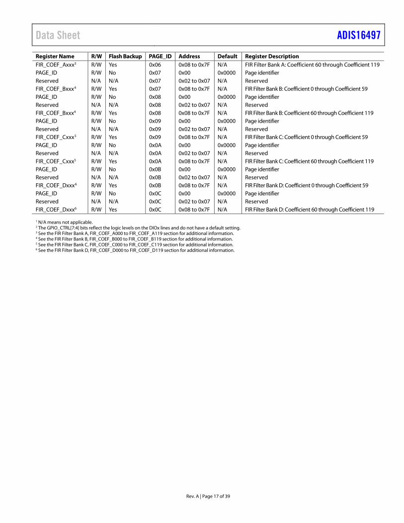
Register Name R/W Flash Backup PAGE_ID Address Default Register Description FIR_COEF_Axxx3 R/W Yes 0x06 0x08 to 0x7F N/A FIR Filter Bank A: Coefficient 60 through Coefficient 119 PAGE_ID R/W No 0x07 0x00 0x0000 Page identifier Reserved N/A N/A 0x07 0x02 to 0x07 N/A Reserved FIR_COEF_Bxxx4 R/W Yes 0x07 0x08 to 0x7F N/A FIR Filter Bank B: Coefficient 0 through Coefficient 59 PAGE_ID R/W No 0x08 0x00 0x0000 Page identifier Reserved N/A N/A 0x08 0x02 to 0x07 N/A Reserved FIR_COEF_Bxxx4 R/W Yes 0x08 0x08 to 0x7F N/A FIR Filter Bank B: Coefficient 60 through Coefficient 119 PAGE_ID R/W No 0x09 0x00 0x0000 Page identifier Reserved N/A N/A 0x09 0x02 to 0x07 N/A Reserved FIR_COEF_Cxxx5 R/W Yes 0x09 0x08 to 0x7F N/A FIR Filter Bank C: Coefficient 0 through Coefficient 59 PAGE_ID R/W No 0x0A 0x00 0x0000 Page identifier Reserved N/A N/A 0x0A 0x02 to 0x07 N/A Reserved FIR_COEF_Cxxx5 R/W Yes 0x0A 0x08 to 0x7F N/A FIR Filter Bank C: Coefficient 60 through Coefficient 119 PAGE_ID R/W No 0x0B 0x00 0x0000 Page identifier Reserved N/A N/A 0x0B 0x02 to 0x07 N/A Reserved FIR_COEF_Dxxx6 R/W Yes 0x0B 0x08 to 0x7F N/A FIR Filter Bank D: Coefficient 0 through Coefficient 59 PAGE_ID R/W No 0x0C 0x00 0x0000 Page identifier Reserved N/A N/A 0x0C 0x02 to 0x07 N/A Reserved FIR_COEF_Dxxx6 R/W Yes 0x0C 0x08 to 0x7F N/A FIR Filter Bank D: Coefficient 60 through Coefficient 119
1 N/A means not applicable. 2 The GPIO_CTRL[7:4] bits reflect the logic levels on the DIOx lines and do not have a default setting. 3 See the FIR Filter Bank A, FIR_COEF_A000 to FIR_COEF_A119 section for additional information. 4 See the FIR Filter Bank B, FIR_COEF_B000 to FIR_COEF_B119 section for additional information. 5 See the FIR Filter Bank C, FIR_COEF_C000 to FIR_COEF_C119 section for additional information. 6 See the FIR Filter Bank D, FIR_COEF_D000 to FIR_COEF_D119 section for additional information.
ADIS16497 Data Sheet
Rev. A | Page 18 of 39
USER REGISTER DEFINTIONS PAGE NUMBER (PAGE_ID) The contents in the PAGE_ID register (see Table 13 and Table 14) contain the current page setting, and provide a control for selecting another page for SPI access. For example, set DIN = 0x8002 to select Page 2 for SPI-based user access. See Table 12 for the page assignments associated with each user accessible register.
Table 13. PAGE_ID Register Definition Page Addresses Default Access Flash Backup 0x00 0x00, 0x01 0x0000 R/W No
Table 14. PAGE_ID Bit Descriptions Bits Description [15:0] Page number, binary numerical format
DATA/SAMPLE COUNTER (DATA_CNT) The DATA_CNT register (see Table 15 and Table 16) is a continu-ous, real-time, sample counter. It starts at 0x0000, increments every time the output data registers update, and wraps around from 0xFFFF (65,535 decimal) to 0x0000 (0 decimal).
Table 15. DATA_CNT Register Definition Page Addresses Default Access Flash Backup 0x00 0x04, 0x05 Not applicable R No
Table 16. DATA_CNT Bit Descriptions Bits Description [15:0] Data counter, binary format
STATUS/ERROR FLAG INDICATORS (SYS_E_FLAG) The SYS_E_FLAG register (see Table 17 and Table 18) provides various error flags. Reading this register causes all of its bits to return to 0, with the exception of Bit 7. If an error condition persists, its flag (bit) automatically returns to an alarm value of 1.
Table 17. SYS_E_FLAG Register Definition Page Addresses Default Access Flash Backup 0x00 0x08, 0x09 0x0000 R No
Table 18. SYS_E_FLAG Bit Descriptions Bits Description 15 Watchdog timer flag. A 1 indicates the ADIS16497
automatically resets itself to clear an issue. [14:9] Not used. 8 Sync error. A 1 indicates the sample timing is not scaling
correctly, when operating in PPS mode (FNCTIO_CTRL, Bit 8 = 1, see Table 144). When this error occurs, verify that the input sync frequency is correct and that SYNC_SCALE (see Table 154) has the correct value.
7 Processing overrun. A 1 indicates the occurrence of a processing overrun. Initiate a reset to recover. Replace the ADIS16497 if this error persists.
6 Flash memory update failure. A 1 indicates that the most recent flash memory update failed (GLOB_CMD, Bit 3, see Table 142). Repeat the test and replace the ADIS16497 if this error persists.
5 Sensor failure. A 1 indicates failure in at least one of the inertial sensors. Read the DIAG_STS register (see Table 20) to determine which sensor is failing. Replace the ADIS16497 if the error persists, when it is operating in static inertial conditions.
4 Not used. 3 SPI communication error. A 1 indicates that the total
number of SCLK cycles is not equal to an integer multiple of 16. Repeat the previous communication sequence to recover. Persistence in this error can indicate a weakness in the SPI service from the master processor.
2 SRAM error condition. A 1 indicates a failure in the CRC (period = 20 ms) between the SRAM and flash memory. Initiate a reset to recover. Replace the ADIS16497 if this error persists.
1 Boot memory failure. A 1 indicates that the device booted up using code from the backup memory bank. Replace the ADIS16497 if this error occurs.
0 Not used.

Data Sheet ADIS16497
Rev. A | Page 19 of 39
SELF TEST ERROR FLAGS (DIAG_STS) SYS_E_FLAG, Bit 5 (see Table 18) contains the pass/fail result (0 = pass) for the on demand self test (ODST) operations, whereas the DIAG_STS register (see Table 19 and Table 20) contains pass/fail flags (0 = pass) for each inertial sensor. Reading the DIAG_STS register causes all of its bits to restore to 0. The bits in DIAG_STS return to 1 if the error conditions persists.
Table 19. DIAG_STS Register Definition Page Addresses Default Access Flash Backup 0x00 0x0A, 0x0B 0x0000 R No
Table 20. DIAG_STS Bit Descriptions Bits Description (Default = 0x0000) [15:6] Not used 5 Self test failure, z-axis accelerometer (1 means failure) 4 Self test failure, y-axis accelerometer (1 means failure) 3 Self test failure, x-axis accelerometer (1 means failure) 2 Self test failure, z-axis gyroscope (1 means failure) 1 Self test failure, y-axis gyroscope (1 means failure) 0 Self test failure, x-axis gyroscope (1 means failure)
INTERNAL TEMPERATURE (TEMP_OUT) The TEMP_OUT register (see Table 21 and Table 22) provides a coarse measurement of the temperature inside of the ADIS16497. This data is useful for monitoring relative changes in the thermal environment. Table 23 provides several examples of the data format for the TEMP_OUT register.
Table 21. TEMP_OUT Register Definition Page Addresses Default Access Flash Backup 0x00 0x0E, 0x0F Not applicable R No
Table 22. TEMP_OUT Bit Definitions Bits Description [15:0] Temperature data; twos complement, 1°C per 80 LSB,
25°C = 0x0000
Table 23. TEMP_OUT Data Format Examples Temperature (°C) Decimal Hex Binary +85 +4800 0x12C0 0001 0010 1100 0000 +25 + 2/80 +2 0x0002 0000 0000 0000 0010 +25 + 1/80 +1 0x0001 0000 0000 0000 0001 +25 0 0x0000 0000 0000 0000 0000 +25 – 1/80 −1 0xFFFF 1111 1111 1111 1111 +25 – 2/80 −2 0xFFFE 1111 1111 1111 1110 −40 −5200 0xEBB0 1110 1011 1011 0000
GYROSCOPE DATA The gyroscopes in the ADIS16497 measure the angular rate of rotation around three orthogonal axes (x, y, and z). Figure 30 shows the orientation of each gyroscope axis, which defines the direction of rotation that produces a positive response in each of the angular rate measurements.
Each gyroscope has two output data registers. Figure 29 shows how these two registers combine to support a 32-bit, twos complement data format for the x-axis gyroscope measurements. This format also applies to the y-axis and z-axis as well.
X-AXIS GYROSCOPE DATA
0 1515 0
X_GYRO_OUT X_GYRO_LOW
1506
1-02
9
Figure 29. Gyroscope Output Data Structure
Gyroscope Measurement Range/Scale Factor
Table 24 provides the range and scale factor (KG) for the angular rate (gyroscope) measurements in each ADIS16497 model.
Table 24. Gyroscope Measurement Range and Scale Factors Model Range Scale Factor, KG ADIS16497-1BMLZ ±125°/sec 0.00625°/sec/LSB ADIS16497-2BMLZ ±450°/sec 0.025°/sec/LSB ADIS16497-3BMLZ ±2000°/sec 0.1°/sec/LSB
Gyroscope Data Formatting
Table 25 and Table 26 offer various numerical examples that demonstrate the format of the rotation rate data in both 16-bit and 32-bit formats. See Table 24 for the scale factor (KG) associated with each ADIS16497 model.
Table 25. 16-Bit Gyroscope Data Format Examples Rotation Rate (°/sec) Decimal Hex Binary+10000 KG +10,000 0x2710 0010 0111 0001 0000 +2 KG +2 0x0002 0000 0000 0000 0010 +KG +1 0x0001 0000 0000 0000 0001 0°/sec 0 0x0000 0000 0000 0000 0000 −KG −1 0xFFFF 1111 1111 1111 1111 −2 KG −2 0xFFFE 1111 1111 1111 1110 −10000 KG −10,000 0xD8F0 1101 1000 1111 0000
Table 26. 32-Bit Gyroscope Data Format Examples Rotation Rate (°/sec) Decimal Hexadecimal +10000 KG +655,360,000 0x27100000+KG/215 +2 0x00000002+KG/216 +1 0x000000010 0 0x0000000−KG /216 −1 0xFFFFFFFF−KG /215 −2 0xFFFFFFFE−10000 KG −655,360,000 0xD8F00000

ADIS16497 Data Sheet
Rev. A | Page 20 of 39
PIN 1PIN 23
ωY
Y-AXIS
ωX
X-AXIS
Z-AXIS
ωZ
1506
1-03
0
Figure 30. Gyroscope Axis and Polarity Assignments
X-Axis Gyroscope (X_GYRO_LOW, X_GRYO_OUT)
The X_GYRO_LOW (see Table 27 and Table 28) and X_GRYO_ OUT (see Table 29 and Table 30) registers contain the gyroscope data for the x-axis.
Table 27. X_GYRO_LOW Register Definition Page Addresses Default Access Flash Backup 0x00 0x10, 0x11 Not applicable R No
Table 28. X_GYRO_LOW Bit Descriptions Bits Description [15:0] X-axis gyroscope data; low word
Table 29. X_GYRO_OUT Register Definition Page Addresses Default Access Flash Backup 0x00 0x12, 0x13 Not applicable R No
Table 30. X_GYRO_OUT Bit Descriptions Bits Description [15:0] X-axis gyroscope data; high word; twos complement,
0°/sec = 0x0000, see Table 24 for scale factor
Y-Axis Gyroscope (Y_GYRO_LOW, Y_GYRO_OUT)
The Y_GYRO_LOW (see Table 31 and Table 32) and Y_GRYO_ OUT (see Table 33 and Table 34) registers contain the gyroscope data for the y-axis.
Table 31. Y_GYRO_LOW Register Definition Page Addresses Default Access Flash Backup 0x00 0x14, 0x15 Not applicable R No
Table 32. Y_GYRO_LOW Bit Descriptions Bits Description [15:0] Y-axis gyroscope data; low word
Table 33. Y_GYRO_OUT Register Definition Page Addresses Default Access Flash Backup 0x00 0x16, 0x17 Not applicable R No
Table 34. Y_GYRO_OUT Bit Descriptions Bits Description [15:0] Y-axis gyroscope data; high word; twos complement,
0°/sec = 0x0000, see Table 24 for scale factor
Z-Axis Gyroscope (Z_GYRO_LOW, Z_GYRO_OUT)
The Z_GYRO_LOW (see Table 35 and Table 36) and Z_GRYO_ OUT (see Table 37 and Table 38) registers contain the gyroscope data for the z-axis.
Table 35. Z_GYRO_LOW Register Definition Page Addresses Default Access Flash Backup 0x00 0x18, 0x19 Not applicable R No
Table 36. Z_GYRO_LOW Bit Descriptions Bits Description [15:0] Z-axis gyroscope data; additional resolution bits
Table 37. Z_GYRO_OUT Register Definition Page Addresses Default Access Flash Backup 0x00 0x1A, 0x1B Not applicable R No
Table 38. Z_GYRO_OUT Bit Descriptions Bits Description [15:0] Z-axis gyroscope data; high word; twos complement,
0°/sec = 0x0000, see Table 24 for scale factor
Data Sheet ADIS16497
Rev. A | Page 21 of 39
PIN 1PIN 23
aY
Y-AXIS
X-AXIS
aX
Z-AXIS
aZ
1506
1-03
1
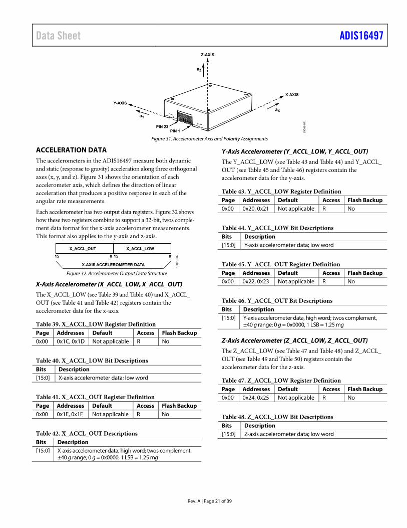
Figure 31. Accelerometer Axis and Polarity Assignments
ACCELERATION DATA The accelerometers in the ADIS16497 measure both dynamic and static (response to gravity) acceleration along three orthogonal axes (x, y, and z). Figure 31 shows the orientation of each accelerometer axis, which defines the direction of linear acceleration that produces a positive response in each of the angular rate measurements.
Each accelerometer has two output data registers. Figure 32 shows how these two registers combine to support a 32-bit, twos comple-ment data format for the x-axis accelerometer measurements. This format also applies to the y-axis and z-axis.
X-AXIS ACCELEROMETER DATA
0 1515 0
X_ACCL_OUT X_ACCL_LOW
1506
1-03
2
Figure 32. Accelerometer Output Data Structure
X-Axis Accelerometer (X_ACCL_LOW, X_ACCL_OUT)
The X_ACCL_LOW (see Table 39 and Table 40) and X_ACCL_ OUT (see Table 41 and Table 42) registers contain the accelerometer data for the x-axis.
Table 39. X_ACCL_LOW Register Definition Page Addresses Default Access Flash Backup 0x00 0x1C, 0x1D Not applicable R No
Table 40. X_ACCL_LOW Bit Descriptions Bits Description [15:0] X-axis accelerometer data; low word
Table 41. X_ACCL_OUT Register Definition Page Addresses Default Access Flash Backup 0x00 0x1E, 0x1F Not applicable R No
Table 42. X_ACCL_OUT Descriptions Bits Description [15:0] X-axis accelerometer data, high word; twos complement,
±40 g range; 0 g = 0x0000, 1 LSB = 1.25 mg
Y-Axis Accelerometer (Y_ACCL_LOW, Y_ACCL_OUT)
The Y_ACCL_LOW (see Table 43 and Table 44) and Y_ACCL_ OUT (see Table 45 and Table 46) registers contain the accelerometer data for the y-axis.
Table 43. Y_ACCL_LOW Register Definition Page Addresses Default Access Flash Backup 0x00 0x20, 0x21 Not applicable R No
Table 44. Y_ACCL_LOW Bit Descriptions Bits Description [15:0] Y-axis accelerometer data; low word
Table 45. Y_ACCL_OUT Register Definition Page Addresses Default Access Flash Backup 0x00 0x22, 0x23 Not applicable R No
Table 46. Y_ACCL_OUT Bit Descriptions Bits Description [15:0] Y-axis accelerometer data, high word; twos complement,
±40 g range; 0 g = 0x0000, 1 LSB = 1.25 mg
Z-Axis Accelerometer (Z_ACCL_LOW, Z_ACCL_OUT)
The Z_ACCL_LOW (see Table 47 and Table 48) and Z_ACCL_ OUT (see Table 49 and Table 50) registers contain the accelerometer data for the z-axis.
Table 47. Z_ACCL_LOW Register Definition Page Addresses Default Access Flash Backup 0x00 0x24, 0x25 Not applicable R No
Table 48. Z_ACCL_LOW Bit Descriptions Bits Description [15:0] Z-axis accelerometer data; low word
ADIS16497 Data Sheet
Rev. A | Page 22 of 39
Table 49. Z_ACCL_OUT Register Definition Page Addresses Default Access Flash Backup 0x00 0x26, 0x27 Not applicable R No
Table 50. Z_ACCL_OUT Bit Descriptions Bits Description [15:0] Z-axis accelerometer data, high word; twos complement,
±40 g range; 0 g = 0x0000, 1 LSB = 1.25 mg
Accelerometer Resolution
Table 51 and Table 52 offer various numerical examples that demonstrate the format of the linear acceleration data in both 16-bit and 32-bit formats.
Table 51. 16-Bit Accelerometer Data Format Examples Acceleration Decimal Hex Binary +40 g +32,000 0x7D00 0111 1101 0000 0000 +2.5 mg +2 0x0002 0000 0000 0000 0010 +1.25 mg +1 0x0001 0000 0000 0000 0001 0 mg 0 0x0000 0000 0000 0000 0000 −1.25 mg −1 0xFFFF 1111 1111 1111 1111 −2.5 mg −2 0xFFFE 1111 1111 1111 1110 −40 g −32,000 0x8300 1000 0011 0000 0000
Table 52. 32-Bit Accelerometer Data Format Examples Acceleration Decimal Hexadecimal +40 g +2,097,152,000 0x7D000000 +1.25/215 mg +2 0x00000002 +1.25/216 mg +1 0x00000001 0 mg 0 0x00000000 −1.25/216 mg −1 0xFFFFFFFF −1.25/215 mg −2 0xFFFFFFFE −40 g −2,097,152,000 0x83000000
TIME STAMP When using PPS mode (FNCTIO_CTRL, Bits[8:7] = 11 (binary), see Table 144), the TIME_STAMP register (see Table 53 and Table 54) provides the time between the most recent pulse on the input clock signal and the most recent data update.
Table 53. TIME_STAMP Register Definition Page Addresses Default Access Flash Backup 0x00 0x28, 0x29 Not applicable R No
Table 54. TIME_STAMP Bit Descriptions Bits Description [15:0] Time stamp, binary format.
1 LSB = 1/fSM (see Figure 14, Figure 15, and Table 154). The leading edge of the input clock pulse resets the value in this register to 0x0000.
When using the decimation filter (DEC_RATE > 0x0000) the value in the TIME_STAMP register represents the time of the first sample (taken at the rate of fSM, per Figure 14 and Figure 15). For example, when DEC_RATE = 0x0003, the decimation filter reduces the update by a factor of four and the TIME_STAMP register updates to 1 (decimal) during the first data update, then to 5 on the second update, 9 on the third update, for example; until the next clock signal pulse.
CYCLICAL REDUNDANDCY CHECK (CRC-32) The ADIS16497 performs a CRC-32 computation, using the data registers that are shown in Table 55.
Table 55. CRC-32 Source Data and Example Values Register Example Value SYS_E_FLAG 0x0000 TEMP_OUT 0x083A X_GYRO_LOW 0x0000 X_GYRO_OUT 0xFFF7 Y_GYRO_LOW 0x0000 Y_GYRO_OUT 0xFFFE Z_GYRO_LOW 0x0000 Z_GYRO_OUT 0x0001 X_ACCL_LOW 0x5001 X_ACCL_OUT 0x0003 Y_ACCL_LOW 0xE00A Y_ACCL_OUT 0x0015 Z_ACCL_LOW 0xC009 Z_ACCL_OUT 0x0320 TIME_STAMP 0x8A54
The CRC_LWR (see Table 56 and Table 57) and CRC_UPR (see Table 58 and Table 59) registers contain the result of the CRC-32 computation. For the example, the register values from Table 55 are,
CRC_LWR = 0x15B4
CRC_UPR = 0xB6C8
Table 56. CRC_LWR Register Definition Page Addresses Default Access Flash Backup 0x00 0x2A, 0x2B Not applicable R No
Table 57. CRC_LWR Bit Descriptions Bits Description [15:0] CRC-32 code from most recent BRF, lower word
Table 58. CRC_UPR Register Definition Page Addresses Default Access Flash Backup 0x00 0x2C, 0x2D Not applicable R No
Table 59. CRC_UPR Bit Descriptions Bits Description [15:0] CRC-32 code from most recent BRF, upper word

Data Sheet ADIS16497
Rev. A | Page 23 of 39
PIN 1PIN 23
∆θY
Y-AXIS
∆θX
X-AXIS
Z-AXIS
∆θZ
1506
1-03
4
Figure 33. Delta Angle Axis and Polarity Assignments
DELTA ANGLES In addition to the angular rate of rotation (gyroscope) measure-ments around each axis (x, y, and z), the ADIS16497 also provides delta angle measurements that represent a computation of angular displacement between each sample update. Figure 33 shows the orientation of each delta angle output, which defines the direction of rotation that produces a positive response in each of the angular displacement (delta angle) measurements.
The delta angle outputs represent an integration of the gyro-scope measurements and use the following formula for all three axes (x-axis displayed):
1
01,,, 2
1 D
ddDnxdDnx
SDnx f
where: ΔΘX is the delta angle measurement for the x-axis D is the decimation rate = DEC_RATE + 1 (see Table 150). fS is the sample rate. d is the incremental variable in the summation formula. ωx is the x-axis rate of rotation (gyroscope). n is the sample time, prior to the decimation filter.
When using the internal sample clock, fS is equal to 4250 SPS. When using the external clock option, fS is equal to the frequency of the external clock. The range in the delta angle registers accommodates the maximum rate of rotation (100°/sec), the nominal sample rate (4250 SPS), and an update rate of 1 Hz (DEC_RATE = 0x1099; divide by 4249 plus 1, see Table 150), all at the same time. When using an external clock that is higher than 4250 SPS, reduce the DEC_RATE setting to avoid over-ranging the delta angle registers.
Each axis of the delta angle measurements has two output data registers. Figure 34 shows how these two registers combine to support a 32-bit, twos complement data format for the x-axis delta angle measurements. This format also applies to the y-axis and z-axis.
X-AXIS DELTA ANGLE DATA
0 1515 0
X_DELTANG_OUT X_DELTANG_LOW
1506
1-03
3
Figure 34. Delta Angle Output Data Structure
Delta Angle Measurement Range
Table 60 offers the measurement range and scale factor for each ADIS16470 model.
Table 60. Delta Angle Measurement Range and Scale Factor Model Measurement Range, ±ΔΘMAX ADIS16497-1AMLZ ±360° ADIS16497-2AMLZ ±720° ADIS16497-3AMLZ ±2160°
X-Axis Delta Angle (X_DELTANG_LOW, X_DELTANG_OUT)
The X_DELTANG_LOW (see Table 61 and Table 62) and X_DELTANG_OUT (see Table 63 and Table 64) registers contain the delta angle data for the x-axis.
Table 61. X_DELTANG_LOW Register Definitions Page Addresses Default Access Flash Backup 0x00 0x40, 0x41 Not applicable R No
Table 62. X_DELTANG_LOW Bit Descriptions Bits Description [15:0] X-axis delta angle data; low word
Table 63. X_DELTANG_OUT Register Definitions Page Addresses Default Access Flash Backup 0x00 0x42, 0x43 Not applicable R No
Table 64. X_DELTANG_OUT Bit Descriptions Bits Description [15:0] X-axis delta angle data; twos complement, 0° = 0x0000,
1 LSB = ΔΘMAX/215 (see Table 60 for ΔΘMAX)
Y-Axis Delta Angle (Y_DELTANG_LOW, Y_DELTANG_OUT)
The Y_DELTANG_LOW (see Table 65 and Table 66) and Y_DELTANG_OUT (see Table 67 and Table 68) registers contain the delta angle data for the y-axis.
Table 65. Y_DELTANG_LOW Register Definitions Page Addresses Default Access Flash Backup 0x00 0x44, 0x45 Not applicable R No
ADIS16497 Data Sheet
Rev. A | Page 24 of 39
Table 66. Y_DELTANG_LOW Bit Descriptions Bits Description [15:0] Y-axis delta angle data; low word
Table 67. Y_DELTANG_OUT Register Definitions Page Addresses Default Access Flash Backup 0x00 0x46, 0x47 Not applicable R No
Table 68. Y_DELTANG_OUT Bit Descriptions Bits Description [15:0] Y-axis delta angle data; twos complement, 0° = 0x0000,
1 LSB = ΔΘMAX/215 (see Table 60 for ΔΘMAX)
Z-Axis Delta Angle (Z_DELTANG_LOW, Z_DELTANG_OUT)
The Z_DELTANG_LOW (see Table 69 and Table 70) and Z_DELTANG_OUT (see Table 71 and Table 72) registers contain the delta angle data for the z-axis.
Table 69. Z_DELTANG_LOW Register Definitions Page Addresses Default Access Flash Backup 0x00 0x48, 0x49 Not applicable R No
Table 70. Z_DELTANG_LOW Bit Descriptions Bits Description [15:0] Z-axis delta angle data; low word
Table 71. Z_DELTANG_OUT Register Definitions Page Addresses Default Access Flash Backup 0x00 0x4A, 0x4B Not applicable R No
Table 72. Z_DELTANG_OUT Bit Descriptions Bits Description [15:0] Z-axis delta angle data; twos complement, 0° = 0x0000,
1 LSB = ΔΘMAX/215 (see Table 60 for ΔΘMAX)
Delta Angle Resolution
Table 73 and Table 74 show various numerical examples that demonstrate the format of the delta angle data in both 16-bit and 32-bit formats.
Table 73. 16-Bit Delta Angle Data Format Examples Delta Angle (°) Decimal Hex Binary ΔΘMAX × (215−1)/215 +32,767 0x7FFF 0111 1111 1110 1111 +ΔΘMAX/214 +2 0x0002 0000 0000 0000 0010 +ΔΘMAX/215 +1 0x0001 0000 0000 0000 0001 0 0 0x0000 0000 0000 0000 0000 −ΔΘMAX/215 −1 0xFFFF 1111 1111 1111 1111 −ΔΘMAX/214 −2 0xFFFE 1111 1111 1111 1110 −ΔΘMAX −32,768 0x8000 1000 0000 0000 0000
Table 74. 32-Bit Delta Angle Data Format Examples Delta Angle (°) Decimal Hexadecimal +ΔΘMAX × (231 − 1)/231 +2,147,483,647 0x7FFFFFFF +ΔΘMAX/230 +2 0x00000002 +ΔΘMAX2000/231 +1 0x00000001 0 0 0x00000000 −ΔΘMAX/231 −1 0xFFFFFFFF −ΔΘMAX/230 −2 0xFFFFFFFE −ΔΘMAX −2,147,483,648 0x80000000
DELTA VELOCITY In addition to the linear acceleration measurements along each axis (x, y, and z), the ADIS16497 also provides delta velocity measurements that represent a computation of linear velocity change between each sample update. Figure 36 shows the orientation of each delta-velocity measurement, which defines the direction of linear velocity increase that produces a positive response in each of the delta velocity rate measurements.
The delta velocity outputs represent an integration of the accelera-tion measurements and use the following formula for all three axes (x-axis displayed):
( )∑−
=−++ +×=∆
1
01,,, 2
1 D
ddDnxdDnx
SDnx aa
fV
where: ΔVX is the delta velocity measurement for the x-axis. D is the decimation rate = DEC_RATE + 1 (see Table 150). fS is the sample rate. d is the incremental variable in the summation formula. ax is the x-axis rate of rotation (gyroscope). n is the sample time, prior to the decimation filter.
When using the internal sample clock, fS is equal to 4250 SPS. When using the external clock option, fS is equal to the frequency of the external clock. The range in the delta velocity registers accommodates the maximum linear acceleration (8 g), the nominal sample rate (4250 SPS), and an update rate of 1 Hz (DEC_RATE = 0x1099; divide by 4249 plus 1, see Table 150), all at the same time. When using an external clock that is higher than 4250 SPS, reduce the DEC_RATE setting to avoid overranging the delta velocity registers.
Each axis of the delta velocity measurements has two output data registers. Figure 35 shows how these two registers combine to support 32-bit, twos complement data format for the delta velocity measurements along the x-axis. This format also applies to the y-axis and x-axis.
X-AXIS DELTA ANGLE DATA
0 1515 0
X_DELTVEL_OUT X_DELTVEL_LOW
1506
1-03
5
Figure 35. Delta Angle Output Data Structure
Data Sheet ADIS16497
Rev. A | Page 25 of 39
PIN 1PIN 23
ΔVY
Y-AXIS
X-AXIS
ΔVX
Z-AXIS
ΔVZ
1506
1-03
6
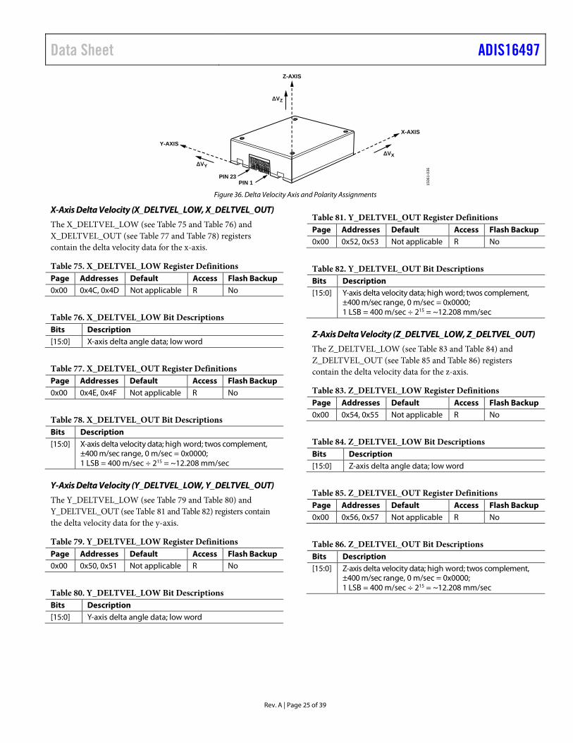
Figure 36. Delta Velocity Axis and Polarity Assignments
X-Axis Delta Velocity (X_DELTVEL_LOW, X_DELTVEL_OUT)
The X_DELTVEL_LOW (see Table 75 and Table 76) and X_DELTVEL_OUT (see Table 77 and Table 78) registers contain the delta velocity data for the x-axis.
Table 75. X_DELTVEL_LOW Register Definitions Page Addresses Default Access Flash Backup 0x00 0x4C, 0x4D Not applicable R No
Table 76. X_DELTVEL_LOW Bit Descriptions Bits Description [15:0] X-axis delta angle data; low word
Table 77. X_DELTVEL_OUT Register Definitions Page Addresses Default Access Flash Backup 0x00 0x4E, 0x4F Not applicable R No
Table 78. X_DELTVEL_OUT Bit Descriptions Bits Description [15:0] X-axis delta velocity data; high word; twos complement,
±400 m/sec range, 0 m/sec = 0x0000; 1 LSB = 400 m/sec ÷ 215 = ~12.208 mm/sec
Y-Axis Delta Velocity (Y_DELTVEL_LOW, Y_DELTVEL_OUT)
The Y_DELTVEL_LOW (see Table 79 and Table 80) and Y_DELTVEL_OUT (see Table 81 and Table 82) registers contain the delta velocity data for the y-axis.
Table 79. Y_DELTVEL_LOW Register Definitions Page Addresses Default Access Flash Backup 0x00 0x50, 0x51 Not applicable R No
Table 80. Y_DELTVEL_LOW Bit Descriptions Bits Description [15:0] Y-axis delta angle data; low word
Table 81. Y_DELTVEL_OUT Register Definitions Page Addresses Default Access Flash Backup 0x00 0x52, 0x53 Not applicable R No
Table 82. Y_DELTVEL_OUT Bit Descriptions Bits Description [15:0] Y-axis delta velocity data; high word; twos complement,
±400 m/sec range, 0 m/sec = 0x0000; 1 LSB = 400 m/sec ÷ 215 = ~12.208 mm/sec
Z-Axis Delta Velocity (Z_DELTVEL_LOW, Z_DELTVEL_OUT)
The Z_DELTVEL_LOW (see Table 83 and Table 84) and Z_DELTVEL_OUT (see Table 85 and Table 86) registers contain the delta velocity data for the z-axis.
Table 83. Z_DELTVEL_LOW Register Definitions Page Addresses Default Access Flash Backup 0x00 0x54, 0x55 Not applicable R No
Table 84. Z_DELTVEL_LOW Bit Descriptions Bits Description [15:0] Z-axis delta angle data; low word
Table 85. Z_DELTVEL_OUT Register Definitions Page Addresses Default Access Flash Backup 0x00 0x56, 0x57 Not applicable R No
Table 86. Z_DELTVEL_OUT Bit Descriptions Bits Description [15:0] Z-axis delta velocity data; high word; twos complement,
±400 m/sec range, 0 m/sec = 0x0000; 1 LSB = 400 m/sec ÷ 215 = ~12.208 mm/sec

ADIS16497 Data Sheet
Rev. A | Page 26 of 39
Delta Velocity Resolution
Table 87 and Table 88 show various numerical examples that demonstrate the format of the delta angle data in both 16-bit and 32-bit formats.
Table 87. 16-Bit Delta Velocity Data Format Examples Velocity (m/sec) Decimal Hex Binary +400 × (215 − 1)/215 +32,767 0x7FFF 0111 1111 1110 1111 +400/214 +2 0x0002 0000 0000 0000 0010 +400/215 +1 0x0001 0000 0000 0000 0001 0 0 0x0000 0000 0000 0000 0000 −400/215 −1 0xFFFF 1111 1111 1111 1111 −400/214 −2 0xFFFE 1111 1111 1111 1110 −400 −32,768 0x8000 1000 0000 0000 0000
Table 88. 32-Bit Delta Angle Data Format Examples Velocity (m/sec) Decimal Hex +400 × (231 − 1)/231 +2,147,483,647 0x7FFFFFFF+400/230 +2 0x00000002+400/231 +1 0x00000001 0 0 0x00000000 −400/231 −1 0xFFFFFFFF −400/230 −2 0xFFFFFFFE−400 −2,147,483,648 0x80000000
Burst Read Command, BURST_CMD
Reading the BURST_CMD register (see Table 89 and Table 90) starts the BRF. See Table 10, Table 11, Figure 5, and Figure 6 for more information on the BRF function.
Table 89. BURST_CMD Register Definitions Page Addresses Default Access Flash Backup 0x00 0x7C, 0x7D Not Applicable R No
Table 90. BURST_CMD Bit Descriptions Bits Description [15:0] Burst read command register
Product Identification, PROD_ID
The PROD_ID register (see Table 91 and Table 92) contains the numerical portion of the device number (16,497). See Figure 26 for an example of how to use a looping read of this register to validate the integrity of the communication.
Table 91. PROD_ID Register Definitions Page Addresses Default Access Flash Backup 0x00 0x7E, 0x7F 0x4071 R Yes
Table 92. PROD_ID Bit Descriptions Bits Description [15:0] Product identification = 0x4071
USER BIAS/SCALE ADJUSTMENT The signal chain of each inertial sensor (accelerometers, gyro-scopes) includes application of unique correction formulas that come from extensive characterization of bias, sensitivity, align-ment, and response to linear acceleration (gyroscopes) over a temperature range of −40°C to +85°C for the ADIS16497. These correction formulas are not accessible, but the user does have the opportunity to adjust the bias and the scale factor, for each sensor individually, through user accessible registers. These correction factors follow immediately after the factory derived correction formulas in the signal chain, which processes at a rate of 4250 Hz when using the internal sample clock (see fSM in Figure 14 and Figure 15).
Gyroscope Scale Adjustment, X_GYRO_SCALE
The X_GYRO_SCALE register (see Table 93 and Table 94) provides the user with the opportunity to adjust the scale factor for the x-axis gyroscopes. See Figure 37 for an illustration of how this scale factor influences the x-axis gyroscope data.
Table 93. X_GYRO_SCALE Register Definitions Page Addresses Default Access Flash Backup 0x02 0x04, 0x05 0x0000 R/W Yes
Table 94. X_GYRO_SCALE Bit Descriptions Bits Description [15:0] X-axis gyroscope scale correction; twos complement,
0x0000 = unity gain, 1 LSB = 1 ÷ 215 = ~0.003052%
X-AXISGYRO
FACTORYCALIBRATION
ANDFILTERING
X_GYRO_OUT X_GYRO_LOW
XG_BIAS_HIGH XG_BIAS_LOW
1 + X_GYRO_SCALE
1506
1-03
7
Figure 37. User Bias/Scale Adjustment Registers in Gyroscope Signal Path
Gyroscope Scale Adjustment, Y_GYRO_SCALE
The Y_GYRO_SCALE register (see Table 95 and Table 96) allows the user to adjust the scale factor for the y-axis gyroscopes. This register influences the y-axis gyroscope measurements in the same manner that X_GYRO_SCALE influences the x-axis gyroscope measurements (see Figure 37).
Table 95. Y_GYRO_SCALE Register Definitions Page Addresses Default Access Flash Backup 0x02 0x06, 0x07 0x0000 R/W Yes
Table 96. Y_GYRO_SCALE Bit Descriptions Bits Description [15:0] Y-axis gyroscope scale correction; twos complement,
0x0000 = unity gain, 1 LSB = 1 ÷ 215 = ~0.003052%
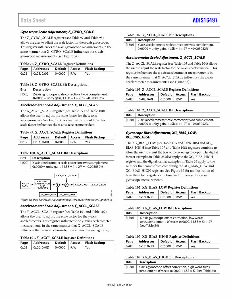
Data Sheet ADIS16497
Rev. A | Page 27 of 39
Gyroscope Scale Adjustment, Z_GYRO_SCALE
The Z_GYRO_SCALE register (see Table 97 and Table 98) allows the user to adjust the scale factor for the z-axis gyroscopes. This register influences the z-axis gyroscope measurements in the same manner that X_GYRO_SCALE influences the x-axis gyroscope measurements (see Figure 37).
Table 97. Z_GYRO_SCALE Register Definitions Page Addresses Default Access Flash Backup 0x02 0x08, 0x09 0x0000 R/W Yes
Table 98. Z_GYRO_SCALE Bit Descriptions Bits Description [15:0] Z-axis gyroscope scale correction; twos complement,
0x0000 = unity gain, 1 LSB = 1 ÷ 215 = ~0.003052%
Accelerometer Scale Adjustment, X_ACCL_SCALE
The X_ACCL_SCALE register (see Table 99 and Table 100) allows the user to adjust the scale factor for the x-axis accelerometers. See Figure 38 for an illustration of how this scale factor influences the x-axis accelerometer data.
Table 99. X_ACCL_SCALE Register Definitions Page Addresses Default Access Flash Backup 0x02 0x0A, 0x0B 0x0000 R/W Yes
Table 100. X_ACCL_SCALE Bit Descriptions Bits Description [15:0] X-axis accelerometer scale correction; twos complement,
0x0000 = unity gain, 1 LSB = 1 ÷ 215 = ~0.003052%
X-AXISACCL
FACTORYCALIBRATION
ANDFILTERING
X_ACCL_OUT X_ACCL_LOW
XA_BIAS_HIGH XA_BIAS_LOW
1 + X_ACCL_SCALE
1506
1-03
8
Figure 38. User Bias/Scale Adjustment Registers in Accelerometer Signal Path
Accelerometer Scale Adjustment, Y_ACCL_SCALE
The Y_ACCL_SCALE register (see Table 101 and Table 102) allows the user to adjust the scale factor for the y-axis accelerometers. This register influences the y-axis accelerometer measurements in the same manner that X_ACCL_SCALE influences the x-axis accelerometer measurements (see Figure 38).
Table 101. Y_ACCL_SCALE Register Definitions Page Addresses Default Access Flash Backup 0x02 0x0C, 0x0D 0x0000 R/W Yes
Table 102. Y_ACCL_SCALE Bit Descriptions Bits Description [15:0] Y-axis accelerometer scale correction; twos complement,
0x0000 = unity gain, 1 LSB = 1 ÷ 215 = ~0.003052%
Accelerometer Scale Adjustment, Z_ACCL_SCALE
The Z_ACCL_SCALE register (see Table 103 and Table 104) allows the user to adjust the scale factor for the z-axis accelerometers. This register influences the z-axis accelerometer measurements in the same manner that X_ACCL_SCALE influences the x-axis accelerometer measurements (see Figure 38).
Table 103. Z_ACCL_SCALE Register Definitions Page Addresses Default Access Flash Backup 0x02 0x0E, 0x0F 0x0000 R/W Yes
Table 104. Z_ACCL_SCALE Bit Descriptions Bits Description [15:0] Z-axis accelerometer scale correction; twos complement,
0x0000 = unity gain, 1 LSB = 1 ÷ 215 = ~0.003052%
Gyroscope Bias Adjustment, XG_BIAS_LOW, XG_BIAS_HIGH
The XG_BIAS_LOW (see Table 105 and Table 106) and XG_ BIAS_HIGH (see Table 107 and Table 108) registers combine to allow the user to adjust the bias of the x-axis gyroscopes. The digital format examples in Table 25 also apply to the XG_BIAS_HIGH register, and the digital format examples in Table 26 apply to the number that comes from combining the XG_BIAS_LOW and XG_BIAS_HIGH registers. See Figure 37 for an illustration of how these two registers combine and influence the x-axis gyroscope measurements.
Table 105. XG_BIAS_LOW Register Definitions Page Addresses Default Access Flash Backup 0x02 0x10, 0x11 0x0000 R/W Yes
Table 106. XG_BIAS_LOW Bit Descriptions Bits Description [15:0] X-axis gyroscope offset correction, low word;
twos complement, 0°/sec = 0x0000, 1 LSB = KG ÷ 216 (see Table 24)
Table 107. XG_BIAS_HIGH Register Definitions Page Addresses Default Access Flash Backup 0x02 0x12, 0x13 0x0000 R/W Yes
Table 108. XG_BIAS_HIGH Bit Descriptions Bits Description [15:0] X-axis gyroscope offset correction, high word twos
complement, 0°/sec = 0x0000, 1 LSB = KG (see Table 24)
ADIS16497 Data Sheet
Rev. A | Page 28 of 39
Gyroscope Bias Adjustment, YG_BIAS_LOW, YG_BIAS_HIGH
The YG_BIAS_LOW (see Table 109 and Table 110) and YG_ BIAS_HIGH (see Table 111 and Table 112) registers combine to allow the user to adjust the bias of the y-axis gyroscopes. The digital format examples in Table 25 also apply to the YG_BIAS_HIGH register, and the digital format examples in Table 26 apply to the number that comes from combining the YG_BIAS_LOW and YG_BIAS_HIGH registers. These registers influences the y-axis gyroscope measurements in the same manner that the XG_BIAS_ LOW and XG_BIAS_HIGH registers influence the x-axis gyroscope measurements (see Figure 37).
Table 109. YG_BIAS_LOW Register Definitions Page Addresses Default Access Flash Backup 0x02 0x14, 0x15 0x0000 R/W Yes
Table 110. YG_BIAS_LOW Bit Descriptions Bits Description [15:0] Y-axis gyroscope offset correction, low word; twos
complement, 0°/sec = 0x0000, 1 LSB = 0.005°/sec ÷ 216
Table 111. YG_BIAS_HIGH Register Definitions Page Addresses Default Access Flash Backup 0x02 0x16, 0x17 0x0000 R/W Yes
Table 112. YG_BIAS_HIGH Bit Descriptions Bits Description [15:0] Y-axis gyroscope offset correction, high word; twos
complement, 0°/sec = 0x0000, 1 LSB = 0.005°/sec
Gyroscope Bias Adjustment, ZG_BIAS_LOW, ZG_BIAS_HIGH
The ZG_BIAS_LOW (see Table 113 and Table 114) and ZG_ BIAS_HIGH (see Table 115 and Table 116) registers combine to allow the user to adjust the bias of the z-axis gyroscopes. The digital format examples in Table 25 also apply to the ZG_BIAS_HIGH register, and the digital format examples in Table 26 apply to the number that comes from combining the ZG_BIAS_LOW and ZG_BIAS_HIGH registers. These registers influence the z-axis gyroscope measurements in the same manner that the XG_BIAS_ LOW and XG_BIAS_HIGH registers influence the x-axis gyroscope measurements (see Figure 37).
Table 113. ZG_BIAS_LOW Register Definitions Page Addresses Default Access Flash Backup 0x02 0x18, 0x19 0x0000 R/W Yes
Table 114. ZG_BIAS_LOW Bit Descriptions Bits Description [15:0] Z-axis gyroscope offset correction, low word; twos
complement, 0°/sec = 0x0000, 1 LSB = 0.005°/sec ÷ 216
Table 115. ZG_BIAS_HIGH Register Definitions Page Addresses Default Access Flash Backup 0x02 0x1A, 0x1B 0x0000 R/W Yes
Table 116. ZG_BIAS_HIGH Bit Definitions Bits Description [15:0] Z-axis gyroscope offset correction, high word twos
complement, 0°/sec = 0x0000, 1 LSB = 0.005°/sec
Accelerometer Bias Adjustment, XA_BIAS_LOW, XA_BIAS_HIGH
The XA_BIAS_LOW (see Table 117 and Table 118) and XA_ BIAS_HIGH (see Table 119 and Table 120) registers combine to allow the user to adjust the bias of the x-axis accelerometers. The digital format examples in Table 51 also apply to the XA_BIAS_ HIGH register and the digital format examples in Table 52 apply to the number that comes from combining the XA_BIAS_LOW and XA_BIAS_HIGH registers. See Figure 38 for an illustration of how these two registers combine and influence the x-axis gyroscope measurements.
Table 117. XA_BIAS_LOW Register Definitions Page Addresses Default Access Flash Backup 0x02 0x1C, 0x1D 0x0000 R/W Yes
Table 118. XA_BIAS_LOW Bit Descriptions Bits Description [15:0] X-axis accelerometer offset correction, low word, twos
complement, 0 g = 0x0000, 1 LSB = 1.25 mg ÷ 216
Table 119. XA_BIAS_HIGH Register Definitions Page Addresses Default Access Flash Backup 0x02 0x1E, 0x1F 0x0000 R/W Yes
Table 120. XA_BIAS_HIGH Bit Descriptions Bits Description [15:0] X-axis accelerometer offset correction, high word,
twos complement, 0 g = 0x0000, 1 LSB = 1.25 mg
Accelerometer Bias Adjustment, YA_BIAS_LOW, YA_BIAS_HIGH
The YA_BIAS_LOW (see Table 121 and Table 122) and YA_ BIAS_HIGH (see Table 123 and Table 124) registers combine to allow the user to adjust the bias of the y-axis accelerometers. The digital format examples in Table 51 also apply to the YA_BIAS_ HIGH register, and the digital format examples in Table 52 apply to the number that comes from combining the YA_BIAS_LOW and YA_BIAS_HIGH registers. These registers influence the y-axis accelerometer measurements in the same manner that the XA_ BIAS_LOW and XA_BIAS_HIGH registers influence the x-axis accelerometer measurements (see Figure 38).
Data Sheet ADIS16497
Rev. A | Page 29 of 39
Table 121. YA_BIAS_LOW Register Definitions Page Addresses Default Access Flash Backup 0x02 0x20, 0x21 0x0000 R/W Yes
Table 122. YA_BIAS_LOW Bit Descriptions Bits Description [15:0] Y-axis accelerometer offset correction, low word, twos
complement, 0 g = 0x0000, 1 LSB = 1.25 mg ÷ 216
Table 123. YA_BIAS_HIGH Register Definitions Page Addresses Default Access Flash Backup 0x02 0x22, 0x23 0x0000 R/W Yes
Table 124. YA_BIAS_HIGH Bit Descriptions Bits Description [15:0] Y-axis accelerometer offset correction, high word,
twos complement, 0 g = 0x0000, 1 LSB = 1.25 mg
Accelerometer Bias Adjustment, ZA_BIAS_LOW, ZA_BIAS_HIGH
The ZA_BIAS_LOW (see Table 125 and Table 126) and ZA_ BIAS_HIGH (see Table 127 and Table 128) registers combine to allow the user to adjust the bias of the z-axis accelerometers. The digital format examples in Table 51 also apply to the ZA_BIAS_ HIGH register and the digital format examples in Table 52 apply to the number that comes from combining the ZA_BIAS_LOW and ZA_BIAS_HIGH registers. These registers influence the z-axis accelerometer measurements in the same manner that the XA_BIAS_LOW and XA_BIAS_HIGH registers influence the x-axis accelerometer measurements (see Figure 38).
Table 125. ZA_BIAS_LOW Register Definitions Page Addresses Default Access Flash Backup 0x02 0x24, 0x25 0x0000 R/W Yes
Table 126. ZA_BIAS_LOW Bit Descriptions Bits Description [15:0] Z-axis accelerometer offset correction, low word,
twos complement, 0 g = 0x0000, 1 LSB = 1.25 mg ÷ 216
Table 127. ZA_BIAS_HIGH Register Definitions Page Addresses Default Access Flash Backup 0x02 0x26, 0x27 0x0000 R/W Yes
Table 128. ZA_BIAS_HIGH Bit Descriptions Bits Description [15:0] Z-axis accelerometer offset correction, high word,
twos complement, 0 g = 0x0000, 1 LSB = 1.25 mg
SCRATCH REGISTERS, USER_SCR_X The USER_SCR_1 (see Table 129 and Table 130), USER_SCR_2 (see Table 131 and Table 132), USER_SCR_3 (see Table 133 and Table 134), and the USER_SCR_4 (see Table 135 and Table 136) registers provide four locations for the user to store information.
Table 129. USER_SCR_1 Register Definitions Page Addresses Default Access Flash Backup 0x02 0x74, 0x75 0x0000 R/W Yes
Table 130. USER_SCR_1 Bit Descriptions Bits Description [15:0] User defined
Table 131. USER_SCR_2 Register Definitions Page Addresses Default Access Flash Backup 0x02 0x76, 0x77 0x0000 R/W Yes
Table 132. USER_SCR_2 Bit Descriptions Bits Description [15:0] User defined
Table 133. USER_SCR_3 Register Definitions Page Addresses Default Access Flash Backup 0x02 0x78, 0x79 0x0000 R/W Yes
Table 134. USER_SCR_3 Bit Descriptions Bits Description [15:0] User defined
Table 135. USER_SCR_4 Register Definitions Page Addresses Default Access Flash Backup 0x02 0x7A, 0x7B 0x0000 R/W Yes
Table 136. USER_SCR_4 Bit Descriptions Bits Description [15:0] User defined
FLASH MEMORY ENDURANCE COUNTER, FLSHCNT_LOW, FLSHCNT_HIGH The FLSHCNT_LOW (see Table 137 and Table 138) and FLSHCNT_HIGH (see Table 139 and Table 140) registers combine to provide a 32-bit, binary counter that tracks the number of flash memory write cycles. In addition to the number of write cycles, the flash memory has a finite service lifetime, which depends on the junction temperature. Figure 39 provides guidance for estimating the retention life for the flash memory at specific junction temperatures. The junction temperature is approximately 7°C above the case temperature.
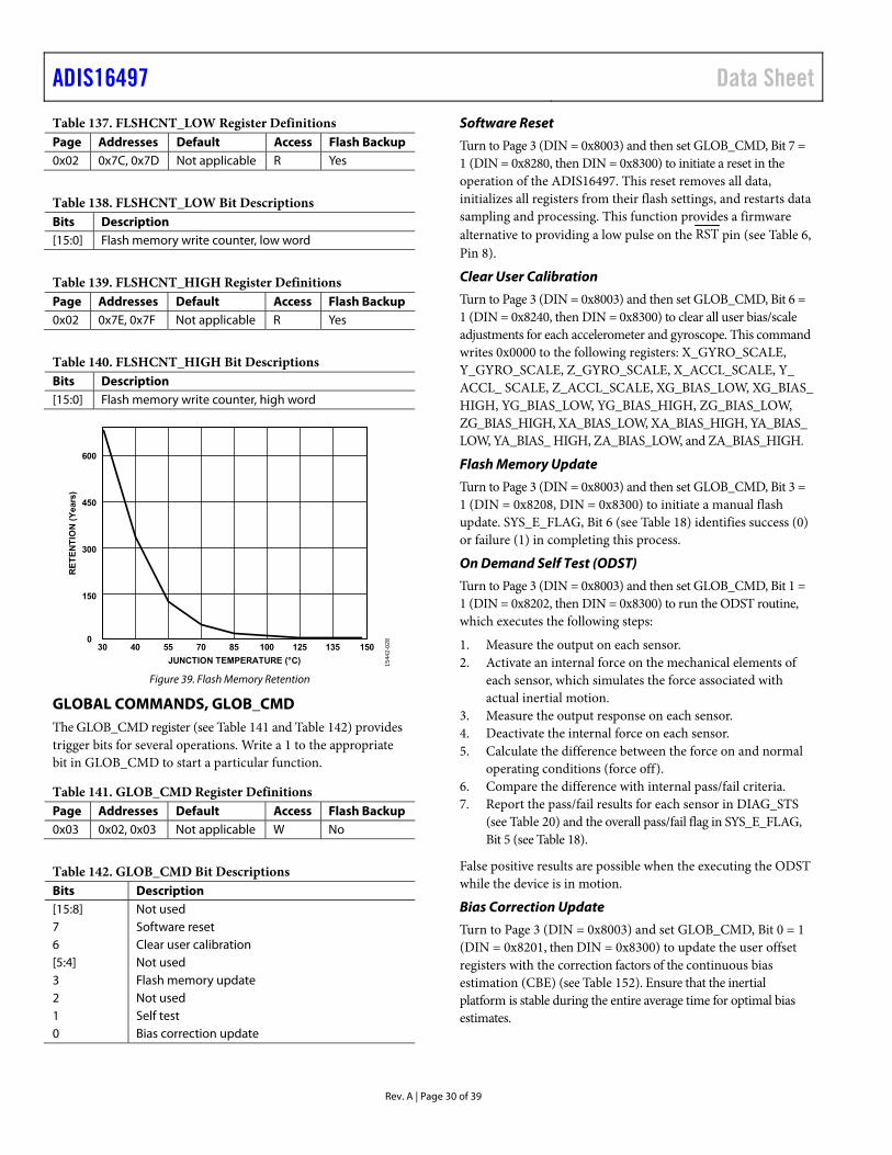
ADIS16497 Data Sheet
Rev. A | Page 30 of 39
Table 137. FLSHCNT_LOW Register Definitions Page Addresses Default Access Flash Backup 0x02 0x7C, 0x7D Not applicable R Yes
Table 138. FLSHCNT_LOW Bit Descriptions Bits Description [15:0] Flash memory write counter, low word
Table 139. FLSHCNT_HIGH Register Definitions Page Addresses Default Access Flash Backup 0x02 0x7E, 0x7F Not applicable R Yes
Table 140. FLSHCNT_HIGH Bit Descriptions Bits Description [15:0] Flash memory write counter, high word
600
450
300
150
030 40
RE
TE
NT
ION
(Y
ears
)
JUNCTION TEMPERATURE (°C)
55 70 85 100 125 135 150
1544
2-02
8
Figure 39. Flash Memory Retention
GLOBAL COMMANDS, GLOB_CMD The GLOB_CMD register (see Table 141 and Table 142) provides trigger bits for several operations. Write a 1 to the appropriate bit in GLOB_CMD to start a particular function.
Table 141. GLOB_CMD Register Definitions Page Addresses Default Access Flash Backup 0x03 0x02, 0x03 Not applicable W No
Table 142. GLOB_CMD Bit Descriptions Bits Description[15:8] Not used7 Software reset6 Clear user calibration [5:4] Not used3 Flash memory update 2 Not used1 Self test0 Bias correction update
Software Reset
Turn to Page 3 (DIN = 0x8003) and then set GLOB_CMD, Bit 7 = 1 (DIN = 0x8280, then DIN = 0x8300) to initiate a reset in the operation of the ADIS16497. This reset removes all data, initializes all registers from their flash settings, and restarts data sampling and processing. This function provides a firmware alternative to providing a low pulse on the RST pin (see Table 6, Pin 8).
Clear User Calibration
Turn to Page 3 (DIN = 0x8003) and then set GLOB_CMD, Bit 6 = 1 (DIN = 0x8240, then DIN = 0x8300) to clear all user bias/scale adjustments for each accelerometer and gyroscope. This command writes 0x0000 to the following registers: X_GYRO_SCALE, Y_GYRO_SCALE, Z_GYRO_SCALE, X_ACCL_SCALE, Y_ ACCL_ SCALE, Z_ACCL_SCALE, XG_BIAS_LOW, XG_BIAS_ HIGH, YG_BIAS_LOW, YG_BIAS_HIGH, ZG_BIAS_LOW, ZG_BIAS_HIGH, XA_BIAS_LOW, XA_BIAS_HIGH, YA_BIAS_ LOW, YA_BIAS_ HIGH, ZA_BIAS_LOW, and ZA_BIAS_HIGH.
Flash Memory Update
Turn to Page 3 (DIN = 0x8003) and then set GLOB_CMD, Bit 3 = 1 (DIN = 0x8208, DIN = 0x8300) to initiate a manual flash update. SYS_E_FLAG, Bit 6 (see Table 18) identifies success (0) or failure (1) in completing this process.
On Demand Self Test (ODST)
Turn to Page 3 (DIN = 0x8003) and then set GLOB_CMD, Bit 1 = 1 (DIN = 0x8202, then DIN = 0x8300) to run the ODST routine, which executes the following steps:
1. Measure the output on each sensor.2. Activate an internal force on the mechanical elements of
each sensor, which simulates the force associated withactual inertial motion.
3. Measure the output response on each sensor.4. Deactivate the internal force on each sensor.5. Calculate the difference between the force on and normal
operating conditions (force off).6. Compare the difference with internal pass/fail criteria.7. Report the pass/fail results for each sensor in DIAG_STS
(see Table 20) and the overall pass/fail flag in SYS_E_FLAG, Bit 5 (see Table 18).
False positive results are possible when the executing the ODST while the device is in motion.
Bias Correction Update
Turn to Page 3 (DIN = 0x8003) and set GLOB_CMD, Bit 0 = 1 (DIN = 0x8201, then DIN = 0x8300) to update the user offset registers with the correction factors of the continuous bias estimation (CBE) (see Table 152). Ensure that the inertial platform is stable during the entire average time for optimal bias estimates.
Data Sheet ADIS16497
Rev. A | Page 31 of 39
AUXILIARY I/O LINE CONFIGURATION, FNCTIO_CTRL The FNCTIO_CTRL register (see Table 143 and Table 144) provides configuration control for each I/O pin (DIO1, DIO2, DIO3, and DIO4). Each DIOx pin supports only one function at a time. When a single pin has two assignments, the enable bit for the lower priority function automatically resets to zero (disabling the lower priority function). The order of priority is as follows, from highest priority to lowest priority: data ready, sync clock input, and general-purpose. The ADIS16497 can take up to 20 ms to execute a write command to the FNCTIO_CTRL register. During this time, the operational state and the contents of the register remain unchanged, but the SPI interface supports normal communication (for accessing other registers).
Table 143. FNCTIO_CTRL Register Definitions Page Addresses Default Access Flash Backup 0x03 0x06, 0x07 0x000D R/W Yes
Table 144. FNCTIO_CTRL Bit Descriptions Bits Description [15:9] Not used 8 Sync clock mode
1 = PPS 0 = sync
7 Sync clock input enable 1 = enabled 0 = disabled
6 Sync clock input polarity 1 = rising edge 0 = falling edge
[5:4] Sync clock input line selection 00 = DIO1 01 = DIO2 10 = DIO3 11 = DIO4
3 Data ready enable: 1 = enabled 0 = disabled
2 Data ready polarity: 1 = positive 0 = negative
[1:0] Data ready line selection 00 = DIO1 01 = DIO2 10 = DIO3 11 = DIO4
Data Ready Indicator
The FNCTIO_CTRL, Bits[3:0] provide three configuration options for the data ready function: on/off, polarity, and DIOx line. The primary purpose this signal is to drive the interrupt control line of an embedded processor, which can synchronize data collection and minimize latency. The factory default assigns DIO2 as a positive polarity, data ready signal, which means the data in the output registers is valid when the DIO2 line is high (see Figure 21). This configuration works well when DIO2 drives an interrupt service pin that activates on a low to high pulse. Use the following sequence to change this assignment to DIO3 with negative polarity:
1. Turn to Page 3 (DIN = 0x8003).2. Set FNCTIO_CTRL, Bits[3:0] = 1000 (DIN = 0x860A, then
DIN = 0x8700).
The timing jitter on the data ready signal is typically within ±1.4 µs. When using DIO1 to support the data ready function, this signal can experience some premature pulses, which do not indicate the start of data production, during its start-up process.
If it is necessary to use DIO1 for this function, use it in conjunction with a delay or other control mechanism to prevent premature data acquisition activity during the start-up process.
Input Sync/Clock Control
The FNCTIO_CTRL, Bits[8:4] provide several configuration options for using one of the DIOx lines as an external clock signal and for controlling inertial sensor data collection and processing. For example, use the following sequence to establish DIO4 as a positive polarity, input clock pin that operates in sync mode and preserves the factory default setting for the data ready function:
1. Turn to Page 3 (DIN = 0x8003).2. Set FNCTIO_CTRL, Bits[7:0] = 0xFD (DIN = 0x86FD).3. Set FNCTIO_CTRL, Bits[15:8] = 0x00 (DIN = 0x8700).
In sync mode, the ADIS16497 disables its internal sample clock, and the frequency of the external clock signal establishes the rate of data collection and processing (fSM in Figure 14 and Figure 15). When using the PPS mode (FNCTIO_CTRL, Bit 8 = 1) the rate of data collection and production (fSM) is equal to the product of the external clock frequency and scale factor (KECSF) in the SYNC_SCALE register (see Table 154).

ADIS16497 Data Sheet
Rev. A | Page 32 of 39
GENERAL-PURPOSE I/O CONTROL, GPIO_CTRL When FNCTIO_CTRL does not configure a DIOx pin, the GPIO_CTRL register (see Table 145 and Table 146) provides user controls for general-purpose use of the DIOx pins. GPIO_CTRL, Bits[3:0], provide I/O assignment controls for each line. When the DIOx lines are inputs, monitor their level by reading GPIO_CTRL, Bits[7:4]. When the DIOx lines are used as outputs, set their level by writing to GPIO_CTRL, Bits[7:4].
For example, use the following sequence to set DIO1 and DIO3 as high and low output lines, respectively, and set DIO2 and DIO4 as input lines. Turn to Page 3 (DIN = 0x8003) and set GPIO_ CTRL, Bits[7:0] = 0x15 (DIN = 0x8815, then DIN = 0x8900).
Table 145. GPIO_CTRL Register Definitions1 Page Addresses Default Access Flash Backup 0x03 0x08, 0x09 0x00X0 R/W Yes
1 The GPIO_CTRL, Bits[7:4] reflect the logic levels on the DIOx lines and do not have a default setting.
Table 146. GPIO_CTRL Bit Descriptions 1 Bits Description [15:8] Don’t care 7 General-Purpose I/O Line 4 (DIO4) data level 6 General-Purpose I/O Line 3 (DIO3) data level 5 General-Purpose I/O Line 2 (DIO2) data level 4 General-Purpose I/O Line 1 (DIO1) data level 3 General-Purpose I/O Line 4 (DIO4) direction control
(1 = output, 0 = input) 2 General-Purpose I/O Line 3 (DIO3) direction control
(1 = output, 0 = input) 1 General-Purpose I/O Line 2 (DIO2) direction control
(1 = output, 0 = input) 0 General-Purpose I/O Line 1 (DIO1) direction control
(1 = output, 0 = input)
1 The GPIO_CTRL, Bits[7:4] reflect the logic levels on the DIOx lines and do not have a default setting.
MISCELLANEOUS CONFIGURATION, CONFIG The CONFIG register (see Table 147 and Table 148) provides configuration options for the linear g compensation in the gyroscopes (on/off) and the point of percussion alignment for the accelerometers (on/off).
Table 147. CONFIG Register Definitions Page Addresses Default Access Flash Backup 0x03 0x0A, 0x0B 0x00C0 R/W Yes
Table 148. CONFIG Bit Descriptions Bits Description [15:8] Not used 7 Linear g compensation for gyroscopes (1 = enabled) 6 Point of percussion alignment (1 = enabled) [5:0] Not used
Point of Percussion
CONFIG, Bit 6 offers a point of percussion alignment function that maps the accelerometer sensors to the corner of the package identified in Figure 40. To activate this feature, turn to Page 3 (DIN = 0x8003), then set CONFIG, Bit 6 = 1 (DIN = 0x8A40, then DIN = 0x8B00).
POINT OF PERCUSSIONALIGNMENT REFERENCE POINT.SEE CONFIG[6].
PIN 1PIN 23
1506
1-04
0
Figure 40. Point of Percussion Reference Point
LINEAR ACCELERATION ON EFFECT ON GYROSCOPE BIAS The ADIS16497 includes first-order compensation for the linear g effect in the gyroscopes, which uses the following model:
+
×
=
ωωω
AAA
LGLGLGLGLGLGLGLGLG
ωωω
ZPC
YPC
XPC
Z
Y
X
333231
232221
131211
ZC
YC
XC
The linear g correction factors, LGXY, apply correction for linear acceleration in all three directions to the data path of each gyro-scope (ωXPC, ωYPC, and ωZPC) at the rate of the data samples (4250 SPS when using the internal clock). CONFIG, Bit 7, provides an on/off control for this compensation. The factory default value for this bit activates this compensation.
To turn it off, turn to Page 3 (DIN = 0x8003) and set CONFIG, Bit 7 = 0 (DIN = 0x8A40, then DIN = 0x8B00). This command sequence also preserves the default setting for the point of percussion alignment function (on).
DECIMATION FILTER, DEC_RATE The DEC_RATE register (see Table 149 and Table 150) provides user control for the final filter stage (see Figure 17), which averages and decimates the accelerometers and gyroscopes data, and extends the time that the delta angle and delta velocity track between each update. The output sample rate is equal to 4250/(DEC_RATE + 1). For example, turn to Page 3 (DIN = 0x8003), and set DEC_RATE = 0x2A (DIN = 0x8C2A, then DIN = 0x8D00) to reduce the output sample rate to ~98.8 SPS (4250 ÷ 43).
Table 149. DEC_RATE Register Definitions Page Addresses Default Access Flash Backup 0x03 0x0C, 0x0D 0x0000 R/W Yes
Data Sheet ADIS16497
Rev. A | Page 33 of 39
Table 150. DEC_RATE Bit Descriptions Bits Description [15:11] Don’t care [10:0] Decimation rate, binary format, maximum = 4249
CONTINUOUS BIAS ESTIMATION (CBE), NULL_CNFG The NULL_CNFG register (see Table 151 and Table 152) provides the configuration controls for the CBE, which associates with the bias correction update command in GLOB_CMD, Bit 0 (see Table 142). NULL_CNFG, Bits[3:0], establishes the total average time (tA) for the bias estimates and NULL_CNFG, Bits[13:8], provide on/off controls for each sensor. The factory default configuration for NULL_CNFG enables the bias null command for the gyroscopes, disables the bias null command for the accelerometers, and sets the average time to ~26.64 sec.
When a sensor bit in NULL_CNFG is active (equal to 1), setting GLOB_CMD, Bit 0 = 1 (DIN sequence: 0x8003, 0x8201, 0x8300) causes its bias correction register to automatically update with a value that corrects for its present bias error (from the CBE). For example, setting NULL_CNFG, Bit 8 equal to 1 causes an update in the XG_BIAS_LOW (see Table 106) and XG_BIAS_HIGH (see Table 108) registers.
Table 151. NULL_CNFG Register Definitions Page Addresses Default Access Flash Backup 0x03 0x0E, 0x0F 0x070A R/W Yes
Table 152. NULL_CNFG Bit Descriptions Bits Description [15:14] Not used 13 Z-axis acceleration bias correction enable (1 = enabled) 12 Y-axis acceleration bias correction enable (1 = enabled) 11 X-axis acceleration bias correction enable (1 = enabled) 10 Z-axis gyroscope bias correction enable (1 = enabled) 9 Y-axis gyroscope bias correction enable (1 = enabled) 8 X-axis gyroscope bias correction enable (1 = enabled) [7:4] Not used [3:0] Time base control (TBC), range: 0 to 13 (default = 10);
tB = 2TBC/4250, time base; tA = 64 × tB, average time
SCALING THE INPUT CLOCK (PPS MODE), SYNC_SCALE The PPS mode (FNCTIO_CTRL, Bit 8 = 1, see Table 144) supports the use of an input sync frequency that is slower than the data sample rates of the inertial sensors. This mode supports a frequency range of 1 Hz to 128 Hz for the input sync mode. In this mode, the data sample rate is equal to the product of the value in the SYNC_SCALE register (see Table 153 and Table 154) and the input sync frequency. For example, the following command sequence sets the data collection and processing rate (fSM in Figure 14 and Figure 15) to 4000 Hz (SYNC_SCALE = 0x0FA0) when using a 1 Hz signal on the DIO3 line as the external clock input, and preserves the factory default configuration for the data ready signal:
1. Turn to Page 3 (DIN = 0x8003).2. Set SYNC_SCALE, Bits[7:0] = 0xA0 (DIN = 0x90A0).3. Set SYNC_SCALE, Bits[15:8] = 0x0F (DIN = 0x910F).4. Set FNCTIO_CTRL, Bits[7:0] = 0xFD (DIN = 0x86ED).Set FNCTIO_CTRL, Bits[15:8] = 0x00 (DIN = 0x8701).
Table 153. SYNC_SCALE Register Definitions Page Addresses Default Access Flash Backup 0x03 0x10, 0x11 0x109A R/W Yes
Table 154. SYNC_SCALE Bit Descriptions Bits Description [15:0] External clock scale factor (KECSF), binary format
Measurement Range Identifier, RANG_MDL
The RANG_MDL register (see Table 155 and Table 156) provides a convenient method for identifying the model (and gyroscope measurement range) of the ADIS16497.
Table 155. RANG_MDL Register Definitions1 Page Addresses Default Access Flash Backup 0x03 0x12, 0x13 N/A R N/A
1 N/A means not applicable.
Table 156. RANG_MDL Bit Descriptions Bits Description [15:3] Not used [3:0] 0011 = ADIS16497-1AMLZ (±125°/sec)
0111 = ADIS16497-2AMLZ (±450°/sec)
1111 = ADIS16497-3AMLZ (±2000°/sec)
ADIS16497 Data Sheet
Rev. A | Page 34 of 39
FIR FILTERS FIR Filters Control, FILTR_BNK_0, FILTR_BNK_1
The FILTR_BNK_0 (see Table 157 and Table 158) and FILTR_ BNK_1 (see Table 159 and Table 160) registers provide the configuration controls for the FIR filter bank in the signal chain of each sensor (see Figure 17). These registers provide on/off control for the FIR bank for each inertial sensor, along with the FIR bank (A, B, C, or D) that each sensor uses.
Table 157. FILTR_BNK_0 Register Definitions Page Addresses Default Access Flash Backup 0x03 0x16, 0x17 0x0000 R/W Yes
Table 158. FILTR_BNK_0 Bit Descriptions Bits Description (Default = 0x0000) 15 Don’t care 14 Y-axis accelerometer filter enable (1 = enabled) [13:12] Y-axis accelerometer filter bank selection 00 = Bank A 01 = Bank B 10 = Bank C 11 = Bank D 11 X-axis accelerometer filter enable (1 = enabled) [10:9] X-axis accelerometer filter bank selection 00 = Bank A 01 = Bank B 10 = Bank C 11 = Bank D 8 Z-axis gyroscope filter enable (1 = enabled) [7:6] Z-axis gyroscope filter bank selection 00 = Bank A 01 = Bank B 10 = Bank C 11 = Bank D 5 Y-axis gyroscope filter enable (1 = enabled) [4:3] Y-axis gyroscope filter bank selection 00 = Bank A 01 = Bank B 10 = Bank C 11 = Bank D 2 X-axis gyroscope filter enable (1 = enabled) [1:0] X-axis gyroscope filter bank selection 00 = Bank A 01 = Bank B 10 = Bank C 11 = Bank D
Table 159. FILTR_BNK_1 Register Definitions Page Addresses Default Access Flash Backup 0x03 0x18, 0x19 0x0000 R/W Yes
Table 160. FILTR_BNK_1 Bit Descriptions Bits Description [15:3] Don’t care 2 Z-axis accelerometer filter enable (1 = enabled) [1:0] Z-axis accelerometer filter bank selection: 00 = Bank A 01 = Bank B 10 = Bank C 11 = Bank D
FIR Filter Bank Memory Maps
The ADIS16497 provides four FIR filter banks to configure and select for each individual inertial sensor using the FILTR_BNK_0 (see Table 158) and FILTR_BNK_1 (see Table 160) registers. Each FIR filter bank (A, B, C, and D) has 120 taps that consume two pages of memory. The coefficient associated with each tap, in each filter bank, has its own dedicated register that uses a 16-bit, twos complement format. The FIR filter has unity gain when the sum of all of the coefficients is equal to 32,768. For filter designs that require less than 120 taps, write 0x0000 to all unused registers to eliminate the latency associated with that particular tap.
FIR Filter Bank A, FIR_COEF_A000 to FIR_COEF_A119
Table 161. FIR Filter Bank A Memory Map Page PAGE_ID Addresses Register 5 0x05 0x00, 0x01 PAGE_ID 5 0x05 0x02 to 0x07 Not used 5 0x05 0x08, 0x09 FIR_COEF_A000 5 0x05 0x0A, 0x0B FIR_COEF_A001 5 0x05 0x0C to 0x7D FIR_COEF_A002 to
FIR_COEF_A058 5 0x05 0x7E, 0x07F FIR_COEF_A059 6 0x06 0x00, 0x01 PAGE_ID 6 0x06 0x02 to 0x07 Not used 6 0x06 0x08, 0x09 FIR_COEF_A060 6 0x06 0x0A, 0x0B FIR_COEF_A061 6 0x06 0x0C to 0x7D FIR_COEF_A062 to
FIR_COEF_A118 6 0x06 0x7E, 0x7F FIR_COEF_A119
Table 162 and Table 163 provide detailed register and bit definitions for one of the FIR coefficient registers in Bank A, FIR_COEF_ A071. Table 164 provides a configuration example, which sets this register to a decimal value of −169 (0xFF57).
Table 162. FIR_COEF_A071 Register Definitions Page Addresses Default Access Flash Backup 0x06 0x1E, 0x1F Not applicable R/W Yes
Table 163. FIR_COEF_A071 Bit Descriptions Bits Description [15:0] FIR Bank A, Coefficient 71, twos complement
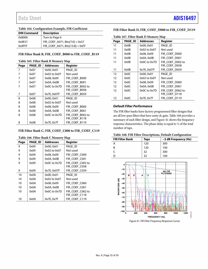
Data Sheet ADIS16497
Rev. A | Page 35 of 39
Table 164. Configuration Example, FIR Coefficient DIN Command Description 0x8006 Turn to Page 6
0x9E57 FIR_COEF_A071, Bits[7:0] = 0x57 0x9FFF FIR_COEF_A071, Bits[15:8] = 0xFF
FIR Filter Bank B, FIR_COEF_B000 to FIR_COEF_B119
Table 165. Filter Bank B Memory Map Page PAGE_ID Addresses Register 7 0x07 0x00, 0x01 PAGE_ID 7 0x07 0x02 to 0x07 Not used 7 0x07 0x08, 0x09 FIR_COEF_B000 7 0x07 0x0A, 0x0B FIR_COEF_B001 7 0x07 0x0C to 0x7D FIR_COEF_B002 to
FIR_COEF_B058 7 0x07 0x7E, 0x07F FIR_COEF_B059 8 0x08 0x00, 0x01 PAGE_ID 8 0x08 0x02 to 0x07 Not used 8 0x08 0x08, 0x09 FIR_COEF_B060 8 0x08 0x0A, 0x0B FIR_COEF_B061 8 0x08 0x0C to 0x7D FIR_COEF_B062 to
FIR_COEF_B118 8 0x08 0x7E, 0x7F FIR_COEF_B119
FIR Filter Bank C, FIR_COEF_C000 to FIR_COEF_C119
Table 166. Filter Bank C Memory Map Page PAGE_ID Addresses Register 9 0x09 0x00, 0x01 PAGE_ID 9 0x09 0x02 to 0x07 Not used 9 0x09 0x08, 0x09 FIR_COEF_C000 9 0x09 0x0A, 0x0B FIR_COEF_C001 9 0x09 0x0C to 0x7D FIR_COEF_C002 to
FIR_COEF_C058 9 0x09 0x7E, 0x07F FIR_COEF_C059 10 0x0A 0x00, 0x01 PAGE_ID 10 0x0A 0x02 to 0x07 Not used 10 0x0A 0x08, 0x09 FIR_COEF_C060 10 0x0A 0x0A, 0x0B FIR_COEF_C061 10 0x0A 0x0C to 0x7D FIR_COEF_C062 to
FIR_COEF_C118 10 0x0A 0x7E, 0x7F FIR_COEF_C119
FIR Filter Bank D, FIR_COEF_D000 to FIR_COEF_D119
Table 167. Filter Bank D Memory Map Page PAGE_ID Addresses Register 11 0x0B 0x00, 0x01 PAGE_ID 11 0x0B 0x02 to 0x07 Not used 11 0x0B 0x08, 0x09 FIR_COEF_D000 11 0x0B 0x0A, 0x0B FIR_COEF_D001 11 0x0B 0x0C to 0x7D FIR_COEF_D002 to
FIR_COEF_D058 11 0x0B 0x7E, 0x07F FIR_COEF_D059 12 0x0C 0x00, 0x01 PAGE_ID 12 0x0C 0x02 to 0x07 Not used 12 0x0C 0x08, 0x09 FIR_COEF_D060 12 0x0C 0x0A, 0x0B FIR_COEF_D061 12 0x0C 0x0C to 0x7D FIR_COEF_D062 to
FIR_COEF_D118 12 0x0C 0x7E, 0x7F FIR_COEF_D119
Default Filter Performance
The FIR filter banks have factory programmed filter designs that are all low-pass filters that have unity dc gain. Table 168 provides a summary of each filter design, and Figure 41 shows the frequency response characteristics. The phase delay is equal to ½ of the total number of taps.
Table 168. FIR Filter Descriptions, Default Configuration FIR Filter Bank Taps −3 dB Frequency (Hz) A 120 300B 120 100C 32 300D 32 100
NO FIRFILTERING
0
–10
–20
MA
GN
ITU
DE
(d
B) –30
–40
–50
–60
–70
–80
–90
–1000 200 400 600 800 1000 1200
FREQUENCY (Hz)
AD CB
1506
1-04
1
Figure 41. FIR Filter Frequency Response Curves

ADIS16497 Data Sheet
Rev. A | Page 36 of 39
FIRMWARE REVISION, FIRM_REV The FIRM_DM register (see Table 171 and Table 172) contains the month and day of the factory configuration date. Register FIRM_DM, Bits[15:12] and Register FIRM_DM, Bits[11:8] contain digits that represent the month of the factory configuration in a binary coded decimal (BCD) format. For example, November is the 11th month in a year and is repre-sented by Register FIRM_DM, Bits[15:8] = 0x11. Register FIRM_DM, Bits[7:4] and Register FIRM_DM, Bits[3:0], contain digits that represent the day of factory configuration in a BCD format. For example, the 27th day of the month is represented by FIRM_DM, Bits[7:0] = 0x27.
Table 169. FIRM_REV Register Definitions Page Addresses Default Access Flash Backup 0x03 0x78, 0x79 Not applicable R Yes
Table 170. FIRM_REV Bit Descriptions Bits Description [15:12] Firmware revision BCD code, tens digit, numerical format
= 4-bit binary, range = 0 to 9 [11:8] Firmware revision BCD code, ones digit, numerical
format = 4-bit binary, range = 0 to 9 [7:4] Firmware revision BCD code, tenths digit, numerical
format = 4-bit binary, range = 0 to 9 [3:0] Firmware revision BCD code, hundredths digit,
numerical format = 4-bit binary, range = 0 to 9
Table 171. FIRM_DM Register Definitions Page Addresses Default Access Flash Backup 0x03 0x7A, 0x7B Not applicable R Yes
Table 172. FIRM_DM Bit Descriptions Bits Description [15:12] Factory configuration month BCD code, tens digit,
numerical format = 4-bit binary, range = 0 to 2 [11:8] Factory configuration month BCD code, ones digit,
numerical format = 4-bit binary, range = 0 to 9 [7:4] Factory configuration day BCD code, tens digit,
numerical format = 4-bit binary, range = 0 to 3 [3:0] Factory configuration day BCD code, ones digit,
numerical format = 4-bit binary, range = 0 to 9
FIRMWARE REVISION YEAR, FIRM_Y The FIRM_Y register (see Table 173 and Table 174) contains the year of the factory configuration date. For example, the year 2013 is represented by FIRM_Y = 0x2013.
Table 173. FIRM_Y Register Definitions Page Addresses Default Access Flash Backup 0x03 0x7C, 0x7D Not applicable R Yes
Table 174. FIRM_Y Bit Descriptions Bits Description [15:12] Factory configuration year BCD code, thousands digit,
numerical format = 4-bit binary, range = 0 to 9 [11:8] Factory configuration year BCD code, hundreds digit,
numerical format = 4-bit binary, range = 0 to 9 [7:4] Factory configuration year BCD code, tens digit,
numerical format = 4-bit binary, range = 0 to 3 [3:0] Factory configuration year BCD code, ones digit,
numerical format = 4-bit binary, range = 0 to 9
BOOT REVISION NUMBER, BOOT_REV
Table 175. BOOT_REV Register Definitions Page Addresses Default Access Flash Backup 0x03 0x7E, 0x7F Not applicable R Yes
Table 176. BOOT_REV Bit Definitions Bits Description [15:8] Binary, major revision number [7:0] Binary, minor revision number
CONTINUOUS SRAM TESTING This device employs a CRC function on the SRAM memory blocks that contain the program code (CODE_SIGTR_xxx) and the calibration coefficients (CAL_DRVTN_xxx). This process operates in the background and generates real-time, 32-bit CRC values for the program code and calibration coefficients, respectively. At the conclusion of each cycle, the processor writes these calculated values in the CAL_DRVTN_xxx and CODE_DRVTN_xxx registers (see Table 183, Table 184, Table 190, and Table 192) and compares them with the signature values, which reflect the state of these memory locations at the time of factory configuration. When the calculation results do not match the signature values, Register SYS_E_FLAG, Bit 2 increases to a 1. The respective signature values are available for user access through the CAL_SIGTR_xxx and CODE_SIGTR_xxx registers (see Table 177, Table 178, Table 179, Table 180, Table 186, and Table 188). The following conditions must be met for Register SYS_E_FLAG, Bit 2 to remain at the zero level:
• CAL_SIGTR_LWR = CAL_DRVTN_LWR• CAL_SIGTR_UPR = CAL_DRVTN_UPR• CODE_SIGTR_LWR = CODE_DRVTN_LWR• CODE_SIGTR_UPR = CODE_DRVTN_UPR
Data Sheet ADIS16497
Rev. A | Page 37 of 39
Signature CRC, Calibration Values, CAL_SIGTR_LWR
Table 177. CAL_SIGTR_LWR Register Definitions Page Addresses Default Access Flash Backup 0x04 0x04, 0x05 Not applicable R Yes
Table 178. CAL_SIGTR_LWR Bit Descriptions Bits Description [15:0] Factory programmed CRC value for the program code,
low word
Signature CRC, Calibration Values, CAL_SIGTR_UPR
Table 179. CAL_SIGTR_UPR Register Definitions Page Addresses Default Access Flash Backup 0x04 0x06, 0x07 Not applicable R Yes
Table 180. CAL_SIGTR_UPR Bit Descriptions Bits Description [15:0] Factory programmed CRC value for the program code,
high word
Derived CRC, Calibration Values, CAL_DRVTN_LWR
Table 181. CAL_DRVTN_LWR Register Definitions Page Addresses Default Access Flash Backup 0x04 0x08, 0x09 Not applicable R No
Table 182. CAL_DRVTN_LWR Bit Descriptions Bits Description [15:0] Calculated CRC value for the program code, low word
Derived CRC, Calibration Values, CAL_DRVTN_UPR
Table 183. CAL_DRVTN_UPR Register Definitions Page Addresses Default Access Flash Backup 0x04 0x0A, 0x0B Not applicable R No
Table 184. CAL_DRVTN_UPR Bit Descriptions Bits Description [15:0] Calculated CRC value for the program code, high word
Signature CRC, Program Code, CODE_SIGTR_LWR
Table 185. CODE_SIGTR_LWR Register Definitions Page Addresses Default Access Flash Backup 0x04 0x0C, 0x0D Not applicable R Yes
Table 186. CODE_SIGTR_LWR Bit Descriptions Bits Description [15:0] Factory programmed CRC value for the calibration
coefficients, low word
Signature CRC, Program Code, CODE_SIGTR_UPR
Table 187. CODE_SIGTR_UPR Register Definitions Page Addresses Default Access Flash Backup 0x04 0x0E, 0x0F Not applicable R Yes
Table 188. CODE_SIGTR_UPR Bit Descriptions Bits Description [15:0] Factory programmed CRC value for the calibration
coefficients, high word
Derived CRC, Program Code, CODE_DRVTN_LWR
Table 189. CODE_DRVTN_LWR Register Definitions Page Addresses Default Access Flash Backup 0x04 0x10, 0x11 Not applicable R No
Table 190. CODE_DRVTN_LWR Bit Descriptions Bits Description [15:0] Calculated CRC value for the calibration coefficients, low
word
Derived CRC, Program Code, CODE_DRVTN_UPR
Table 191. CODE_DRVTN_LWR Register Definitions Page Addresses Default Access Flash Backup 0x04 0x12, 0x13 Not applicable R No
Table 192. CODE_DRVTN_UPR Bit Descriptions Bits Description [15:0] Calculated CRC value for the calibration coefficients,
high word
Lot Specific Serial Number, SERIAL_NUM
Table 193. SERIAL_NUM Register Definitions Page Addresses Default Access Flash Backup 0x04 0x20, 0x21 Not applicable R Yes
Table 194. SERIAL_NUM Bit Descriptions Bits Description [15:0] Lot specific serial number

ADIS16497 Data Sheet
Rev. A | Page 38 of 39
APPLICATIONS INFORMATION MOUNTING BEST PRACTICES For the best performance, follow these guidelines when installing the ADIS16497 into a system:
Eliminate opportunity for translational force (x- and y-axis direction, per Figure 31) application on the electrical connector.
Use uniform mounting forces on all four corners. Thesuggested torque setting is 40 inch ounces (0.285 Nm).
When the ADIS16497 rests on the PCB, which contains themating connector (see Figure 42), use a diameter of at least2.85 mm for the passthrough holes.
These guidelines help prevent irregular force profiles, which can warp the package and introduce bias errors in the sensors. Figure 42 and Figure 43 provide details for mounting hole and connector alignment pin drill locations.
DEVICEOUTLINE
19.800 BSC
39.600 BSC
42.6
0021
.300
BS
C
5 BSC5 BSC
1.64
2 B
SC
NOTES1. ALL DIMENSIONS IN UNITS OF MILLIMETERS (mm).2. IN THIS CONFIGURATION, THE CONNECTOR IS FACING DOWN AND
ITS PINSARE NOT VISIBLE.
0.560 BSC 2×ALIGNMENT HOLES
PASSTHROUGH HOLEFOR MOUNTING SCREWS
DIAMETER OF THE HOLEMUST ACCOMODATEDIMENSIONAL TOLERANCEBETWEEN THE CONNECTORAND HOLES
FOR MATING SOCKET
1506
1-04
2
Figure 42. Suggested PCB Layout Pattern, Connector Down
0.4334 [11.0]
0.0240 [0.610]0.019685[0.5000](TYP)
0.054 [1.37]
0.0394 [1.00]
0.0394 [1.00] 0.1800[4.57]
NONPLATEDTHROUGH HOLE 2×
0.022± DIA (TYP)
0.022 DIA THROUGH HOLE (TYP)NONPLATED THROUGH HOLE 15
061-
043
Figure 43. Suggested Layout and Mechanical Design When Using Samtec CLM-112-02-G-D-A for the Mating Connector
PREVENTING MISINSERTION The ADIS16497 connector uses the same pattern as the ADIS16485, but with Pin 12 and Pin 15 missing. This pin configuration enables a mating connector to plug these holes, which helps prevent misconnection with the ADIS16497. Samtec has a custom part number that provides this type of mating socket: ASP-193371-04.
EVALUATION TOOLS Breakout Board, ADIS16IMU1/PCBZ
The ADIS16IMU1/PCBZ (sold separately) provides a breakout board function for the ADIS16497, which means that it provides access to the ADIS16497 through larger connectors that support standard 1 mm ribbon cabling. It also provides four mounting holes for attachment of the ADIS16497 to the breakout board.
PC-Based Evaluation, EVAL-ADIS2
Use the EVAL-ADIS2 and ADIS16IMU1/PCBZ to evaluate the ADIS16497 on a PC-based platform.
POWER SUPPLY CONSIDERATIONS The VDD power supply must charge 46 μF of capacitance (inside of the ADIS16497, across the VDD and GND pins) during its initial ramp and settling process. When VDD reaches 2.85 V, the ADIS16497 begins its internal start-up process, which gener-ates additional transient current demand. See Figure 44 for a typical current profile during the start-up process. The first peak in Figure 44 relates to charging the 46 μF capacitor bank, whereas the other transient activity relates to numerous functions turning on during the initialization process of the ADIS16497.
CH2 2.0V BW
CH3 2.0V BW CH4 100mA B
W
M40.0ms A CH3 3.00VT 20.10% 12.5MS/s 5M pts
4
3
2DR
VDD
CURRENT
a bT a
b
1.608ms
159.8ms
92.00mA
152.0mA∆158.2ms ∆60.00mA
1506
1-04
4
Figure 44. Transient Current Demand, Startup

Data Sheet ADIS16497
Rev. A | Page 39 of 39
OUTLINE DIMENSIONS
02-2
2-20
17-A
BOTTOM VIEW
FRONT VIEW
TOP VIEW
44.25444.00043.746
34.60034.57534.550
39.80039.60039.400 20.00
19.8019.60
47.25447.00046.746
37.59837.57337.548
42.80042.60042.400
2.20 BSC
Ø 2.40BSC
2.20 BSC
14.20014.00013.800
3.4543.2002.946
0.250 BSC
13.750 REF 0.250 BSC
5.50BSC
5.50BSC
DETAIL A
DETAIL A
1.00 BSCPITCH 0.30 SQ BSC
1.142 BSC
Ø2.0652.0402.015
2.0652.0402.015
47.479°
47.37947.279
3.703.503.30
7.3507.2257.100
2.3252.2002.075
2.84 BSC
Figure 45. 24-Lead Module with Connector Interface [MODULE] (ML-24-9)
Dimensions shown in millimeters
ORDERING GUIDE Model1 Temperature Range Description Package Option ADIS16497-1BMLZ −40°C to +105°C 24-Lead Module with Connector Interface [MODULE] ML-24-9 ADIS16497-2BMLZ −40°C to +105°C 24-Lead Module with Connector Interface [MODULE] ML-24-9 ADIS16497-3BMLZ −40°C to +105°C 24-Lead Module with Connector Interface [MODULE] ML-24-9
1 Z = RoHS Compliant Part.
©2017 Analog Devices, Inc. All rights reserved. Trademarks and registered trademarks are the property of their respective owners.
D15061-0-11/17(0)