Compact, Precision, Six Degrees of Freedom Inertial … Precision, Six Degrees of Freedom Inertial...
26
Compact, Precision, Six Degrees of Freedom Inertial Sensor Data Sheet ADIS16460 Rev. B Document Feedback Information furnished by Analog Devices is believed to be accurate and reliable. However, no responsibility is assumed by Analog Devices for its use, nor for any infringements of patents or other rights of third parties that may result from its use. Specifications subject to change without notice. No license is granted by implication or otherwise under any patent or patent rights of Analog Devices. Trademarks and registered trademarks are the property of their respective owners. One Technology Way, P.O. Box 9106, Norwood, MA 02062-9106, U.S.A. Tel: 781.329.4700 ©2016–2017 Analog Devices, Inc. All rights reserved. Technical Support www.analog.com FEATURES Triaxial digital gyroscope Measurement range: ±100°/sec (minimum) 8°/hr (typical) in-run bias stability 0.12°/√hr (typical) angle random walk, x-axis Triaxial digital accelerometer, ±5 g dynamic range Autonomous operation and data collection No external configuration commands required Fast start-up time Factory calibrated sensitivity, bias, and axial alignment Calibration temperature range: 0°C ≤ TA ≤ 70°C Serial peripheral interface (SPI) data communications Data ready signal for synchronizing data acquisition Embedded temperature sensor Programmable operation and control Automatic and manual bias correction controls Bartlett window finite impulse response (FIR) filter, variable number of taps External sample clock options: direct Single command self test Single-supply operation: 3.15 V to 3.45 V 2000 g shock survivability Operating temperature range: −25°C to +85°C APPLICATIONS Smart agriculture/construction machinery Unmanned aerial vehicles (UAVs)/drones, and navigation and payload stabilization Robotics Factory/industrial automation personnel/asset tracking GENERAL DESCRIPTION The ADIS16460 iSensor® device is a complete inertial system that includes a triaxial gyroscope and a triaxial accelerometer. Each sensor in the ADIS16460 combines industry leading iMEMS® technology with signal conditioning that optimizes dynamic performance. The factory calibration characterizes each sensor for sensitivity, bias, and alignment. As a result, each sensor has its own dynamic compensation formulas that provide accurate sensor measurements. The ADIS16460 provides a simple, cost effective method for integrating accurate, multiaxis inertial sensing into industrial systems, especially when compared with the complexity and investment associated with discrete designs. All necessary motion testing and calibration are part of the production process at the factory, greatly reducing system integration time. Tight orthogonal alignment simplifies inertial frame alignment in navigation systems. The SPI and register structures provide a simple interface for data collection and configuration control. The ADIS16460 is in an aluminum module package that is approximately 22.4 mm × 22.4 mm × 9 mm and has a 14-pin connector interface. FUNCTIONAL BLOCK DIAGRAM CONTROLLER CLOCK TRIAXIAL GYROSCOPE TRIAXIAL ACCELEROMETER POWER MANAGEMENT CS SCLK DIN DOUT GND VDD TEMPERATURE DR SYNC RST SPI SELF TEST I/O ALARMS OUTPUT DATA REGISTERS USER CONTROL REGISTERS CALIBRATION AND FILTERS ADIS16460 13390-001 Figure 1.
Transcript of Compact, Precision, Six Degrees of Freedom Inertial … Precision, Six Degrees of Freedom Inertial...

Compact, Precision, Six Degrees of Freedom Inertial Sensor
Data Sheet ADIS16460
Rev. B Document Feedback Information furnished by Analog Devices is believed to be accurate and reliable. However, no responsibility is assumed by Analog Devices for its use, nor for any infringements of patents or other rights of third parties that may result from its use. Specifications subject to change without notice. No license is granted by implication or otherwise under any patent or patent rights of Analog Devices. Trademarks and registered trademarks are the property of their respective owners.
One Technology Way, P.O. Box 9106, Norwood, MA 02062-9106, U.S.A. Tel: 781.329.4700 ©2016–2017 Analog Devices, Inc. All rights reserved. Technical Support www.analog.com
FEATURES Triaxial digital gyroscope
Measurement range: ±100°/sec (minimum) 8°/hr (typical) in-run bias stability 0.12°/√hr (typical) angle random walk, x-axis
Triaxial digital accelerometer, ±5 g dynamic range Autonomous operation and data collection
No external configuration commands required Fast start-up time
Factory calibrated sensitivity, bias, and axial alignment Calibration temperature range: 0°C ≤ TA ≤ 70°C
Serial peripheral interface (SPI) data communications Data ready signal for synchronizing data acquisition Embedded temperature sensor Programmable operation and control
Automatic and manual bias correction controls Bartlett window finite impulse response (FIR) filter, variable number of taps External sample clock options: direct Single command self test
Single-supply operation: 3.15 V to 3.45 V 2000 g shock survivability Operating temperature range: −25°C to +85°C
APPLICATIONS Smart agriculture/construction machinery Unmanned aerial vehicles (UAVs)/drones, and navigation
and payload stabilization Robotics Factory/industrial automation personnel/asset tracking
GENERAL DESCRIPTION The ADIS16460 iSensor® device is a complete inertial system that includes a triaxial gyroscope and a triaxial accelerometer. Each sensor in the ADIS16460 combines industry leading iMEMS® technology with signal conditioning that optimizes dynamic performance. The factory calibration characterizes each sensor for sensitivity, bias, and alignment. As a result, each sensor has its own dynamic compensation formulas that provide accurate sensor measurements.
The ADIS16460 provides a simple, cost effective method for integrating accurate, multiaxis inertial sensing into industrial systems, especially when compared with the complexity and investment associated with discrete designs. All necessary motion testing and calibration are part of the production process at the factory, greatly reducing system integration time. Tight orthogonal alignment simplifies inertial frame alignment in navigation systems. The SPI and register structures provide a simple interface for data collection and configuration control.
The ADIS16460 is in an aluminum module package that is approximately 22.4 mm × 22.4 mm × 9 mm and has a 14-pin connector interface.
FUNCTIONAL BLOCK DIAGRAM
CONTROLLER
CLOCK
TRIAXIALGYROSCOPE
TRIAXIALACCELEROMETER
POWERMANAGEMENT
CS
SCLK
DIN
DOUT
GND
VDD
TEMPERATURE
DR SYNC RST
SPI
SELF TEST I/O ALARMS
OUTPUTDATA
REGISTERS
USERCONTROL
REGISTERS
CALIBRATIONAND
FILTERS
ADIS16460
1339
0-00
1
Figure 1.
ADIS16460 Data Sheet
Rev. B | Page 2 of 26
TABLE OF CONTENTS Features .............................................................................................. 1 Applications ....................................................................................... 1 General Description ......................................................................... 1 Functional Block Diagram .............................................................. 1 Revision History ............................................................................... 2 Specifications ..................................................................................... 3
Timing Specifications .................................................................. 5 Absolute Maximum Ratings ............................................................ 6
ESD Caution .................................................................................. 6 Pin Configuration and Function Descriptions ............................. 7 Typical Performance Characteristics ............................................. 8 Theory of Operation ...................................................................... 10
Reading Sensor Data .................................................................. 10 Device Configuration ................................................................ 11
User Registers .................................................................................. 12 Output Data Registers .................................................................... 13
Rotation ....................................................................................... 13 Accelerometers ............................................................................ 15 Internal Temperature ................................................................. 17 Product Identification ................................................................ 17 Status/Error Flags ....................................................................... 17
System Functions ............................................................................ 19
Global Commands ..................................................................... 19 Software Reset ............................................................................. 19 Flash Memory Test ..................................................................... 19 Manual Flash Update ................................................................. 19 Automated Self Test ................................................................... 19 Input/Output Configuration ..................................................... 19 Data Ready (DR) Pin Configuration ....................................... 19 SYNC Pin Configuration .......................................................... 20
Digital Processing Configuration ................................................. 21 Gyroscopes/Accelerometers ..................................................... 21
Calibration ....................................................................................... 22 Gyroscopes .................................................................................. 22 Accelerometers ........................................................................... 22 Restoring Factory Calibration .................................................. 23
Applications Information .............................................................. 24 Mounting Tips ............................................................................ 24 Power Supply Considerations ................................................... 24 Breakout Board ........................................................................... 24 PC-Based Evaluation Tools ....................................................... 25
Outline Dimensions ....................................................................... 26 Ordering Guide .......................................................................... 26
REVISION HISTORY 6/2017—Rev. A to Rev. B Changed ML-14-5 to ML-14-6 ......................................... Universal Change to Gryoscope/Misalignment/Axis to Axis Parameter, Table 1 ................................................................................................ 3 Changes to Figure 6 .......................................................................... 7 Changes to Figure 26 ...................................................................... 13 Changes to Figure 28 ...................................................................... 15 Changes to Figure 32 ...................................................................... 23 Updated Outline Dimensions ....................................................... 26 Changes to Ordering Guide .......................................................... 26
8/2016—Rev. 0 to Rev. A Changes to Features Section ............................................................ 1 Changes to Table 1 ............................................................................. 3 Changes to tNV Parameter, Table 2 ................................................... 5 Changed Acceleration (Shock) Parameter to Mechanical Shock Survival Parameter, Table 3 .............................................................. 6 Changes to Burst Read Function Section and Figure 21 ........... 11 Change to Bit 7, Table 44 ............................................................... 19 1/2016—Revision 0: Initial Version
Data Sheet ADIS16460
Rev. B | Page 3 of 26
SPECIFICATIONS TA = 25°C, VDD = 3.3 V, angular rate = 0°/sec, ± 1 g, MSC_CTRL = 0x00C1, unless otherwise noted.
Table 1. Parameter Test Conditions/Comments Min Typ Max Unit GYROSCOPES
Dynamic Range ±100 °/sec Initial Sensitivity 16-bit data format1 0.005 °/sec/LSB 32-bit data format1 7.63 × 10⁻⁸ °/sec/LSB
Repeatability2 0°C ≤ TA ≤ 70°C 1 % Sensitivity Temperature Coefficient 0°C ≤ TA ≤ 70°C ±20 ppm/°C Misalignment Axis to axis ±0.05 Degrees Axis to frame (package) ±1 Degrees Nonlinearity Best fit straight line 0.5 % of FS Bias Repeatability2, 3 0°C ≤ TA ≤ 70°C, 1 σ 0.5 °/sec In-Run Bias Stability 1 σ 8 °/hr Angle Random Walk 1 σ, x-axis 0.12 °/√hr 1 σ, y-axis, z-axis 0.17 °/√hr Bias Temperature Coefficient 0°C ≤ TA ≤ 70°C ±0.007 °/sec/°C Linear Acceleration Effect on Bias Any axis, 1 σ ±0.01 °/sec/g Vibration Rectification Error 20 Hz to 2000 Hz, 5 g rms ±0.0004 °/sec/g2 Bias Supply Sensitivity 3.15 V ≤ VDD ≤ 3.45 V 0.037 °/sec/V Output Noise No filtering 0.075 °/sec rms Rate Noise Density 10 Hz to 40 Hz, no filtering 0.004 °/sec/√Hz rms −3 dB Bandwidth 375 Hz Sensor Resonant Frequency 65 kHz
ACCELEROMETERS Each axis Dynamic Range ±5 g Initial Sensitivity 16-bit data format4 0.25 mg/LSB 32-bit data format4 3.81 × 10⁻⁶ mg/LSB
Repeatability2 0°C ≤ TA ≤ 70°C 1 % Sensitivity Temperature Coefficient 0°C ≤ TA ≤ 70°C ±15 ppm/°C Misalignment Axis to axis ±0.05 Degrees Axis to frame (package) ±1 Degrees Nonlinearity Best fit straight line ±0.1 % of FS Bias Repeatability2, 3 0°C ≤ TA ≤ +70°C, 1 σ ±15 mg In-Run Bias Stability 1 σ 0.2 mg Velocity Random Walk 1 σ 0.09 m/sec/√hr Bias Temperature Coefficient 0°C ≤ TA ≤ 70°C ±0.05 mg/°C Vibration Rectification Error 20 Hz to 2000 Hz, 1 g rms 0.08 mg/g2 Bias Supply Sensitivity 3.15 V ≤ VDD ≤ 3.45 V 72 mg/V Output Noise No filtering 4.5 mg rms Noise Density 10 Hz to 40 Hz, no filtering 0.2 mg/√Hz rms −3 dB Bandwidth 350 Hz Sensor Resonant Frequency 5.5 kHz
TEMPERATURE Sensitivity See Table 37 0.05 °C/LSB
LOGIC INPUTS5 Input High Voltage, VIH 2.0 V Input Low Voltage, VIL 0.8 V Logic 1 Input Current, IIH VIH = 3.3 V ±0.2 ±10 µA
ADIS16460 Data Sheet
Rev. B | Page 4 of 26
Parameter Test Conditions/Comments Min Typ Max Unit Logic 0 Input Current, IIL VIL = 0 V
All Pins Except RST 40 60 µA
RST Pin 1 mA
Input Capacitance, CIN 10 pF DIGITAL OUTPUTS5
Output High Voltage, VOH ISOURCE = 1.6 mA 2.4 V Output Low Voltage, VOL ISINK = 1.6 mA 0.4 V
FLASH MEMORY Endurance6 10,000 Cycles Data Retention7 TJ = 85°C 20 Years
FUNCTIONAL TIMES8 Time until new data is available Power-On Start-Up Time 290 ms Reset Recovery Time9, 10 222 ms Reset Initiation Time11 10 μs
CONVERSION RATE x_GYRO_OUT, x_ACCL_OUT 2048 SPS Clock Accuracy ±3 % Sync Input Clock12 MSC_CTRL[3:2] = 01 0.8 2000 Hz PPS Input Clock MSC_CTRL[3:2] = 10 128 Hz
POWER SUPPLY Operating voltage range, VDD 3.15 3.3 3.45 V Power Supply Current VDD = 3.15 V 44 55 mA
1 The X_GYRO_LOW (see Table 10), Y_GYRO_LOW (see Table 12), and Z_GYRO_LOW (see Table 14) registers capture the bit growth associated with the user
configurable filters. 2 The repeatability specifications represent analytical projections, which are based on the following drift contributions and conditions: temperature hysteresis (0°C to
70°C), electronics drift (high temperature operating life test: 85°C, 500 hours), drift from temperature cycling (JESD22, Method A104-C, Method N, 500 cycles, −40°C to +85°C), rate random walk (10 year projection), and broadband noise.
3 Bias repeatability describes a long-term behavior, over a variety of conditions. Short-term repeatability is related to the in-run bias stability and noise density specifications.
4 The X_ACCL_LOW (see Table 24), Y_ACCL_LOW (see Table 26), and Z_ACCL_LOW (see Table 28) registers capture the bit growth associated with the user configurable filters.
5 The digital I/O signals are driven by an internal 3.3 V supply, and the inputs are 5 V tolerant. 6 Endurance is qualified as per JEDEC Standard 22, Method A117, and measured at −40°C, +25°C, +85°C, and +125°C. 7 The data retention lifetime equivalent is at a junction temperature (TJ) of 85°C as per JEDEC Standard 22, Method A117. Data retention lifetime decreases with junction
temperature. 8 These times do not include thermal settling and internal filter response times (375 Hz bandwidth), which may affect overall accuracy. 9 The parameter assumes that a full start-up sequence has taken place, prior to initiation of the reset cycle. 10 This parameter represents the time between raising the RST line and restoration of pulsing on the DR line, which indicates a return to normal operation. 11 This parameter represents the pulse time on the RST line, which ensures initiation of the reset operation. 12 The sync input clock functions below the specified minimum value but at reduced performance levels.
Data Sheet ADIS16460
Rev. B | Page 5 of 26
TIMING SPECIFICATIONS TA = 25°C, VDD = 3.3 V, unless otherwise noted.
Table 2.
Parameter Description Normal Mode Burst Read
Unit Min1 Typ Max Min1 Typ Max fSCLK Serial clock 0.1 2.0 0.1 1.0 MHz tSTALL Stall period between data 16 N/A2 µs tREADRATE Read rate 24 µs tCS Chip select to SCLK edge 200 200 ns tDAV DOUT valid after SCLK edge 25 25 ns tDSU DIN setup time before SCLK rising edge 25 25 ns tDHD DIN hold time after SCLK rising edge 50 50 ns tSCLKR, tSCLKF SCLK rise/fall times 5 12.5 5 12.5 ns tDR, tDF DOUT rise/fall times 5 12.5 5 12.5 ns tSFS CS high after SCLK edge 0 0 ns
t1 Input sync positive pulse width 25 25 µs tSTDR Input sync to data ready valid transition 636 636 µs tNV Data invalid time 47 47 µs t2 Input sync period 500 500 µs 1 Guaranteed by design and characterization, but not tested in production. 2 When using the burst read mode, the stall period is not applicable.
Timing Diagrams
CS
SCLK
DOUT
DIN
1 2 3 4 5 6 15 16
R/W A5A6 A4 A3 A2 DC2
MSB D14
DC1 LSB
D13 D12 D10D11 D2 LSBD1
tCS tSFS
tDAV
tDHDtDSU
tSCLKR
tDR
tDF
tSCLKF
1339
0-00
2
Figure 2. SPI Timing and Sequence
CS
SCLK
tREADRATE
tSTALL
1339
0-00
3
Figure 3. Stall Time and Data Rate
CLOCK
DATAREADY
t1
t2
tNV
tSTDR
1339
0-00
4
Figure 4. Input Clock Timing Diagram, MSC_CTRL[0] = 1
ADIS16460 Data Sheet
Rev. B | Page 6 of 26
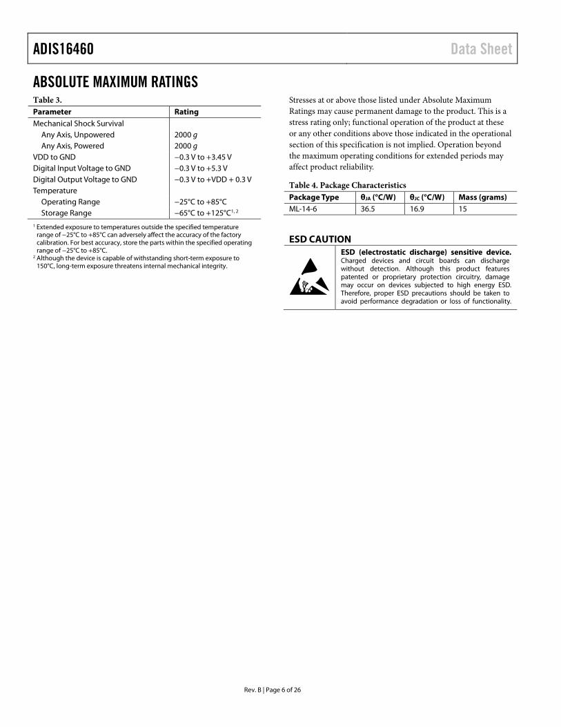
ABSOLUTE MAXIMUM RATINGS Table 3. Parameter Rating Mechanical Shock Survival
Any Axis, Unpowered 2000 g Any Axis, Powered 2000 g
VDD to GND −0.3 V to +3.45 V Digital Input Voltage to GND −0.3 V to +5.3 V Digital Output Voltage to GND −0.3 V to +VDD + 0.3 V Temperature
Operating Range −25°C to +85°C Storage Range −65°C to +125°C1, 2
1 Extended exposure to temperatures outside the specified temperature
range of −25°C to +85°C can adversely affect the accuracy of the factory calibration. For best accuracy, store the parts within the specified operating range of −25°C to +85°C.
2 Although the device is capable of withstanding short-term exposure to 150°C, long-term exposure threatens internal mechanical integrity.
Stresses at or above those listed under Absolute Maximum Ratings may cause permanent damage to the product. This is a stress rating only; functional operation of the product at these or any other conditions above those indicated in the operational section of this specification is not implied. Operation beyond the maximum operating conditions for extended periods may affect product reliability.
Table 4. Package Characteristics Package Type θJA (°C/W) θJC (°C/W) Mass (grams) ML-14-6 36.5 16.9 15
ESD CAUTION
Data Sheet ADIS16460
Rev. B | Page 7 of 26
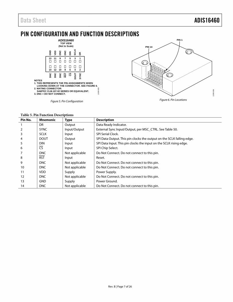
PIN CONFIGURATION AND FUNCTION DESCRIPTIONS
SYN
C
DO
UT
CS
RST
DN
CD
NC
DN
C
DR
SCLK
DIN
DN
C
DN
CVD
D
GN
D
13
14
11
12
9
10
7
8
5
6
3
4
1
2
ADIS16460TOP VIEW
(Not to Scale)
1339
0-00
5
NOTES1. THIS REPRESENTS THE PIN ASSIGNMENTS WHEN LOOKING DOWN AT THE CONNECTOR. SEE FIGURE 6.2. MATING CONNECTOR: SAMTEC CLM-107-02 SERIES OR EQUIVALENT.3. DNC = DO NOT CONNECT.
Figure 5. Pin Configuration
PIN 1
PIN 14
1339
0-00
6
Figure 6. Pin Locations
Table 5. Pin Function Descriptions Pin No. Mnemonic Type Description 1 DR Output Data Ready Indicator. 2 SYNC Input/Output External Sync Input/Output, per MSC_CTRL. See Table 50. 3 SCLK Input SPI Serial Clock. 4 DOUT Output SPI Data Output. This pin clocks the output on the SCLK falling edge. 5 DIN Input SPI Data Input. This pin clocks the input on the SCLK rising edge. 6 CS Input SPI Chip Select.
7 DNC Not applicable Do Not Connect. Do not connect to this pin. 8 RST Input Reset.
9 DNC Not applicable Do Not Connect. Do not connect to this pin. 10 DNC Not applicable Do Not Connect. Do not connect to this pin. 11 VDD Supply Power Supply. 12 DNC Not applicable Do Not Connect. Do not connect to this pin. 13 GND Supply Power Ground. 14 DNC Not applicable Do Not Connect. Do not connect to this pin.

ADIS16460 Data Sheet
Rev. B | Page 8 of 26
TYPICAL PERFORMANCE CHARACTERISTICS 100
1
10
0.01 0.1 1 10 100 1k 10k
RO
OT
ALL
AN
VA
RIA
NC
E (°
/Hr)
Tau (Seconds) 1339
0-00
7
MEANMEAN + 1σ
MEAN – 1σ
Figure 7. Gyroscope Root Allan Variance
0.5
–0.5
–0.4
–0.3
–0.2
–0.1
0
0.1
0.2
0.3
0.4
–60 –40 –20 0 20 40 60 80 100
GYR
OSC
OPE
SEN
SITI
VITY
ER
RO
R (%
of F
S)
TEMPERATURE (°C) 1339
0-10
0
MEAN + 1σ
MEAN – 1σ
MEAN
Figure 8. Gyroscope Sensitivity Error vs. Cold to Hot Temperature Sweep
2.0
–2.0
–1.5
–1.0
–0.5
0
0.5
1.0
1.5
–60 –40 –20 0 20 40 60 80 100
GYR
OSC
OPE
BIA
S ER
RO
R (°
/sec
)
TEMPERATURE (°C) 1339
0-10
2
MEAN + 1σ
MEAN – 1σ
MEAN
Figure 9. Gyroscope Bias Error vs. Cold to Hot Temperature Sweep
10
0.01
0.1
1
0.01 0.1 1 10 100 1k 10k
RO
OT
ALL
AN
VA
RIA
NC
E (m
g)
Tau (Seconds) 1339
0-00
8
MEAN MEAN + 1σ
MEAN – 1σ
Figure 10. Accelerometer Root Allan Variance
0.5
–0.5
–0.4
–0.3
–0.2
–0.1
0
0.1
0.2
0.3
0.4
–60 –40 –20 0 20 40 60 80 100
GYR
OSC
OPE
SEN
SITI
VITY
ER
RO
R (%
of F
S)
TEMPERATURE (°C) 1339
0-10
1
MEAN + 1σ
MEAN – 1σ
MEAN
Figure 11. Gyroscope Sensitivity Error vs. Hot to Cold Temperature Sweep
2.0
–2.0
–1.5
–1.0
–0.5
0
0.5
1.0
1.5
–60 –40 –20 0 20 40 60 80 100
GYR
OSC
OPE
BIA
S ER
RO
R (°
/sec
)
TEMPERATURE (°C) 1339
0-10
3
MEAN + 1σ
MEAN – 1σ
MEAN
Figure 12. Gyroscope Bias Error vs. Hot to Cold Temperature Sweep
Data Sheet ADIS16460
Rev. B | Page 9 of 26
0.5
–0.5
–0.4
–0.3
–0.2
–0.1
0
0.1
0.2
0.3
0.4
–60 –40 –20 0 20 40 60 80 100
AC
CEL
ERO
MET
ER S
ENSI
TIVI
TY E
RR
OR
(% o
f FS)
TEMPERATURE (°C) 1339
0-10
4
MEAN + 1σ
MEAN – 1σ
MEAN
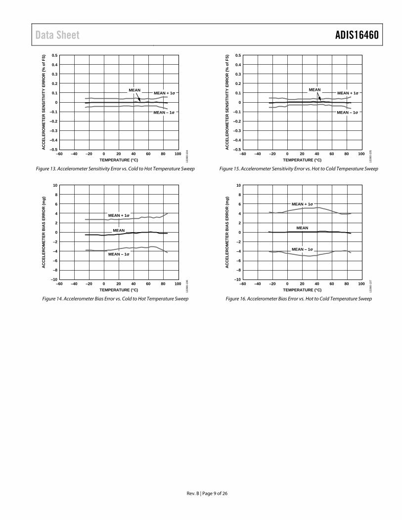
Figure 13. Accelerometer Sensitivity Error vs. Cold to Hot Temperature Sweep
10
–10
–8
–6
–4
–2
0
2
4
6
8
–40 –20–60 0 20 40 60 80 100
AC
CEL
ERO
MET
ER B
IAS
ERR
OR
(mg)
TEMPERATURE (°C) 1339
0-10
6
MEAN + 1σ
MEAN – 1σ
MEAN
Figure 14. Accelerometer Bias Error vs. Cold to Hot Temperature Sweep
0.5
–0.5
–0.4
–0.3
–0.2
–0.1
0
0.1
0.2
0.3
0.4
–60 –40 –20 0 20 40 60 80 100
AC
CEL
ERO
MET
ER S
ENSI
TIVI
TY E
RR
OR
(% o
f FS)
TEMPERATURE (°C) 1339
0-10
5
MEAN + 1σ
MEAN – 1σ
MEAN
Figure 15. Accelerometer Sensitivity Error vs. Hot to Cold Temperature Sweep
10
–10
–8
–6
–4
–2
0
2
4
6
8
–60 –40 –20 0 20 40 60 80 100
AC
CEL
ERO
MET
ER B
IAS
ERR
OR
(mg)
TEMPERATURE (°C) 1339
0-10
7
MEAN + 1σ
MEAN – 1σ
MEAN
Figure 16. Accelerometer Bias Error vs. Hot to Cold Temperature Sweep
ADIS16460 Data Sheet
Rev. B | Page 10 of 26
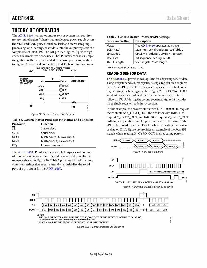
THEORY OF OPERATION The ADIS16460 is an autonomous sensor system that requires no user initialization. When it has an adequate power supply across the VDD and GND pins, it initializes itself and starts sampling, processing, and loading sensor data into the output registers at a sample rate of 2048 SPS. The DR pin (see Figure 5) pulses high after each sample cycle concludes. The SPI interface enables simple integration with many embedded processor platforms, as shown in Figure 17 (electrical connection) and Table 6 (pin functions).
SYSTEMPROCESSORSPI MASTER
ADIS16460SCLK
CS
DIN
DOUT
SCLK
SS
MOSI
MISO
+3.3V
IRQ DR
VDDI/O LINES ARE COMPATIBLE WITH
3.3V LOGIC LEVELS
6
3
5
4
1
11
13
1339
0-00
9
Figure 17. Electrical Connection Diagram
Table 6. Generic Master Processor Pin Names and Functions Pin Name Function SS Slave select
SCLK Serial clock MOSI Master output, slave input MISO Master input, slave output IRQ Interrupt request
The ADIS16460 SPI interface supports full duplex serial commu-nication (simultaneous transmit and receive) and uses the bit sequence shown in Figure 20. Table 7 provides a list of the most common settings that require attention to initialize the serial port of a processor for the ADIS16460.
Table 7. Generic Master Processor SPI Settings Processor Setting Description Master The ADIS16460 operates as a slave SCLK Rate1 Maximum serial clock rate, see Table 2 SPI Mode 3 CPOL = 1 (polarity), CPHA = 1 (phase) MSB First Bit sequence, see Figure 20 16-Bit Length Shift register/data length
1 For burst read, SCLK rate ≤ 1 MHz.
READING SENSOR DATA The ADIS16460 provides two options for acquiring sensor data: a single register and a burst register. A single register read requires two 16-bit SPI cycles. The first cycle requests the contents of a register using the bit assignments in Figure 20. Bit DC7 to Bit DC0 are don’t cares for a read, and then the output register contents follow on DOUT during the second sequence. Figure 18 includes three single register reads in succession.
In this example, the process starts with DIN = 0x0600 to request the contents of X_GYRO_OUT, then follows with 0x0A00 to request Y_GYRO_OUT, and 0x0E00 to request Z_GYRO_OUT. Full duplex operation enables processors to use the same 16-bit SPI cycle to read data from DOUT while requesting the next set of data on DIN. Figure 19 provides an example of the four SPI signals when reading X_GYRO_OUT in a repeating pattern.
X_GYRO_OUT
DIN
DOUT Y_GYRO_OUT Z_GYRO_OUT
0x0600 0x0A00 0x0E00
1339
0-01
0
Figure 18. SPI Read Example
SCLK
CS
DIN
DOUT
DOUT = 1111 1111 1111 1010 = 0xFFFA = –6 LSB = –0.03°/sec
DIN = 0000 0110 0000 0000 = 0x0600
1339
0-01
1
Figure 19. Example SPI Read, Second Sequence
R/W R/WA6 A5 A4 A3 A2 A1 A0 DC7 DC6 DC5 DC4 DC3 DC2 DC1 DC0
D0D1D2D3D4D5D6D7D8D9D10D11D12D13D14D15
CS
SCLK
DIN
DOUT
A6 A5
D13D14D15
NOTES1. THE DOUT BIT PATTERN REFLECTS THE ENTIRE CONTENTS OF THE REGISTER IDENTIFIED BY [A6:A0] IN THE PREVIOUS 16-BIT DIN SEQUENCE WHEN R/W = 0.2. IF R/W = 1 DURING THE PREVIOUS SEQUENCE, DOUT IS NOT DEFINED. 13
390-
012
Figure 20. SPI Communication Bit Sequence
Data Sheet ADIS16460
Rev. B | Page 11 of 26
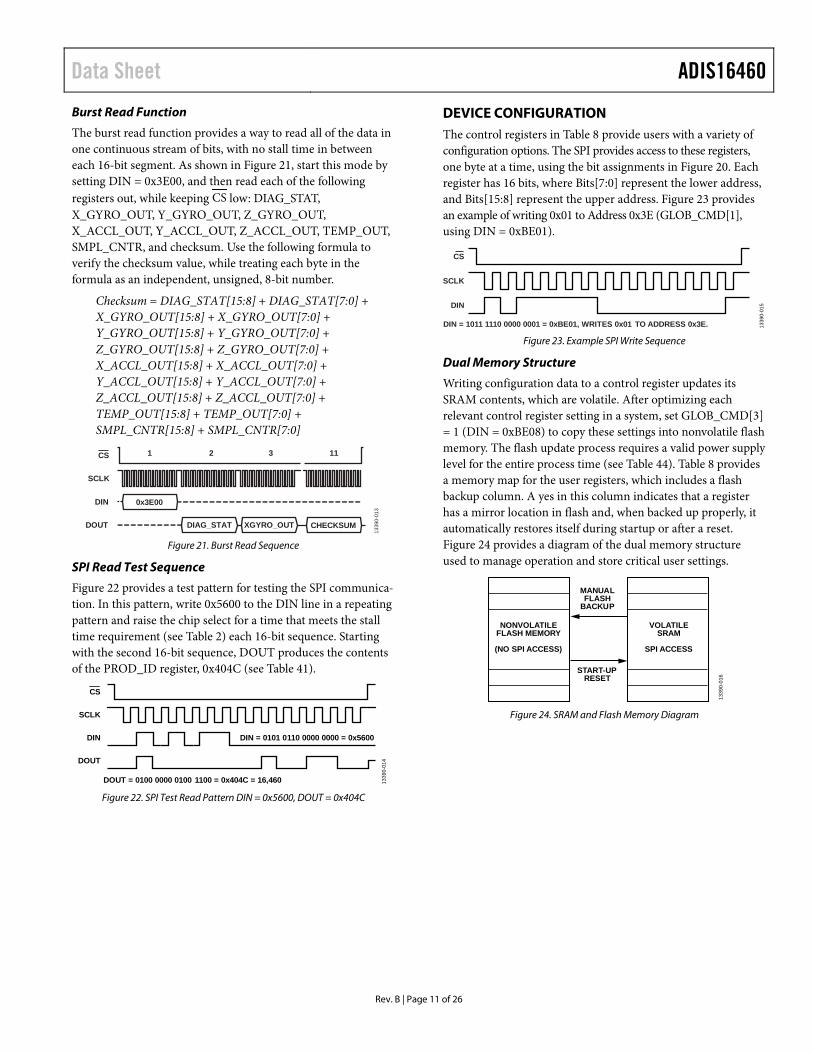
Burst Read Function
The burst read function provides a way to read all of the data in one continuous stream of bits, with no stall time in between each 16-bit segment. As shown in Figure 21, start this mode by setting DIN = 0x3E00, and then read each of the following registers out, while keeping CS low: DIAG_STAT, X_GYRO_OUT, Y_GYRO_OUT, Z_GYRO_OUT, X_ACCL_OUT, Y_ACCL_OUT, Z_ACCL_OUT, TEMP_OUT, SMPL_CNTR, and checksum. Use the following formula to verify the checksum value, while treating each byte in the formula as an independent, unsigned, 8-bit number.
Checksum = DIAG_STAT[15:8] + DIAG_STAT[7:0] + X_GYRO_OUT[15:8] + X_GYRO_OUT[7:0] + Y_GYRO_OUT[15:8] + Y_GYRO_OUT[7:0] + Z_GYRO_OUT[15:8] + Z_GYRO_OUT[7:0] + X_ACCL_OUT[15:8] + X_ACCL_OUT[7:0] + Y_ACCL_OUT[15:8] + Y_ACCL_OUT[7:0] + Z_ACCL_OUT[15:8] + Z_ACCL_OUT[7:0] + TEMP_OUT[15:8] + TEMP_OUT[7:0] + SMPL_CNTR[15:8] + SMPL_CNTR[7:0]
0x3E00
CS
SCLK
DIN
DOUT XGYRO_OUTDIAG_STAT CHECKSUM
1339
0-01
3
1 2 3 11
Figure 21. Burst Read Sequence
SPI Read Test Sequence
Figure 22 provides a test pattern for testing the SPI communica-tion. In this pattern, write 0x5600 to the DIN line in a repeating pattern and raise the chip select for a time that meets the stall time requirement (see Table 2) each 16-bit sequence. Starting with the second 16-bit sequence, DOUT produces the contents of the PROD_ID register, 0x404C (see Table 41).
DOUT = 0100 0000 0100 1100 = 0x404C = 16,460
DIN = 0101 0110 0000 0000 = 0x5600
SCLK
CS
DIN
DOUT
1339
0-01
4
Figure 22. SPI Test Read Pattern DIN = 0x5600, DOUT = 0x404C
DEVICE CONFIGURATION The control registers in Table 8 provide users with a variety of configuration options. The SPI provides access to these registers, one byte at a time, using the bit assignments in Figure 20. Each register has 16 bits, where Bits[7:0] represent the lower address, and Bits[15:8] represent the upper address. Figure 23 provides an example of writing 0x01 to Address 0x3E (GLOB_CMD[1], using DIN = 0xBE01).
SCLK
CS
DIN
DIN = 1011 1110 0000 0001 = 0xBE01, WRITES 0x01 TO ADDRESS 0x3E. 1339
0-01
5
Figure 23. Example SPI Write Sequence
Dual Memory Structure
Writing configuration data to a control register updates its SRAM contents, which are volatile. After optimizing each relevant control register setting in a system, set GLOB_CMD[3] = 1 (DIN = 0xBE08) to copy these settings into nonvolatile flash memory. The flash update process requires a valid power supply level for the entire process time (see Table 44). Table 8 provides a memory map for the user registers, which includes a flash backup column. A yes in this column indicates that a register has a mirror location in flash and, when backed up properly, it automatically restores itself during startup or after a reset. Figure 24 provides a diagram of the dual memory structure used to manage operation and store critical user settings.
NONVOLATILEFLASH MEMORY
(NO SPI ACCESS)
MANUALFLASH
BACKUP
START-UPRESET
VOLATILESRAM
SPI ACCESS
1339
0-01
6
Figure 24. SRAM and Flash Memory Diagram
ADIS16460 Data Sheet
Rev. B | Page 12 of 26
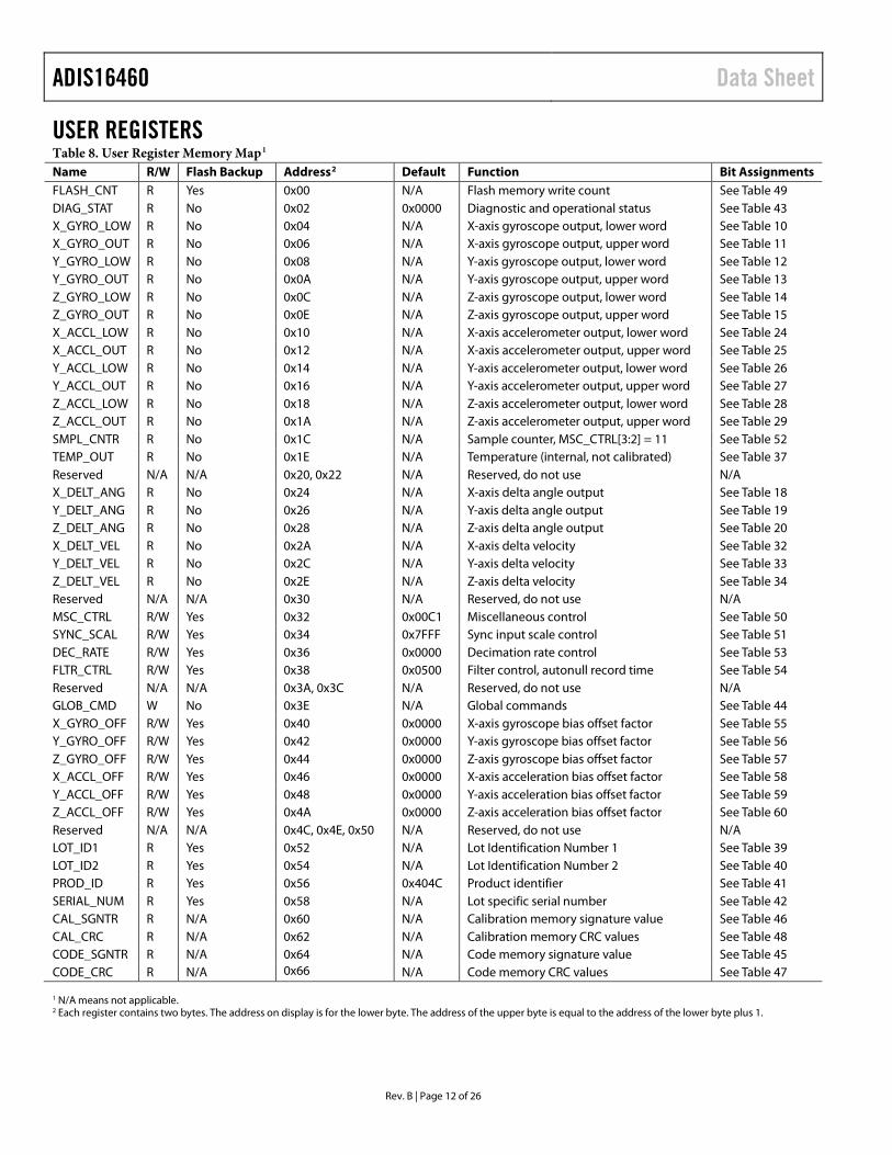
USER REGISTERS Table 8. User Register Memory Map1 Name R/W Flash Backup Address2 Default Function Bit Assignments FLASH_CNT R Yes 0x00 N/A Flash memory write count See Table 49 DIAG_STAT R No 0x02 0x0000 Diagnostic and operational status See Table 43 X_GYRO_LOW R No 0x04 N/A X-axis gyroscope output, lower word See Table 10 X_GYRO_OUT R No 0x06 N/A X-axis gyroscope output, upper word See Table 11 Y_GYRO_LOW R No 0x08 N/A Y-axis gyroscope output, lower word See Table 12 Y_GYRO_OUT R No 0x0A N/A Y-axis gyroscope output, upper word See Table 13 Z_GYRO_LOW R No 0x0C N/A Z-axis gyroscope output, lower word See Table 14 Z_GYRO_OUT R No 0x0E N/A Z-axis gyroscope output, upper word See Table 15 X_ACCL_LOW R No 0x10 N/A X-axis accelerometer output, lower word See Table 24 X_ACCL_OUT R No 0x12 N/A X-axis accelerometer output, upper word See Table 25 Y_ACCL_LOW R No 0x14 N/A Y-axis accelerometer output, lower word See Table 26 Y_ACCL_OUT R No 0x16 N/A Y-axis accelerometer output, upper word See Table 27 Z_ACCL_LOW R No 0x18 N/A Z-axis accelerometer output, lower word See Table 28 Z_ACCL_OUT R No 0x1A N/A Z-axis accelerometer output, upper word See Table 29 SMPL_CNTR R No 0x1C N/A Sample counter, MSC_CTRL[3:2] = 11 See Table 52 TEMP_OUT R No 0x1E N/A Temperature (internal, not calibrated) See Table 37 Reserved N/A N/A 0x20, 0x22 N/A Reserved, do not use N/A X_DELT_ANG R No 0x24 N/A X-axis delta angle output See Table 18 Y_DELT_ANG R No 0x26 N/A Y-axis delta angle output See Table 19 Z_DELT_ANG R No 0x28 N/A Z-axis delta angle output See Table 20 X_DELT_VEL R No 0x2A N/A X-axis delta velocity See Table 32 Y_DELT_VEL R No 0x2C N/A Y-axis delta velocity See Table 33 Z_DELT_VEL R No 0x2E N/A Z-axis delta velocity See Table 34 Reserved N/A N/A 0x30 N/A Reserved, do not use N/A MSC_CTRL R/W Yes 0x32 0x00C1 Miscellaneous control See Table 50 SYNC_SCAL R/W Yes 0x34 0x7FFF Sync input scale control See Table 51 DEC_RATE R/W Yes 0x36 0x0000 Decimation rate control See Table 53 FLTR_CTRL R/W Yes 0x38 0x0500 Filter control, autonull record time See Table 54 Reserved N/A N/A 0x3A, 0x3C N/A Reserved, do not use N/A GLOB_CMD W No 0x3E N/A Global commands See Table 44 X_GYRO_OFF R/W Yes 0x40 0x0000 X-axis gyroscope bias offset factor See Table 55 Y_GYRO_OFF R/W Yes 0x42 0x0000 Y-axis gyroscope bias offset factor See Table 56 Z_GYRO_OFF R/W Yes 0x44 0x0000 Z-axis gyroscope bias offset factor See Table 57 X_ACCL_OFF R/W Yes 0x46 0x0000 X-axis acceleration bias offset factor See Table 58 Y_ACCL_OFF R/W Yes 0x48 0x0000 Y-axis acceleration bias offset factor See Table 59 Z_ACCL_OFF R/W Yes 0x4A 0x0000 Z-axis acceleration bias offset factor See Table 60 Reserved N/A N/A 0x4C, 0x4E, 0x50 N/A Reserved, do not use N/A LOT_ID1 R Yes 0x52 N/A Lot Identification Number 1 See Table 39 LOT_ID2 R Yes 0x54 N/A Lot Identification Number 2 See Table 40 PROD_ID R Yes 0x56 0x404C Product identifier See Table 41 SERIAL_NUM R Yes 0x58 N/A Lot specific serial number See Table 42 CAL_SGNTR R N/A 0x60 N/A Calibration memory signature value See Table 46 CAL_CRC R N/A 0x62 N/A Calibration memory CRC values See Table 48 CODE_SGNTR R N/A 0x64 N/A Code memory signature value See Table 45 CODE_CRC R N/A 0x66 N/A Code memory CRC values See Table 47 1 N/A means not applicable. 2 Each register contains two bytes. The address on display is for the lower byte. The address of the upper byte is equal to the address of the lower byte plus 1.
Data Sheet ADIS16460
Rev. B | Page 13 of 26
OUTPUT DATA REGISTERS The output data registers contain inertial sensor (gyroscopes, accelerometers) measurements, delta angle calculations, delta velocity calculations, and a relative temperature monitor.
ROTATION The ADIS16460 uses iMEMS gyroscopes to provide inertial rotation measurements around three orthogonal axes, in two different formats: angular rate and angular displacement (delta-angles). Figure 26 shows the axial assignments and the direction of rotation that corresponds to a positive response in their respective output registers (see Table 9).
Angular Rate Data
The angular rate of rotation data represents the calibrated response from the tri-axis MEMS gyroscopes. Six registers provide real-time access to these measurements. Each axis has two dedicated registers: a primary and a secondary register. Table 9 provides the register assignments for each of the three axes (ωX, ωY, ωZ) in Figure 26.
Table 9. Angular Rate of Rotation Data Registers Axis Primary Register Secondary Register ωX X_GYRO_OUT (see Table 11) X_GYRO_LOW (see Table 10) ωY Y_GYRO_OUT(see Table 13) Y_GYRO_LOW (see Table 12) ωZ Z_GYRO_OUT (see Table 15) Z_GYRO_LOW (see Table 14)
The primary register provides a 16-bit, twos complement number, where the scale factor (KG) is equal to 0.005°/sec/LSB. The secondary register provides users with the ability to capture the bit growth that is associated with the summation functions in the user configurable digital filters (see Table 53 and Table 54). Figure 25 illustrates how the primary (X_GYRO_OUT) and secondary (X_GYRO_LOW) registers combine to provide a digital result that supports up to 32 bits of digital resolution for the angular rate of rotation around the x-axis.
1339
0-01
8
X-AXIS GYROSCOPE DATA
0 1515 0
X_GYRO_OUT X_GYRO_LOW
Figure 25. 32-Bit Gyroscope Data Format
Table 10. X_GYRO_LOW (Base Address = 0x04), Read Only Bits Description [15:0] X-axis, gyroscope, output data Bit growth from X_GYRO_OUT data path
Table 11. X_GYRO_OUT (Base Address = 0x06), Read Only Bits Description [15:0] X-axis, gyroscope output data, 0.005°/sec/LSB (KG) 0°/sec = 0x0000, twos complement format
Table 12. Y_GYRO_LOW (Base Address = 0x08), Read Only Bits Description [15:0] Y-axis, gyroscope, output data Bit growth from Y_GYRO_OUT data path
Table 13. Y_GYRO_OUT (Base Address = 0x0A), Read Only Bits Description [15:0] Y-axis, gyroscope output data, 0.005°/sec/LSB (KG) 0°/sec = 0x0000, twos complement format
Table 14. Z_GYRO_LOW (Base Address = 0x0C), Read Only Bits Description [15:0] Z-axis, gyroscope, output data Bit growth from Z_GYRO_OUT data path
Table 15. Z_GYRO_OUT (Base Address = 0x0E), Read Only Bits Description [15:0] Z-axis, gyroscope output data, 0.005°/sec/LSB (KG) 0°/sec = 0x0000, twos complement format
1339
0-01
7
Y-AXIS
ωy, Δθy
ωz, Δθz
ωx, Δθx
X-AXIS
Z-AXIS
Figure 26. Inertial Sensor Definitions
ADIS16460 Data Sheet
Rev. B | Page 14 of 26
Table 16 provides seven examples of the digital data format when using only the primary registers for 16-bit measurements.
Table 16. Rotation Rate, 16-Bit Example Rotation Rate (°/sec) Decimal Hex Binary +100 20,000 0x4E20 0100 1110 0010 0000 +0.01 +2 0x0002 0000 0000 0000 0010 +0.005 +1 0x0001 0000 0000 0000 0001 0 0 0x0000 0000 0000 0000 0000 −0.005 −1 0xFFFF 1111 1111 1111 1111 −0.01 −2 0xFFFE 1111 1111 1111 1110 −100 −20,000 0xB1E0 1011 0001 1110 0000
Many, if not all, applications do not require all 32 bits of digital resolution to preserve key sensor performance criteria. When truncating the data width to a lower number of bits, use the follow-ing formula to calculate the scale factor for the least significant bit:
1621LSB1 NGK
where N is the total number of bits.
For example, if the system uses four bits from the x_GYRO_LOW registers, the data width is 20 bits and the LSB weight is equal to 0.0003215°/sec.
162021sec/005.0LSB1
sec/0003125.0161sec/005.0LSB1
Table 17 provides seven examples of the digital data format when using the primary and the secondary registers to produce a 20-bit number for the angular rate of rotation.
Table 17. Rotation Rate, 20-Bit Example Rotation Rate (°/sec) Decimal Hex Binary +100 +320,000 0x4E200 0100 1110 0010 0000 0000 +0.000625 +2 0x00002 0000 0000 0000 0000 0010 +0.0003125 +1 0x00001 0000 0000 0000 0000 0001 0 0 0x00000 0000 0000 0000 0000 0000 −0.0003125 −1 0xFFFFF 1111 1111 1111 1111 1111 −0.000625 −2 0xFFFFE 1111 1111 1111 1111 1110 −100 −320,000 0xB1E00 1011 0001 1110 0000 0000
Delta Angle Data
The delta angle measurements (ΔθX, ΔθY, ΔθX in Figure 26) repre-sent the angular displacement around each axis, during each data processing cycle. Three registers provide real-time access to these measurements, with each axis (x, y, z) having its own dedicated register. X_DELT_ANG (see Table 18) is the output data register for the x-axis (ΔθX in Figure 26), Y_DELT_ANG (see Table 19) is the output data register for the y-axis (ΔθY in Figure 26), and Z_ DELT_ANG (see Table 20) is the output data register for the z-axis (ΔθZ in Figure 26). The scale factors for these registers depend on the scale factor for the gyroscopes (see Table 11, KG = 0.005°/sec/LSB), sample clock (fSAMPLE),
related to MSC_CTRL[3:2] (see Table 50), and the decimation rate settings (DEC_RATE, see Table 53).
Table 18. X_DELT_ANG (Base Address = 0x24), Read Only Bits Description [15:0] X-axis, delta angle output data 0° = 0x0000, twos complement format 1 LSB = KG × (DEC_RATE + 1)/fSAMPLE (degrees) fSAMPLE = 2048 Hz when MSC_CTRL[3:2] = 00 fSAMPLE is the external clock rate when MSC_CTRL[3:2] ≠ 00
Table 19. Y_DELT_ANG (Base Address = 0x26), Read Only Bits Description [15:0] Y-axis, delta angle output data 0° = 0x0000, twos complement format 1 LSB = KG × (DEC_RATE + 1)/fSAMPLE (degrees) fSAMPLE =2048 Hz when MSC_CTRL[3:2] = 00 fSAMPLE is the external clock rate when MSC_CTRL[3:2] ≠ 00
Table 20. Z_DELT_ANG (Base Address = 0x28), Read Only Bits Description [15:0] Z-axis, delta angle output data 0° = 0x0000, twos complement format 1 LSB = KG × (DEC_RATE + 1)/fSAMPLE (degrees) fSAMPLE = 2048 Hz when MSC_CTRL[3:2] = 00 fSAMPLE is the external clock rate when MSC_CTRL[3:2] ≠ 00
Table 21 illustrates the delta angle data format with numerical examples when MSC_CTRL[3:2] = 00 (fSAMPLE = 2048 Hz) and DEC_RATE = 0x0000.
Table 21. x_DELT_ANG Data Format, Example 1 Angle (°)1 Decimal Hex Binary +0.079998 +32,767 0x7FFF 0111 1111 1111 1111 +0.0000048828 +2 0x0002 0000 0000 0000 0010 +0.0000024414 +1 0x0001 0000 0000 0000 0001 0 0 0x0000 0000 0000 0000 0000 −0.0000024414 −1 0xFFFF 1111 1111 1111 1111 −0.0000048828 −2 0xFFFE 1111 1111 1111 1110 −0.080000 −32,768 0x8000 1000 0000 0000 0000 1 MSC_CTRL[3:2] = 00, fSAMPLE = 2048 Hz, and DEC_RATE = 0x0000.
Table 22 illustrates the delta-angle data format with numerical examples when MSC_CTRL[3:2] = 01, the external clock (fSAMPLE) = 2000 Hz and DEC_RATE = 0x0009.
Table 22. x_DELT_ANG Data Format, Example 2 Angle (°)1 Decimal Hex Binary +0.81918 +32,767 0x7FFF 0111 1111 1111 1111 +0.000050 +2 0x0002 0000 0000 0000 0010 +0.000025 +1 0x0001 0000 0000 0000 0001 0 0 0x0000 0000 0000 0000 0000 −0.000025 −1 0xFFFF 1111 1111 1111 1111 −0.000050 −2 0xFFFE 1111 1111 1111 1110 −0.81920 −32,768 0x8000 1000 0000 0000 0000
1 MSC_CTRL[3:2] = 01, fSAMPLE = 2000 Hz, and DEC_RATE = 0x0009.
Data Sheet ADIS16460
Rev. B | Page 15 of 26
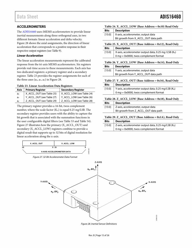
ACCELEROMETERS The ADIS16460 uses iMEMS accelerometers to provide linear inertial measurements along three orthogonal axes, in two different formats: linear acceleration and delta velocity. Figure 28 shows the axial assignments, the direction of linear acceleration that corresponds to a positive response in their respective output registers (see Table 9).
Linear Acceleration
The linear acceleration measurements represent the calibrated response from the tri-axis MEMS accelerometers. Six registers provide real-time access to these measurements. Each axis has two dedicated registers: a primary register and a secondary register. Table 23 provides the register assignments for each of the three axes (aX, aY, aX) in Figure 28.
Table 23. Linear Acceleration Data Registers Axis Primary Register Secondary Register aX X_ACCL_OUT (see Table 25) X_ACCL_LOW (see Table 24) aY Y_ACCL_OUT (see Table 27) Y_ACCL_LOW (see Table 26) aZ Z_ACCL_OUT (see Table 29) Z_ACCL_LOW (see Table 28)
The primary register provides a 16-bit, twos complement number, where the scale factor (KA) is equal 0.25 mg/LSB. The secondary register provides users with the ability to capture the bit growth that is associated with the summation functions in the user configurable digital filters (see Table 53 and Table 54). Figure 27 illustrates how the primary (X_ACCL_OUT) and secondary (X_ACCL_LOW) registers combine to provide a digital result that supports up to 32 bits of digital resolution for linear acceleration along the x-axis.
1339
0-02
0
X-AXIS ACCELEROMETER DATA
0 1515 0
X_ACCL_OUT X_ACCL_LOW
Figure 27. 32-Bit Accelerometer Data Format
Table 24. X_ACCL_LOW (Base Address = 0x10) Read Only Bits Description [15:0] X-axis, accelerometer, output data Bit growth from X_ACCL_OUT data path
Table 25. X_ACCL_OUT (Base Address = 0x12), Read Only Bits Description [15:0] X-axis, accelerometer output data, 0.25 mg /LSB (KA) 0 mg = 0x0000, twos complement format
Table 26. Y_ACCL_LOW (Base Address = 0x14), Read Only Bits Description [15:0] Y-axis, accelerometer, output data Bit growth from Y_ACCL_OUT data path
Table 27. Y_ACCL_OUT (Base Address = 0x16), Read Only Bits Description [15:0] Y-axis, accelerometer output data, 0.25 mg/LSB (KA) 0 mg = 0x0000, twos complement format
Table 28. Z_ACCL_LOW (Base Address = 0x18), Read Only Bits Description [15:0] Z-axis, accelerometer, output data Bit growth from Z_ACCL_OUT data path
Table 29. Z_ACCL_OUT (Base Address = 0x1A), Read Only Bits Description [15:0] Z-axis, accelerometer output data, 0.25 mg/LSB (KA) 0 mg = 0x0000, twos complement format
ay, ΔVy
az, ΔVz
ax, ΔVx
1339
0-01
9
Y-AXIS X-AXIS
Z-AXIS
Figure 28. Inertial Sensor Definitions
ADIS16460 Data Sheet
Rev. B | Page 16 of 26
Table 30 provides seven examples of the digital data format when using only the primary registers for 16-bit measurements.
Table 30. Acceleration, Twos Complement Format Acceleration (mg) Decimal Hex Binary +5000 20,000 0x4E20 0100 1110 0010 0000 +0.5 +2 0x0002 0000 0000 0000 0010 +0.25 +1 0x0001 0000 0000 0000 0001 0 0 0x0000 0000 0000 0000 0000 −0.25 −1 0xFFFF 1111 1111 1111 1111 −0.5 −2 0xFFFE 1111 1111 1111 1110 −5000 −20,000 0xB1E0 1011 0001 1110 0000
Many, if not all, applications do not require all 32 bits of digital resolution to preserve key sensor performance criteria. When truncating the data width to a lower number of bits, use the follow-ing formula to calculate the scale factor for the least significant bit:
1621LSB1 NAK
where N is the total number of bits.
For example, if the system uses two bits from the x_ACCL_LOW registers, the data width is18 bits and the LSB weight is equal to 0.0625 mg.
161821m25.0LSB1 g
gg m0625.041m25.0LSB1
Table 31 provides seven examples of the digital data format when using the primary and secondary registers to produce an 18-bit number for the angular rate of rotation.
Table 31. Acceleration, 18-Bit Example Acceleration (mg) Decimal Hex Binary +5000 80,000 0x13880 01 0011 1000 1000 0000 +0.125 +2 0x00002 00 0000 0000 0000 0010 +0.0625 +1 0x00001 00 0000 0000 0000 0001 0 0 0x00000 00 0000 0000 0000 0000 −0.0625 −1 0x3FFFF 11 1111 1111 1111 1111 −0.125 −2 0x3FFFE 11 1111 1111 1111 1110 −5000 −80,000 0x2C780 10 1100 0111 1000 0000
Delta Velocity Data
The delta velocity measurements (ΔVX, ΔVY, ΔVX in Figure 28) represent the change in velocity along each axis, during each data processing cycle. Three registers provide real-time access to these measurements, with each axis (x, y, z) having its own dedicated register. X_DELT_VEL (see Table 32) is the output data register for the x-axis (ΔVX in Figure 28), Y_ DELT_VEL (see Table 33) is the output data register for the y-axis (ΔVY in Figure 28), and Z_DELT_VEL (see Table 34) is the output data register for the z-axis (ΔVZ in Figure 28). The scale factors for these registers depend on the scale factor for the accelerometers (see Table 25, KA = 0.25 mg/sec/LSB), sample clock (fSAMPLE) related to MSC_CTRL[3:2] (see Table 50), and the decimation rate settings (DEC_RATE, see Table 53).
Table 32. X_DELT_VEL (Base Address = 0x2A), Read Only Bits Description [15:0] X-axis, delta velocity output data 0° = 0x0000, twos complement format 1 LSB = KA × 10 × (DEC_RATE + 1)/fSAMPLE (mm/sec) fSAMPLE = 2048 Hz when MSC_CTRL[3:2] = 00 fSAMPLE is the external clock rate when MSC_CTRL[3:2] ≠ 00
Table 33. Y_DELT_VEL (Base Address = 0x2C), Read Only Bits Description [15:0] Y-axis, delta velocity output data 0° = 0x0000, twos complement format 1 LSB = KA × 10 × (DEC_RATE + 1)/fSAMPLE (mm/sec) fSAMPLE = 2048 Hz when MSC_CTRL[3:2] = 00 fSAMPLE is the external clock rate when MSC_CTRL[3:2] ≠ 00
Table 34. Z_DELT_VEL (Base Address = 0x2E), Read Only Bits Description [15:0] Z-axis, delta velocity output data 0° = 0x0000, twos complement format 1 LSB = KA × 10 × (DEC_RATE + 1)/fSAMPLE (mm/sec) fSAMPLE =2048 Hz when MSC_CTRL[3:2] = 00 fSAMPLE is the external clock rate when MSC_CTRL[3:2] ≠ 00
Table 35 illustrates the delta velocity data format with numerical examples when MSC_CTRL[3:2] = 00, fSAMPLE = 2048 Hz and DEC_RATE = 0x0000.
Table 35. x_DELT_VEL Data Format, Example 1 Velocity (mm/sec)1 Decimal Hex Binary +39.999 +32,767 0x7FFF 0111 1111 1111 1111 +0.0024414 +2 0x0002 0000 0000 0000 0010 +0.0012207 +1 0x0001 0000 0000 0000 0001 0 0 0x0000 0000 0000 0000 0000 −0.0012207 −1 0xFFFF 1111 1111 1111 1111 −0.0024414 −2 0xFFFE 1111 1111 1111 1110 −40 −32,768 0x8000 1000 0000 0000 0000 1 MSC_CTRL[3:2] = 00, fSAMPLE = 2840 Hz, and DEC_RATE = 0x0000.
Data Sheet ADIS16460
Rev. B | Page 17 of 26
Table 36 illustrates the delta velocity data format with numerical examples when MSC_CTRL[3:2] = 01, fSAMPLE is 2000 Hz and DEC_RATE = 0x0009.
Table 36. x_DELT_VEL Data Format, Example 2 Velocity (mm/sec)1 Decimal Hex Binary +409.59 +32,767 0x7FFF 0111 1111 1111 1111 +0.0250 +2 0x0002 0000 0000 0000 0010 +0.0125 +1 0x0001 0000 0000 0000 0001 0 0 0x0000 0000 0000 0000 0000 −0.0125 −1 0xFFFF 1111 1111 1111 1111 −0.0250 −2 0xFFFE 1111 1111 1111 1110 −409.6 −32,768 0x8000 1000 0000 0000 0000 1 MSC_CTRL[3:2] = 01, fSAMPLE = 2000 Hz, and DEC_RATE = 0x0009.
INTERNAL TEMPERATURE The internal temperature measurement data loads into the TEMP_ OUT register (see Table 37). Table 38 illustrates the temperature data format. Note that this temperature represents an internal temperature reading, which does not precisely represent external conditions. The intended use of TEMP_OUT is to monitor relative changes in temperature.
Table 37. TEMP_OUT (Base Address = 0x1E), Read Only Bits Description [15:0] Twos complement, 0.05°C/LSB, 25°C = 0x0000
Table 38. Temperature, Twos Complement Format Temperature (°C) Decimal Hex Binary +105 +1600 0x0640 0000 0110 0100 0000 +85 +1200 0x04B0 0000 0100 1011 0000 +25.1 +2 0x0002 0000 0000 0000 0010 +25.05 +1 0x0001 0000 0000 0000 0001 +25 0 0x0000 0000 0000 0000 0000 +24.95 −1 0xFFFF 1111 1111 1111 1111 +24.90 −2 0xFFFE 1111 1111 1111 1110 −40 −1300 0xFAEC 1111 1010 1110 1100
PRODUCT IDENTIFICATION The PROD_ID register contains the binary equivalent of 16,460 (see Table 41). It provides a product specific variable for systems that need to track this in their system software. The LOT_ID1 and LOT_ID2 registers, respectively, combine to provide a unique, 32-bit lot identification code (see Table 39 and Table 40).
The SERIAL_NUM register contains a binary number that represents the serial number on the device label (see Table 42). The assigned serial numbers in SERIAL_NUM are lot specific.
Table 39. LOT_ID1 (Base Address = 0x52), Read Only Bits Description [15:0] Lot identification, binary code
Table 40. LOT_ID2 (Base Address = 0x54), Read Only Bits Description [15:0] Lot identification, binary code
Table 41. PROD_ID (Base Address = 0x56), Read Only Bits Description (Default = 0x404C) [15:0] Product identification = 0x404C (16,460)
Table 42. SERIAL_NUM (Base Address = 0x58), Read Only Bits Description [15:12] Reserved, values can vary [11:0] Serial number, 1 to 4094 (0xFFE)
STATUS/ERROR FLAGS The DIAG_STAT register in Table 43 contains various bits that serve as error flags for flash update, communication, overrange, self test, and memory integrity. Reading this register provides access to the status of each flag and resets all bits to zero for monitoring future operation. If the error condition remains, the error flag returns to 1 at the conclusion of the next sample cycle.
Table 43. DIAG_STAT (Base Address = 0x02), Read Only Bits Description (Default = 0x0000) [15:8] Not used, always zero [9:8] Reserved, values can vary (not always zero) 7 Input clock out of sync 1 = fail, 0 = pass 6 Flash memory test 1 = fail, 0 = pass 5 Self test diagnostic error flag 1 = fail, 0 = pass 4 Sensor overrange 1 = overrange, 0 = normal 3 SPI communication failure 1 = fail, 0 = pass 2 Flash update failure 1 = fail, 0 = pass [1:0] Not used, always zero
Manual Flash Update
Setting GLOB_CMD[3] = 1 (DIN = 0xBE08, see Table 44) triggers a manual flash update (MFU) routine, which copies the user register settings into manual flash memory, which provides a nonvolatile backup that loads into the registers during the reset or power-on process. After this routine completes, DIAG_STAT[2] contains the pass/fail result. When this bit is set in an error state (equal to 1), trigger another MFU and check DIAG_STAT[2] again after the MFU completes. If this flag remains at zero, it indicates that the latest attempt was completed and that no further action is necessary. Persistence in this error flag can indicate a failure in the flash memory.
ADIS16460 Data Sheet
Rev. B | Page 18 of 26
SPI Communication Failure
This flag (DIAG_STAT[3]) indicates that the total number of SCLK pulses was not equal to an integer multiple of 16, while the chip select (CS) line was low. This flag can be an indication of communication failure; therefore, it can trigger a process of repeating previous commands or a validation of data integrity.
Sensor Overrange
This error flag (DIAG_STAT[4]) indicates that one of the inertial sensors has experienced a condition that exceeds its measurement range.
Self Test Failure
The DIAG_STAT[5] bit provides the result from the automated self test function, which is associated with GLOB_CMD[2] (see Table 44). When this bit is set in an error state (equal to 1), trigger
another automated self test (AST) and check DIAG_STAT[5] again after the AST completes. If this flag remains at zero, it indicates that the latest attempt was completed and that no further action is necessary. Persistence in this error flag can indicate a failure in one or more of the inertial sensors.
Flash Test Failure
DIAG_STAT[6] (see Table 43) contains the result of the memory test, which executes after setting GLOB_CMD[4] = 1 (DIN = 0xBE10, see Table 44).
Input Clock Sync Failure
This error flag (DIAG_STAT[7] = 1) indicates that the SYNC_ SCAL value is not appropriate for the frequency of the signal on the SYNC pin.
Data Sheet ADIS16460
Rev. B | Page 19 of 26
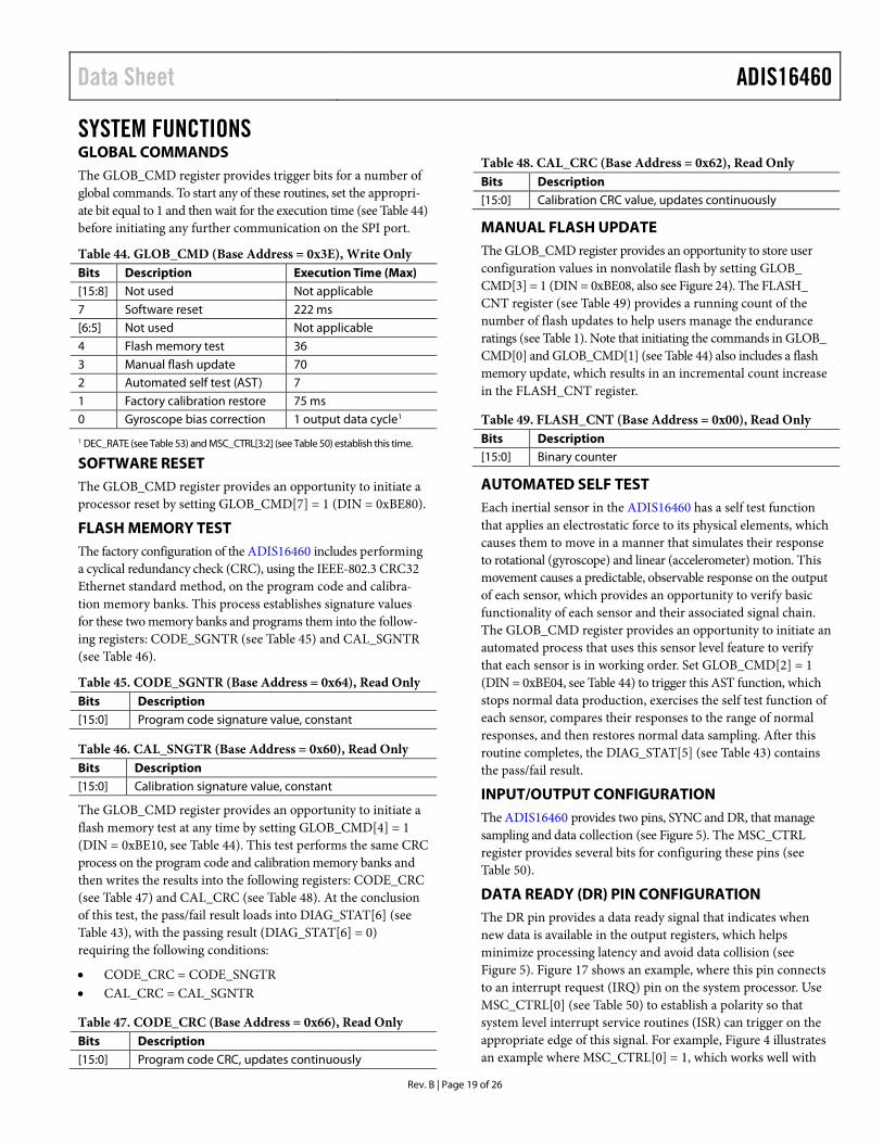
SYSTEM FUNCTIONS GLOBAL COMMANDS The GLOB_CMD register provides trigger bits for a number of global commands. To start any of these routines, set the appropri-ate bit equal to 1 and then wait for the execution time (see Table 44) before initiating any further communication on the SPI port.
Table 44. GLOB_CMD (Base Address = 0x3E), Write Only Bits Description Execution Time (Max) [15:8] Not used Not applicable 7 Software reset 222 ms [6:5] Not used Not applicable 4 Flash memory test 36 3 Manual flash update 70 2 Automated self test (AST) 7 1 Factory calibration restore 75 ms 0 Gyroscope bias correction 1 output data cycle1
1 DEC_RATE (see Table 53) and MSC_CTRL[3:2] (see Table 50) establish this time.
SOFTWARE RESET The GLOB_CMD register provides an opportunity to initiate a processor reset by setting GLOB_CMD[7] = 1 (DIN = 0xBE80).
FLASH MEMORY TEST The factory configuration of the ADIS16460 includes performing a cyclical redundancy check (CRC), using the IEEE-802.3 CRC32 Ethernet standard method, on the program code and calibra-tion memory banks. This process establishes signature values for these two memory banks and programs them into the follow-ing registers: CODE_SGNTR (see Table 45) and CAL_SGNTR (see Table 46).
Table 45. CODE_SGNTR (Base Address = 0x64), Read Only Bits Description [15:0] Program code signature value, constant
Table 46. CAL_SNGTR (Base Address = 0x60), Read Only Bits Description [15:0] Calibration signature value, constant
The GLOB_CMD register provides an opportunity to initiate a flash memory test at any time by setting GLOB_CMD[4] = 1 (DIN = 0xBE10, see Table 44). This test performs the same CRC process on the program code and calibration memory banks and then writes the results into the following registers: CODE_CRC (see Table 47) and CAL_CRC (see Table 48). At the conclusion of this test, the pass/fail result loads into DIAG_STAT[6] (see Table 43), with the passing result (DIAG_STAT[6] = 0) requiring the following conditions:
• CODE_CRC = CODE_SNGTR • CAL_CRC = CAL_SGNTR
Table 47. CODE_CRC (Base Address = 0x66), Read Only Bits Description [15:0] Program code CRC, updates continuously
Table 48. CAL_CRC (Base Address = 0x62), Read Only Bits Description [15:0] Calibration CRC value, updates continuously
MANUAL FLASH UPDATE The GLOB_CMD register provides an opportunity to store user configuration values in nonvolatile flash by setting GLOB_ CMD[3] = 1 (DIN = 0xBE08, also see Figure 24). The FLASH_ CNT register (see Table 49) provides a running count of the number of flash updates to help users manage the endurance ratings (see Table 1). Note that initiating the commands in GLOB_ CMD[0] and GLOB_CMD[1] (see Table 44) also includes a flash memory update, which results in an incremental count increase in the FLASH_CNT register.
Table 49. FLASH_CNT (Base Address = 0x00), Read Only Bits Description [15:0] Binary counter
AUTOMATED SELF TEST Each inertial sensor in the ADIS16460 has a self test function that applies an electrostatic force to its physical elements, which causes them to move in a manner that simulates their response to rotational (gyroscope) and linear (accelerometer) motion. This movement causes a predictable, observable response on the output of each sensor, which provides an opportunity to verify basic functionality of each sensor and their associated signal chain. The GLOB_CMD register provides an opportunity to initiate an automated process that uses this sensor level feature to verify that each sensor is in working order. Set GLOB_CMD[2] = 1 (DIN = 0xBE04, see Table 44) to trigger this AST function, which stops normal data production, exercises the self test function of each sensor, compares their responses to the range of normal responses, and then restores normal data sampling. After this routine completes, the DIAG_STAT[5] (see Table 43) contains the pass/fail result.
INPUT/OUTPUT CONFIGURATION The ADIS16460 provides two pins, SYNC and DR, that manage sampling and data collection (see Figure 5). The MSC_CTRL register provides several bits for configuring these pins (see Table 50).
DATA READY (DR) PIN CONFIGURATION The DR pin provides a data ready signal that indicates when new data is available in the output registers, which helps minimize processing latency and avoid data collision (see Figure 5). Figure 17 shows an example, where this pin connects to an interrupt request (IRQ) pin on the system processor. Use MSC_CTRL[0] (see Table 50) to establish a polarity so that system level interrupt service routines (ISR) can trigger on the appropriate edge of this signal. For example, Figure 4 illustrates an example where MSC_CTRL[0] = 1, which works well with
ADIS16460 Data Sheet
Rev. B | Page 20 of 26
IRQ pins that trigger on the positive edge of a pulse. When DR is driving an IRQ pin that triggers on the negative edge of a signal, set DIN = 0xB2C3 (MSC_CTRL[7:0] = 0xC3). This code also preserves the factory default configuration for the linear g compensation (MSC_CTRL[7]) and point of percussion (MSC_ CTRL[6]). Note that the data ready signal stops while the device executes the global commands associated with the GLOB_CMD register (see Table 44).
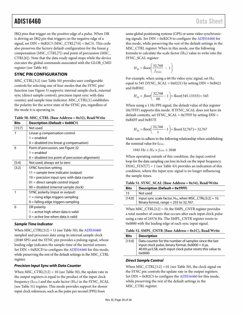
SYNC PIN CONFIGURATION MSC_CTRL[3:2] (see Table 50) provides user configurable controls for selecting one of four modes that the SYNC pin/ function (see Figure 5) supports: internal sample clock, external sync (direct sample control), precision input sync with data counter, and sample time indicator. MSC_CTRL[1] establishes the polarity for the active state of the SYNC pin, regardless of the mode it is operating in.
Table 50. MSC_CTRL (Base Address = 0x32), Read/Write Bits Description (Default = 0x00C1) [15:7] Not used 7 Linear-g compensation control 1 = enabled 0 = disabled (no linear-g compensation) 6 Point of percussion, see Figure 32 1 = enabled 0 = disabled (no point of percussion alignment) [5:4] Not used, always set to zero [3:2] SYNC function setting 11 = sample time indicator (output) 10 = precision input sync with data counter 01 = direct sample control (input) 00 = disabled (internal sample clock) 1 SYNC polarity (input or output) 1 = rising edge triggers sampling 0 = falling edge triggers sampling 0 DR polarity 1 = active high when data is valid 0 = active low when data is valid
Sample Time Indicator
When MSC_CTRL[3:2] = 11 (see Table 50), the ADIS16460 sampled and processes data using its internal sample clock (2048 SPS) and the SYNC pin provides a pulsing signal, whose leading edge indicates the sample time of the inertial sensors. Set DIN = 0xB2CD to configure the ADIS16460 for this mode, while preserving the rest of the default settings in the MSC_CTRL register.
Precision Input Sync with Data Counter
When MSC_CTRL[3:2] = 10 (see Table 50), the update rate in the output registers is equal to the product of the input clock frequency (fSYNC) and the scale factor (HSS) in the SYNC_SCAL (see Table 51) register. This mode provides support for slower input clock references, such as the pulse per second (PPS) from
some global positioning systems (GPS) or some video synchroniz-ing signals. Set DIN = 0xB2C9 to configure the ADIS16460 for this mode, while preserving the rest of the default settings in the MSC_CTRL register. When in this mode, use the following formula to calculate the scale factor (HSS) value to write into the SYNC_SCAL register:
−= 1768,32floor
SYNCSS f
H
For example, when using a 60 Hz video sync signal, set HSS equal to 545 (SYNC_SCAL = 0x0221) by setting DIN = 0xB421 and 0xB502.
( ) 54513333.545floor160768,32
==
−= floorHSS
When using a 1 Hz PPS signal, the default value of this register (0x7FFF) supports this mode. If SYNC_SCAL does not have its default contents, set SYNC_SCAL = 0x7FFF by setting DIN = 0xB4FF and 0xB57F.
( ) 767,32767,32floor11
32,768floor ==
−=SSH
Make sure to adhere to the following relationship when establishing the nominal value for fSYNC.
1945 Hz ≤ HSS × fSYNC ≤ 2048
When operating outside of this condition, the input control loop for the data sampling can lose its lock on the input frequency. DIAG_STAT[7] = 1 (see Table 43) provides an indication of this condition, where the input sync signal is no longer influencing the sample times.
Table 51. SYNC_SCAL (Base Address = 0x34), Read/Write Bits Description (Default = 0x7FFF) 15 Not used [14:0] Input sync scale factor, HSS, when MSC_CTRL[3:2] = 10.
Binary format, range = 255 to 32,767.
When MSC_CTRL[3:2] = 10, the SMPL_CNTR register provides a total number of counts that occurs after each input clock pulse using a rate of 24576 Hz. The SMPL_CNTR register resets to 0x0000 with the leading edge of each sync input signal.
Table 52. SMPL_CNTR (Base Address = 0x1C), Read/Write Bits Description [15:0] Data counter for the number of samples since the last
input clock pulse, binary format, 0x0000 = 0 μs, 40.69 μs/LSB, each input clock pulse resets this value to 0x0000
Direct Sample Control
When MSC_CTRL[3:2] = 01 (see Table 50), the clock signal on the SYNC pin controls the update rate in the output registers. Set DIN = 0xB2C5 to configure the ADIS16460 for this mode, while preserving the rest of the default settings in the MSC_CTRL register.
Data Sheet ADIS16460
Rev. B | Page 21 of 26
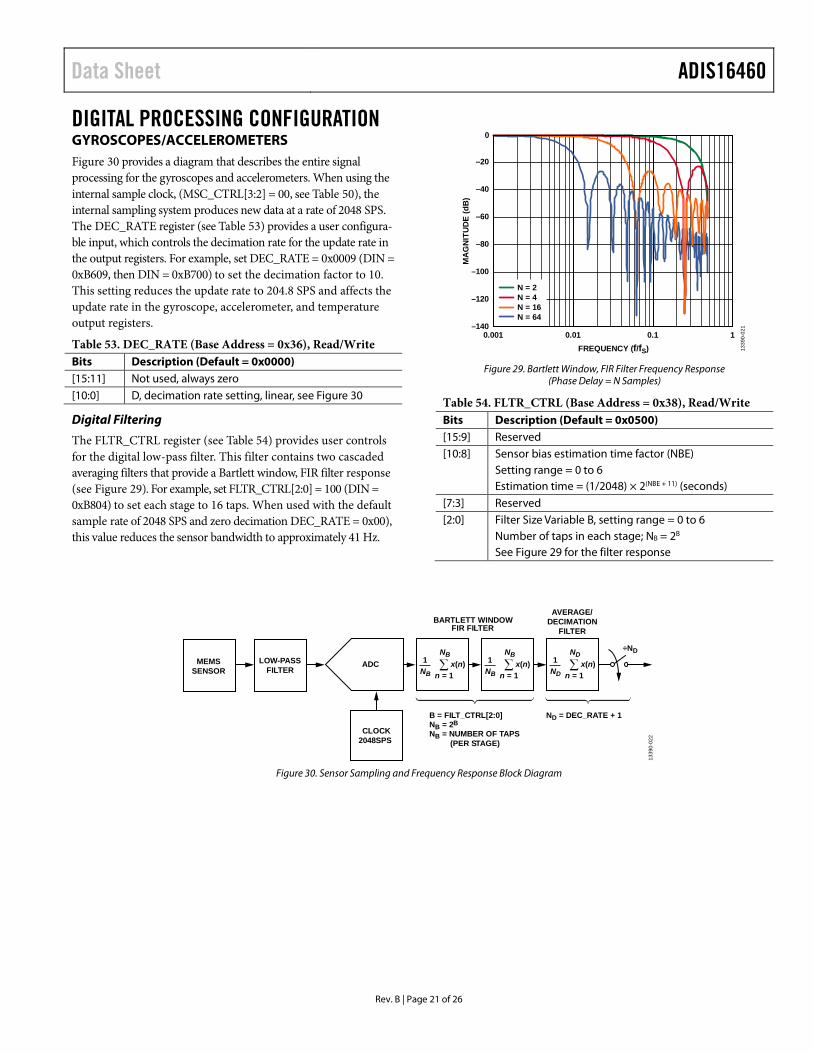
DIGITAL PROCESSING CONFIGURATION GYROSCOPES/ACCELEROMETERS Figure 30 provides a diagram that describes the entire signal processing for the gyroscopes and accelerometers. When using the internal sample clock, (MSC_CTRL[3:2] = 00, see Table 50), the internal sampling system produces new data at a rate of 2048 SPS. The DEC_RATE register (see Table 53) provides a user configura-ble input, which controls the decimation rate for the update rate in the output registers. For example, set DEC_RATE = 0x0009 (DIN = 0xB609, then DIN = 0xB700) to set the decimation factor to 10. This setting reduces the update rate to 204.8 SPS and affects the update rate in the gyroscope, accelerometer, and temperature output registers.
Table 53. DEC_RATE (Base Address = 0x36), Read/Write Bits Description (Default = 0x0000) [15:11] Not used, always zero [10:0] D, decimation rate setting, linear, see Figure 30
Digital Filtering
The FLTR_CTRL register (see Table 54) provides user controls for the digital low-pass filter. This filter contains two cascaded averaging filters that provide a Bartlett window, FIR filter response (see Figure 29). For example, set FLTR_CTRL[2:0] = 100 (DIN = 0xB804) to set each stage to 16 taps. When used with the default sample rate of 2048 SPS and zero decimation DEC_RATE = 0x00), this value reduces the sensor bandwidth to approximately 41 Hz.
0
–20
–40
–60
–80
–100
–120
–1400.001 0.01 0.1 1
MA
GN
ITU
DE
(dB
)
FREQUENCY (f/fS)
N = 2N = 4N = 16N = 64
1339
0-02
1
Figure 29. Bartlett Window, FIR Filter Frequency Response
(Phase Delay = N Samples)
Table 54. FLTR_CTRL (Base Address = 0x38), Read/Write Bits Description (Default = 0x0500) [15:9] Reserved [10:8] Sensor bias estimation time factor (NBE) Setting range = 0 to 6 Estimation time = (1/2048) × 2(NBE + 11) (seconds) [7:3] Reserved [2:0] Filter Size Variable B, setting range = 0 to 6 Number of taps in each stage; NB = 2B See Figure 29 for the filter response
MEMSSENSOR
LOW-PASSFILTER
CLOCK2048SPS
ADC
BARTLETT WINDOWFIR FILTER
AVERAGE/DECIMATION
FILTER
B = FILT_CTRL[2:0]NB = 2BNB = NUMBER OF TAPS (PER STAGE)
ND = DEC_RATE + 1
÷ND
x(n)n = 1
1NB
NBx(n)
n = 1
1NB
NBx(n)
n = 1
1ND
ND
1339
0-02
2
Figure 30. Sensor Sampling and Frequency Response Block Diagram
ADIS16460 Data Sheet
Rev. B | Page 22 of 26
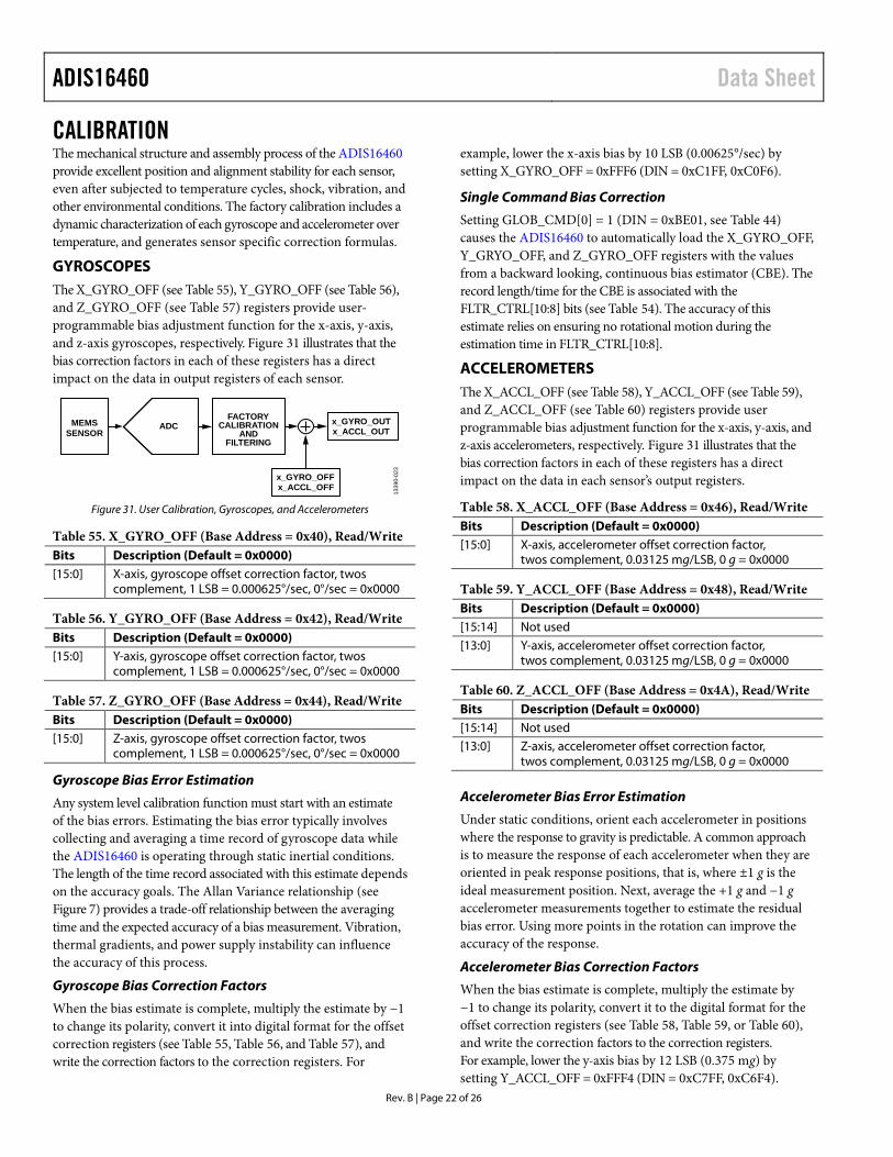
CALIBRATION The mechanical structure and assembly process of the ADIS16460 provide excellent position and alignment stability for each sensor, even after subjected to temperature cycles, shock, vibration, and other environmental conditions. The factory calibration includes a dynamic characterization of each gyroscope and accelerometer over temperature, and generates sensor specific correction formulas.
GYROSCOPES The X_GYRO_OFF (see Table 55), Y_GYRO_OFF (see Table 56), and Z_GYRO_OFF (see Table 57) registers provide user-programmable bias adjustment function for the x-axis, y-axis, and z-axis gyroscopes, respectively. Figure 31 illustrates that the bias correction factors in each of these registers has a direct impact on the data in output registers of each sensor.
x_GYRO_OFFx_ACCL_OFF
MEMSSENSOR
ADCFACTORY
CALIBRATIONAND
FILTERING
x_GYRO_OUTx_ACCL_OUT
1339
0-02
3
Figure 31. User Calibration, Gyroscopes, and Accelerometers
Table 55. X_GYRO_OFF (Base Address = 0x40), Read/Write Bits Description (Default = 0x0000) [15:0] X-axis, gyroscope offset correction factor, twos
complement, 1 LSB = 0.000625°/sec, 0°/sec = 0x0000
Table 56. Y_GYRO_OFF (Base Address = 0x42), Read/Write Bits Description (Default = 0x0000) [15:0] Y-axis, gyroscope offset correction factor, twos
complement, 1 LSB = 0.000625°/sec, 0°/sec = 0x0000
Table 57. Z_GYRO_OFF (Base Address = 0x44), Read/Write Bits Description (Default = 0x0000) [15:0] Z-axis, gyroscope offset correction factor, twos
complement, 1 LSB = 0.000625°/sec, 0°/sec = 0x0000
Gyroscope Bias Error Estimation
Any system level calibration function must start with an estimate of the bias errors. Estimating the bias error typically involves collecting and averaging a time record of gyroscope data while the ADIS16460 is operating through static inertial conditions. The length of the time record associated with this estimate depends on the accuracy goals. The Allan Variance relationship (see Figure 7) provides a trade-off relationship between the averaging time and the expected accuracy of a bias measurement. Vibration, thermal gradients, and power supply instability can influence the accuracy of this process.
Gyroscope Bias Correction Factors
When the bias estimate is complete, multiply the estimate by −1 to change its polarity, convert it into digital format for the offset correction registers (see Table 55, Table 56, and Table 57), and write the correction factors to the correction registers. For
example, lower the x-axis bias by 10 LSB (0.00625°/sec) by setting X_GYRO_OFF = 0xFFF6 (DIN = 0xC1FF, 0xC0F6).
Single Command Bias Correction
Setting GLOB_CMD[0] = 1 (DIN = 0xBE01, see Table 44) causes the ADIS16460 to automatically load the X_GYRO_OFF, Y_GRYO_OFF, and Z_GYRO_OFF registers with the values from a backward looking, continuous bias estimator (CBE). The record length/time for the CBE is associated with the FLTR_CTRL[10:8] bits (see Table 54). The accuracy of this estimate relies on ensuring no rotational motion during the estimation time in FLTR_CTRL[10:8].
ACCELEROMETERS The X_ACCL_OFF (see Table 58), Y_ACCL_OFF (see Table 59), and Z_ACCL_OFF (see Table 60) registers provide user programmable bias adjustment function for the x-axis, y-axis, and z-axis accelerometers, respectively. Figure 31 illustrates that the bias correction factors in each of these registers has a direct impact on the data in each sensor’s output registers.
Table 58. X_ACCL_OFF (Base Address = 0x46), Read/Write Bits Description (Default = 0x0000) [15:0] X-axis, accelerometer offset correction factor,
twos complement, 0.03125 mg/LSB, 0 g = 0x0000
Table 59. Y_ACCL_OFF (Base Address = 0x48), Read/Write Bits Description (Default = 0x0000) [15:14] Not used [13:0] Y-axis, accelerometer offset correction factor,
twos complement, 0.03125 mg/LSB, 0 g = 0x0000
Table 60. Z_ACCL_OFF (Base Address = 0x4A), Read/Write Bits Description (Default = 0x0000) [15:14] Not used [13:0] Z-axis, accelerometer offset correction factor,
twos complement, 0.03125 mg/LSB, 0 g = 0x0000
Accelerometer Bias Error Estimation
Under static conditions, orient each accelerometer in positions where the response to gravity is predictable. A common approach is to measure the response of each accelerometer when they are oriented in peak response positions, that is, where ±1 g is the ideal measurement position. Next, average the +1 g and −1 g accelerometer measurements together to estimate the residual bias error. Using more points in the rotation can improve the accuracy of the response.
Accelerometer Bias Correction Factors
When the bias estimate is complete, multiply the estimate by −1 to change its polarity, convert it to the digital format for the offset correction registers (see Table 58, Table 59, or Table 60), and write the correction factors to the correction registers. For example, lower the y-axis bias by 12 LSB (0.375 mg) by setting Y_ACCL_OFF = 0xFFF4 (DIN = 0xC7FF, 0xC6F4).
Data Sheet ADIS16460
Rev. B | Page 23 of 26
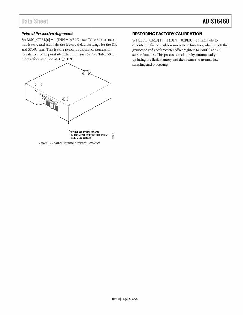
Point of Percussion Alignment
Set MSC_CTRL[6] = 1 (DIN = 0xB2C1, see Table 50) to enable this feature and maintain the factory default settings for the DR and SYNC pins. This feature performs a point of percussion translation to the point identified in Figure 32. See Table 50 for more information on MSC_CTRL.
POINT OF PERCUSSIONALIGNMENT REFERENCE POINTSEE MSC_CTRL[6] 13
390-
024
Figure 32. Point of Percussion Physical Reference
RESTORING FACTORY CALIBRATION Set GLOB_CMD[1] = 1 (DIN = 0xBE02, see Table 44) to execute the factory calibration restore function, which resets the gyroscope and accelerometer offset registers to 0x0000 and all sensor data to 0. This process concludes by automatically updating the flash memory and then returns to normal data sampling and processing.
ADIS16460 Data Sheet
Rev. B | Page 24 of 26
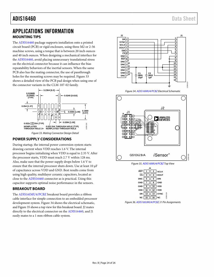
APPLICATIONS INFORMATION MOUNTING TIPS The ADIS16460 package supports installation onto a printed circuit board (PCB) or rigid enclosure, using three M2 or 2-56 machine screws, using a torque that is between 20 inch ounces and 40 inch ounces. When designing a mechanical interface for the ADIS16460, avoid placing unnecessary translational stress on the electrical connector because it can influence the bias repeatability behaviors of the inertial sensors. When the same PCB also has the mating connector, the use of passthrough holes for the mounting screws may be required. Figure 33 shows a detailed view of the PCB pad design when using one of the connector variants in the CLM-107-02 family.
0.2364 [6.0]
0.0240 [0.610]0.019685[0.5000]
(TYP)
0.054 [1.37]
0.0394 [1.00]
0.0394 [1.00] 0.1800[4.57]
NONPLATEDTHROUGH HOLE 2×
0.022± DIA (TYP)0.0030.000
0.022 DIA THROUGH HOLE (TYP)NONPLATED THROUGH HOLE 13
390-
026
Figure 33. Mating Connector Design Detail
POWER SUPPLY CONSIDERATIONS During startup, the internal power conversion system starts drawing current when VDD reaches 1.6 V. The internal processor begins initializing when VDD is equal to 2.35 V. After the processor starts, VDD must reach 2.7 V within 128 ms. Also, make sure that the power supply drops below 1.6 V to ensure that the internal processor shuts down. Use at least 10 µF of capacitance across VDD and GND. Best results come from using high quality, multilayer ceramic capacitors, located as close to the ADIS16460 connector as is practical. Using this capacitor supports optimal noise performance in the sensors.
BREAKOUT BOARD The ADIS16IMU4/PCBZ breakout board provides a ribbon cable interface for simple connection to an embedded processor development system. Figure 34 shows the electrical schematic, and Figure 35 shows a top view for this breakout board. J2 mates directly to the electrical connector on the ADIS16460, and J1 easily mates to a 1 mm ribbon cable system.
1339
0-02
7
C1080510µF
C206031µF
123456789
10111213141516
J2 J11234567891011121314
DRSYNCSCLKDOUT
DINCS
DNCRSTDNCDNCVDDDNCGNDDNC
Figure 34. ADIS16IMU4/PCBZ Electrical Schematic
1339
0-02
8
Figure 35. ADIS16IMU4/PCBZ Top View 13
390-
029
1RST 2J1
3CS 4 DOUTSCLK
5DNC 6 DIN
7GND 8 GND
9GND 10 VDD
11VDD 12 VDD
13DR 14 SYNC
15NC 16 NC
Figure 36. ADIS16IUMU4/PCBZ J1 Pin Assignments

Data Sheet ADIS16460
Rev. B | Page 25 of 26
PC-BASED EVALUATION TOOLS The ADIS16IMU4/PCBZ provides a simple way to connect the ADIS16460 to the EVAL-ADIS evaluation system, which provides a PC-based method for evaluation of basic function and performance. For more information, visit the following wiki guide: ADIS1646X/AD24000 Evaluation on a PC.
Estimating the Number of Relevant Bits
The primary output data registers provide 16 bits of resolution for each of the inertial sensors, which is sufficient for preserving key sensor behaviors when the internal filters are not in use and when collecting every sample that the ADIS16460 loads into its output registers. For systems that use the internal filtering, the secondary output data registers capture the bit growth that comes from the accumulation functions in these filters. The magnitude of this bit growth depends on the settings in both of these registers. Use the variable settings (D in Table 53, B in Table 54) and the following formula to calculate the total number of summation functions (NS), along with the associated bit growth in the data path (NBG):
NS = D + 2B
NBG = √NS
For example, if B = 5 and D = 4, the bit growth in the internal data path is six bits, which means that only the upper six bits of each secondary register (X_GYRO_LOW[15:10], for example) have relevance.
NS = D + 2B = 4 + 25 = 36 samples
NBG = √NS = √36 = 6 bits
The stability performance of each sensor is worth consideration as well, when determining the number of bits to carry through-out the data path in a system processor. For example, preserving the six most significant bits in the secondary registers for the gyroscopes provides a digital resolution of 0.000078125°/sec, or ~0.28°/hour, which is significantly lower than the in-run bias stability of the ADIS16460 gyroscopes.
ADIS16460 Data Sheet
Rev. B | Page 26 of 26
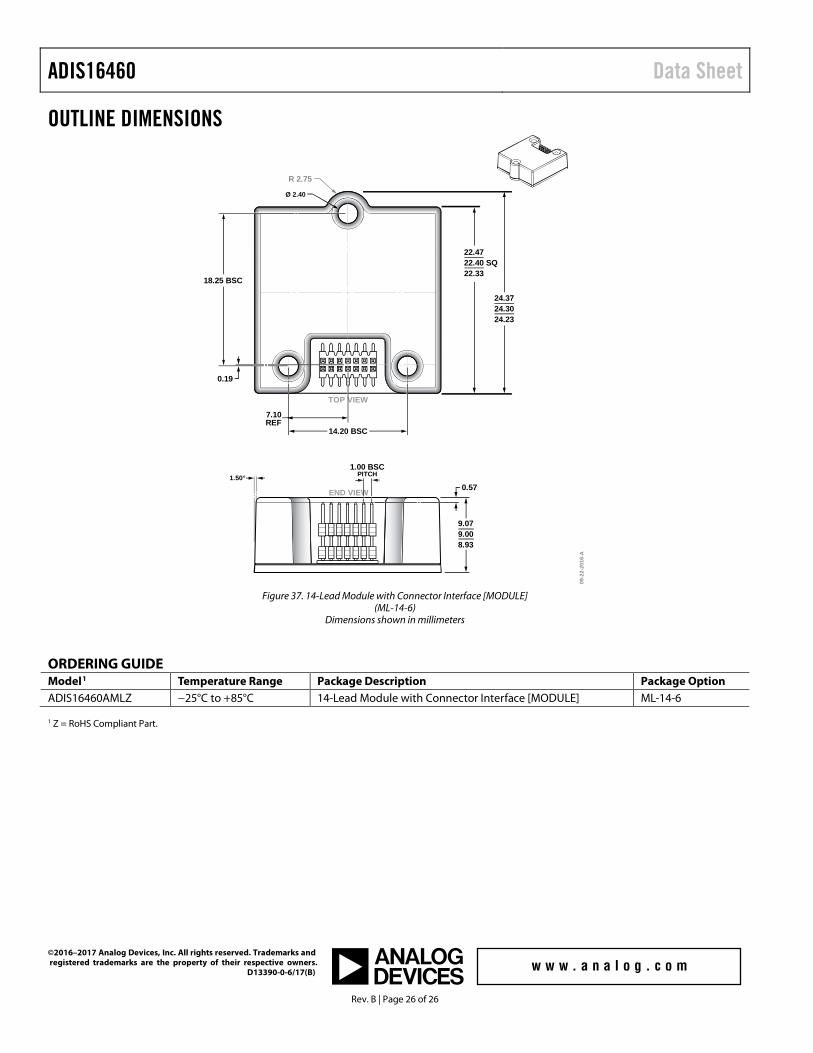
OUTLINE DIMENSIONS
09-2
2-20
16-A
TOP VIEW
END VIEW
22.4722.40 SQ22.33
24.3724.3024.23
9.079.008.93
18.25 BSC
14.20 BSC
1.00 BSCPITCH
7.10REF
0.19
0.57
R 2.75
Ø 2.40
1.50°
Figure 37. 14-Lead Module with Connector Interface [MODULE]
(ML-14-6) Dimensions shown in millimeters
ORDERING GUIDE Model1 Temperature Range Package Description Package Option ADIS16460AMLZ −25°C to +85°C 14-Lead Module with Connector Interface [MODULE] ML-14-6 1 Z = RoHS Compliant Part.
©2016–2017 Analog Devices, Inc. All rights reserved. Trademarks and registered trademarks are the property of their respective owners. D13390-0-6/17(B)