T f i Li ht ith M t t i l Transforming Light with...
21
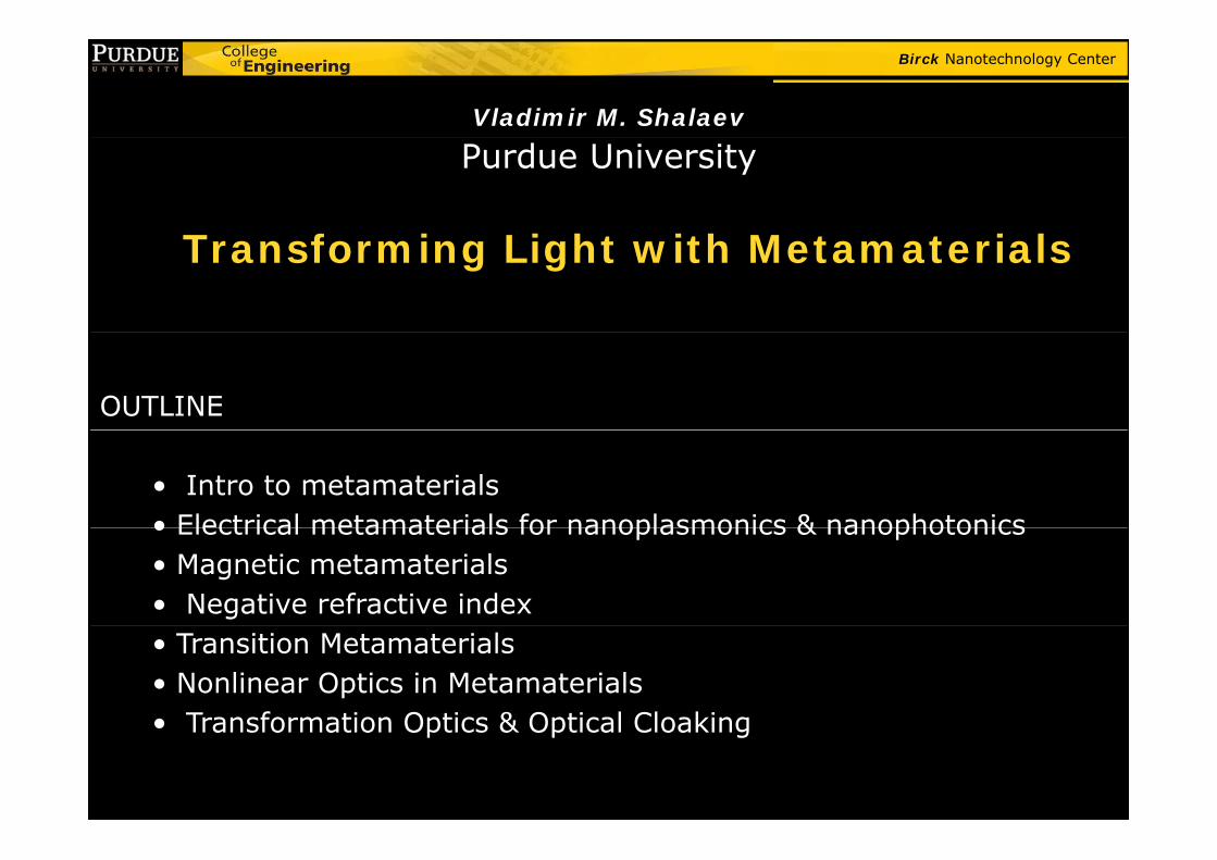
Birck Nanotechnology Center Birck Nanotechnology Center Vladimir M. Shalaev T f i Li ht ith M t t il Purdue University Transforming Light with Metamaterials OUTLINE • Intro to metamaterials • Electrical metamaterials for nanoplasmonics & nanophotonics • Electrical metamaterials for nanoplasmonics & nanophotonics • Magnetic metamaterials • Negative refractive index • Transition Metamaterials • Nonlinear Optics in Metamaterials • Transformation Optics & Optical Cloaking • Transformation Optics & Optical Cloaking
-
Upload
nguyenliem -
Category
Documents
-
view
216 -
download
2
Transcript of T f i Li ht ith M t t i l Transforming Light with...
Birck Nanotechnology CenterBirck Nanotechnology Center
Vladimir M. Shalaev
T f i Li ht ith M t t i l
Purdue University
Transforming Light with Metamaterials
OUTLINE
• Intro to metamaterials• Electrical metamaterials for nanoplasmonics & nanophotonics• Electrical metamaterials for nanoplasmonics & nanophotonics• Magnetic metamaterials• Negative refractive index• Transition Metamaterials• Nonlinear Optics in Metamaterials• Transformation Optics & Optical Cloaking • Transformation Optics & Optical Cloaking
Birck Nanotechnology Center
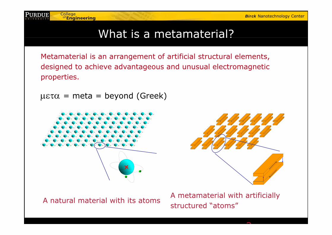
What is a metamaterial?What is a metamaterial?
Metamaterial is an arrangement of artificial structural elements, d i d t hi d t d l l t ti designed to achieve advantageous and unusual electromagnetic properties.
= meta = beyond (Greek)
--
A metamaterial with artificially
2
A natural material with its atomsA metamaterial with artificially structured “atoms”
Birck Nanotechnology Center
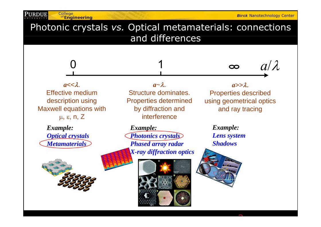
Photonic crystals vs. Optical metamaterials: connections d diffand differences
a<< . a~ a>>Effective mediumdescription using
Maxwell equations with
Structure dominates.Properties determined
by diffraction and
Properties describedusing geometrical optics
and ray tracing, , n, Z interference
Example:Optical crystals
Example:Photonics crystals
Example:Lens systemp y
Metamaterialsy
Phased array radarX-ray diffraction optics
Shadows
3
Birck Nanotechnology Center
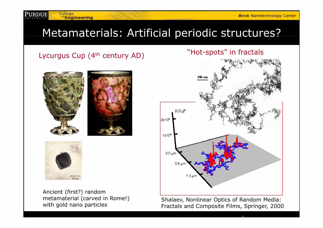
Metamaterials: Artificial periodic structures?Metamaterials: Artificial periodic structures?
“Hot-spots” in fractalsLycurgus Cup (4th century AD)
Ancient (first?) random
4
Shalaev, Nonlinear Optics of Random Media: Fractals and Composite Films, Springer, 2000
Ancient (first?) random metamaterial (carved in Rome!) with gold nano particles
Birck Nanotechnology Center
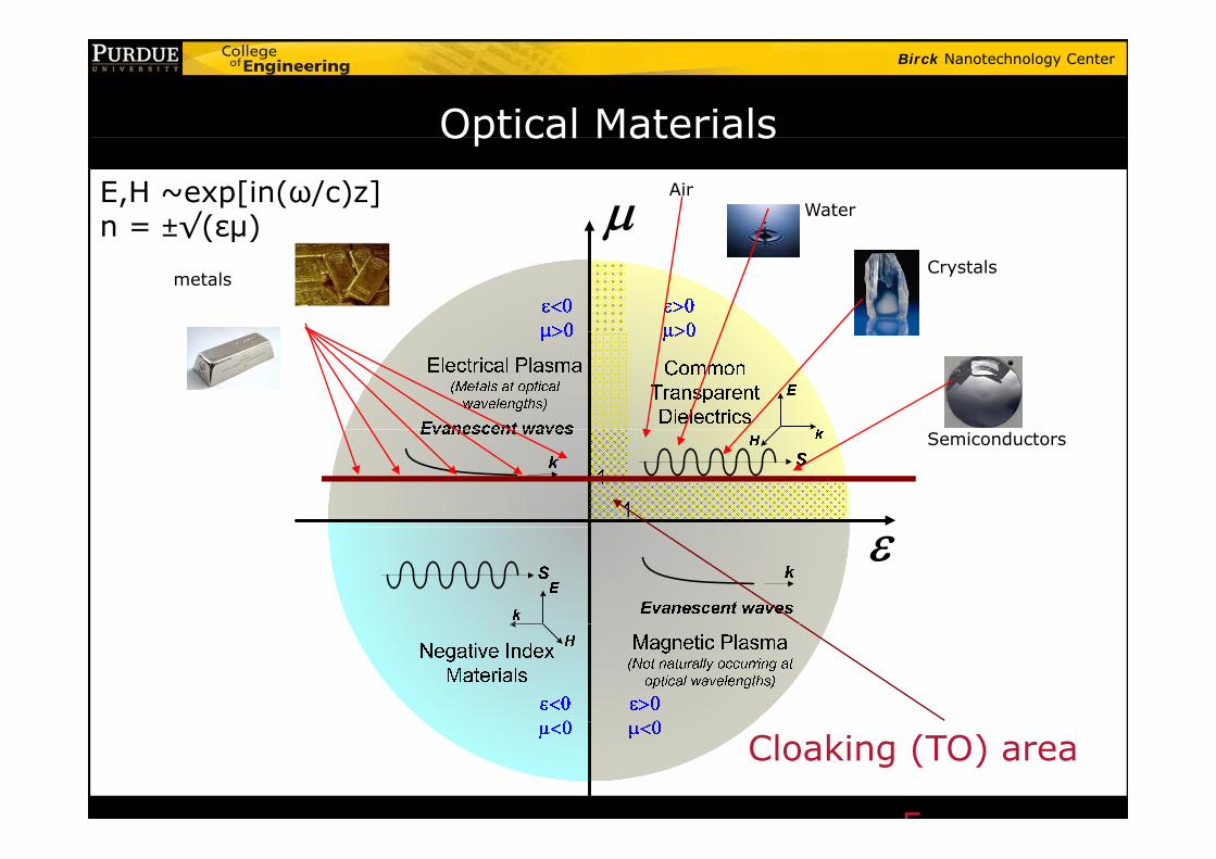
Optical MaterialsOptical Materials
WaterAirE,H ~exp[in(ω/c)z]
n = ±√(εμ)Crystals
metals
n ±√(εμ)
Semiconductors
5
Cloaking (TO) area
Birck Nanotechnology Center
Electrical Metamaterials:Electrical Metamaterials:a route to nanophotonicsp
Birck Nanotechnology Center
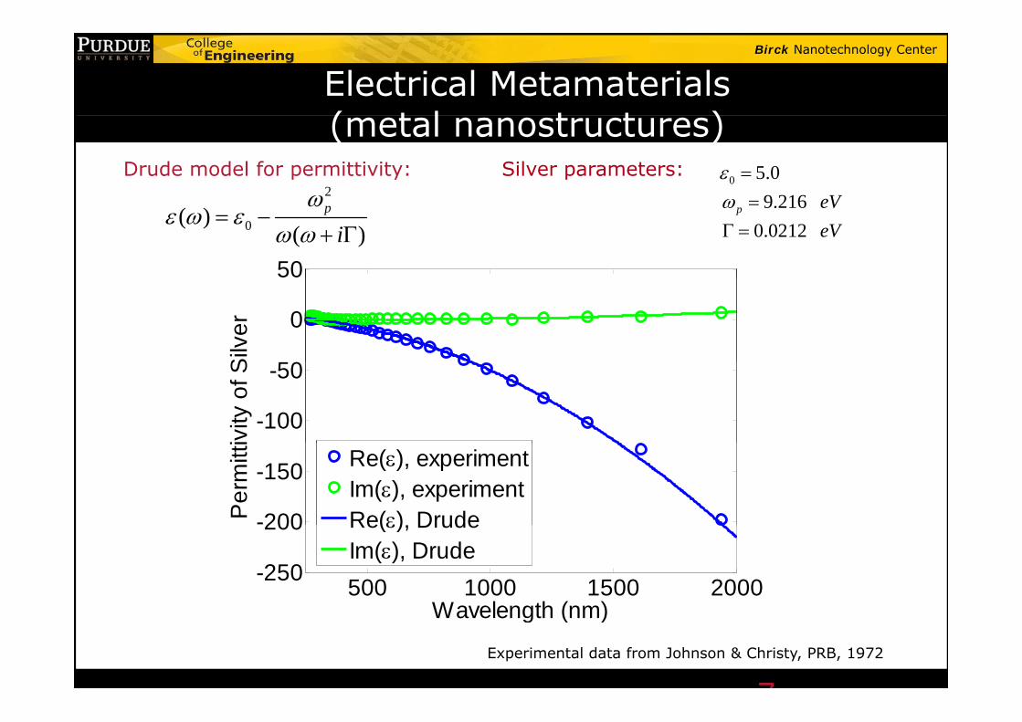
Electrical Metamaterials ( t l t t )(metal nanostructures)
20 5.0
9 216 V Drude model for permittivity: Silver parameters:
50
0( )( )
p
i
9.2160.0212
p eVeV
0
Silv
er
-100
-50
ivity
of S
-200
-150
Per
mitt
i
Re(), experimentIm(), experimentRe() Drude
500 1000 1500 2000-250
200
Wavelength (nm)
Re(), DrudeIm(), Drude
7
Wavelength (nm)
Experimental data from Johnson & Christy, PRB, 1972
Birck Nanotechnology Center
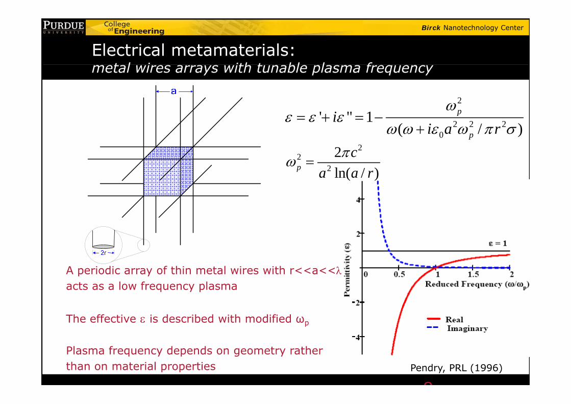
Electrical metamaterials:t l i ith t bl l fmetal wires arrays with tunable plasma frequency
2p
2 2 20
' " 1( / )
p
p
ii a r
2
2 2 c22
2ln( / )p
ca a r
A periodic array of thin metal wires with r<<a<<acts as a low frequency plasma
The effective is described with modified ωp
8
Plasma frequency depends on geometry rather than on material properties Pendry, PRL (1996)
Birck Nanotechnology Center
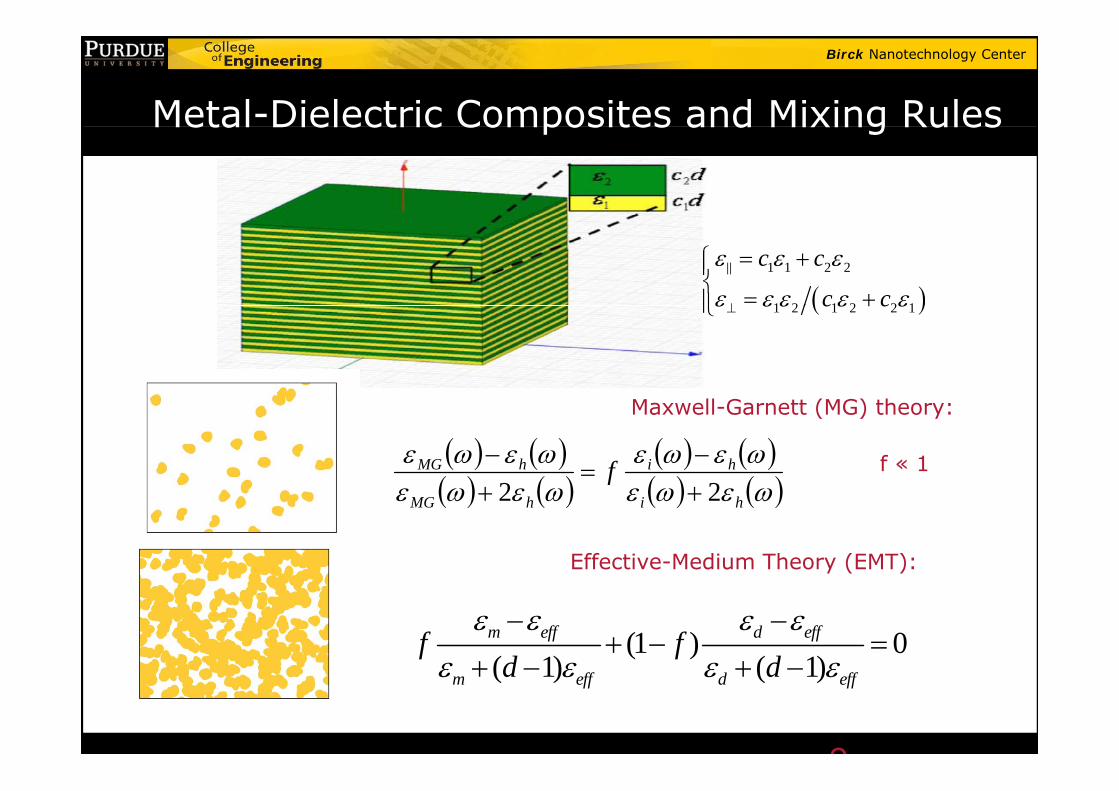
Metal-Dielectric Composites and Mixing RulesMetal Dielectric Composites and Mixing Rules
1 1 2 2
1 2 1 2 2 1
c c
c c
1 2 1 2 2 1c c
hihMG f22
Maxwell-Garnett (MG) theory:
f « 1 hihMG
f22
Effective-Medium Theory (EMT):
(1 ) 0( 1) ( 1)m eff d efff fd d
9
( 1) ( 1)m eff d effd d
Birck Nanotechnology Center
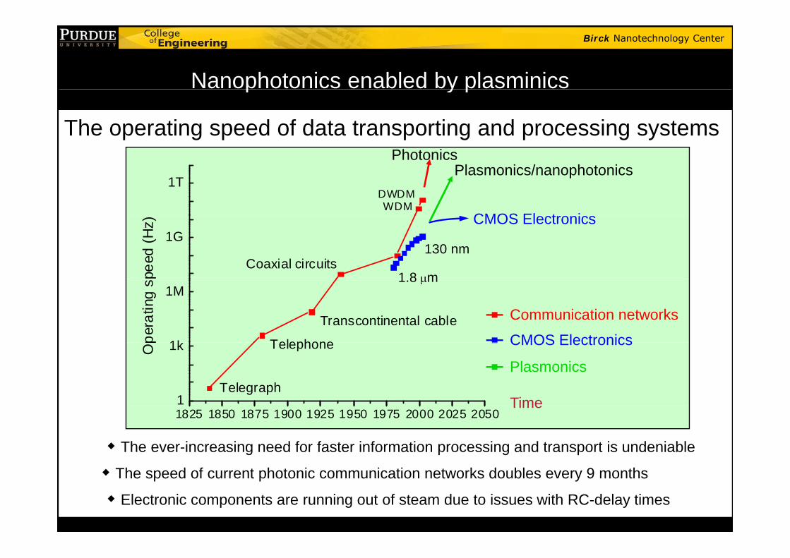
Nanophotonics enabled by plasminics
The operating speed of data transporting and processing systemsPhotonics
p y p
1TDWDMWDM
Plasmonics/nanophotonics
CMOS El t i
Photonics
1G130 nm
1 8 mCoaxial circuits
peed
(Hz) CMOS Electronics
1k
1M1.8 m
Telephone
Transcontinental cable
pera
ting
s
Communication networks
CMOS Electronics
1
1k Telephone
Telegraph
Op
Time
CMOS Electronics
Plasmonics
The ever-increasing need for faster information processing and transport is undeniable
Th d f t h t i i ti t k d bl 9 th
1825 1850 1875 1900 1925 1950 1975 2000 2025 2050Time
The speed of current photonic communication networks doubles every 9 months
Electronic components are running out of steam due to issues with RC-delay times
Birck Nanotechnology Center
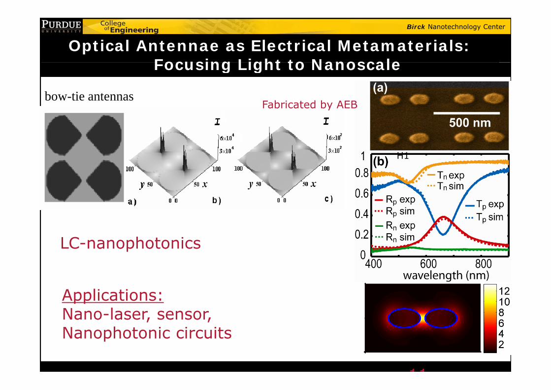
Optical Antennae as Electrical Metamaterials:Focusing Light to NanoscaleFocusing Light to Nanoscale
bow-tie antennasFabricated by AEBFabricated by AEB
H1
LC h t iLC-nanophotonics
Applications:Nano-laser, sensor, N h t i i it
11
Nanophotonic circuits
Birck Nanotechnology Center
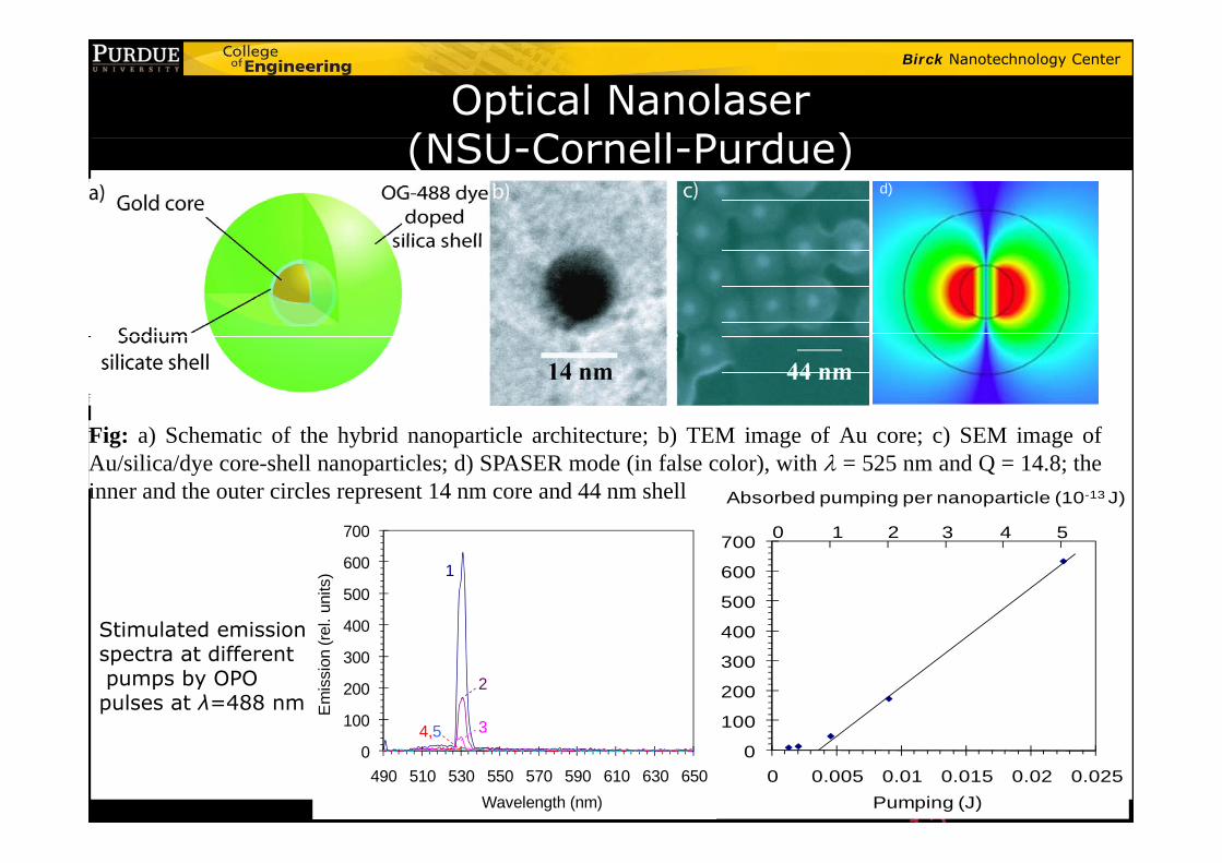
Optical Nanolaser(NSU C ll P d ) (NSU-Cornell-Purdue)
d)
Fi ) S h ti f th h b id ti l hit t b) TEM i f A ) SEM i fFig: a) Schematic of the hybrid nanoparticle architecture; b) TEM image of Au core; c) SEM image ofAu/silica/dye core-shell nanoparticles; d) SPASER mode (in false color), with = 525 nm and Q = 14.8; theinner and the outer circles represent 14 nm core and 44 nm shell Absorbed pumping per nanoparticle (10-13 J)
1 2 3 4 50700
400
500
600
700
. unit
s)
1 2 3 4 50
400
500
600
700
el. u
nits
) 1
Stimulated emission
100
200
300
400
Emiss
ion (r
el100
200
300
400
Em
issi
on (r
e
2
34 5
Stimulated emission spectra at differentpumps by OPO pulses at λ=488 nm
12
0
100
0 0.005 0.01 0.015 0.02 0.025Pumping (J)
0
100
490 510 530 550 570 590 610 630 650Wavelength (nm)
34,5
Birck Nanotechnology Center
Magnetic Metamaterialsf th ti l for the optical range
Birck Nanotechnology Center
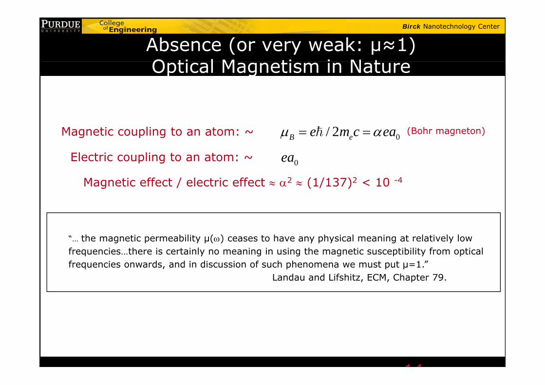
Absence (or very weak: µ≈1) O ti l M ti i N t Optical Magnetism in Nature
Magnetic coupling to an atom: ~ 0/ 2B ee m c ea (Bohr magneton)
0eaElectric coupling to an atom: ~
Magnetic effect / electric effect 2 (1/137)2 < 10 -4
“ th ti bilit ( ) t h h i l i t l ti l l “… the magnetic permeability µ() ceases to have any physical meaning at relatively low frequencies…there is certainly no meaning in using the magnetic susceptibility from optical frequencies onwards, and in discussion of such phenomena we must put µ=1.”
Landau and Lifshitz, ECM, Chapter 79.Landau and Lifshitz, ECM, Chapter 79.
14
Birck Nanotechnology Center
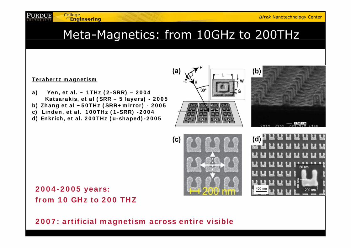
Meta-Magnetics: from 10GHz to 200THzg
Terahertz magnetism
a) Yen, et al. ~ 1THz (2-SRR) – 2004 Katsarakis, et al (SRR – 5 layers) - 2005
b) Zhang et al ~50THz (SRR+mirror) - 2005c) Linden, et al. 100THz (1-SRR) -2004d) Enkrich, et al. 200THz (u-shaped)-2005
2004-2005 years: from 10 GHz to 200 THZ
2007: artificial magnetism across entire visible
Birck Nanotechnology Center
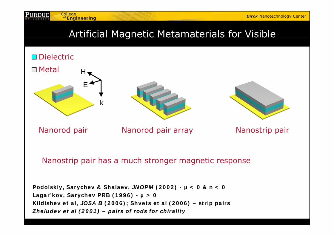
Artificial Magnetic Metamaterials for Visibleg
Dielectric
E
HMetal
k
Nanorod pair Nanorod pair array Nanostrip pair
Nanostrip pair has a much stronger magnetic response
Podolskiy, Sarychev & Shalaev, JNOPM (2002) - µ < 0 & n < 0Lagar’kov, Sarychev PRB (1996) - µ > 0 Kildishev et al, JOSA B (2006); Shvets et al (2006) – strip pairsZheludev et al (2001) – pairs of rods for chirality
Birck Nanotechnology Center
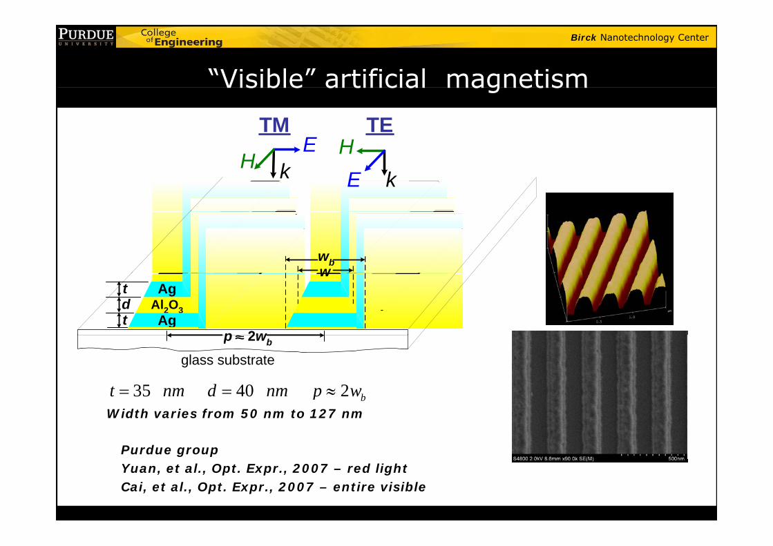
“Visible” artificial magnetismVisible artificial magnetism
ETM
HTE
kE
Hk
HE
wwb
p 2w
tdt
AgAl2O3Ag
w
35 40 2 bt nm d nm p w
glass substrate
p 2wb
bp
Purdue group
Width varies from 50 nm to 127 nm
Yuan, et al., Opt. Expr., 2007 – red lightCai, et al., Opt. Expr., 2007 – entire visible
Birck Nanotechnology Center
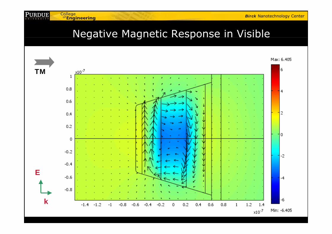
Negative Magnetic Response in Visibleegat e ag et c espo se s b e
TM
EE
k
Birck Nanotechnology Center
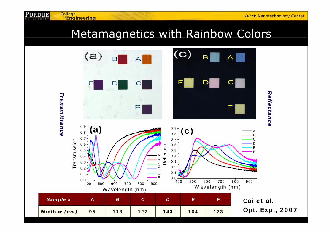
Metamagnetics with Rainbow ColorsMetamagnetics with Rainbow Colors
Tra
nsm
i
Refle
ctan
0 60.70.80.9 (a)
on 0 60 .70 .80 .9
A B CD
(c )
ittan
ce
nce
0.20.30.40.50.6
Tran
smis
sio
A B CD 0 .2
0 .30 .40 .50 .6
Ref
lect
ion D
E F
400 500 600 700 800 9000.00.1
Wavelength (nm)
E F
4 0 0 5 0 0 6 0 0 7 0 0 8 0 0 9 0 00 .00 .1
W a ve le n g th (n m )
Sample # A B C D E F
Width w (nm) 95 118 127 143 164 173
Cai et al.Opt. Exp., 2007
Birck Nanotechnology Center
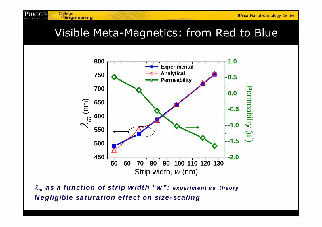
Visible Meta-Magnetics: from Red to BlueVisible Meta Magnetics: from Red to Blue
800 1 0
700
750
800 Experimental Analytical Permeability 0.5
1.0
P
650
700(n
m)
-0.5
0.0
Perm
eab
550
600
m (
1 5
-1.0
bility ('
50 60 70 80 90 100 110 120 130450
500
-2.0
-1.5
')
m as a function of strip width “w”: experiment vs. theory
50 60 70 80 90 100 110 120 130Strip width, w (nm)
m pNegligible saturation effect on size-scaling
Birck Nanotechnology Center
N ti R f ti I d Negative Refractive Index in Opticsin Optics