DES Analysis and Attacks CSCI 5857: Encoding and Encryption.

CHAPTER!
Experimental Techniques and Characterization Tools

This chapter describes about the experimental techniques used for
preparing bulk oxide phosphors and thin film growth. Also analytical tools that
are used to characterize these synthesized phosphors and thin films.
51

Growth techniques do play a significant role in influencing the physico
chemical characteristics of bulk powders as well as thin film materials. It has
been observed that various physical constants, characteristic to a bulk material,
need not remain the same in their corresponding thin films. The structural,
electrical and optical properties of thin films are found to be highly sensitive to
the technique adopted, the substrate chosen, deposition conditions, the presence
of defects and impurities and the film thickness. The appropriate choice of an
experimental technique thereby helps in tailoring a material with controlled,
reproducible and well-defined properties so as to suit a technological
application.
The research work presented in the thesis is focused on development of
oxide phosphors for thin film electroluminescent (TFEL) device applications.
Physical vapour deposition (PVO) techniques such as radio frequency (rf)
magnetron sputtering and pulsed laser deposition (PLO) were used to grow
phosphor thin films. Rf magnetron sputtering was used to deposit thin films of
ZnGa204:Mn, Zn2Ge04:Mn and top insulator (BaTa206) for TFEL device
fabrication. PLO was used to grow high quality thin films of Y 203:EU3+ on
amorphous substrate. Thermal evaporation was used to deposit metal electrodes
(aluminum) to complete the device structure with top electrical contact. The
present chapter discusses the various methodologies adopted for bulk phosphor
synthesis and thin film growth. It also briefs on the different analytical
techniques used in the present study.
2.1. Bulk synthesis techniques
The targets for both sputtering and PLD techniques, were synthesized in
the laboratory from highly pure starting materials. Powder target of

Chapter 2------------------------------------------------------
ZnGa204:Mn2+, Zn2Ge04: Mn2+ was used for sputter deposition. A one inch
pellet ofY203:Eu3+ was used as the target for the laser ablation.
For preparing bulk ZnGa204:Mn2+, Zn2Ge04:Mn2+ powders and the
powder target for sputtering, stoichiometric quantities of the starting materials
were thoroughly mixed in alcohol medium and fired in a high temperature
furnace (l350oe for ZnGa204:Mn2+ and 12000e for Zn2Ge04:Mn2+) for a fixed
time of 12 hrs.
A two-step firing process is usually adopted for Y 203:Eu3+ pellet
synthesis. The constituent materials, after thorough mixing, are calcined at
1200°C. This powder with some suitable amount of binder (Poly vinyl alcohol)
is then pressed into a one inch diameter pellet using a hydraulic press on
applying a force of 3 tons. The pellet is then sintered to ensure denser pellet for
better thin film growth. During sintering, the temperature is to be raised in steps
to completely remove moisture from the target. Moisture, if trapped inside the
target, leads to cracking during firing. Normally, the outer part of a target heats
up faster than the inner part. If the temperature were increased too quickly from
room temperature to the high processing temperature, the outer part of the target
would become dense before the moisture in the inner part escapes. So the pellet
is slowly heated to lOOoe and kept there for some time to ensure the whole water
has been evaporated. Since we add binder which is an unwanted impurity,
should be removed. Nonnally PV A evaporates at 300°C. So the pellet is now
slowly heated to 3000e and kept at this teperature for some time to ensure the
evaporation of binder. The sintering temperature, 1500°c is attained through a
series of steps with the help of a programmable furnace. In the present study,
Y20 3: Eu3+ was sintered at 1 500°C for 48 hrs in air.
54
--------------Experimental techniques and characterization tools
2.2. Thin film growth techniques
A 'thin film' has one of its linear dimensions very small compared to the
other two and is characterized by a large surface to volume ratio. Any thin film
deposition process involves the following sequential steps [1]:
Transition of the condensed phase (solid or liquid) into the gaseous state
(atomic/molecular/ionic species)
Transport of the vapor from the source to the substrate
Condensation of the vapor upon arrival on the substrate
The deposition techniques are broadly classified into two - physical and
chemical - depending on how the atoms/molecules/ions/clusters of the species
are created for condensation process. Various chemical methods have been
realized for thin film deposition of phosphor materials. Some of them are sol-gel
synthesis [2,3], solvent evaporation epitaxy method [4], electrophoresis [5],
spray pyrolysis [6,7] and dip-coating [8]. Thennal and electron-beam
evaporation, pulsed ion-beam evaporation [9], chemical vapor deposition (CVO)
[10], PLD, rf sputtering, and atomic layer epitaxy (ALE) falls under the stream
of physical methods generally adopted for thin film phosphor growth. The
following sections briefs the various thin film deposition techniques used in the
present work.
2.2.1 Thermal evaporation by resistive heating
Thennal evaporation is a simple and convenient technique widely used
for the deposition of thin films of metals, alloys and many compounds. The
process, in general, involves heating up of a source material until it evaporates
and condenses on a cold target surface, referred to as the substrate. If carried out 55
Chapt~2------------------------------------------------------
in vacuum, the evaporation temperature can be considerably lowered and the
formation of oxides and incorporation of impurities in the growing layer can be
avoided. Moreover, at pressures as low as 10-6 or 10-5 Torr, the mean free path of
vapor atoms shall be of the same order as the vacuum chamber dimensions.
Hence, the particles can travel in straight lines from the evaporation source
towards the substrate without being significantly scattered [Ill-
In thermal evaporation technique, the average energy of vapor atoms
reaching the substrate surface is generally low (of the order of kT, ie. tenths of
eV)_ Here, a refractory metal (tungsten or tantalum) strip or shaped filaments
are heated directly by attaching the ends to a low-voltage, high-current
supply to evaporate the charge. The characteristics and quality of the deposited
film shall depend on the substrate temperature, rate of deposition, ambient
pressure, etc. The homogeneity of the film depends on the geometry of the
evaporation source and the distance from the source material to the substrate.
Excellent and detailed reviews on the know-how of the technique have been
discussed by Holland [12].
In the present work, the deposition of metal electrodes (AI) was done
using thermal evaporation via resistive heating.
2.2.2 Sputtering
Sputter deposition is one of the most widely used techniques for the
fabrication of thin-film structures. In 1852 Sir W.R. Grove discovered surface
coatings generated in the valve. It was called as 'Spluttering', meaning the
generation of drop out of a liquid surface by an impinging primary drop. The
expression' Sputtering' was a printer'S error but was soon adopted as a scientific
term. Sputtering is one of the most widely used technologies to prepare thin 56

--_____________ Experimental techniques and characterization tools
films. In sputter deposition, material is removed - as atoms or molecules - from a
solid target by energetic ion bombardment and deposited as atomic layers on a
substrate. By applying a high RF or DC voltage between the target (cathode) and
the substrate (anode), energetic electrons emitted from the target form ions in the
process gas, typically argon at 1 to 100 mTorr pressure. Under these conditions,
plasma - a partially ionized gas - is formed. When a target is sputtered with ions,
following phenomena may occur. 1) The ions may get reflected, probably being
neutralized in the process. This reflection is the basis of technology known as
ion scattering spectroscopy. 2) The impact of the ion may cause the target to
eject an electron, usually referred as secondary electrons. 3) The ion may
become buried in the target-known as ion implantation. 4) The ion impact may
also responsible for some structural rearrangements in the target material.
Rearrangements include simple vacancies and interstitials or more gross lattice
defects such as change in stoichiometry in the case of alloys and compound
targets.5) The ion impact may set up a series of collisions between the atoms of
the target, possibly leading to ejection of atoms known as sputtering.
A DC sputtering system cannot be applied to insulator target, because of
the immediate build up of positive charge at the surface of target. In order to
sustain the glow discharge with an insulator target, rf power should be applied.
RF sputtering process operates on the order of megahertz, usually 13.56 MHz,
the frequency allotted by international communication authorities. When an rf
power is applied to the target, electrons which could exist in the sputtering gas,
or could be emitted from the target or chamber wall, are discharged and
scattered with sputtering gas, according to current between target and ground. In
this process some of the Ar ions are also get ionized. According to rffrequency,
57

Chaprer2------------------------------------------__________ __
the electrons are accelerated and travel between the electrodes (ground and
target). Since Ar atoms are heavier compared to electrons, Ar ions cannot
respond to the frequency and therefore oscillates only in short distances. Due to
this effect operating pressure to achieve plasma in rf sputtering is lower than that
in dc sputtering. Also sputtering yield gets improved. In the case of magnetron
sputtering, since electrons are confined around the target, they get more chance
to collide with Ar atom, thereby increasing Ar ion plasma to sputter the target.
The secondary electrons emitted from the target sustain the plasma near the
target. Therefore operating pressure could be reduced further. Since the surface
area of the target is less than the ground or the wall of the chamber, the
configuration of the electrodes is asymmetric. Due to this asymmetric
configuration of the electrodes and mobility difference between electrons and
ions, target is displaced to a negative potential with a mean known as dc offset
which induces sputtering. Therefore target will acquire a self-bias and will have
a value equal to half of the applied rf peak to peak voltage. This dc offset will
give rise to sputtering at the target. The rf voltage that gives rise to sputtering
will be a function of pressure inside the chamber and the current will be
proportional to the ion flux. In 1935 Penning first studied and low pressure dc
magnetron sputtering in a system that was composed of coaxial cylindrical
electrodes with an axial magnetic field. But these kinds of systems are not used
in practice. In the early 1960s, magnetron sputtering was reconsidered as an
attractive process for thin film deposition. Gill and Kay proposed an inverted
magnetron sputtering system and demonstrated that the sputtering gas pressure
was as low as 10-5 Torr [13]. Kesaer and Pashkova [14] gave the basic idea of
58
- ______________ Experimental techniques and characterization tools
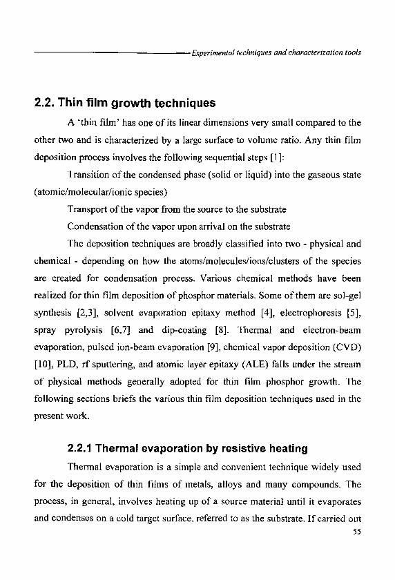
the planar magnetron sputtering, and Hayakawa and Wasa [15] invented an early
planar magnetron sputtering system with a solenoid coil.
Figure 2.1 Schematic diagram of sputtering process
Nowadays, the planar type using permanent circular magnets is widely
used because of such advantages as its simple structure, suitable adaptation, and
wide coating area in spite of the disadvantage of the localized erosion of target
that causes the deposition rates to change over a period of time.
2.2.3 Sputtering Parameters
a) Sputtering gas
Noble gases are usually used in sputtering due to their chemical
inactivity. Among them Ar is a better choice as it is cheaper and has sputtering
yield 'two' down on Xe and Kr. The glow discharge is sustained by electrons 59

Chaprer2--------------------------------------------------------
making collisional ionizations with Ar gas. Therefore increasing Ar pressure will
increase the sputtering yield. A different problem however exists at higher
pressures. The material which is being sputtered collides with the Ar ions/gas
atoms on its way to the substrate which will decrease the sputtering yield. So
there is an appropriate pressure, for which, sputtering yield is a maximum. This
is determined by the size and geometry of chamber and gun. The space between
ground and target electrodes should be designed not to be narrow or labyrinthine
for Ar gas to diffuse easily and quickly. We get stoichiometric films in reactive
sputtering due to this reason. The reaction will be taking place at both target
surface and substrate during deposition. In this case maximum sputtering yield is
obtained when reaction time equals sputtered time. In order to deposit oxides,
we use oxygen as reactive gas. In planar configuration, optimum concentration
of reactive gas is determined by NglNt > 1 for reaction at target, and NglNs > 1
for reaction at substrate, where Ng is the number of reactive gas molecules
which strike unit area of target/substrate per unit time, Nt is number of sputtered
atoms per unit area of the target per unit time and Ns is number of deposited
atoms per unit area of the substrate per unit time. The minimum oxygen partial
pressure can be calculated from the above relations. However in practice
optimum partial pressures can be found out by trial and error experiment. If the
reaction takes place at the target, sputtering yield is reduced. So the gas inlets of
sputtering gas and reactive gas are separated from each other inside the chamber.
For example a relatively big ground shield surrounds the target and the
sputtering gas is injected through the inlet near to the target at higher pressure
than the reactive gas. And by putting the reactive gas inlet near the substrate, the
reaction can be improved with a relatively high deposition yield.
60
--_____________ Experimental techniques and characterization tools
b) Sputtering Power
For each operating pressure, target material and sputtering gas,
there is a specific voltage-current relationship. Actually target material is not
that important even though the secondary electron coefficient varies from target
to target. Under similar conditions current densities are very much alike, except
for some conducting targets. The sputtering rate of the target is determined by
the flux of ions and energetic neutrals and hence the sputtering yield. An ion
current of lmAlcm2 corresponds to a flux of 6xlOI5 singly charged ions per
cm2/sec. The sputtering yield rises monotonically with ion energy up to several
tens of KeV, where it begins to decrease. This upper limit of ion energy is
dependent on target material. Electrically we would like low voltages and
because x-rays can be produced by fast ions and electrons we ought to keep
energies and voltages below lOKV. In order to transfer the power to the target it
is necessary to minimize the impedance between the power supply and target.
Thus electric connectors with low capacitance must be used and good electric
shields are required in order not to leak the rf power. During the deposition of
the film, the impedance changes due to the deposition onto the walls of the
chamber and the ground shield. Hence adjustments are sometimes necessary. It
is very important for the deposition of the oxides and nitrides whose resistance is
very large.
c) Ground shields
The purpose of ground shield, or dark space shield, is to restrict ion
bombardment to the target and sputtering to the target only. Otherwise the target
backing plate, mounting clips and mechanical supports would also be sputtered
and films get contaminated. In order to prevent ion bombardment of the
61

Chaprer2------------------------------------------------------
protected regions, the space between the target and ground shield must be less
than the thickness of the dark space. This criterion is such as to prevent the
establishment of self-sustained discharge in the space between the target and
shield. Occasionally one finds that sharp points or patches of dirt cause local
discharges or arcs, particularly with dc discharges, and these should be
eliminated. Since the thickness of the dark space decreases with increase in
pressure, size of the gap between target and shield sets an upper pressure limit
for operating the system. In principle, the gap should be extremely small, but in
practice it is limited by spurious discharges and in case of rf discharges, by
increasing capacitive target to ground coupling as the gap is decreased which
will result in serious loss of electric power. The dark space thickness also
decreases with frequency too. So systems operating above 13.56 MHz need to
have correspondingly closer ground shields. Generally 2-3 mm of the target
ground separation is reasonable.
d) Target cooling
Sputtering is a very inefficient process and most of the power input to
the gun appears finally as target heating. Such heating can become excessive -
local temperatures of 400°C have been reported and can lead to damage of the
bonding between the target and backing electrode' of the target itself and
associated O-rings etc. This is usually avoided by cooling the target with water
or another suitable liquid. On the other hand such cooling is complexity and it
can be avoided if the power input to the target is not too great. When water is
used as coolant, electric current leaks through water. Hence the resistance of
water must be high enough. In this sense de-ionised water is the best choice. In
62

--____________ Experimental techniques and characterization tools
general, with the sputtering gun, the permanent magnets sit in the cooling water
to prevent the magnets from losing magnetic field due to over heating.
e) Control of sputtering parameters
The sputtering parameters can be controlled for optimized thin film
quality. McMahon et al. have developed a fully computerized planar sputtering
system for thin film deposition for AIN [16]. They had deposited films under
adequate partial pressures of argon and nitrogen gases under following
conditions. 1) Control of gas flows under constant rf powers; 2) Control of rf
power under constant gas flows; 3) control of target rf voltage instead of rf
power under constant gas flows. They reported that the third method was most
stable and the films developed in this condition were best. This is an important
fact in sputtering deposition. During deposition due to change in impedance
between the target and ground shields or the wall of the chamber, the current is
changed for a constant power. Therefore instead of controlling the power, it is
important to control the target voltage, which accelerates the ions. This result
can be applied when oxide films are deposited as well as pure semiconductors.
The advantages of sputtering over evaporation techniques are:
• higher kinetic energy of deposited atoms results in better film adhesion;
• more easily automated for in-line industrial processing;
• no 'spitting' occurs that would leave cluster of material on the substrate;
• sputter source can be mounted in any orientation;
• plasma is energetically hot, but has a small thermal capacity;
• since coverage is independent of line-of-sight, sputtering inherently
produces uniform film coatings over non-flat surfaces;
63

Chapter 2---------------------------
• refractory materials, elements, mixtures and alloys can be sputtered with
equal facility;
• most importantly, sputtering with oxygen (or nitrogen) in the argon
process gas leaves the target unreacted, yet deposits an oxide (or nitride)
film on the substrate.
This last advantage is often used to produce nonconductive film, since
'reactive' DC sputtering of a metal allows higher deposition associated with RF
sputtering.
2.2.4 Pulsed laser deposition (PLO)
In material science, lasers play a significant role either as a passive
component for process monitoring or as an active tool by coupling its radiation
energy to th@ material being processed, leading to various applications such as
localized melting during optical pulling, laser annealing of semiconductors,
surface cleaning by desorption and ablation, laser induced rapid quench to
improve surface hardening and most recently pulsed laser deposition (PLO) for
growing thin films [17]. PLO is the deposition method of choice when one needs
to deposit materials with complex stoichiometry. PLO was the first technique
successfully used to deposit a superconducting YBa2CU307-d thin film. Since
then, many materials, especially multi-element oxides, normally difficult to be
deposited by other methods, have been deposited by PLO. This technique offers
many potential applications, from integrated circuits and optoelectronics to
micro mechanics and medical implants [18].
In a typical PLO process, a focused train of high energy laser pulses,
derived from a UV nanosecond pulsewidth laser source, such as the frequency
tripled (355 nm) or quadrupled (256 nm) solid state Nd:Y AG laser, or the KrF 64

--------------Experimental techniques and characterization tools
(248 nm) or ArF (193 nm) excimer laser, is rastered over either a metal, a single
crystal oxide, or a compressed oxide powder target in a vacuum chamber. The
high pulse energy beam-target interaction creates a plume comprised of atomic
and molecular species ablated from the target. A substrate, often heated, is
placed at a short distance from the target in the direction of the advancing plume
(figure 2.2). Though the actual physical process of material removal is quite
complex, one can consider the ejection of material, to occur from rapid
explosion of the target surface by superheating. Unlike thermal evaporation,
which produces a vapor composition dependent on the vapor pressures of
elements in the target material, the laser-induced expulsion produces a plume of
material with stoichiometry similar to the target.
The best quality films can be deposited by controlling the fundamental
criteria such as the substrate temperature, the relative and absolute arrival rates
of atoms and the energy of the depositing flux. PLD offers the best control over
these criteria than other vacuum deposition techniques [19].
The main advantages of pulsed laser deposition are:
• conceptually simple: a laser beam vaporizes a target surface,
producing a film with the same composition as the target.
• versatile: many materials can be deposited in a wide variety of gases
over a broad range of gas pressures .
• cost-effective: one laser can serve many vacuum systems.
• fast: high quality samples can be grown reliably in 10 or 15 minutes.
• scalable: as complex oxides move tOWard volume production.
65

Chapter 2--------------------______ _
n
Target carrousel
laser beam
Vacuum chamber
Figure 2.2 Schematic diagram of PLO chamber
The mechanism of pulsed laser deposition, in contrast to the simplicity
of the set-up, is a very complex physical phenomenon. It not only involves the
physical process of the laser-material interaction, but also the formation plasma
plume with high energetic species and even the transfer of the ablated material
through the plasma plume onto the substrate surface. Thus the thin film
formation in PLD generally can be divided into the following four stages.
1. Laser radiation interaction with the target
2. Dynamics of the ablated materials.
3. Deposition of the ablation materials on the substrate.
4. Nucleation and growth of a thin film on the substrate surface
66

--____________ Experimental techniques and characterization tools
Each stage in PLO is critical to the fonnation of quality epitaxial,
crystalline, stoichiometric and unifonn thin films.
In the first stage, the laser beam is focused onto the surface of the target.
At sufficiently high flux densities and short pulse duration, all elements in the
target are rapidly heated up to their evaporation temperature. Materials are
dissociated from the target surface and ablated out with stoichiometry as in the
target. The instantaneous ablation rate is highly dependent on the fluence of the
laser shining on the target. The ablation mechanisms involve many complex
physical phenomena such as collisional, thennal, and electronic excitation,
exfoliation and hydrodynamics.
During the second stage the emitted materials tend to move towards the
substrate according to the laws of gas-dynamics and show the forward peaking
phenomenon. The spatial thickness varies as a function of cose. The spot size of
the laser and the plasma temperature has significant effects on the deposited film
unifonnity. The target-to-substrate distance is another parameter that governs the
angular spread of the ablated materials. A mask placed close to the substrate
could reduce the spreading. Typical plasma temperature measured by emission
spectroscopy during initial expansion of the plume is :::::: 10,000 K, which is well
above the boiling point of most materials (:::::: 3000 K). Heating of the plasma to
these temperatures is thought to occur by inverse--Bremsstrahlung absorption of
the laser light in a free - free transition of electron ion pair. This high
temperature would evaporate the surface layer of the target thereby producing
exact composition in the thin films.
The third stage is important to detennine the quality of thin film. The
ejected high-energy species impinge onto the substrate surface and may induce
67

Chapter 2---------------------------
various type of damage to the substrate. These energetic species sputter some of
the surface atoms and a collision region is formed between the incident flow and
the sputtered atoms. Film grows after a thermalized region is formed. The region
serves as a source for condensation of particles. When the condensation rate is
higher than the rate of particles supplied by the sputtering, thermal equilibrium
condition can be reached quickly and film grows on the substrate surface at the
expenses of the direct flow of the ablation particles and the thermal equilibrium
obtained.
The effect of increasing the energy of the adatoms has a similar effect of
increasing substrate temperature on film growth [19]. Typical power densities
involved in PLD are approximately 50 MWcm-2 for a reasonable growth rate. (>
1 A o/shot) If plasma is formed during laser target interaction in vacuum or in air
then an explicit laser - plasma interaction occurs due to which ions in the plasma
are accelerated to as much as 100 - 1000 eV [18]. Nucleation-and-growth of
crystalline films depends on many factors such as the density, energy, ionization
degree, and the type of the condensing material, as well as the temperature and
the physico-chemical properties of the substrate. The two main thermodynamic
parameters for the growth mechanism are the substrate temperature T and the
supersaturation Dm related by the following equation:
(2.6)
where, k is the Boltzmann constant, R is the actual deposition rate, and
Re is the equilibrium value at the temperature T.
The nucleation process depends on the interfacial energies between the
three phases present - substrate, the condensing material and the vapour. The
critical size of the nucleus depends on the driving force, i.e. the deposition rate
68

--------------Experimental techniques and characterization tools
and the substrate temperature. For the large nuclei, a characteristic of small
super-saturation, they create isolated patches (islands) of the film on the
substrate, which subsequently grow and coalesce together. As the super
saturation increases, the critical nucleus shrinks until its height reaches on
atomic diameter and its shape is that of a two-dimensional layer. For large super
saturation, the layer-by-layer nucleation will happen for incompletely wetted
foreign substrates.
The crystalline film growth depends on the surface mobility of the
adatom (vapour atoms). Normally, the adatom will diffuse through several
atomic distances before sticking to a stable position within the newly fonned
film. The surface temperature of the substrate detennines the adatom's surface
diffusion ability. High temperature favours rapid and defect free crystal growth,
whereas low temperature or large supersaturation crystal growth may be
overwhelmed by energetic particle impingement, resulting in disordered or even
amorphous structures.
The mean thickness (N99) at which the growing thin and discontinuous
film reaches continuity, is given by the formula:
N99 = A(11R)1I3 exp(-lfT) (2.7)
where A is a constant related to the materials r 18]. In the PLD process,
due to the short laser pulse duration (~1 0 ns) and hence the small temporal
spread (:::;10 ms) of the ablated materials, the deposition rate can be enonnous
(~10 nm/s). Consequently a layer-by-layer nucleation is favoured and ultra-thin
and smooth film can be produced. In addition, the rapid deposition of the
energetic ablation species helps to raise the substrate surface temperature. In this
69

Chapter 2----------------------____ _
respect, PLO tends to demand a lower substrate temperature for crystalline film
growth.
In the present study, PLO was used to deposit Y20 3: Eu3+ phosphor
films. Pulsed laser deposition of thin films was carried out in a vacuum chamber
pumped by a turbo-molecular pump (Pfeiffer Vacuum Inc, Gennany). The laser
used was the fourth hannonics (266 nm) of Nd:Y AG laser (Spectra Physics
model LAB 170).
2.3 Device Fabrication
Alternating current thin film electroluminescent (ACTFEL) devices can
be fabricated in vacuum and non-vacuum environments. Practical TFEL devices
are expensive as a consequence of using vacuum assisted techniques for film
growth. To reso.lve the problem of cost, new techniques have been explored to
eliminate the need for vacuum processes. As oxide phosphors are less moisture
sensitive, solution coating techniques [20] and sol-gel synthesis [21] can be used
for fabricating devices.
In the present work, rf magnetron sputtering was used to deposit the
light emitting layer and the top insulating layer of the fabricated ACTFEL
devices. The top electrode was thermally evaporated onto the device to complete
the standard metal-insulator-semiconductor-insulator-metal (MISIM) structure.
Commercially available Ohara (supplied by Planar Inc.) and nippon electric
glass (NEG) substrates coated with indium tin oxide (ITa) and aluminium
titanium oxide (ATO) were used for device fabrication. These substrates could
withstand a temperature of up to a maximum of 650°C.
70

--____________ Experimental techniques and characterization tools
2.4 Characterization tools
Once the films are grown, the structural, compositional, morphological,
optical and electrical analytical tools give a better understanding of the film
properties. On the reverse, the characterization techniques help in optimizing the
growth conditions to get device quality films. In the following sections, the
techniques used for the film characterizations in the present study are discussed
briefly.
2.4.1 Thin film thickness
Film thickness has a crucial role in determining its properties
unlike a bulk material. The properties of the thin films can be reproduced if
thickness, along, with other deposition parameters, is kept constant. Film
thickness may be measured either by in-situ monitoring of the rate of deposition
or after the film deposition. The thicknesses of the thin films prepared for the
work presented in this thesis were measured by a stylus profiler (Dektak 6M).
The stylus profiler takes measurements electromechanically by moving
the sample beneath a diamond tipped stylUS. The high precision stage moves the
sample according to a user defined scan length, speed and stylus force. The
stylus is mechanically coupled to the core of a linear variable differential
transformer (LVDT). While in contact over the moving sample surface, surface
variations cause the stylus to be translated vertically. Electrical signals
corresponding to the stylus movement are produced as the core position of the
L VDT changes. The L VDT scales an ac reference signal proportional to the
position change, which in turn is conditioned and converted to a digital format
through a high precision, integrating, analog-to-digital converter [21].
71

Chaprer2------------------------------------------------------
To measure the film thickness, a region of the substrate has to be
masked during film deposition. This creates a step on the sample. The thickness
of the sample can then be measured accurately by measuring the vertical motion
of the stylus over the step.
2.4.2 Structural Characterization
The crystallographic nature of a sample very well influences its
electrical and optical properties. The structural characterization of the bulk and
thin film samples were done in the present study by recording the x-ray
diffraction (XRD) pattern. Any material has a characteristic diffraction pattern,
whether present in pure state or as one the constituent of a mixture of substances.
This fact is made useful in the diffraction method of chemical analysis. The
advantage of XRD analysis is that it discloses the presence of a substance, as
that substance actually exists in the sample and not in terms of its constituent
chemical elements. Hence, diffraction analysis is useful whenever it is necessary
to know the state of chemical combination of the elements involved or the
particular phase in which they are present. Compared with ordinary chemical
analysis the diffraction method has the advantage that it is usually much faster,
requires only very small quantity of sample and is non destructive [22].
The basic law involved in the diffraction method of structural analysis is
the Bragg's law. When monochromatic beam of x-rays impinge upon the atoms
in a crystal lattice, each atom acts as a scattering source. The crystal lattice
presents a series of parallel reflecting planes to the incident x-ray beam. The
intensity of the reflected beam at certain angles will be maximum when the path
difference between two reflected waves from two different crystal planes is an
integral multiple 00 .. This condition is termed as Bragg's law and is given by,
72
--____________ Experimental techniques and characterization tools
n1.;;;; 2dsin9 (2.8)
where, n is the order of diffraction, A is the wavelength of x~rays, d is
the spacing between consecutive parallel planes and 9 is the glancing angle (or
the complement of the angle of incidence) [23].
X~ray diffraction studies give a whole range of information
about the crystal structure, orientation, average crystalline size and stress in the
powder. Experimentally obtained diffraction patterns of the sample are
compared with the standard powder diffraction files published by the
International Centre for Diffraction Data (lCDD).The average grain size of the
film can be calculated using the Scherrer's formula [22],
d = 0.91. ~cose
(2.9)
where, A is the wavelength of the x~ray used and ~ is the full width at
half maximum in radians. The lattice parameter values for different
crystallographic systems can be calculated from the following equations using
the (hkl) parameters and the interplanar spacing d.
Cubic system, (2.10)
Tetragonal system, (2.11)
Hexagonal system, (2.12)
Orthorhombic system, (2.13)
73

Chapwr2------------------------------------------------------
X-ray diffraction measurements of the samples in the present studies
were done using Rigaku automated x-ray diffractometer. The filtered
copper Ka radiation (A. = 1.5418Ao) was used for recording the
diffraction pattern.
2.4.3 Morphological analysis
Surface morphology is an important property while going for
multilayer device fabrication. Roughness of the thin film surface plays a vital
role, especially while making interfaces. Some of the characterization tools used
to study about the surface of thin films is described below.
(a) Scanning electron microscope (SEM)
The scanning electron microscope (SEM) uses electrons rather
than light to form an image. SEM has several advantages over an ordinary light
microscope [24). The SEM has a large depth of field, which allows a large
amount of the sample to be in focus at a time. The SEM also produces images of
high resolution, which means that closely spaced features can be examined at a
high magnification. Preparation of the samples is relatively easy since mi)st
SEMs only require that sample should be conductive. The combination of higher
magnification, larger depth of focus, greater resolution, and ease of sample
observation makes the SEM one of the most heavily used instruments in current
research areas.
In a typical SEM, electrons are thermionically emitted from a tungsten
or lanthanum hexaboride (LaB6) cathode and are accelerated towards an anode.
Alternatively, electrons can be emitted via field emission. The most common is
the Tungsten hairpin gun. 74

--_____________ Experimental techniques and characterization tools
Two components or the magnetic field B
BR = Longitudinal component(down the axis)
BL = Radial compment (perpendirular to the axis)
Figure 2.3 The focusing of electrons in SEM
Tungsten is used because it has the highest melting point and lowest
vapour pressure of all metals, thereby allowing it to be heated for electron
emission. A voltage is applied to the loop, causing it to heat up. The anode,
which is positive with respect to the filament, forms powerful attractive forces
for electrons. This causes electrons to accelerate toward the anode. The anode is
arranged, as an orifice through which electrons would pass down to the column
where the sample is held.
The electron beam, which typically has an energy ranging from a few
hundred eV to 100 keY, is attracted through the anode are made to pass through
a condenser lens, and are focused to very fine point on the sample by the
75

Ch~rer2----------------------------------------__________ --
objective lens (figure 2.3). The electron beam hits the sample, producing
secondary electrons from the sample. These electrons are collected by a
secondary detector or a backscatter detector, converted to a voltage, and
amplified. The amplified voltage is applied to the grid of the CRT that causes the
intensity of the spot of light to change. The image consists of thousands of spots
of varying intensity on the face of a CRT that correspond to the topography of
the sample.
The spatial resolution of the SEM depends on the size of the electron
spot, which intum depends on the electron energy and the magnetic electron
optical system which produces the scanning beam. To ensure that the
information recorded in the image arises only from the sample surface. the..
column must always be at vacuum. Or else, there are chances for contamination
of the sample and the electron beam, instead of being directed onto the sample,
would induce ionization in any background gas that would effect the
measurement being made on the sample. In the present thesis, JEOL JSM 5600
was used for SEM analysis.
(b) Atomic force microscope (AFM)
The atomic force microscope (AFM) is a very high-resolution
type of scanning probe microscope, with resolution of fractions of a nanometer,
more than 1000 times better than the optical diffraction limit. It can, therefore,
probe into understanding the fine details of a sample surface [25]. In atomic
force microscopy, a tip, integrated to the end of a spring cantilever, is brought
within the interatomic separations of a surface, such that the atoms of the tip
and the surface are influenced by interatomic potentials. As the tip is rastered
across the surface, it bounces up and down with the contours of the surface. 76

---___________ Experimental techniques and characterization tools
Feedback Amplifier
Mill'Of
TIp --__ nII"~
Sample
Figure 2.4 The essential elements of an AFM
By measuring the displacement of the tip (i.e. the deflection of the
cantilever), one can theoretically map out the surface topography with atomic
resolution. The AFM is essentially identical in concept to the scanning
profilometer, except that the deflection-sensitivity and resolution are improved by
several orders of magnitude. The AFM can operate well in ambient air or in a liquid
environment making it an important tool in studying biological systems, polymers and
a host of insulator and semiconductor materials.
An AFM images a surface in a manner analogous to the gramophone
stylus sensing the groves of gramophone disk. The essential elements of an
AFM are shown in the figure 2.4. The tip is attached to a cantilever type spring
as shown in the figure 2.5. As the tip and sample interact, forces act on the tip
and cause the cantilever (spring) to deflect. The cantilever position is monitored
by a position detector. The output of the detector is connected to a feedback
controller that regulates the force between the sample and the tip by moving the
sample up or down. The sample is moved by a PZT scanning actuator. The 77

Chapter 2--------------------______ _
cantilever must be soft enough to deflect a measurable amount without
damaging the surface features of the sample.
The amount of deflection js proportional to the force acting on the tip
Fspring = -k·/lZ (2.14)
where F is the force on the sample, k is the spring constant of the cantilever, and,
tU, is the deflection of the cantilever.
Sur10ce
cantIever
.6~Probe ~
Figure 2.5 Attachment of the tip to the cantilever in an AFM
Two important modes of an AFM are contact mode and the tapping
mode. In the contact mode, the static tip deflection is used as the feedback
signal. In the tapping mode, the cantilever is externally oscillated at or close to
its resonance frequency. The oscillation amplitude, phase and resonance
frequency are modified by tip-sample interaction forces; these changes in
oscillation with respect to the external reference oscillation provide information
about the sample's characteristics.
The AFM provides us with a true three-dimensional surface profile
compared to the two-dimensional SEM image, with atomic resolution in ultra
high vacuum environments. But an AFM can only image a maximum height of
the order of " micro metres and a maximum scanning area of around 150 by 150
micrometres whereas SEM can image an area on the order of millimetres by
78

--____________ Experimental techniques and characterization tools
millimetres with a depth of field of the order of millimetres. In the present work,
AFM from Veeco was used morphological study
2.4.4. Compositional analysis
Compositional analysis helps to check the stoichiometry of the
deposited films. Some of the characterization tools used in the present
investigation is described below.
(a) Energy dispersive x-ray (EDX) analysis
Energy dispersive x-ray (EDX) analysis is used for determining
the elemental composition of a specimen. It often works as an integrated feature
of a SEM, and cannot operate on its own without the latter [24, 25].
During EDX analysis, the specimen is bombarded with an electron beam
inside the scanning electron microscope. The bombarding electrons (primary
electrons) collide with the specimen, knocking some of them off in the process.
The vacancy in the specimen atoms created by the ejection of an inner shell
electron is eventually occupied by a higher-energy electron from an outer shell.
During this transition, the transferring electron gives up its excess energy in the
form of x-rays. The amount of energy released by the transferring electron
depends on which shell it is transferring from, as well as which shell it is
transferring to. Furthermore, the atom of every element releases x-rays, unique
in energy during the transferring process, characteristic of that element. Thus, by
measuring the energy of the x-rays emitted by a specimen during electron beam
bombardment, the identity of the atom from which the x-ray was emitted can be
established. The output of an EOX analysis is an EOX spectrum, which is a plot
of how frequently an x-ray is received for each energy level. An EOX spectrum
normally displays peaks corresponding to the energy levels for which the most 79

Chaprer2----------------------------------------____________ __
x-rays had been received. Each of these peaks is unique to an atom, and
therefore corresponds to a single element. The higher a peak in a spectrum, the
more concentrated the element is in the specimen.
Figure 2.6 Electronic transitions giving rise to x-ray emission
An EDX plot not only identifies the element corresponding to each of its
peaks, but the type of x-ray to which it corresponds as well. For example, a peak
corresponding to the amount of energy possessed by x-rays emitted by an
electron in the L-shell going down to the K-shell is identified as a Ka peak. The
peak corresponding to X-rays emitted by M-shell electrons going to the K-shell
is identified as a K~ peak as shown in figure 2.6.
(b) X-ray fluorescence (XRF) analysis
X-ray fluorescence (XRF) is another technique used for elemental
analysis. Here, a material emits characteristic "secondary" (or fluorescent) x-rays
when excited by high-energy x-rays or gamma rays. When materials are exposed
80
--____________ Experimental techniques and characterization tools
to short-wavelength x-rays or to gamma rays with energy greater than its
ionization pOtential, ionization of their component atoms may take place. X-rays
and gamma rays can be energetic enough to expel even the tightly-held electrons
from the im~r orbitals of the atom. Such a removal of an electron renders the
electronic structure of the atom unstable, and electrons in higher orbitals fall into
the lower orbital to fill the hole left behind. During this transition, energy is
released in the form of a photon, the energy of which is equal to the energy
difference of the two orbitals involved. Thus, the material emits radiation, which
has energy characteristic of the atoms present. The term fluorescence is applied
to the phenomena since absorption of higher-energy radiation results in the re
emission of lower-energy radiation. The intensity of each characteristic radiation
is directly related to the amount of the corresponding element in the material.
Rigaku x-ray fluorimeter was used in the present study.
2.4.5. Optical studies
(a) Determination of band gap energy
i) Transmission spectroscopy
Intrinsic optical absorption of a single photon across the band
gap is the dominant optical absorption process in a semiconductor. When the
energy of the incident photon (hv) is larger than the band gap energy the
excitation of electrons from the valence band to the empty states of the
conduction band occurs. The light passing through the material is then absorbed
and the number of electron hole pairs generated depends on the number of
incident photons So(v) (per unit area, unit time and unit energy). The photon flux
S(x,v) decreases exponentially inside the crystal according to the relation [22],
81

Chaprer2----------------------------------------------______ __
sex, v) = So (v)exp(-a x) (2.15)
where, the absorption coefficient a, (a(v) = 41tku/c) is determined by
the absorption process in semiconductors and k is the extinction coefficient.
For the parabolic band structure, the relation between the absorption
coefficient (a) and the band gap of the material is given by [26],
A r a=-(hv-E ) hv g
(2.16)
where, r = 1/2 for allowed direct transitions, r = 2 for allowed indirect
transitions, r = 3 for forbidden indirect transitions and r = 3/2 for forbidden
direct transitions. A is the parameter which depends on the transition probability.
The absorption coefficient can be deduced from the absorption or transmission
spectra using the relation,
(2.17)
where, I is the transmitted intensity and 10 is the incident intensity of the
light and t is the thickness of the film. In the case of direct transition, (ahvi will
show a linear dependence on the photon energy (hv). A plot of (ahv)2 against hv
will be a straight line and the intercept on energy axis at (ahvi equal to zero
will give the band gap energy.
The transmissions of the thin films were recorded using Jasco V570
spectrophotometer in the present studies.
ii) Diffuse reflectance spectroscopy (DRS)
Diffuse reflection is the reflection of light from an uneven or granular
surface such that an incident ray is seemingly reflected at a number of angles.
Diffuse reflected rays from a sample do not obey the SnelI's law as do the
82

--____________ Experimental techniques and characteri;:ation tools
ordinary mirror-like specular reflections. The measurement of radiation diffusely
reflected from a surface constitutes the area of spectroscopy known as diffuse
reflectance spectroscopy (DRS). Specular reflection is due to the reflection at the
surface of single crystallites while diffuse reflection arises from the radiation
penetrating into the interior of the solid and re-emerging to the surface after
being scattered numerous times. Thus, the DRS spectra can exhibit both
absorbance and reflectance features due to contributions from transmission,
internal and specular reflectance components as well as scattering phenomena in
the collected radiation.
Based on the optical properties of the sample, several models
have been proposed to describe the diffuse reflectance phenomena. The
Kubelka-Munk (KM) model put forward in 1931 [27] is widely used and
accepted in DRS. The KM theory is based on a continuum model where
reflectance properties are described by differential equations for infinitesimally
small layers. When the depth of the sample is infinite, the theory is solved to
arrive at the remission function or the so-called KM function,
(2.18)
where, ra: = Ra:(sample)/Ra:(standard), Ra: denotes the diffuse reflectance.
Here the standard used is BaS04. Rcx:(standard) is taken as unity. The intensity of
the diffusely reflected light therefore depends on the scattering coefficient sand
the absorption coefficient k. The band gap is estimated from the plot of
{(k/s).hv}2 vs. hv (hv is the photon energy) by extrapolating the graph to the x
axis.
83

Chaprer2------------------------------------------------------
DRS was carried out using JASCO V 500 spectrophotometer in the
present studies.
(b) Photoluminescence (PL)
Photoluminescence (PL) IS the emission of light when a
substance is irradiated with a shorter-wavelength light. Photoluminescence
spectroscopy is a contactless, nondestructive method of probing the electronic
structure of materials. Here, light is directed onto a sample, where it is absorbed
and imparts excess energy into the material in a process called photo-excitation.
One way this excess energy can be dissipated by the sample is through the
emission of light, or luminescence. The intensity and spectral content of this
luminous output is a direct measure of various important material properties. In
PL, the incident photons are absorbed by the luminescent impurity centers,
which are either excited into a higher energy state or lose an electron to the
conduction band, depending on the system under study. The excess energy
above that needed for the transition is lost as heat to the lattice almost
immediately. The light which is emitted when the excited electron make
transitions back to its ground state or the ionized electron recombines is
monitored by a photometer or by a combination of a monochromator and PMT
or photodiode to generate the spectrum. In the latter case, the wavelength
selected by the monochromator is swept across the visible spectrum and
intensity at each wavelength is recorded as a point on the spectrum. Note that
more than one transition may be present in the sample. In this case, the ratio of
actual transitions may be a function of temperature, incident wavelength, and
incident light intensity. A second PL spectrum is the absorption spectrum which
is often called photoluminescent excitation (PLE) spectrum. In this case, a single
84
---____________ Experimental techniques and characterization tools
emission wavelength is selected, for instance the peak emission from the
luminescent impurity, and the intensity of that emission is recorded as a function
of the input wavelength. In this manner, each transition which gives rise to a
peak on the emission spectrum may have its own unique absorption spectrum.
Quantum mechanically, photo-excitation causes electrons within the
material to move into permissible excited states. When these electrons return to
their equilibrium states, the excess energy is released radiatively or non
radiatively. The radiative emission on photo-excitation is what one refers to as
photoluminescence. The energy of the emitted light relates to the difference in
energy levels between the two electron states involved in the transition between
the excited state and the equilibrium state. The quantity of the emitted light is
related to the relative contribution of the radiative process.
Radiative transitions in semiconductors also involve localized defect
levels. The photoluminescence energy associated with these levels can be used
to identify specific defects, and the amount of photoluminescence can be used to
detennine their concentration.
PL is divided into two major types: Intrinsic and extrinsic depending on
the nature of electronic transition producing it.
i) Intrinsic luminescence
There are three kinds of intrinsic: 1) band-to-band luminescence
2) exciton luminescence 3) cross-luminescence.
1) Band -to -band luminescence:
Luminescence owing to band-to-band transition, ie. to the recombination
of an electron in the conduction band with a hole in the valance band, can be
85

Chapter 2----------------------------
seen in pure crystal at relatively high temperature. This has been observed in
Si,Ge and IUb-Vb compounds such as GaAs.
2) Exciton luminescence:
An exciton is a composite particle of an excited electron and a hole
interacting with one another. It moves in a crystal conveying energy and
produces luminescence owing to the recombination of the electron and the hole.
There are two kinds of excitons: Wannier exciton and Frenkel exciton.
The Wannier exciton model express an exciton composed of an electron
in the conduction band and a hole in the valence band bound together by
coulomb interaction. The expanse of the wave function of the electron and hole
in Wannier exciton is much larger than the lattice constant. The excitons in IIIb
Vb and IIb-Vlb compounds are examples for Wannier exciton. The Frenkel
exciton model is used in cases where expanse of electron and hole wave function
is smaller than lattice constant. The excitons in organic molecular crystals are
examples of Frenkel exciton.
3) Cross luminescence
Cross luminescence is produced by the recombination of an electron in
the valance band with a hole created in the outer most core band. This is
observed in number of alkali and alkaline-earth halides and double halides. This
takes place only when the energy difference between the top of valance band and
that of conduction band is smaller than the band gap energy. This type of
luminescence was first observed in BaF2 •
ii) Extrinsic luminescence
Luminescence caused by intentionally incorporated impurities,
mostly metallic impurities or defects is classified as extrinsic luminescence.
86

--_____________ Experimental techniques and characterization tools
Most of the observed type of luminescence of practical application belongs to
this category. Intentionally incorporated impurities are activators and materials
made luminescent in this way are called phosphors. Extrinsic luminescence in
ionic crystals and semiconductors is classified into two types: unlocalized and
localized. In the un localized type, the electrons and holes of the host lattice
participate in the luminescence process, while in localized type the luminescence
excitation and emission process are confined in a localized luminescence center.
1) U nlocalised type
In semiconductors donors and acceptors act as luminescence activators.
There are two types of luminescence transitions i.e. the transition of a free
carrier to a bound carrier and the transition of a bound electron at a donor to a
bound hole at an acceptor. These kinds of luminescence lines and bands are
usually observed in compound semiconductors such as IIIb-Vb and Ub-Vlb
compounds.
2) Localised type
Various kinds of metallic impurities intentionally incorporated in ionic
crystals and semiconductors create efficient localized luminescence centres.
Localized type centres are classified into allowed and forbidden transition type
in terms of electric dipole transitions. The electric dipole transition can take
place between energy levels only with different parities ie. ~l = ± I. When atoms
and ions are incorporated in crystals, the forbidden character of the dipole
transition is altered by the perturbation of the crystal electric field, so that the
forbidden transition becomes allowed to some degree. Many phosphors that are
important from a practical viewpoint are synthesized by incorporating following
activators.
87

Chaprer2--------------------------------------------------------
a) Allowed transition type:
(i) s ~ p transition - F centre <!--+ ( an electron trapped at an anion
vacancy)
(ii) S2 ~ sp transition Tt, Sn2+, Pb2+, Sb3+, Bi3+
(iii) f <!--+ d transition Eu2+, Ce3+
b) Forbidden transition type:
(i) d ~ d transition Ti3+ , C~+ , C?+ , Mn4+ , Mn2+ , Fe3+ , Fe2+
(ii) f ~f transition - Pr3+ , Nd3+ , Sm3+ , Eu3+ , Th3+ , Tm3+, Dy3+ ( and
other trivalent rare earth ions)
Iron group ions show luminescence owing to the 3dn <!--+ 3dn (n "" 2 - 8)
transition in the visible to infrared region. Among them, Cr3+ and Mn4+ ions with
the 3d3 configuration and the Mn2+ ion with the 3d5 configuration are important
for phosphor application. The luminescence spectra of Mn2+ are always bands,
which vary from blue to red [29].
Two types of luminescence spectra can be distinguished: excitation and
emission. The excitation spectrum gives the intensity variations of the exciting
radiation over a range for a fixed emission wavelength. It gives information on
the position of excited states just as the absorption spectrum does, except that the
former reveals only the absorption bands that result in the emission of light. The
observed differences between the absorption and excitation spectra can yield
useful information. An emission spectrum provides information on the spectral
distribution of the light emitted by a sample for a given excitation wavelength.
The time resolved PL measurements are a powerful tool for the determination of
the radiative efficiency that specifies the fraction of excited states which de
excite by emitting photons. [23, 29].
88

--____________ Experimentaltechniques and characterization tools
The emission and excitation spectra for the powder and thin film
samples are recorded using Fluoromax - 3 spectroflurometer consisting of 150W
xenon arc lamp, monochromator and a PMT detector. A continuous source of
light shines on to an excitation monochromator, which selects a band of
wavelengths. This monochromatic excitation light is directed onto a sample,
which emits luminescence. The luminescence is directed into a second emission
monochromator which selects a band of wavelengths and shines them onto a
PMT (R928P PMT) ranging from 180 - 850 nm. The reference detector
monitoring the xenon lamp - a UV enhanced Si photodiode - requires no external
bias and has good response from 190-980 nm The signal from the detector is
reported to a system controller and host computer where the data can be
manipulated and presented using special software.
2.4.6 Electra Optic Characterization
The three main quantities of an ACTFEL device that describes the
optical emission are (I) Luminance, (2) efficiency and (3) Color. Generally in SI
units, luminance is expressed in Cd/m2 and efficiency in ImIW. The color is
normally expressed as two colour coordinates, (x, y). These are the features of
an ACTFEL device that industry people are interested in.
(a) L uminance-Voltage characterization
(L-V characteristics)
The universal measurement performed on ACTFEL device is
luminance-voltage (L-V) measurement. Here we apply waveforms of steadily
increasing amplitudes to a device and will measure the luminance at each
89

Chaprer2------------------------------------------------------
successive amplitude. Usually luminance is measured with a photometer,
photomultiplier tube (PMT), CCD or a photodiode.
ACTFEL Device
onochromator 1=====1 +
Optic Fiber bundl PMT
PC
Figure 2.7 Experimental set up for Luminance measurements
This measurement reports the luminous intensity output in a direction
normal to the emitting surface. The data is collected at successive higher voltage
amplitudes until a predetennined stopping voltage. Once the data is collected,
the L-V curve is plotted by taking voltage along x-axis and luminance along y
axis. Typical L-V curve is shown in the figure 2.7.
As shown in the figure, at higher applied voltages the L-V curve
saturates and may eventually decrease again. This could be due to two factors.
(l) as higher fraction of luminescent centers are impact excited, there is a less
probability for an additional injected electrons will cause an impact excitation
event. (2) Increased device heating leads to non-radiative decay paths which
compete with the desired radiative path and cooling of the electron distribution
because of increased lattice scattering. Usually luminance value at a certain
voltage above threshold, typically 40 V above threshold (L40), is reported, since
different phosphor behave differently. The 40V above threshold is chosen
90

--____________ Experjmental techniques and characterization tools
because maximum luminance efficiency is observed in 30-40 V above threshold
regime. Moreover, different wave forms as well as drive frequency results in
different luminance value, while reporting luminance of a phosphor, drive
frequency and waveform with pulse width, rise time and fall time of the pulse
and phosphor layer thickness is presented together with luminance value.
900
800
_ 700-N
E 600 -"C o 500 -Cl) 400 U
&:: ca 300 &:: .-E ::s 200 ..J
100
0 -- , 0 50
L40 ?-•. ...........
I • I • I • , • I •
J
Vth • ~j ,
... -••••
100 150 200 250
Voltage (V max)
300
Figure 2.7 Typical L-V curve of an ACTFEL device for a drive frequency 1 KHz
Since different photometers respond differently to different
wavelengths, in order to get absolute luminance, the spectrum analyzing
instrument should be calibrated with a source of known luminance. This
calibration lamp must be NIST traceable for re-calibration after certain hours of
use. In the present study we had used non-calibrated PMT for recording the
spectra.
91

Chaprer2------------------------------------------------------
(b) Efficiency· Voltage characterization
Efficiency of an ACTFEL device corresponds to how much of the input
electrical energy is converted to light output. The idea is a dim but efficient
phosphor may be carefully designed to increase it brightness, but an inefficient
phosphor may not be useful to produce cool head-mounted displays with long
battery lives. The luminance efficiency is given by
11 = 1t(LIP) (2.19)
Where L is the luminance output at a particular voltage in Cd/m2 and P
is the power dissipated in Watts for that particular applied voltage. The 1t factor
accounts for the emission of light from the assumed diffuse surface of the
ACTFEL device in all directions, not just the nonnal direction actually
measured. Efficiency values are reported as in a same fashion as luminance
values. Usually efficiency at 40 V above threshold (1140) is reported.
(c) Color and chromaticity coordinates
The color of the ACTFEL device is also an important parameter that
should also be quantified. While spectra provide infonnation about fundamental
physical operation of the device, chromaticity coordinates specify the precise
color of the emission. Cone cells or cones are photoreceptor cells in the retina of
the eye which function best in relatively bright light. Humans nonnally have
three kinds of cones. The first responds most to light of long wavelengths,
peaking in the yellow region, designated as L for long. The second type
responds most to light of medium-wavelength, peaking at green (M for
medium). The third type responds most to short-wavelength light, of a violet
color (S for short). These three have peak wavelengths near 564 -580 nm 534 -
92
---____________ Experimental techniques and characterization tools
545 nm, and 420 - 440 nm, respectively. The difference in the signals received
from the three types of cone allows the brain to perceive all possible colors,
through the opponent process of color vision.
A spectrum is a plot of emission intensity against the wavelength of the
detected light. Spectra are separated by the source of the input energy used to
stimulate the light output. If the source of excitation is light, the emission
spectrum is called photoluminescent spectra while electric excitation gives
electroluminescent spectra. An EL spectrum is taken in an identical manner as
the PL emission spectrum except that the device is excited in the normal manner
by voltage pulses. The EL spectrum is often identical to the PL spectrum,
although often some differences are apparent. For instance, a transition may
appear in a PL spectrum but not in an EL spectrum if the photons are energetic
enough to cause the transition but the injected electrons are not. Furthermore, the
intensity of the PL response usually is indicative of the EL response. PL
characterization of phosphor powders is therefore undertaken before the costly
and time-consuming process of creating an ACTFEL device incorporating the
phosphor in an effort to optimize dopant concentrations or evaluate whether a
phosphor is even worth pursuing for ACTFEL applications. Care must be
exercised, though: the most bright and efficient ACTFEL phosphor known,
ZnS:Mn, exhibits very poor PL emission. Energy transfer from the lattice to the
Mn2+ is poor while the Mn2+ ion is excited directly by hot electron impingement
during ACTFEL device operation.
There could be multiple emissions from a phosphor, in a wide range of
wavelength region. There for the over all color of the emission should be
computed from an emission spectrum. The most commonly used standard was
93

Chaprer2----------------------------------------------------
created in 1931 and is called Commission Internationale del 'Ec1airage, known as
CIE coordinates, which maps all the visible color space to a two-dimensional
map as x and y coordinates. These values are given by
x::::::XIX+Y+Z
y::::::Y/X+Y+Z
z=Z/X+Y+Z
(2.20)
(2.21)
(2.22)
where X, Y and Z are called CIE tristimulus values. These values are
found by integrating the product of the measured spectrum P(I) and special CIE
spectral stimulus functions X,,(A), y,,(A) and Z,,(A) over the visible spectrum. This
is computed as
780 X = IXA(A)P(A)~A (2.23)
A=380nm
780 y:::::: IYA(A)P(A)~A «2.24)
A=380nm
780 Z = IZA(A)P(A)~A (2.25)
A=380nm
Where ~A is the spacing or steps of the acquire points. Normally it will
be 1 nm or 10 nm. These stimulus functions are experimentally determined
through trials in which many people are asked to match colors by adjusting the
intensities of primary colors (see figure 2.8). Thus the stimulus functions
represent the reaction of a standard observer.
The 1931 CIE chromaticity diagram is shown in figure 2.9. Points on the
locus of horse-shoed shaped plot correspond to monochromatic light sources.
The coordinates of white are CIE x,y = 0.333, 0.333. For any other calor, ie a
94

---___________ Experimental techniques and characterization tools
point C, the dominant wavelength is found approximately by drawing a line
from white (W) to perimeter of locus through C.
2.0~--------------------------------~
1.8
1.6 en CP 1.4 ::s ca 1.2 > en 1.0 ::s :; 0.8 E ~ 0.6 en ~ 0.4
0.2
O.O+-~~~~~~~~~~~~~T--r~~
350 400 450 500 550 600
Wavelength (nm)
Figure 2.8 The CIE col or matching functions
650 700
The dominant wavelength corresponds to that point at which the line
meets the perimeter. It should be noted that CIE chromaticity diagrams are not
intended to portray actual colors. Indeed, this is not even possible considering
that any real display system is incapable of accurately displaying the entire
gamut of color contained in the diagram.
The utility of this technique is that two light sources with identical CIE
coordinates are known to appear the same color to a standard observer, even
though spectra may be very different. Moreover if we have a multi color multi
phosphor display system and if we plot CIE coordinates of individual phosphor
95

Chaprer2------------------------------------------------------
on the diagram and the polygon connecting the coordinates defines all the colors
which can be created using these phosphors. For example, for a phosphor system
emitting in red and green region, find the coordinates of the individual
phosphors and plot on CIE diagram.
1.0~--------------------------------~
0.8
Cl)
1; 0.6 C .-'E o 0°·4 (J
~
!:!:! 0.2 o
0.0
0.0 0.2 0.4 0.6 0.8 1.0 CIE X coordinate
Figure 2.9 The eIE coordinate diagram
Connect two points via a straight line, and then the system can
reproduce any color along the line. For the three phosphors the diagram is a
triangle and any color in the area of triangle can be reproduced by the system. In
the figure a triangle has been plotted which is called phosphor triangle of a color
CRT. The area of phosphor triangle defines the colors that can be reproduced by
aCRT.
96
--------------Experimentaltechniques and characterization tools
However the 1931 CIE formulation does have some draw backs. The
color matching functions represent a standard observer. Obviously some
variation in human vision exists from one to another. Also the distance between
two points in the Cl E diagrams does not represent the perceived difference
between two colors. This limitation is addressed in another color space diagram
called CIELUV.
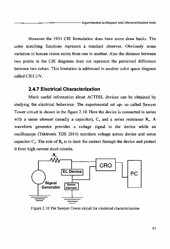
2.4.7 Electrical Characterization
Much useful information about ACTFEL devices can be obtained by
studying the electrical behaviour. The experimental set up- so called Sawyer
Tower circuit is shown in the figure 2.10. Here the device is connected in series
with a sense element (usually a capacitor), Cs and a series resistance Rs. A
waveform generator provides a voltage signal to the device while an
oscilloscope (Tektronix TDS 2014) monitors voltage across device and sense
capacitor Cs. The role of Rs is to limit the current through the device and protect
it from high current short circuits.
R.
eRO PC
Figure 2.10 The Sawyer-Tower circuit for electrical characterization
97

Chaprer2--------------------------------------------________ __
The voltage measured across Cs will give infonnation about total charge
that is transferred across the device. Nonnally Cs is chosen to be very large so
that most of the applied voltage is dropped across the device itself.
150
100
- 50 > -Cl) 0 en J9 O..so >
·100
·150
-200.0", 0.0 200.0", 400.0... 600.0J.! 800.0 ...
time (seconds)
Figure 2.11 Wave fonn used in the present study
Most researchers employ a sine wave or bipolar trapezoidal waveform to
characterize ACTFEL device. In this study we have used bipolar trapezoidal
waveform (Digilog Instruments Pvt, Bangalore). The shape of the wave fonn is
as shown in the figure 2.11.
The rise time Crr) is 30lls, stay (ts) and trail (tt) time is 70 IlS which was
quite large when compared to standard values (tr =5Ils-,ts = 30 j..lS and tt =5 j..ls).
98

-------------'--Experimenta/ techniques andpharacterization tools·
External Charge-Voltage characterization
The measurement external charge versus voltage is a standard electrical
characterization technique. The charge on the external terminals of the ACTFEL
device is plotted against applied voltage to the device forming a hysteretic loop.
This external charge is measured using the sense capacitor using the relation qext
= Vs * Cs. This charge is normalized to the area of the device. A Q-V plot is
always hysteretic when dissipative charge conduction in an ACTFEL device is
occurring and hence it is a straight line with slope equal to Ct when an ACTFEL
device is driven below threshold. Therefore the threshold voltage of an ACTFEL
device is the voltage at which the Q-V curve initially becomes hysteretic.
A Q-V plot of a typical ZnS:Mn device is shown in figure 2.12 to
illustrate some of the information that is available from a Q-V plot [31]. The
voltage labeled Vto in figure is termed the negative turn-on voltage whereas the
analogous voltage during the positive portion of the waveform is known as the
positive turn-on voltage Vto• A distinction is made between these two voltages
because they are not in general of equal magnitude although they are normally
very close to the same magnitude The turn on voltage differs from the threshold
voltage due to the polarization charge Qe pol in figure 2.12. Polarization charge is
a measure of the charge imbalance across the phosphor layer of an ACTFEL
device following the conclusion of an applied voltage pulse.
The e superscript indicates that polarization charge as measured in a Q
V plot is a purely external quantity that must be transformed by Eq to give a
measure of the internal phosphor polarization. The polarization charge existing
after the conclusion of a pulse always aids the following pulse of opposite
99

Chaprer2------------------------------------------------------
polarity because both result in electric fields of the same polarity. In fact the
threshold voltage V'h may be defined as
(2.26)
One of the factors that can significantly reduce polarization charge, is
the amount of leakage charge denoted Qe1eak in figure. The leakage charge is a
measure of the amount of charge movement that takes place due to polarization
fields during the inter-pulse intervals segments EF and lA in figure 2.12. The
leakage charge as measured by a Q-V is also a purely external quantity as
denoted by the e superscript and must also be transformed via Eq to get a
measure of actual charge movement through the phosphor layer.
The remaining charge terms in figure 2.12 are the charge terms that
relates to the on time of the ACTFEL device. First the conduction charge labeled
Qcond in figure 2.12 is the amount of charge conducted through the phosphor
layer of the device from device turn-on until the falling edge of the pulse
segments BD and GI in the figure 2.12. The conduction charge as measured by
the Q-V directly corresponds to the internal phosphor conduction charge so no e
superscript is necessary. Next the term Qrelax is termed the relaxation charge and
this is a measure of the charge that flows during the portion of the waveform
where the applied voltage is constant at its maximum value segments CD and HI
in figure 2.12. This charge is termed relaxation charge because the flow of this
charge gives rise to a field opposite to the applied phosphor field and since the
applied voltage is no longer slewing the magnitude of the phosphor field tends to
decrease or relax during this portion of the waveform. Finally the charge labeled
Qe max in figure is termed the maximum charge and corresponds to the maximum
lOO

--------------Experimenta/ techniques and characterization tools
voltage measured across the sense capacitor for a given applied voltage. Note
that Qmax is taken with respect to a charge zero reference point the external
charge axis.
_2 N
E u -u 1 ::1. -Cl) m a 04--------r------~~~~--------------~ .c (,) -ca C -1 ... ~ W -2 r ______ Q· ...
1AX
-200 -100 o 100 200
Applied Voltage (V)
Figure 2.12 Typical Q-V diagram of an ACTFEL device
Thus Qmax differs from all of the other Q-V charges since all of the other
charges represent differences in the voltage across the sense capacitor at two
distinct points of the applied voltage waveform. As seen in a later section Qmax is
a useful quantity for performing transferred charge measurements. It should also
be noted that each of the charges discussed above are labeled for only one
polarity of the driving waveform in figure but they exist for both polarities hence
the and superscripts. The Q-V curve is used to assess several important physical
parameters about ACTFEL devices. First below the turn-on voltage of the
iOl

Chaprer2----------------------------------------------------
ACTFEL device it behaves as a simple capacitor with the capacitance given by
the series combination of the insulator and phosphor capacitances. Since the
slope of a Q-V plot is a capacitance the Q-V slope below turn-on region (AB and
FG segments) yields the total device capacitance Ct. Next if the phosphor layer
is assumed to be shorted during the post turn-on portion of the driving waveform
(segments BC and GH in figure 2.12) the slope of the Q-V curve in this region
corresponds to the insulator capacitance of the ACTFEL device Cj. This should
be approached with some caution, however because if there is space charge
generation during this time the slope of the Q-V can become much greater than
the physical insulator capacitance. On the other hand, sometimes the phosphor
layer may be incompletely shunted and the slope of the Q-V may be much less
than the physical insulator capacitance. Finally the area enclosed within a Q-V
curve is equal to the input electrical power density delivered to the ACTFEL
device per pulse.
References
1. J. George, Preparation o/Thin Films, p.l, Marcel Dekker Inc., New York
(1992)
2. T. Sei, Y. Nomura and T. Tsuchiya, J. Non-Cryst. Solids, 218, 135 (1997)
3. Z. Ji, L. Kun, S. Yongliang and Y. Zhizhen, J. Cryst. Growth, 255, 353
(2003)
4. Z. Van, M. Koike and H. Takei, J. Cryst. Growth, 165, 183 (1996)
5. S. H. Yang, J. Electrochem. Soc., 150, H250 (2003)
6. Z. Lou and J. Hao, Appl. Phys. A, 80, 151 (2005)
7. J. Hao, Z. Lou, I. Renaud and M. Cocivera, Thin Solid Films, 467, 182
(2004) 102

-------------Experimental techniques and characterization tools
8. T. Miyata, T. Nakatani and T. Minami, Thin Solid Films, 373, 145 (2000)
9. N. Honda, T. Suzuki, T. Yunogami, H. Suematsu, W. Jiang and K. Yatsui,
Jpn. J. Appl. Phys., 44, 695 (2005)
10. T. Minami, Y. Kuroi and S. Dakata,J. Vac. Sci. Technol. A, 14,1736 (1996)
11. L. I. Maissel and R. Glang, Handbook of Thin Film Technology, p.22,
McGraw-HiIl, New York (1970)
12. L. Holland, Vacuum Deposition of Thin films, p.l 04, John WHey & Sons
Inc., New York, 1956
13. W. D. Gill and E. Kay, Rev. Sci. Instrum. 36, 277 (1965)
14. I. G. Kesaer and V. V. Pashkoba, Sov. Phys. Tech. Phys. 4,254 (1959)
15. S. Hayakawa and K. Wasa,J. Phys. Soc. Jpn. 20,1692 (1965)
16. R. McMahon, J. Affinito, and R. R. Parsons, J. Vac. Sei. Technol. 20, 376
(1982)
17. V. S. Smentkowski, Progress in Swface Science, 64, 1 (2000)
18. R. Venkatesan and S. M. Green; The industrial physicist, 22 (1996)
19. D. B. Chrisey and G. K. Hubler, Pulsed Laser Deposition afThin Films,
p.229, John WHey and sons Inc., New York, 1994
20. T. Minami, T. Nakatani and T. Miyata, J. Vac. Sei. Teehnol. A, 18, 1234
(2000)
21. T. Minami, T. Shirai, T. Nakatani and T. Miyata, Jpn. J. Appl. Phys., 39,
L524 (2000)
22. Veeco Dektak 6M Manual (2004)
23. B.D. CuIlity and S.R. Stock, Elements of X ray diffraction, Third edition,
Prentice Hall, New Jersey (2001)
103

Chapwr2--------------------------------------------------
24. Charles Kittel, Introduction to Solid State Physics, Seventh edition, Wiley
Eastern Limited, New Delhi (1996)
25. D. K. Schroder Semiconductor material and device characterization, second
edition, p.651, John Wiley & Sons Inc., New York (1998)
26. P. E .J. Flewit and R. K. Wild, Physical methodsfor material
characterization, Second edition, p.501, lOP publishing, London (2003)
27. P. Kubelka and F. Munk, Zh. Tekh. Fiz., 12, 593 (1931)
28. P. Kubelka, J. Opt. Sac .Am., 38, 448 (1948)
29. D. R.Vij (Ed.) Luminescence of solids, p.46, Plenum Press, New York
(1998)
30. P. A. Keller, Information Display, 12, 36 ( 1996)
31. P. D. Keir and J. F. Wager, Ann. Rev. Mater. Sci., 27,223 (1999)
104