Synchronous Sequential Logic -...
94
Synchronous Sequential Logic EE 200 Digital Logic Circuit Design Dr. Abdulaziz Tabbakh College of Computer Sciences and Engineering King Fahd University of Petroleum and Minerals
Transcript of Synchronous Sequential Logic -...

Synchronous Sequential Logic
EE 200
Digital Logic Circuit Design
Dr. Abdulaziz Tabbakh
College of Computer Sciences and Engineering
King Fahd University of Petroleum and Minerals

EE 200– Digital Logic Circuit Design – KFUPM slide 2
Outline
Introduction
Sequential Circuits
Storage Elements:
Latches
Flip‐Flops
Characteristic Tables
Analysis of Clocked Sequential Circuits
State Reduction and Assignment
Flip-flop Excitation Tables
Design Procedure
Synthesis using different flip flops

EE 200– Digital Logic Circuit Design – KFUPM slide 3
Introduction
Logic Circuits
Combinational Sequential
A sequential circuit consists of a combinational circuit to which
storage elements are connected to form a feedback path.
The binary information stored in the memory elements define
the current state of the sequential circuit.
A sequential circuit receives information from an external
input as well as the present state of the memory elements to
determine the output and next state.
EE 200– Digital Logic Circuit Design – KFUPM slide 4
Sequential Logic Circuits
A sequential circuit is specified by a time sequence of
inputs, outputs, and internal states.
Two main types of sequential circuits based on the
timing of their signals :
Synchronous sequential circuits are systems whose behavior can be defined from the knowledge of its signals at discreteinstants of time.
Asynchronous circuits are systems whose behavior depends upon the input signals at any time instant and the order in which the inputs change. So it is a combinational system with feedback.

EE 200– Digital Logic Circuit Design – KFUPM slide 5
Sequential Logic Circuits
Synchronous Sequential Circuit
Uses a clock signal as an additional input
Changes in the memory elements are controlled by the clock
Changes happen at discrete instances of time
Asynchronous Sequential Circuit
No clock signal
Changes in the memory elements can happen at any instance
of time
Our focus will be on Synchronous Sequential Circuits
Easier to design and analyze than asynchronous sequential
circuits

EE 200– Digital Logic Circuit Design – KFUPM slide 6
Synchronous Sequential Circuits
Synchronous sequential circuits use a clock signal
The clock signal is an input to the memory elements
The clock determines when the memory should be
updated
The present state = output value of memory (stored)
The next state = input value to memory (not stored yet)

EE 200– Digital Logic Circuit Design – KFUPM slide 7
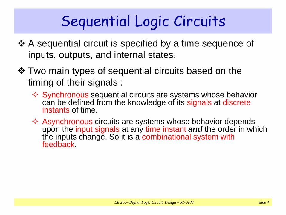
Clock (CLK)
Clock generator provides a clock signal having the form
of a periodic train of clock pulses.
The clock determine when computational activity will
occur in the circuit (transition from 0 1, or 10)
The other signals (inputs and current state) determine
what changes will take place affecting the storage
elements and the outputs.
Synchronous sequential circuits that use clock pulses to
control storage elements are called clocked sequential
circuits.
EE 200– Digital Logic Circuit Design – KFUPM slide 8
Clock (CLK)
Tpos = Time of the positive portion of the clock
T = Duration of a complete cycle.
Tpos/T = Duty Cycle.
50% duty cycle divides the clock period into half positive and half zero (negative).
The frequency of the clock is found by: F=1/T.
Example, if the clock period is 1ns then the frequency of the clock is 1GHz.
TTpos
EE 200– Digital Logic Circuit Design – KFUPM slide 9
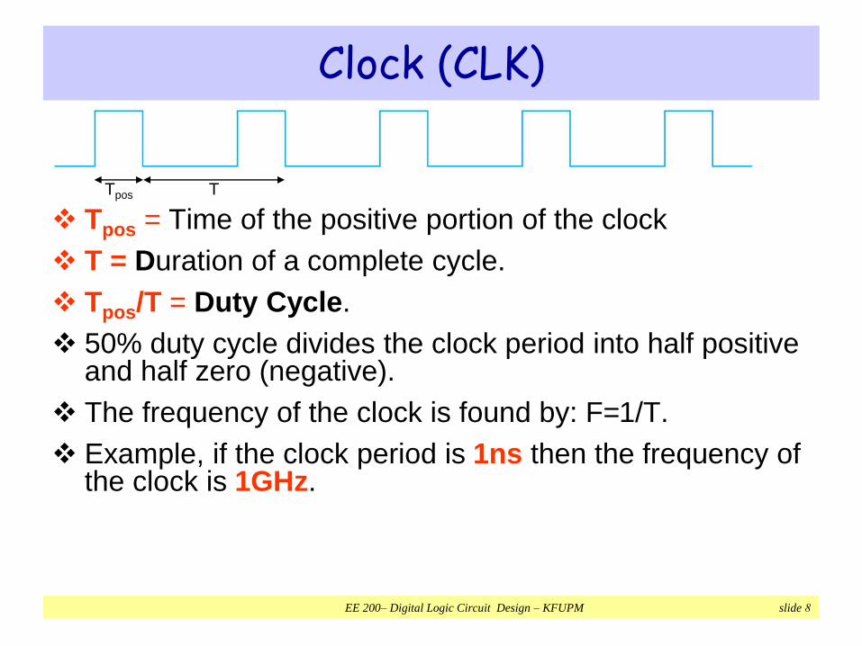
Clock (CLK)
Clock is a periodic signal = Train of pulses (1's and 0's)
The same clock cycle repeats indefinitely over time
Positive Pulse: when the level of the clock is 1
Negative Pulse: when the level of the clock is 0
Rising Edge (Positive Edge): when the clock goes from 0
to 1
Falling Edge (Negative Edge): when the clock goes from 1
down to 0
Time
Clock
cycle
Clock
cycle
Positiv
e
Pulse
Negative
Pulse

EE 200– Digital Logic Circuit Design – KFUPM slide 10
Memory Elements
They are called flip-flops (FFs)
A flip-flop is a binary storage device capable of storing
one bit of information.
A sequential circuit may use many flip-flops to store as
many bits as necessary
A change in state of the flip-flops is initiated only by a
clock pulse transition.
EE 200– Digital Logic Circuit Design – KFUPM slide 11
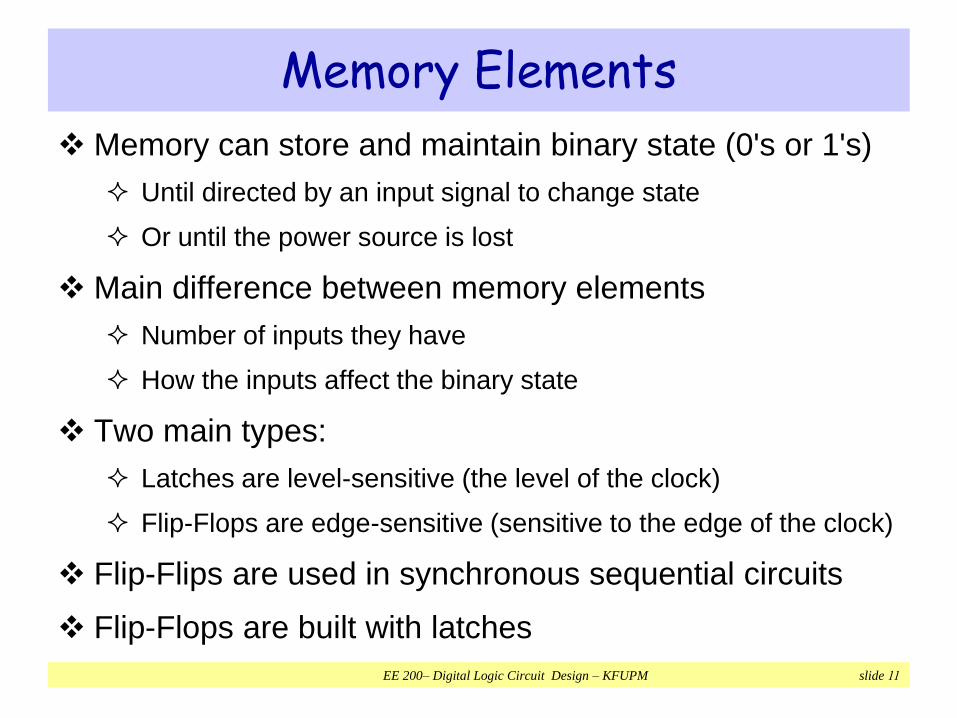
Memory Elements
Memory can store and maintain binary state (0's or 1's)
Until directed by an input signal to change state
Or until the power source is lost
Main difference between memory elements
Number of inputs they have
How the inputs affect the binary state
Two main types:
Latches are level-sensitive (the level of the clock)
Flip-Flops are edge-sensitive (sensitive to the edge of the clock)
Flip-Flips are used in synchronous sequential circuits
Flip-Flops are built with latches

EE 200– Digital Logic Circuit Design – KFUPM slide 12
SR Latch
A latch is binary storage element that can store 0 or 1
It is the most basic memory element
An SR Latch can be built using two NOR gates
Two inputs: 𝑆 (Set) and 𝑅 (Reset)
Two outputs: 𝑄 and 𝑄
EE 200– Digital Logic Circuit Design – KFUPM slide 13
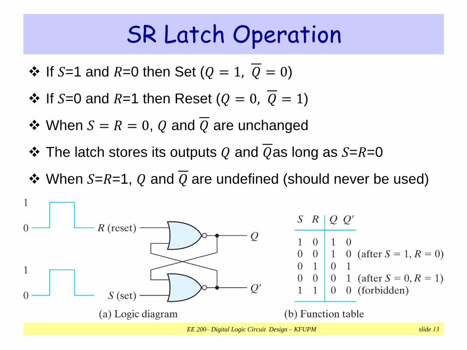
SR Latch Operation
If 𝑆=1 and 𝑅=0 then Set (𝑄 = 1, 𝑄 = 0)
If 𝑆=0 and 𝑅=1 then Reset (𝑄 = 0, 𝑄 = 1)
When 𝑆 = 𝑅 = 0, 𝑄 and 𝑄 are unchanged
The latch stores its outputs 𝑄 and 𝑄as long as 𝑆=𝑅=0
When 𝑆=𝑅=1, 𝑄 and 𝑄 are undefined (should never be used)
EE 200– Digital Logic Circuit Design – KFUPM slide 14
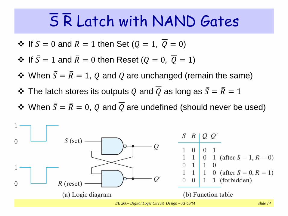
S R Latch with NAND Gates
If ҧ𝑆 = 0 and ത𝑅 = 1 then Set (𝑄 = 1, 𝑄 = 0)
If ҧ𝑆 = 1 and ത𝑅 = 0 then Reset (𝑄 = 0, 𝑄 = 1)
When ҧ𝑆 = ത𝑅 = 1, 𝑄 and 𝑄 are unchanged (remain the same)
The latch stores its outputs 𝑄 and 𝑄 as long as ҧ𝑆 = ത𝑅 = 1
When ҧ𝑆 = ത𝑅 = 0, 𝑄 and 𝑄 are undefined (should never be used)

EE 200– Digital Logic Circuit Design – KFUPM slide 15
SR Latch with a Enable Input
An additional Enable input signal En is used
Enable controls when the state of the latch can be changed
When En=0, the S and R inputs have no effect on the latch
The latch will remain in the same state, regardless of S and R
When En=1, then normal SR latch operation

EE 200– Digital Logic Circuit Design – KFUPM slide 16
D Latch (Transparent Latch) with Enable Input
Only one data input 𝐷
An inverter is added: 𝑆=𝐷 and 𝑅 = ഥ𝐷
𝑆 and 𝑅 can never be 11 simultaneously No
undefined state
When En=0, 𝑄 remains the same (No change in state)
When En=1, 𝑄=𝐷 and ത𝑄 = ഥ𝐷

EE 200– Digital Logic Circuit Design – KFUPM slide 17
Graphic Symbols for Latches
A bubble appears at the complemented output 𝑄
Indicates that 𝑄 is the complement of 𝑄
A bubble also appears at the inputs of an 𝑆 𝑅 latch
Indicates that logic-0 is used (not logic-1) to set (or
reset) the latch (as in the NAND latch implementation)

EE 200– Digital Logic Circuit Design – KFUPM slide 18
Problem with Latches
A latch is level-sensitive (sensitive to the level of the En)
As long as the enable signal (control) is high …
Any change in the value of input 𝐷 appears in the output 𝑄
Output 𝑄 keeps changing its value as long as the enable is
activated
Final value of output 𝑄 is uncertain
𝐷
𝐸𝑛
𝑄
𝑄
𝐷
𝐿𝑎𝑡𝑐ℎ
𝑋 = 1
Due to this uncertainty,
latches are NOT used
as memory elements in
synchronous circuits
EE 200– Digital Logic Circuit Design – KFUPM slide 19
Problem with Latches
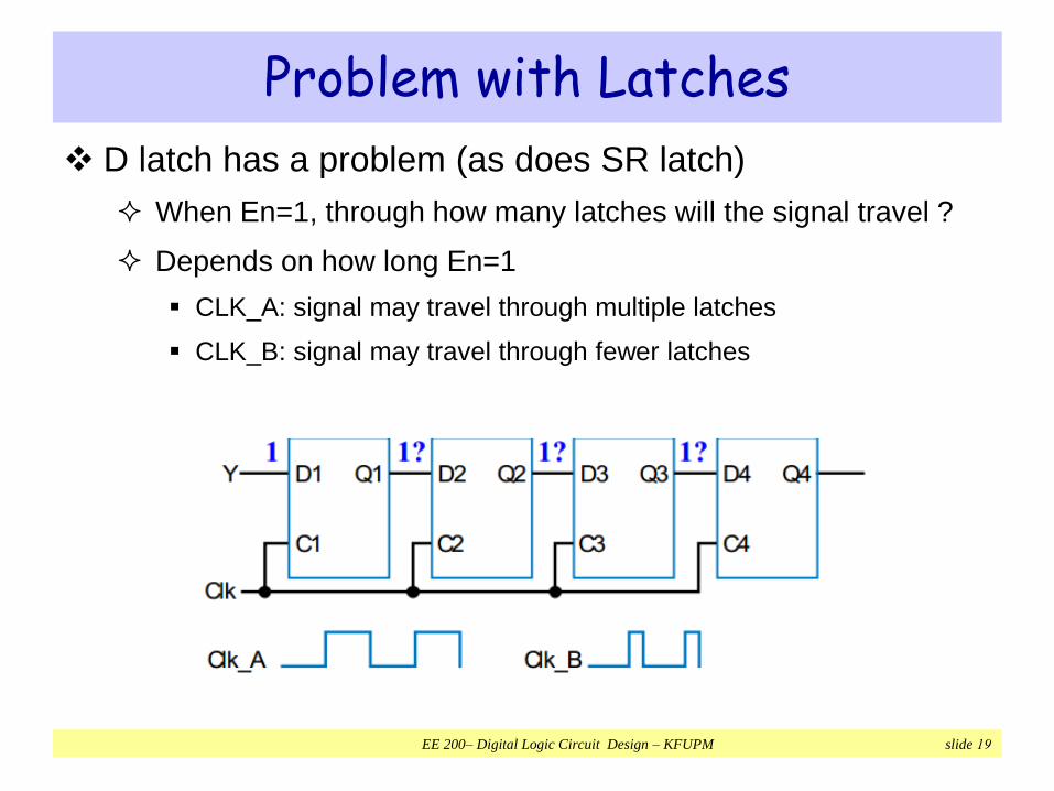
D latch has a problem (as does SR latch)
When En=1, through how many latches will the signal travel ?
Depends on how long En=1
CLK_A: signal may travel through multiple latches
CLK_B: signal may travel through fewer latches

EE 200– Digital Logic Circuit Design – KFUPM slide 20
Flip-Flops
A Flip-Flop is a better memory element for synchronous
circuits
Solves the problem of latches in synchronous sequential
circuits
A latch is sensitive to the level of the clock
However, a flip-flop is sensitive to the edge of the clock
A flip-flop is called an edge-triggered memory element
It changes it output value at the edge of the clock
Time
Rising edge
Falling edge
Rising edge
Falling edge
HighLevel
LowLevel
EE 200– Digital Logic Circuit Design – KFUPM slide 21
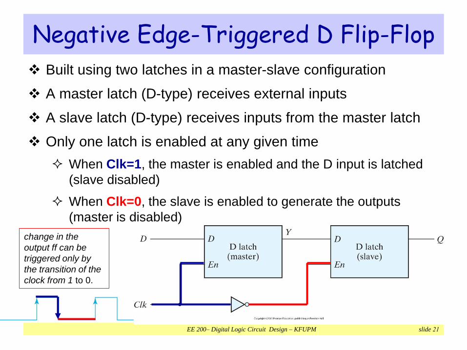
Negative Edge-Triggered D Flip-Flop
Built using two latches in a master-slave configuration
A master latch (D-type) receives external inputs
A slave latch (D-type) receives inputs from the master latch
Only one latch is enabled at any given time
When Clk=1, the master is enabled and the D input is latched
(slave disabled)
When Clk=0, the slave is enabled to generate the outputs
(master is disabled)
change in the
output ff can be
triggered only by
the transition of the
clock from 1 to 0.

EE 200– Digital Logic Circuit Design – KFUPM slide 22
Master-Slave FF
The behavior of the master–slave flip-flop just described
dictates that
The output may change only once
A change in the output is triggered by the edge of the clock
The change may occur only during the clock’s negative level.
The value that is produced at the output of the flip-flop is
the value that was stored in the master stage
immediately before the negative edge occurred.
It is also possible to design a positive edge-triggered
FF.

EE 200– Digital Logic Circuit Design – KFUPM slide 23
D-FF using 3 SR Latches
Two latches respond to D and
Clk. The third latch provides the
outputs for the ff.
Clk=0 S=R=1 Q(t+1)=Q(t)
Clk=1 & D=0 Q=0
If D changes while CLK = 1, R
remains at 0 because Q=0 and the
output is not changed!

EE 200– Digital Logic Circuit Design – KFUPM slide 24
Positive Edge Triggered D-FF
Two of the three SR latches
responds to CLK and D inputs,
the third provides output.
CLK=0 Q(t+1)=Q(t)
CLK=1 & D=0 Q=0
CLK=1 & D=1 Q=1
If D changes while CLK = 1,
R remains at 0 because Q=0
and the output is not changed!
Thus, the flip-flop is locked out
and is unresponsive to further
changes in the input
Output Changes only on CLK
transition from 01, and no
other change!
0
0
1
1
NC
0
1
1
0
1
1
1 0
0

EE 200– Digital Logic Circuit Design – KFUPM slide 25
D-Flip Flops
In a positive edge triggered FF, output changes on CLK transition from
01
In a negative edge triggered FF, output changes on CLK transition from
10
It is similar to the symbol used for the D latch
The arrowhead symbol in front of the Clk, designating a dynamic input
The dynamic indicator (>) indicates sensitivity to the edge of the clock.
A bubble at the C input indicates negative edge-triggered FF

EE 200– Digital Logic Circuit Design – KFUPM slide 26
Flip-Flop Timing
Setup Time (Ts): There is a minimum time during which
the D must be valid and stable before the clock edge.
Hold Time (Th): there is a minimum time during which D
must not change after the clock edge.
Propagation Delay: the interval between the trigger edge
and the stabilization of the output to a new state
CLK
D
Q

EE 200– Digital Logic Circuit Design – KFUPM slide 27
Other Flip-Flops
The most economical and efficient FF is D-FF because it
requires the least number of gates.
Other types of FF can be constructed using the D-FF
and external logic
Two less widely used flip-flops are JK-FF and T-FF

EE 200– Digital Logic Circuit Design – KFUPM slide 28
JK Flip-Flop
The JK is another type of Flip-Flop with inputs: J, K, and Clk
When JK = 10 Set, When JK = 01 Reset
When JK = 00 No change, When JK = 11 Invert outputs
JK can be implemented using two Clocked SR latches and
gates

EE 200– Digital Logic Circuit Design – KFUPM slide 29
T (Toggle) Flip-Flop
The T (Toggle) flip-flop has inputs: T and Clk
When T = 0 No change, When T = 1 Invert outputs
The T flip-flop can be implemented using a JK flip-flop
It can also be implemented using a D flip-flop and a XOR
gate
T-FF is useful for designing binary counters.

EE 200– Digital Logic Circuit Design – KFUPM slide 30
Flip-Flop Characteristic Tables
Defines the operation of a flip-flop in a tabular form
Next state is defined in terms of the current state and the
inputs
𝑄(𝑡) refers to current state before the clock edge arrives
𝑄(𝑡+1) refers to next state after the clock edge arrives
EE 200– Digital Logic Circuit Design – KFUPM slide 31
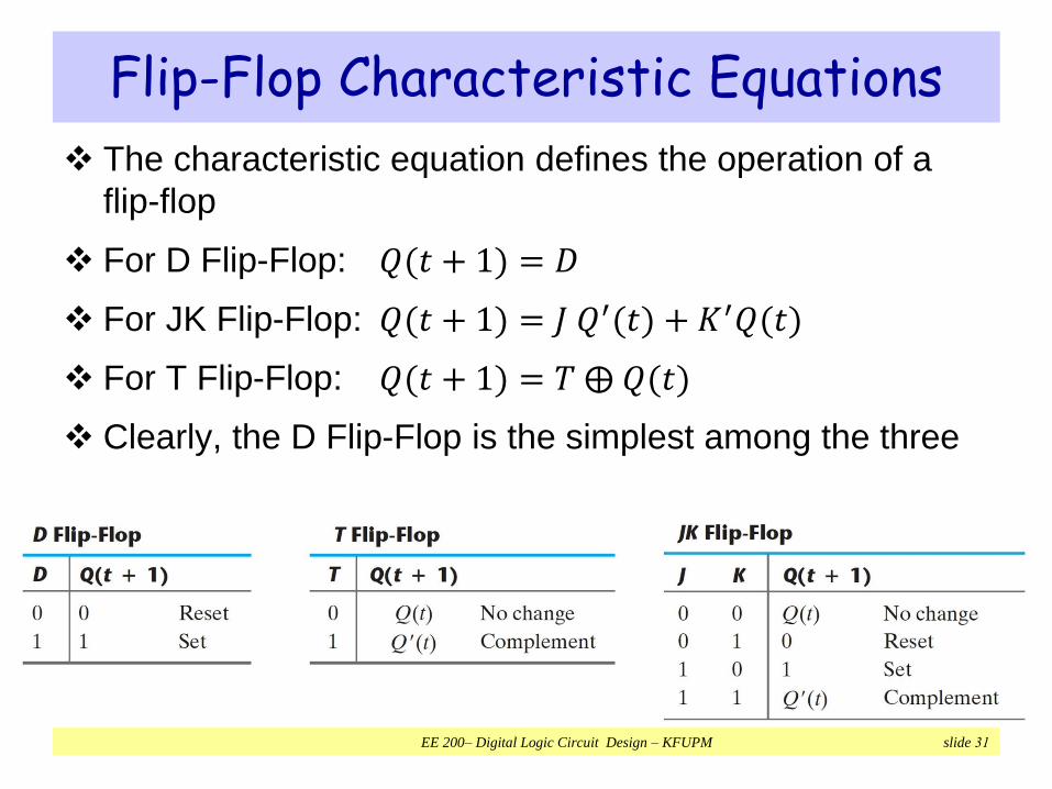
Flip-Flop Characteristic Equations
The characteristic equation defines the operation of a
flip-flop
For D Flip-Flop: 𝑄(𝑡 + 1) = 𝐷
For JK Flip-Flop: 𝑄(𝑡 + 1) = 𝐽 𝑄′(𝑡) + 𝐾′𝑄(𝑡)
For T Flip-Flop: 𝑄(𝑡 + 1) = 𝑇 ⨁ 𝑄(𝑡)
Clearly, the D Flip-Flop is the simplest among the three
EE 200– Digital Logic Circuit Design – KFUPM slide 32
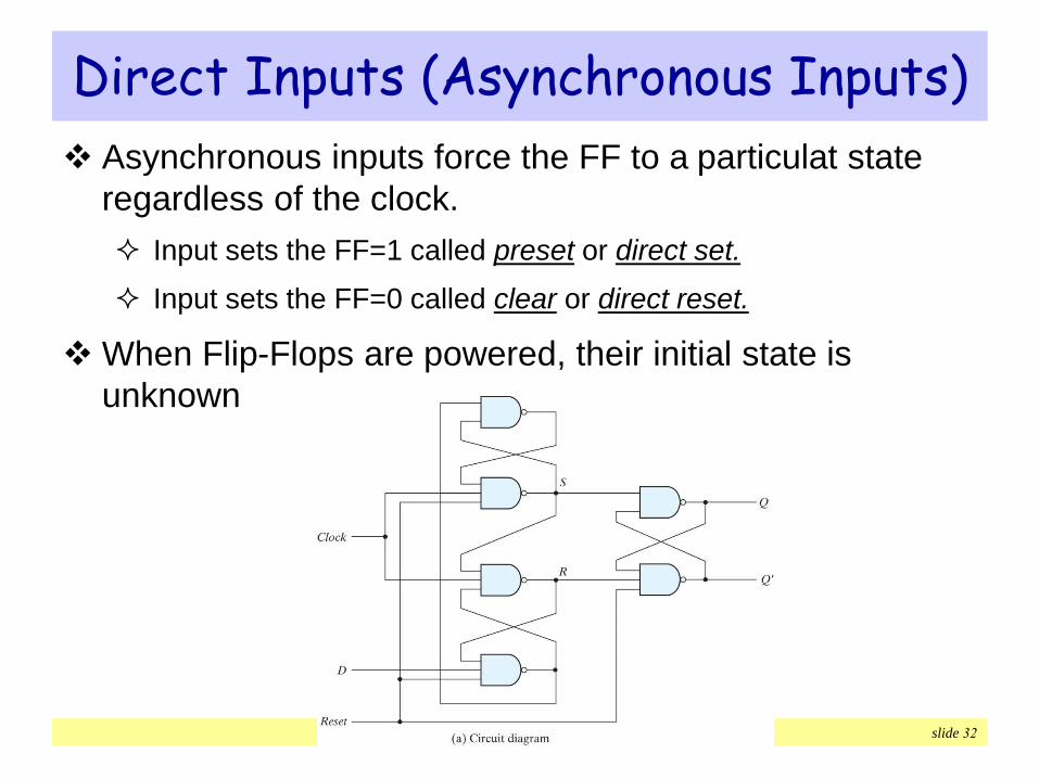
Direct Inputs (Asynchronous Inputs)
Asynchronous inputs force the FF to a particulat state
regardless of the clock.
Input sets the FF=1 called preset or direct set.
Input sets the FF=0 called clear or direct reset.
When Flip-Flops are powered, their initial state is
unknown

EE 200– Digital Logic Circuit Design – KFUPM slide 33
D-FF with Asynchronous Reset When R = 0, the output is
reset to 0, regardless of
the values of D and Clk.
0
1
1

EE 200– Digital Logic Circuit Design – KFUPM slide 34
Analysis of Clocked Sequential Circuits Analysis is describing what a given circuit will do
The behavior of a clocked sequential circuit is determined from the
inputs, the outputs, and the state of its flip-flops.
The outputs and the next state are both a function of the inputs
and the present state.
Analysis Procedure:
obtaining a state table or a state diagram for the time sequence of
inputs, outputs, and internal states.
write Boolean expressions that describe the behavior of the sequential
circuit (state equations).
A state equation describes the next state as a function of the
present state and inputs.
A logic diagram is recognized as a clocked sequential circuit if it
includes flip-flops with clock input
EE 200– Digital Logic Circuit Design – KFUPM slide 35
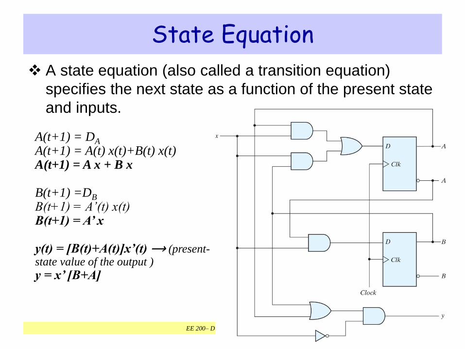
State Equation
A state equation (also called a transition equation)
specifies the next state as a function of the present state
and inputs.
A(t+1) = DA
A(t+1) = A(t) x(t)+B(t) x(t)A(t+1) = A x + B x
B(t+1) =DB
B(t+1) = A’(t) x(t)B(t+1) = A’ x
y(t) = [B(t)+A(t)]x’(t) ⟶ (present-state value of the output )
y = x’ [B+A]

EE 200– Digital Logic Circuit Design – KFUPM slide 36
State Table
State table shows the Next State and Output in a tabular
form
Next State Equations: 𝑨(𝒕+𝟏)=𝑨𝒙+𝑩𝒙 and 𝑩(𝒕+𝟏)=𝑨′𝒙
Output Equation: 𝒚=(𝑨+𝑩)𝒙′
Another form of the state table

EE 200– Digital Logic Circuit Design – KFUPM slide 37
State Table
A sequential circuit with m flipflops and n inputs needs
2m +n rows in the state table.
The next-state section m columns, one for each flip-flop.
The output section has as many columns as there are
output variables.

EE 200– Digital Logic Circuit Design – KFUPM slide 38
State Diagram
State diagram is a graphical representation of a state table
The circles are the states
Two state variable Four states (ALL values of 𝑨 and 𝑩)
Arcs are the state transitions
Labeled with: Input 𝒙 / Output 𝒚
EE 200– Digital Logic Circuit Design – KFUPM slide 39
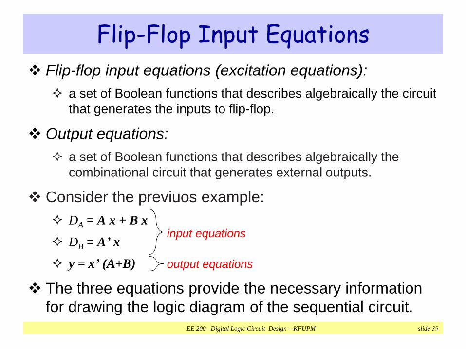
Flip-Flop Input Equations
Flip-flop input equations (excitation equations):
a set of Boolean functions that describes algebraically the circuit
that generates the inputs to flip-flop.
Output equations:
a set of Boolean functions that describes algebraically the
combinational circuit that generates external outputs.
Consider the previuos example:
DA = A x + B x
DB = A’ x
y = x’ (A+B)
The three equations provide the necessary information
for drawing the logic diagram of the sequential circuit.
input equations
output equations
EE 200– Digital Logic Circuit Design – KFUPM slide 40
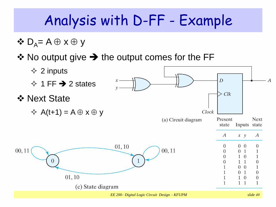
Analysis with D-FF - Example
DA= A x y
No output give the output comes for the FF
2 inputs
1 FF 2 states
Next State
A(t+1) = A x y

EE 200– Digital Logic Circuit Design – KFUPM slide 41
Analysis with JK-FF
When a flip-flop other than the D type is used, such as
JK or T, it is necessary to refer to the corresponding
characteristic table or characteristic equation to obtain
the nextstate values.
Next-State Values for Sequential circuits using JK-FF or
T-FF can be found as follows:
Determine FF input equations
List binary inputs for each input equation
Use corresponding FF characteristic table to predict next state
EE 200– Digital Logic Circuit Design – KFUPM slide 42
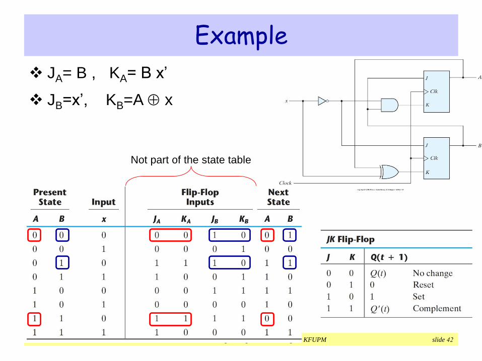
Example
JA= B , KA= B x’
JB=x’, KB=A x
Not part of the state table

EE 200– Digital Logic Circuit Design – KFUPM slide 43
Analysis with JK-FF
The next-state values can also be obtained by
evaluating the state equations from the characteristic
equation. This is done as:
1. Determine the FF input equations
2. Substitute the input equations into the FF characteristic
equation to get the state equations
3. Use corresponding state equations to determine next state
values in the state table.

EE 200– Digital Logic Circuit Design – KFUPM slide 44
Example
A(t + 1) = JAA’ + K’AA B(t + 1) = JBB’ + K’BB
JA= B , KA= B x’ JB=x’, KB=A x
A(t + 1) = BA + (Bx’)’ A = A’B + AB’ + Ax
B(t + 1) = x’B’ + (A x)’B = B’x’ + ABx + A’Bx’state equations

EE 200– Digital Logic Circuit Design – KFUPM slide 45
Analysis with T-FF - Example
Charactristic equation
𝑄 𝑡 + 1 = 𝑇 ⊕𝑄 = 𝑇′𝑄 + 𝑇𝑄′
TA = xB A(t+1) = (xB)’A + xBA’ = x’A + AB’ + xA’B
TB = x B(t+1) = x’B + xB’
y = AB

EE 200– Digital Logic Circuit Design – KFUPM slide 46
Analysis with T-FF - Example
The circuit behaves as a binary counter with a sequence of
states 00, 01, 10, 11, and back to 00 as long as input x is
equal to 1. The output y=1 when the counter reaches 11
the output depends on the present state only and is
independent of the input
EE 200– Digital Logic Circuit Design – KFUPM slide 47
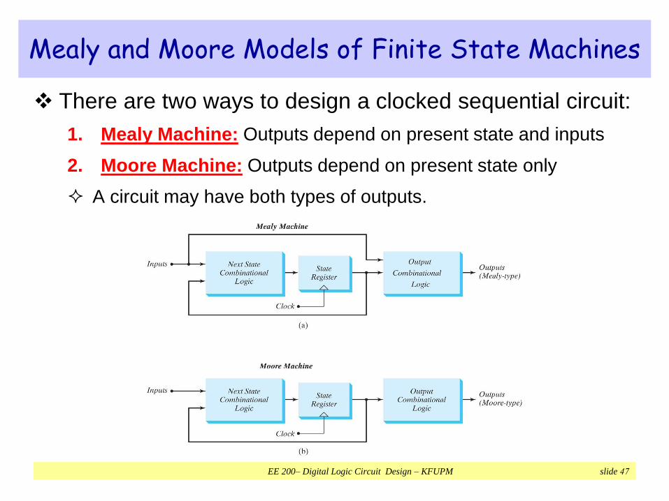
Mealy and Moore Models of Finite State Machines
There are two ways to design a clocked sequential circuit:
1. Mealy Machine: Outputs depend on present state and inputs
2. Moore Machine: Outputs depend on present state only
A circuit may have both types of outputs.

EE 200– Digital Logic Circuit Design – KFUPM slide 48
Mealy Machine (Mealy FSM)
The outputs are a function of the present state and Inputs
The outputs are NOT synchronized with the clock
The outputs may change if inputs change during the clock cycle
The outputs may have momentary false values (called glitches)
The correct outputs are present just before the edge of the
clock.

EE 200– Digital Logic Circuit Design – KFUPM slide 49
Mealy FSM
An example of a Mealy state
diagram is shown on the right
Each arc is labeled with:
Input / Output
The output is shown on the
arcs of the state diagram
The inputs are changed at
the inactive edge of the clock
to ensure that the inputs to
the flip-flops stabilize before
the active edge of the clock
occurs.

EE 200– Digital Logic Circuit Design – KFUPM slide 50
Tracing a Mealy State Diagram
Cycle 0 1 2 3 4 5 6 7 8
Input x 0 1 1 0 1 1 1 1 0
PresentState A B
? 0 0 1 0 0 1 1 1
? 0 1 0 0 1 0 0 0
Output z 0 0 0 0 0 0 1 1 0
When the circuit is powered, the initial state (AB) is unknown
Even though the initial state is unknown, the input x = 0 forces
a transition to state AB = 00, regardless of the present state
Sometimes, a reset input is used to initialize the state to 00

EE 200– Digital Logic Circuit Design – KFUPM slide 51
False Output in the Timing Diagram
Cycle 0 1 2 3 4 5 6 7 8
Input x 0 1 1 0 1 1 1 1 0
PresentState A B
? 0 0 1 0 0 1 1 1
? 0 1 0 0 1 0 0 0
Output z 0 0 0 0 0 0 1 1 0
A
B
Negative edge-triggered

EE 200– Digital Logic Circuit Design – KFUPM slide 52
Moore Machine
The outputs are a function of the Flip-Flop outputs only
The outputs depend on the current state only
The outputs are synchronized with the clock
Glitches cannot appear in the outputs (even if inputs change)
A given design might mix between Mealy and Moore

EE 200– Digital Logic Circuit Design – KFUPM slide 53
Moore State Diagram
An example of a Moore state
diagram is shown on the right
Arcs are labeled with input only
The output is shown inside the
state: (State / Output)
The output depends on the
current state only
00
0
01
0
10
0
11
1
1
1
1
0 0
0
1
0

EE 200– Digital Logic Circuit Design – KFUPM slide 54
Tracing a Moore State Diagram
When the circuit is powered, the initial
state (AB) and output are unknown
Input x = 0 resets the state AB to 00.
Can also be done with a reset signal.
Cycle 0 1 2 3 4 5 6 7 8
Input x 0 1 1 0 1 1 1 1 0
PresentState A B
? 0 0 1 0 0 1 1 1
? 0 1 0 0 1 0 1 1
Output z ? 0 0 0 0 0 0 1 1
00
0
01
0
10
0
11
1
1
1
1
0 0
0
1
0

EE 200– Digital Logic Circuit Design – KFUPM slide 55
Timing Diagram of a Moore MachineCycle 0 1 2 3 4 5 6 7 8
Input x 0 1 1 0 1 1 1 1 0
PresentState A B
? 0 0 1 0 0 1 1 1
? 0 1 0 0 1 0 1 1
Output z ? 0 0 0 0 0 0 1 1
Negative edge-triggered
A
B
The output is
synchronized with the
clock. No false output
(or glitch) can appear.
EE 200– Digital Logic Circuit Design – KFUPM slide 56
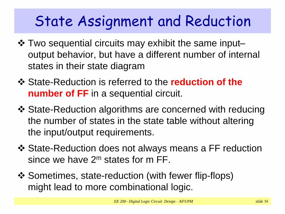
State Assignment and Reduction
Two sequential circuits may exhibit the same input–
output behavior, but have a different number of internal
states in their state diagram
State-Reduction is referred to the reduction of the
number of FF in a sequential circuit.
State-Reduction algorithms are concerned with reducing
the number of states in the state table without altering
the input/output requirements.
State-Reduction does not always means a FF reduction
since we have 2m states for m FF.
Sometimes, state-reduction (with fewer flip-flops)
might lead to more combinational logic.

EE 200– Digital Logic Circuit Design – KFUPM slide 57
Example
Only input-output sequences are
important, the internal states are
used to provide required
sequences.
There are an infinite number of
input sequences that may be
applied to the circuit; each results
in a unique output sequence.

EE 200– Digital Logic Circuit Design – KFUPM slide 58
Example
Consider the input sequence:
01010110100 starting from the
initial state a
In this circuit the states
themselves are of secondary
importance, because we are
interested only in output sequences
caused by input sequences.
The output will follow:
State a a b c d e f f g f g a
Input 0 1 0 1 0 1 1 0 1 0 0
Output 0 0 0 0 0 1 1 0 1 0 0

EE 200– Digital Logic Circuit Design – KFUPM slide 59
State Reduction
Two circuits are said to be identical if the same applied
input sequence gives the same output sequence.
The challenge with state-reduction is to find ways to
reduce the number of states without affecting the input-
output relationships.
“Two states are said to be equivalent, if, for each set of
inputs, they give exactly the same output and send the
circuit to the same state or to an equivalent state.”
When two states are equivalent, one of them can be
removed without altering the input–output relationships.

EE 200– Digital Logic Circuit Design – KFUPM slide 60
Example – Contd.
e and g are equivalent!
Remove row with g, and replace g with e whenever it occurs as next
State!

EE 200– Digital Logic Circuit Design – KFUPM slide 61
Example – Contd.
d and f are equivalent!
Remove row with f, and replace f with d whenever it occurs as next
State!

EE 200– Digital Logic Circuit Design – KFUPM slide 62
Example – Contd.
We have reduced number of states from 7 to 5!
We did not save a FF in this design, but we have more un-used states
that we can substitute for as don’t cares during design, thus simplifying
some combinational design logic.

EE 200– Digital Logic Circuit Design – KFUPM slide 63
Verify Reduction
State a a b c d e f f g f g a
Input 0 1 0 1 0 1 1 0 1 0 0
Output 0 0 0 0 0 1 1 0 1 0 0
State a a b c d e d d e d e a
Input 0 1 0 1 0 1 1 0 1 0 0
Output 0 0 0 0 0 1 1 0 1 0 0

EE 200– Digital Logic Circuit Design – KFUPM slide 64
State Assignment
it is necessary to assign unique coded binary values to
the states.
For a circuit with m states, the codes must contain at
least n bits, where 2n ≥ m
One-hot encoding usually leads to simpler logic for the
next state and output.

EE 200– Digital Logic Circuit Design – KFUPM slide 65
State Assignment
A different assignment will result in a state table with
different binary values for the states.
The complexity of the combinational circuit depends on
the binary state assignment chosen.
Transition table is used for a state table with a binary
assignment.
EE 200– Digital Logic Circuit Design – KFUPM slide 66
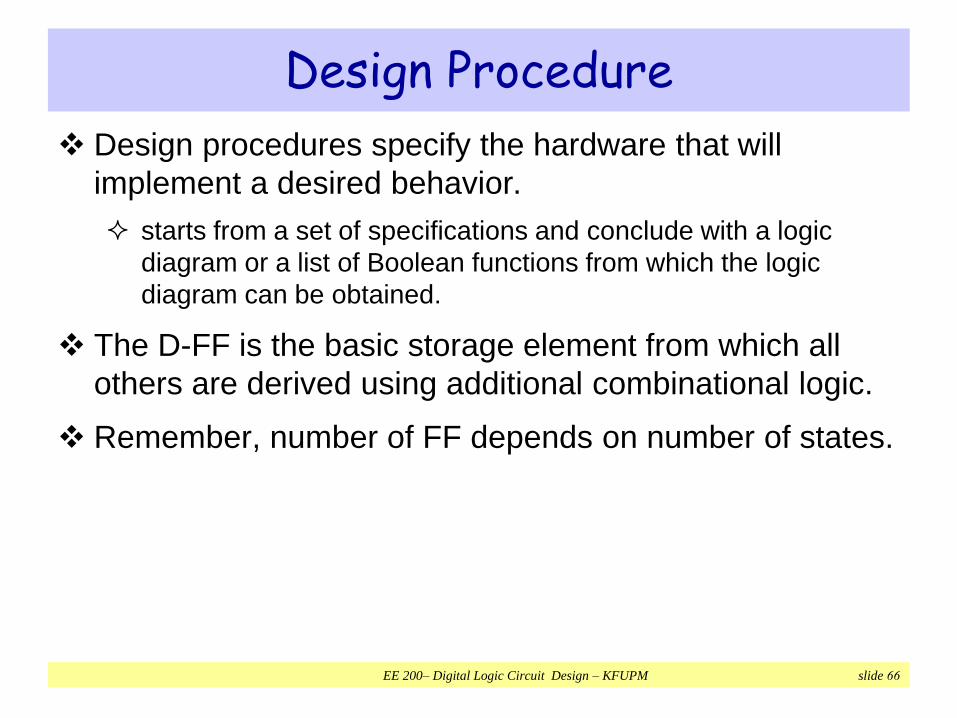
Design Procedure
Design procedures specify the hardware that will
implement a desired behavior.
starts from a set of specifications and conclude with a logic
diagram or a list of Boolean functions from which the logic
diagram can be obtained.
The D-FF is the basic storage element from which all
others are derived using additional combinational logic.
Remember, number of FF depends on number of states.

EE 200– Digital Logic Circuit Design – KFUPM slide 67
Design Procedure
1. Obtain a state table of state diagram for the sequential
circuit
2. Reduce the number of states if necessary
3. Assign binary codes for the states
4. Obtain the binary coded state table
5. Choose the FF type to be used
6. Derive the simplified FF input equations
7. Derive the simplified output equations
8. Draw the Logic Circuit diagram

EE 200– Digital Logic Circuit Design – KFUPM slide 68
Example: Sequence Detector
A sequence detector is a sequential circuit
Detects a specific sequence of bits in the input
The input is a serial bit stream: One input bit 𝒙 is fed to
the sequence detector each cycle
The output is also a bit stream: One output bit 𝒛 each
cycle indicates whether a given sequence is detected or
not
Sequence
Detector
𝒙𝒛
𝑐𝑙𝑘

EE 200– Digital Logic Circuit Design – KFUPM slide 69
S3
1S2
1S1
1
State Diagram for a Sequence Detector
Example: Design a circuit that detects the input sequence
"111"
Begin in an initial state: call it S0
S0 indicates that a 1 is NOT detected yet
As long as the input 𝑥 is 0, remain in the initial state S0
Add a state (call it S1) that detects the first 1 in the input
Add a state (call it S2) that detects the input sequence "11"
Add a state (call it S3) that detects the input sequence "111"
S0
0

EE 200– Digital Logic Circuit Design – KFUPM slide 70
0
Complete the State Diagram
Moore Design: Assign Output to States
The output in S0, S1, and S2 should be 0
The output in S3 should be 1
0 0
S0
0
S1
0
S2
0
S3
1
1
1
1
0
1
Now complete the state diagram:
Add transitions from S1, S2, S3
back to S0 if the input is 0
Add transition from S3 to itself if
the input is 1 to detect sequences
longer than three 1's

EE 200– Digital Logic Circuit Design – KFUPM slide 71
State Assignment
Each state must be assigned a unique binary code
If there are 𝑚 states then
The minimum number of state bits: 𝑛 = 𝑙𝑜𝑔2𝑚
𝑥 is the smallest integer ≥ 𝑥 (ceiling function)
In our example, there are four states: S0, S1, S2, and S3
Therefore, the minimum number of state bits (Flip-Flops) = 2
State assignment: S0 = 00, S1 = 01, S2 = 10 and S3 = 11
If 𝑛 bits are used, the number of unused states = 2𝑛 −𝑚
In our example, there are NO unused states

EE 200– Digital Logic Circuit Design – KFUPM slide 72
From State Diagram to State Table
0
0 0
S0
0
S1
0
S2
0
S3
1
1
1
1
0
1
PresentState
Next State Output𝒛𝒙 = 0 𝒙 = 1
S0 S0 S1 0
S1 S0 S2 0
S2 S0 S3 0
S3 S0 S3 1
PresentState
Next State Output𝒛𝒙 = 0 𝒙 = 1
0 0 0 0 0 1 0
0 1 0 0 1 0 0
1 0 0 0 1 1 0
1 1 0 0 1 1 1
State Assignment
S0 = 00, S1 = 01
S2 = 10, S3 = 11
EE 200– Digital Logic Circuit Design – KFUPM slide 73
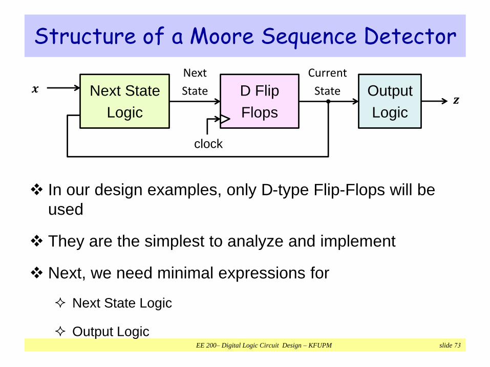
Structure of a Moore Sequence Detector
In our design examples, only D-type Flip-Flops will be
used
They are the simplest to analyze and implement
Next, we need minimal expressions for
Next State Logic
Output Logic
Next State
Logic
𝒙𝒛
D Flip
Flops
Next
State
Current
State Output
Logic
clock
EE 200– Digital Logic Circuit Design – KFUPM slide 74
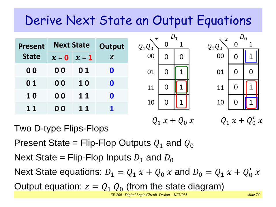
Derive Next State an Output Equations
Two D-type Flips-Flops
Present State = Flip-Flop Outputs 𝑄1 and 𝑄0
Next State = Flip-Flop Inputs 𝐷1 and 𝐷0
Next State equations: 𝐷1 = 𝑄1 𝑥 + 𝑄0 𝑥 and 𝐷0 = 𝑄1 𝑥 + 𝑄0′ 𝑥
Output equation: 𝑧 = 𝑄1 𝑄0 (from the state diagram)
PresentState
Next State Output𝒛𝒙 = 0 𝒙 = 1
0 0 0 0 0 1 0
0 1 0 0 1 0 0
1 0 0 0 1 1 0
1 1 0 0 1 1 1
𝑄1𝑄0𝑥
0 1
00
01
11
10
0 0
0 1
0 1
0 1
𝐷1𝑄1𝑄0
𝑥0 1
00
01
11
10
0 1
0 0
0 1
0 1
𝐷0
𝑄1 𝑥 + 𝑄0 𝑥 𝑄1 𝑥 + 𝑄0′ 𝑥

EE 200– Digital Logic Circuit Design – KFUPM slide 75
Draw the Moore Sequence Detector Circuit
𝑄1
𝑄1′
𝑄0
𝑄0′
𝐷1
𝐷0
OutputLogic
Next State Logic
𝐷1 = 𝑄1 𝑥 + 𝑄0 𝑥 , 𝐷0 = 𝑄1 𝑥 + 𝑄0′ 𝑥 𝑧 = 𝑄1 𝑄0

EE 200– Digital Logic Circuit Design – KFUPM slide 76
Mealy Type Sequence Detector
Let us redesign a Mealy type "111" sequence detector
The initial state S0 indicates that a 1 is NOT detected yet
As long as the input 𝒙 is 0, remain in the initial state S0
Notice that input / output is written on the arc (Mealy
type)
Add a state (call it S1) that detects the first 1 in the input
Add a state (call it S2) that detects the input sequence
"11"
S0
0 / 0
1 / 0 S11 / 0 S2

EE 200– Digital Logic Circuit Design – KFUPM slide 77
0 / 0
0 / 0
Complete the Mealy State Diagram
State S2 is reached after detecting the input sequence "11"
At S2, if the next input is 1 then the output should be 1
Make a transition from S2 back to itself labeled 1 / 1
No need for state S3, because output is on the arc
Now complete the state diagram
Add transitions from S1 and S2 back to S0 when input is 0
S0
0 / 0
1 / 0 S11 / 0 S2
1 / 1 Mealy Machines
typically use
less states than
Moore Machines
EE 200– Digital Logic Circuit Design – KFUPM slide 78
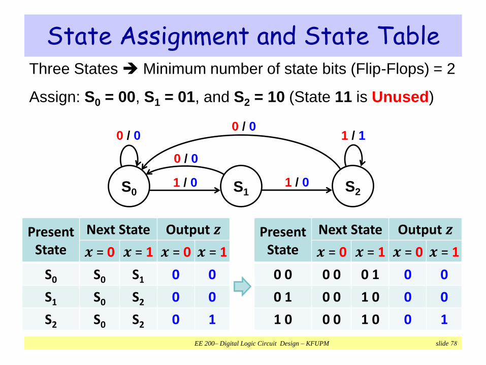
State Assignment and State TableThree States Minimum number of state bits (Flip-Flops) = 2
Assign: S0 = 00, S1 = 01, and S2 = 10 (State 11 is Unused)
0 / 0
0 / 0
S0
0 / 0
1 / 0 S11 / 0 S2
1 / 1
PresentState
Next State Output 𝒛
𝒙 = 0 𝒙 = 1 𝒙 = 0 𝒙 = 1
S0 S0 S1 0 0
S1 S0 S2 0 0
S2 S0 S2 0 1
PresentState
Next State Output 𝒛
𝒙 = 0 𝒙 = 1 𝒙 = 0 𝒙 = 1
0 0 0 0 0 1 0 0
0 1 0 0 1 0 0 0
1 0 0 0 1 0 0 1
EE 200– Digital Logic Circuit Design – KFUPM slide 79
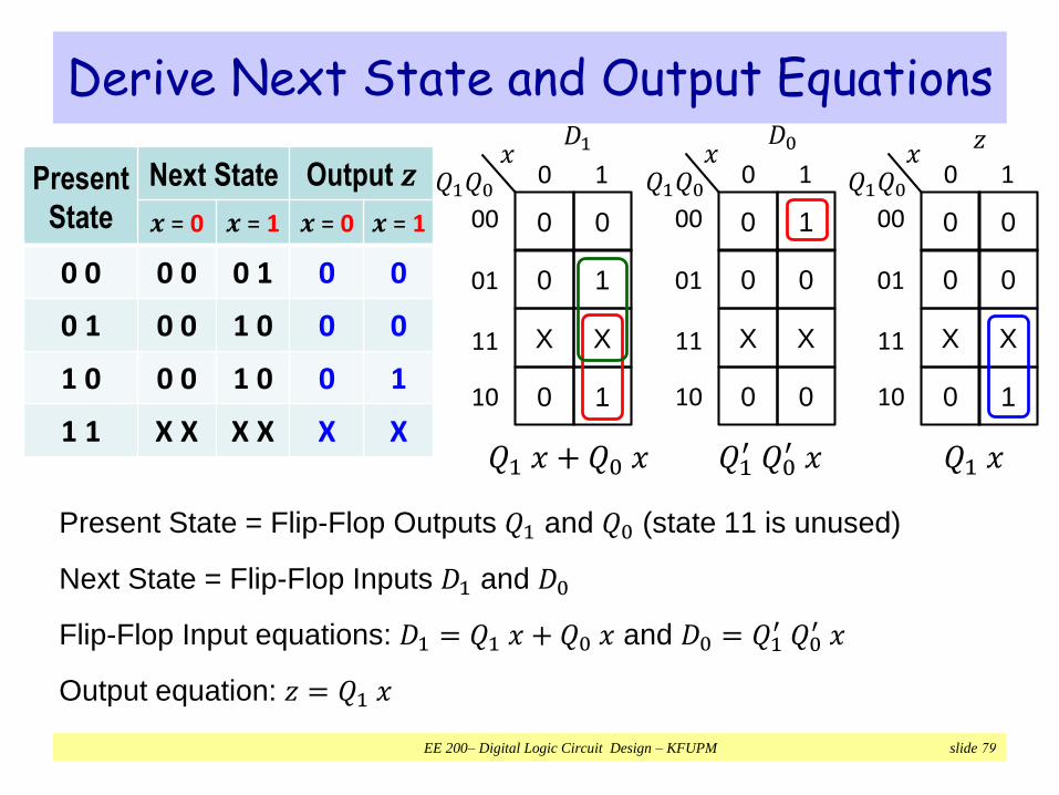
Derive Next State and Output Equations
Present State = Flip-Flop Outputs 𝑄1 and 𝑄0 (state 11 is unused)
Next State = Flip-Flop Inputs 𝐷1 and 𝐷0
Flip-Flop Input equations: 𝐷1 = 𝑄1 𝑥 + 𝑄0 𝑥 and 𝐷0 = 𝑄1′ 𝑄0
′ 𝑥
Output equation: 𝑧 = 𝑄1 𝑥
Present
State
Next State Output 𝒛
𝒙 = 0 𝒙 = 1 𝒙 = 0 𝒙 = 1
0 0 0 0 0 1 0 0
0 1 0 0 1 0 0 0
1 0 0 0 1 0 0 1
1 1 X X X X X X
𝑄1𝑄0𝑥
0 1
00
01
11
10
0 0
0 1
X X
0 1
𝐷1
𝑄1𝑄0𝑥
0 1
00
01
11
10
0 1
0 0
X X
0 0
𝐷0
𝑄1 𝑥 + 𝑄0 𝑥 𝑄1′ 𝑄0
′ 𝑥
𝑄1𝑄0𝑥
0 1
00
01
11
10
0 0
0 0
X X
0 1
𝑧
𝑄1 𝑥

EE 200– Digital Logic Circuit Design – KFUPM slide 80
𝐷1
𝑄1′
𝐷0𝑄0
𝑄0′
𝑄1
Reset
Draw the Mealy Sequence Detector Circuit
𝐷1 = 𝑄1 𝑥 + 𝑄0 𝑥 𝐷0 = 𝑄1′ 𝑄0
′ 𝑥 𝑧 = 𝑄1 𝑥
Output Logic
Next StateLogic
Next StateLogic
EE 200– Digital Logic Circuit Design – KFUPM slide 81
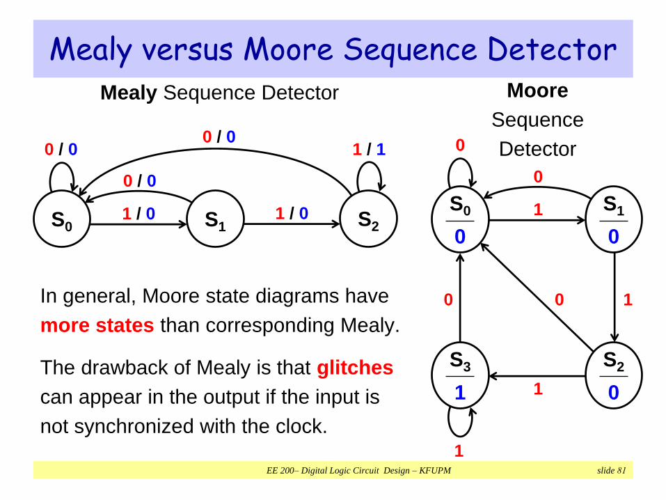
Mealy versus Moore Sequence Detector
In general, Moore state diagrams have
more states than corresponding Mealy.
The drawback of Mealy is that glitches
can appear in the output if the input is
not synchronized with the clock.
0 / 0
0 / 0
S0
0 / 0
1 / 0 S11 / 0 S2
1 / 1
0
0 0
S0
0
S1
0
S2
0
S3
1
1
1
1
0
1
Mealy Sequence Detector Moore
Sequence
Detector

EE 200– Digital Logic Circuit Design – KFUPM slide 82
Verification Sequential circuits should be verified by showing that the
circuit produces the original state diagram
Verification can be done manually, or with the help of a
simulation program
All possible input combinations are applied at each state
and the state variables and outputs are observed
A reset input is used to reset the circuit to its initial state
Apply a sequence of inputs to test all the state-input
combinations, i.e., all transitions in the state diagram
Observe the output and the next state that appears after
each clock edge in the timing diagram

EE 200– Digital Logic Circuit Design – KFUPM slide 83
Input Test Sequence
Required to verify the correct operation of a sequential circuit
It should test each state transition of the state diagram
Test sequences can be produced from the state diagram
Consider the Mealy sequence detector, starting at S0 (reset), we can
use an input test sequence to verify all state transitions:
Input test sequence: reset then x = 0, 1, 0, 1, 1, 0, 1, 1, 1, 1
0 / 0
0 / 0
S0
0 / 0
1 / 0 S1reset 1 / 0 S2
1 / 1Reset input
forces initial
state to be S0

EE 200– Digital Logic Circuit Design – KFUPM slide 84
Q0
Q1 S0 S0 S1 S0 S1 S2 S0 S1 S2 S2
Verifying the Mealy Sequence Detector
Input test sequence: reset then x = 0, 1, 0, 1, 1, 0, 1, 1, 1, 1
0 / 0
0 / 0
S0
0 / 0
1 / 0 S1reset 1 / 0 S2
1 / 1
z
reset
x 0 1 0 1 1 0 1 1 1 1
clock
cc0 cc1 cc2 cc3 cc4 cc5 cc6 cc7 cc8 cc9 cc10
0 0 0 0 0 0 0 0 1 1
glitch

EE 200– Digital Logic Circuit Design – KFUPM slide 85
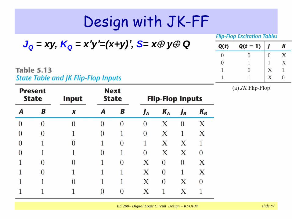
Design using JK-FF
When it comes to FF other than D-FF, the input
equations of the FF are derived from their excitation
tables and the state table.
Thus, we need to list the inputs that will cause the state
change in the state table.

EE 200– Digital Logic Circuit Design – KFUPM slide 86
Design using JK-FF
Synthesis is a design procedure that follows some
predefined steps. (well known procedure steps)
Computer SW for Hardware design uses synthesis to
come up with logic circuits from a set or behavioral
description.
EE 200– Digital Logic Circuit Design – KFUPM slide 87
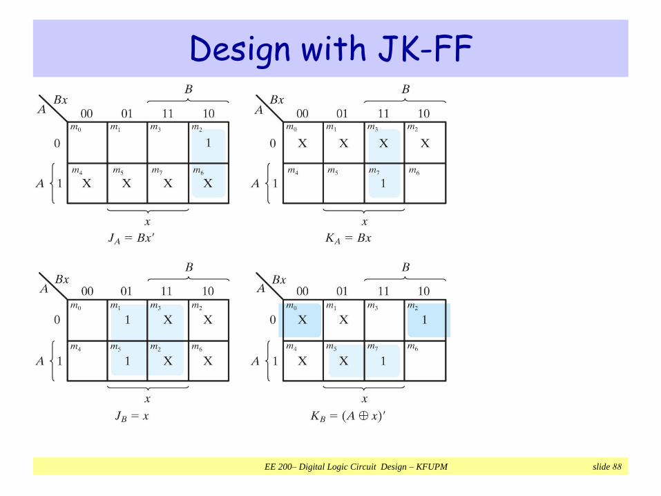
Design with JK-FF
JQ = xy, KQ = x’y’=(x+y)’, S= x y Q
EE 200– Digital Logic Circuit Design – KFUPM slide 88
Design with JK-FF

EE 200– Digital Logic Circuit Design – KFUPM slide 89
Design with JK-FF

EE 200– Digital Logic Circuit Design – KFUPM slide 90
Design of a Binary Counter
Problem Specification:
Design a circuit that counts up from 0 to 7 then back to 0
000 001 010 011 100 101 110 111 000
When reaching 7, the counter goes back to 0 then repeat
There is no input to the circuit
The counter is incremented each cycle
The output of the circuit is the present state (count value)
The circuit should be designed using T-type Flip-Flops

EE 200– Digital Logic Circuit Design – KFUPM slide 92
Designing the State Diagram
Eight states are needed to store the count values 0 to 7
No input, state transition happens at the edge of each
cycleS0
S4
S2S6
S1S7
S5 S3
Each state is
assigned a unique
binary count value
Three Flip-Flops
are required for
the eight states

EE 200– Digital Logic Circuit Design – KFUPM slide 93
State Table
Only two columns: Present State and Next
State
State changes each cycle
000
100
010110
001111
101 011
Present StateQ2 Q1 Q0
Next StateD2 D1 D0
0 0 0 0 0 1
0 0 1 0 1 0
0 1 0 0 1 1
0 1 1 1 0 0
1 0 0 1 0 1
1 0 1 1 1 0
1 1 0 1 1 1
1 1 1 0 0 0

EE 200– Digital Logic Circuit Design – KFUPM slide 94
Deriving the Next State Equations

EE 200– Digital Logic Circuit Design – KFUPM slide 95
3-Bit Counter Circuit Diagram