Switched Capacitor Voltage Converters - Microchip...
26
© 2010 Microchip Technology Inc. DS21488B-page 1 TCM828/TCM829 Features • Charge Pump in 5-Pin SOT-23 Package • >95% Voltage Conversion Efficiency • Voltage Inversion and/or Doubling • Low 50 μA (TCM828) Quiescent Current • Operates from +1.5V to +5.5V • Up to 25 mA Output Current • Only Two External Capacitors Required Applications • LCD Panel Bias • Cellular Phones • Pagers • PDAs, Portable Dataloggers • Battery-Powered Devices Typical Application Circuit Description The TCM828/TCM829 devices are CMOS “charge- pump” voltage converters in ultra-small, 5-Pin SOT-23 packages. They invert and/or double an input voltage which can range from +1.5V to +5.5V. Conversion efficiency is typically >95%. Switching frequency is 12 kHz for the TCM828, and 35 kHz for the TCM829. External component requirement is only two capacitors (3.3 μF nominal) for standard voltage inverter applications. With a few additional components, a positive doubler can also be built. All other circuitry, including control, oscillator and power MOSFETs, are integrated on-chip. Supply current is 50 μA (TCM828) and 115 μA (TCM829). The TCM828 and TCM829 devices are available in a 5-Pin SOT-23 surface mount package. Package Type Ordering Information V IN V - OUTPUT C + C - C1 C 2 INPUT GND TCM828/TCM829 Voltage Inverter OUT Part No. Package Temperature Range TCM828ECT 5-Pin SOT-23 -40°C to +85°C TCM828VT 5-Pin SOT-23 -40°C to +125°C TCM829ECT 5-Pin SOT-23 -40°C to +85°C Note: 5-Pin SOT-23 is equivalent to EIAJ SC-74A. C + 1 2 3 5 GND 4 C - OUT V IN TCM828/TCM829 SOT-23 Switched Capacitor Voltage Converters
-
Upload
nguyentuong -
Category
Documents
-
view
220 -
download
0
Transcript of Switched Capacitor Voltage Converters - Microchip...
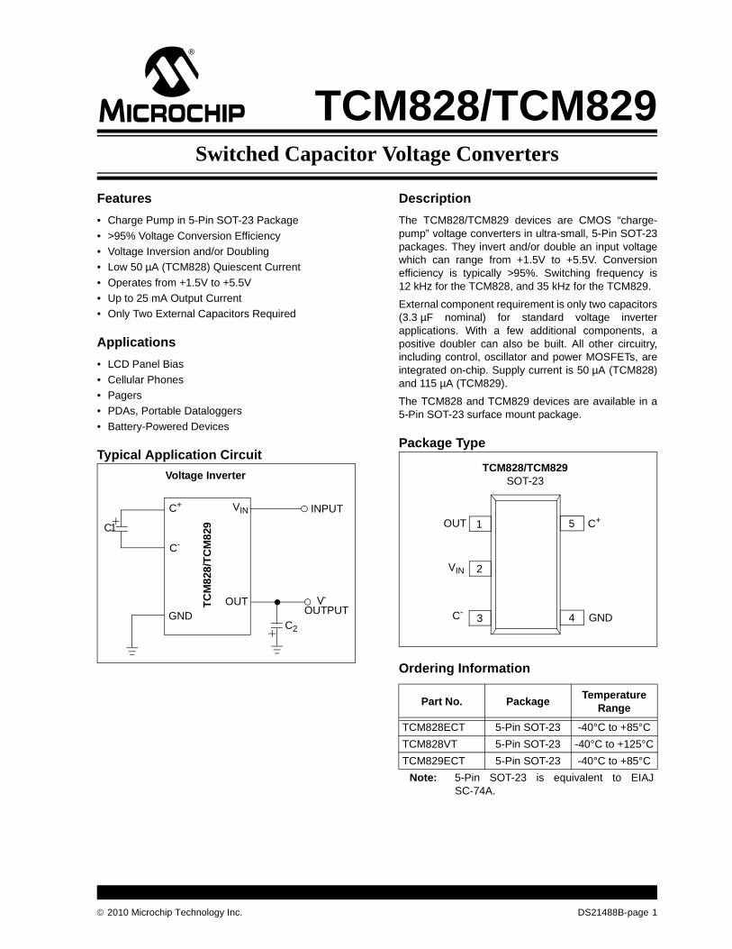
TCM828/TCM829Switched Capacitor Voltage Converters
Features• Charge Pump in 5-Pin SOT-23 Package• >95% Voltage Conversion Efficiency• Voltage Inversion and/or Doubling• Low 50 µA (TCM828) Quiescent Current• Operates from +1.5V to +5.5V• Up to 25 mA Output Current• Only Two External Capacitors Required
Applications• LCD Panel Bias• Cellular Phones• Pagers• PDAs, Portable Dataloggers• Battery-Powered Devices
Typical Application Circuit
DescriptionThe TCM828/TCM829 devices are CMOS “charge-pump” voltage converters in ultra-small, 5-Pin SOT-23packages. They invert and/or double an input voltagewhich can range from +1.5V to +5.5V. Conversionefficiency is typically >95%. Switching frequency is12 kHz for the TCM828, and 35 kHz for the TCM829.
External component requirement is only two capacitors(3.3 µF nominal) for standard voltage inverterapplications. With a few additional components, apositive doubler can also be built. All other circuitry,including control, oscillator and power MOSFETs, areintegrated on-chip. Supply current is 50 µA (TCM828)and 115 µA (TCM829).
The TCM828 and TCM829 devices are available in a5-Pin SOT-23 surface mount package.
Package Type
Ordering Information
VIN
V-OUTPUT
C+
C-
C1
C2
INPUT
GND
TCM
828/
TCM
829
Voltage Inverter
OUT
Part No. Package Temperature Range
TCM828ECT 5-Pin SOT-23 -40°C to +85°CTCM828VT 5-Pin SOT-23 -40°C to +125°CTCM829ECT 5-Pin SOT-23 -40°C to +85°C
Note: 5-Pin SOT-23 is equivalent to EIAJSC-74A.
C+1
2
3
5
GND4C-
OUT
VIN
TCM828/TCM829SOT-23
© 2010 Microchip Technology Inc. DS21488B-page 1

TCM828/TCM829
NOTES:DS21488B-page 2 © 2010 Microchip Technology Inc.
TCM828/TCM829
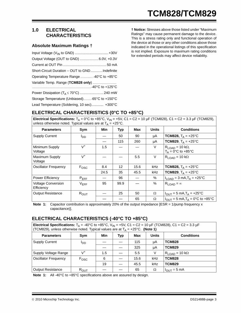
1.0 ELECTRICAL CHARACTERISTICS
Absolute Maximum Ratings †Input Voltage (VIN to GND) ..................................+30V
Output Voltage (OUT to GND) ...................6.0V, +0.3V
Current at OUT Pin ............................................ 50 mA
Short-Circuit Duration – OUT to GND............Indefinite
Operating Temperature Range ................ -40°C to +85°C
Variable Temp. Range (TCM828 only) ............................................................................................................-40°C to +125°C
Power Dissipation (TA ≤ 70°C) ........................ 240 mW
Storage Temperature (Unbiased)..........-65°C to +150°C
Lead Temperature (Soldering, 10 sec)............ +300°C
† Notice: Stresses above those listed under “MaximumRatings” may cause permanent damage to the device.This is a stress rating only and functional operation ofthe device at those or any other conditions above thoseindicated in the operational listings of this specificationis not implied. Exposure to maximum rating conditionsfor extended periods may affect device reliability.
ELECTRICAL CHARACTERISTICS (0°C TO +85°C)Electrical Specifications: TA = 0°C to +85°C, VIN = +5V, C1 = C2 = 10 µF (TCM828), C1 = C2 = 3.3 µF (TCM829), unless otherwise noted. Typical values are at TA = +25°C.
Parameters Sym Min Typ Max Units Conditions
Supply Current IDD — 50 90 µA TCM828, TA = +25°C— 115 260 µA TCM829, TA = +25°C
Minimum Supply Voltage
V+ 1.5 — — V RLOAD = 10 kΩ,TA = 0°C to +85°C
Maximum Supply Voltage
V+ — — 5.5 V RLOAD = 10 kΩ
Oscillator Frequency FOSC 8.4 12 15.6 kHz TCM828, TA = +25°C24.5 35 45.5 kHz TCM829, TA = +25°C
Power Efficiency PEFF — 96 — % ILOAD = 3 mA,TA = +25°CVoltage Conversion Efficiency
VEFF 95 99.9 — % RLOAD = ∞
Output Resistance ROUT — 25 50 Ω IOUT = 5 mA,TA = +25°C— — 65 Ω IOUT = 5 mA,TA = 0°C to +85°C
Note 1: Capacitor contribution is approximately 20% of the output impedance [ESR = 1/pump frequency x capacitance)].
ELECTRICAL CHARACTERISTICS (-40°C TO +85°C)Electrical Specifications: TA = -40°C to +85°C, VIN = +5V, C1 = C2 = 10 µF (TCM828), C1 = C2 = 3.3 µF (TCM829), unless otherwise noted. Typical values are at TA = +25°C. (Note 1)
Parameters Sym Min Typ Max Units Conditions
Supply Current IDD — — 115 µA TCM828— — 325 µA TCM829
Supply Voltage Range V+ 1.5 — 5.5 V RLOAD = 10 kΩOscillator Frequency FOSC 6 — 15.6 kHz TCM828
19 — 45.5 kHz TCM829Output Resistance ROUT — — 65 Ω IOUT = 5 mANote 1: All -40°C to +85°C specifications above are assured by design.
© 2010 Microchip Technology Inc. DS21488B-page 3

TCM828/TCM829
NOTES:DS21488B-page 4 © 2010 Microchip Technology Inc.
TCM828/TCM829
2.0 TYPICAL CHARACTERISTICS
Note: Circuit of Figure 5-3, VIN = +5V, C1 = C2 = C3, TA = +25°C, unless otherwise noted.
FIGURE 2-1: Output Resistance vs. Supply Voltage.
FIGURE 2-2: Output Resistance vs. Temperature.
FIGURE 2-3: TCM828 – Output Current vs. Capacitance.
FIGURE 2-4: TCM829 – Output Current vs. Capacitance.
Note: The graphs and tables provided following this note are a statistical summary based on a limited number ofsamples and are provided for informational purposes only. The performance characteristics listed hereinare not tested or guaranteed. In some graphs or tables, the data presented may be outside the specified-operating range (e.g., outside specified power supply range) and therefore outside the warranted range.
60
50
40
30
20
0
10
1.5 2.5 3.5 4.5SUPPLY VOLTAGE (V)
70
OU
TPU
T R
ESIS
TAN
CE
(Ω)
TCM829TCM828
70
60
50
40
30
0
20
10
–40°C 0°C 25°C 85°CTEMPERATURE (°C)
80
OU
TPU
T R
ESIS
TAN
CE
(Ω)
VIN = 1.5V
VIN = 3.3V
VIN = 5.0V
40
35
30
25
20
5
0
15
10
0 10 20 30 40
CAPACITANCE (µF)
OU
TPU
T C
UR
REN
T (m
A)
VIN = 4.75V, VOUT = – 4.0V
VIN = 3.15V, VOUT = – 2.5V
VIN = 1.9V, VOUT = –1.5V
35
30
25
20
5
0
15
10
0 105 15 20 25 3530CAPACITANCE (µF)
40
OU
TPU
T C
UR
REN
T (m
A)
VIN = 4.75V, V– = – 4.0V
VIN = 1.9V, VOUT = – 1.5V
VIN = 3.15V, V– = – 2.5V
© 2010 Microchip Technology Inc. DS21488B-page 5
TCM828/TCM829
Note:Circuit of Figure 5-3, VIN = +5V, C1 = C2 = C3, TA = +25°C, unless otherwise noted.FIGURE 2-5: TCM828 – Output Voltage Ripple vs. Capacitance.
FIGURE 2-6: TCM829 – Output Voltage Ripple vs. Capacitance.
FIGURE 2-7: Supply Current vs. Supply Voltage.
FIGURE 2-8: TCM828 – Pump Frequency vs. Temperature.
FIGURE 2-9: TCM829 – Pump Frequency vs. Temperature.
FIGURE 2-10: Output Voltage vs. Output Current.
450
400
350
300
250
50
0
200
150
100
0 105 25 20 25 30 35CAPACITANCE (µF)
OU
TPU
T VO
LTA
GE
RIP
PLE
(mVp
-p)
VIN = 4.75V, VOUT = – 4.0V
VIN = 3.15V, VOUT = – 2.5V
VIN = 1.9V, VOUT = – 1.5V
0 105 15 20 30 35CAPACITANCE (µF)
300
250
200
150
100
50
0OU
TPU
T VO
LTA
GE
RIP
PLE
(mVp
-p)
VIN = 4.75V, VOUT = – 4.0V
VIN = 3.15V, VOUT = – 2.5V
VIN = 1.9V, VOUT = – 1.5V
100
80
60
40
20
01.5 2.5 32 3.5 4 4.5 5 5.5
SUPPLY VOLTAGE (V)
120
SUPP
LY C
UR
REN
T (µ
A)
TCM829
TCM828
14
12
10
8
2
0
6
4
–40 0°C 25°C 85°CTEMPERATURE (°C)
PUM
P FR
EQU
ENC
Y (k
Hz)
5
VIN = 5.0V
VIN = 3.3V
VIN = 1.5V
–40°C 0°C 25°C 85°C
40
30
35
20
15
25
0
10
5
TEMPERATURE (°C)
45
PUM
P FR
EQU
ENC
Y (k
Hz)
VIN = 5.0V
VIN = 3.3V
VIN = 1.5V
–1
–2
–3
–4
–5
–60 20 3010 40 50
OUTPUT CURRENT (mA)
p0
OU
TPU
T VO
LTA
GE
(V)
VIN = 2.0V
VIN = 3.3V
VIN = 5.0V
DS21488B-page 6 © 2010 Microchip Technology Inc.

TCM828/TCM829
Note: Circuit of Figure 5-3, VIN = +5V, C1 = C2 = C3, TA = +25°C, unless otherwise noted.FIGURE 2-11: Efficiency vs. Output Current.
100
80
60
400 10 20 30 40 50
OUTPUT CURRENT (mA)
y p
EFFI
CIE
NC
Y (%
)VIN = 5.0V
VIN = 3.3VVIN =1.5V
© 2010 Microchip Technology Inc. DS21488B-page 7

TCM828/TCM829
NOTES:DS21488B-page 8 © 2010 Microchip Technology Inc.
TCM828/TCM829
3.0 PIN DESCRIPTIONThe descriptions of the pins are listed in Table 3-1.
TABLE 3-1: PIN FUNCTION TABLETCM828/TCM829
SOT-23 Symbol Function
1 OUT Inverting charge pump output2 VIN Positive power supply input3 C1
- Commutation capacitor negative terminal4 GND Ground5 C1
+ Commutation capacitor positive terminal
© 2010 Microchip Technology Inc. DS21488B-page 9
TCM828/TCM829
NOTES:DS21488B-page 10 © 2010 Microchip Technology Inc.

TCM828/TCM829
4.0 DETAILED DESCRIPTIONThe TCM828/TCM829 charge pump converters invertthe voltage applied to the VIN pin. Conversion consistsof a two phase operation (Figure 4-1). During the firstphase, switches S2 and S4 are open, while S1 and S3are closed. During this time, C1 charges to the voltageon VIN and load current is supplied from C2. During thesecond phase, S2 and S4 are closed, and S1 and S3are open. This action connects C1 across C2, restoringcharge to C2.
FIGURE 4-1: Ideal Switched Capacitor Charge Pump.
VOUT = -(VIN)
C1
C2
INS1
S3 S4
S2TCM828/TCM829
© 2010 Microchip Technology Inc. DS21488B-page 11

TCM828/TCM829
NOTES:DS21488B-page 12 © 2010 Microchip Technology Inc.
TCM828/TCM829
5.0 APPLICATIONS INFORMATION
5.0.1 OUTPUT VOLTAGE CONSIDERATIONS
The TCM828/TCM829 devices perform voltageconversion, but do not provide regulation. The outputvoltage will droop in a linear manner with respect toload current. The value of this equivalent outputresistance is approximately 25Ω nominal at +25°C andVIN = +5V. VOUT is approximately – 5V at light loads,and droops according to the equation below:
VDROOP = IOUT × ROUT
VOUT = –(VIN –VDROOP)
5.0.2 CHARGE PUMP EFFICIENCYThe overall power efficiency of the charge pump isaffected by four factors:
1. Losses from power consumed by the internaloscillator, switch drive, etc. (which vary withinput voltage, temperature and oscillatorfrequency).
2. I2R losses due to the on-resistance of theMOSFET switches on-board the charge pump.
3. Charge pump capacitor losses due to effectiveseries resistance (ESR).
4. Losses that occur during charge transfer (fromthe commutation capacitor to the outputcapacitor) when a voltage difference betweenthe two capacitors exists.
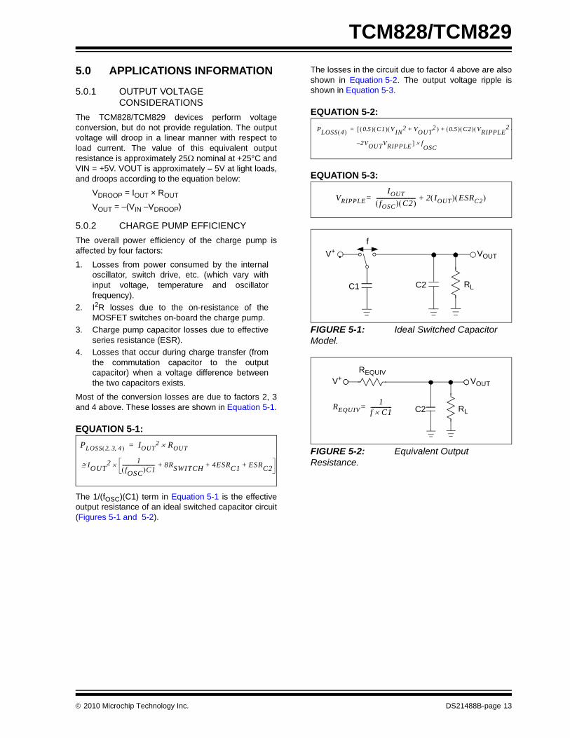
Most of the conversion losses are due to factors 2, 3and 4 above. These losses are shown in Equation 5-1.
EQUATION 5-1:
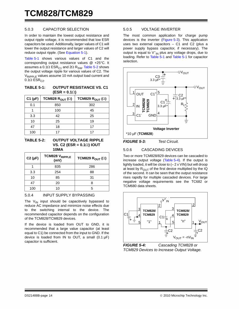
The 1/(fOSC)(C1) term in Equation 5-1 is the effectiveoutput resistance of an ideal switched capacitor circuit(Figures 5-1 and 5-2).
The losses in the circuit due to factor 4 above are alsoshown in Equation 5-2. The output voltage ripple isshown in Equation 5-3.
EQUATION 5-2:
EQUATION 5-3:
FIGURE 5-1: Ideal Switched Capacitor Model.
FIGURE 5-2: Equivalent Output Resistance.IOUT
2 1fOSC( )C1
-------------------------- 8RSWITCH 4ESRC1 ESRC2+ + +×≅
PLOSS 2 3 4, ,( ) IOUT2 ROUT×=
2VOUTVRIPPLE ]– f×OSC
PLOSS 4( ) 0.5( ) C1( ) V( IN2 VOUT2 ) 0.5( ) C2( ) VRIPPLE
2 –(+ +[=
VRIPPLEIOUT
fOSC( ) C2( )---------------------------- 2 IOUT( ) ESRC2( )+=
V+ VOUT
RLC1 C2
f
V+ VOUT
REQUIV
RLC2REQUIV1
f C1×---------------=
© 2010 Microchip Technology Inc. DS21488B-page 13
TCM828/TCM829
5.0.3 CAPACITOR SELECTIONIn order to maintain the lowest output resistance andoutput ripple voltage, it is recommended that low ESRcapacitors be used. Additionally, larger values of C1 willlower the output resistance and larger values of C2 willreduce output ripple. (See Equation 5-1).Table 5-1 shows various values of C1 and thecorresponding output resistance values @ +25°C. Itassumes a 0.1Ω ESRC1 and 2Ω RSW. Table 5-2 showsthe output voltage ripple for various values of C2. TheVRIPPLE values assume 10 mA output load current and0.1Ω ESRC2.
I
5.0.4 INPUT SUPPLY BYPASSINGThe VIN input should be capacitively bypassed toreduce AC impedance and minimize noise effects dueto the switching internal to the device. Therecommended capacitor depends on the configurationof the TCM828/TCM829 devices.
If the device is loaded from OUT to GND, it isrecommended that a large value capacitor (at leastequal to C1) be connected from the input to GND. If thedevice is loaded from IN to OUT, a small (0.1 µF)capacitor is sufficient.
5.0.5 VOLTAGE INVERTERThe most common application for charge pumpdevices is the inverter (Figure 5-3). This applicationuses two external capacitors – C1 and C2 (plus apower supply bypass capacitor, if necessary). Theoutput is equal to V–
IN plus any voltage drops, due toloading. Refer to Table 5-1 and Table 5-1 for capacitorselection.
FIGURE 5-3: Test Circuit.
5.0.6 CASCADING DEVICESTwo or more TCM828/829 devices can be cascaded toincrease output voltage (Table 5-4). If the output islightly loaded, it will be close to (– 2 x VIN) but will droopat least by ROUT of the first device multiplied by the IQof the second. It can be seen that the output resistancerises rapidly for multiple cascaded devices. For largenegative voltage requirements see the TC682 orTCM680 data sheets.
FIGURE 5-4: Cascading TCM828 or TCM829 Devices to Increase Output Voltage.
TABLE 5-1: OUTPUT RESISTANCE VS. C1 (ESR = 0.1Ω)
C1 (µF) TCM828 ROUT (Ω) TCM829 ROUT (Ω)
0.1 850 3021 100 45
3.3 42 2510 25 1947 18 17
100 17 17
TABLE 5-2: OUTPUT VOLTAGE RIPPLE VS. C2 (ESR = 0.1Ω) IOUT 10MA
C2 (µF) TCM828 VRIPPLE (mV) TCM829 ROUT (Ω)
1 835 2863.3 254 8810 85 3147 20 8
100 10 5
3
2
4
51
C33.3 µF*
C13.3 µF*
C23.3 µF*
VOUT
VOUT
RL
C1-
IN
OUT C1+
GND
Voltage Inverter
TCM
828/
TCM
829
*10 µF (TCM828)
C1C1
C2
5 5
4
3
4
1
2 2
1
3
C2
V+IN
VOUT
VOUT = -nVIN
"1" "n"
. . .
. . .
TCM828/TCM829
TCM828/TCM829
DS21488B-page 14 © 2010 Microchip Technology Inc.
TCM828/TCM829
5.0.7 PARALLELING DEVICESTo reduce the value of ROUT, multiple TCM828/TCM829 devices can be connected in parallel(Figure 5-5). The output resistance will be reduced bya factor of N, where N is the number of TCM828/TCM829 device. Each device will require it’s own pumpcapacitor (C1), but all devices may share one reservoircapacitor (C2). However, to preserve rippleperformance, the value of C2 should be scaledaccording to the number of paralleled TCM828/TCM829 devices.FIGURE 5-5: Paralleling TCM828 or TCM829 Devices to Reduce Output Resistance.
5.0.8 VOLTAGE DOUBLER/INVERTERAnother common application of the TCM828/TCM829devices is shown in Figure 5-6. This circuit performstwo functions in combination. C1 and C2 form thestandard inverter circuit described above. C3 and C4,plus the two diodes, form the voltage doubler circuit. C1and C3 are the pump capacitors, while C2 and C4 arethe reservoir capacitors. Because both sub-circuits relyon the same switches, if either output is loaded, bothwill drop toward GND. Make sure that the total currentdrawn from both the outputs does not total more than40 mA.
FIGURE 5-6: Combined Doubler and Inverter.
5.0.9 DIODE PROTECTION FOR HEAVY LOADS
When heavy loads require the OUT pin to sink largecurrents, being delivered by a positive source, diodeprotection may be needed. The OUT pin should not beallowed to be pulled above ground. This isaccomplished by connecting a Schottky diode(1N5817) as shown in Figure 5-7.
FIGURE 5-7: High V– Load Current.
5.0.10 LAYOUT CONSIDERATIONSAs with any switching power supply circuit, good layoutpractice is recommended. Mount components as closetogether as possible, to minimize stray inductance andcapacitance. Also use a large ground plane to minimizenoise leakage into other circuitry.
C1C1
5 5
4
3
4
1
2 2
1
3
C2
V+IN
VOUT
VOUT = V-IN
"1" "n"
. . .
. . .
TCM828/TCM829
TCM828/TCM829
ROUT = VOUT OF SINGLE DEVICENUMBER OF DEVICES
C1
D1
D2
D1, D2 = 1N4148
5
4
1
23
C2
C4C3
V+IN
VOUT = V-IN
VOUT = (2VIN) -
TCM828/TCM829
(VFD1) - (VFD2)
GND
OUT
4
1
TCM828/TCM829
© 2010 Microchip Technology Inc. DS21488B-page 15

TCM828/TCM829
NOTES:DS21488B-page 16 © 2010 Microchip Technology Inc.
TCM828/TCM829
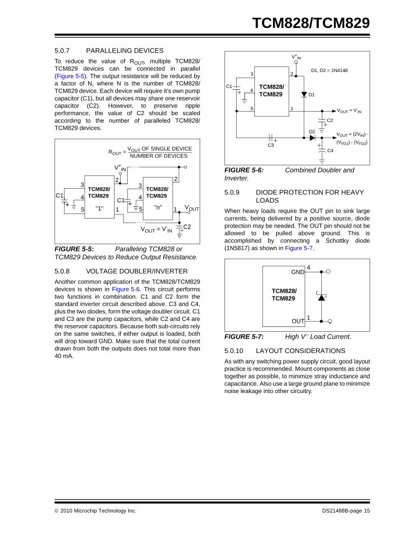
6.0 PACKAGING INFORMATION
6.1 Package Marking Information
Legend: XX...X Customer-specific informationY Year code (last digit of calendar year)YY Year code (last 2 digits of calendar year)WW Week code (week of January 1 is week ‘01’)NNN Alphanumeric traceability code Pb-free JEDEC designator for Matte Tin (Sn)* This package is Pb-free. The Pb-free JEDEC designator ( )
can be found on the outer packaging for this package.
Note: In the event the full Microchip part number cannot be marked on one line, it willbe carried over to the next line, thus limiting the number of availablecharacters for customer-specific information.
3e
3e
5-Lead SOT-23 Example:
XXNN CA25
Device Code
TCM828ECT728 CANNTCM828VT713 CWNNTCM829ECT713-GVAO CBNN
© 2010 Microchip Technology Inc. DS21488B-page 17

TCM828/TCM829
FIGURE 6-1: Component Taping Orientation for 5-Pin SOT-23 (EIAJ SC-74A) Devices.
User Direction of Feed User Direction of Feed
DeviceMarking Device
Marking
PIN 1
PIN 1
Standard Reel Component OrientationTR Suffix Device(Mark Right Side Up)
Reverse Reel Component OrientationRT Suffix Device(Mark Upside Down)
W
P
Package Carrier Width (W) Pitch (P) Part Per Full Reel Reel Size
5-Pin SOT-23 8 mm 4 mm 3000 7 in
Carrier Tape, Number of Components Per Reel and Reel Size
DS21488B-page 18 © 2010 Microchip Technology Inc.

TCM828/TCM829
���������� ��������� �������� ������������������
�������� �� ��!��!�����"�#��"��$�����%"�� �"�&��!����$%!��!����"�&��!����$%!��!�!������$��'���"������� ����!�"���� �� ��!��������"�$���������������#�(������
)�*+ )�!����� ��!���� ���$��������'��$�,��%��!�-��-�$�%$�$������!�
����� .�$��� !$��%��$����/����"�-���!0�����!��!���$�����������1��/�����������&���$������$�"��$��$$�+22---� �������� 2���/�����
3��$! ��44��# #���� ��!���4� �$! ��5 56� ��7
5% 8��&�1��! 5 �4��"�1�$�� � �����)�*6%$!�"��4��"�1�$�� �� �����)�*6,�����9����$ � ���� : ������"�"�1��/���� ���/��!! �� ��;� : �����$��"&& �� ���� : ����6,�����<�"$� # ���� : ������"�"�1��/����<�"$� #� ���� : ��;�6,�����4���$� � ���� : ����.$�4���$� 4 ���� : ��=�.$���$ 4� ���� : ��;�.$������ � �> : ��>4��"� ���/��!! � ���; : ���=4��"�<�"$� 8 ���� : ����
φ
Nb
E
E1
D
1 2 3
e
e1
A
A1
A2 c
L
L1
������� ������� ��-��� *������)
© 2010 Microchip Technology Inc. DS21488B-page 19
TCM828/TCM829
5-Lead Plastic Small Outline Transistor (CT) [SOT-23]
Note: For the most current package drawings, please see the Microchip Packaging Specification located at http://www.microchip.com/packaging
DS21488B-page 20 © 2010 Microchip Technology Inc.

TCM828/TCM829
APPENDIX A: REVISION HISTORY
Revision B (August 2010)The following is the list of modifications:
1. Added new operating temperature for TCM828(TCM828VT).
2. Reformatted the original document. 3. Updated package drawings.
Revision A (March 2001)• Original Release of this Document.
© 2010 Microchip Technology Inc. DS21488B-page 21

TCM828/TCM829
NOTES:DS21488B-page 22 © 2010 Microchip Technology Inc.

TCM828/TCM829
PRODUCT IDENTIFICATION SYSTEMTo order or obtain information, e.g., on pricing or delivery, refer to the factory or the listed sales office.
PART NO. X /XX
PackageTemperatureRange
Device
Device: TCM828: CMOS Voltage Converter.TCM829: CMOS Voltage Converter.
Temperature Range: E = -40°C to +85°CV = -40°C to +125°C
Package: CT = 5-Lead Plastic Small Outline Transistor, SOT-23.
Examples:
a) TCM828ECT728: Extended Temp., 5-LD SOT-23 Package.
b) TCM828VT713: Various Temperature5-LD SOT-23 Package.
c) TCM829ECT713-GVAO:Extended Temp.,5-LD SOT-23 Package.
© 2010 Microchip Technology Inc. DS21488B-page 23

TCM828/TCM829
NOTES:DS21488B-page 24 © 2010 Microchip Technology Inc.
Note the following details of the code protection feature on Microchip devices:• Microchip products meet the specification contained in their particular Microchip Data Sheet.
• Microchip believes that its family of products is one of the most secure families of its kind on the market today, when used in the intended manner and under normal conditions.
• There are dishonest and possibly illegal methods used to breach the code protection feature. All of these methods, to our knowledge, require using the Microchip products in a manner outside the operating specifications contained in Microchip’s Data Sheets. Most likely, the person doing so is engaged in theft of intellectual property.
• Microchip is willing to work with the customer who is concerned about the integrity of their code.
• Neither Microchip nor any other semiconductor manufacturer can guarantee the security of their code. Code protection does not mean that we are guaranteeing the product as “unbreakable.”
Code protection is constantly evolving. We at Microchip are committed to continuously improving the code protection features of ourproducts. Attempts to break Microchip’s code protection feature may be a violation of the Digital Millennium Copyright Act. If such actsallow unauthorized access to your software or other copyrighted work, you may have a right to sue for relief under that Act.
Information contained in this publication regarding deviceapplications and the like is provided only for your convenienceand may be superseded by updates. It is your responsibility toensure that your application meets with your specifications.MICROCHIP MAKES NO REPRESENTATIONS ORWARRANTIES OF ANY KIND WHETHER EXPRESS ORIMPLIED, WRITTEN OR ORAL, STATUTORY OROTHERWISE, RELATED TO THE INFORMATION,INCLUDING BUT NOT LIMITED TO ITS CONDITION,QUALITY, PERFORMANCE, MERCHANTABILITY ORFITNESS FOR PURPOSE. Microchip disclaims all liabilityarising from this information and its use. Use of Microchipdevices in life support and/or safety applications is entirely atthe buyer’s risk, and the buyer agrees to defend, indemnify andhold harmless Microchip from any and all damages, claims,suits, or expenses resulting from such use. No licenses areconveyed, implicitly or otherwise, under any Microchipintellectual property rights.
© 2010 Microchip Technology Inc.
Trademarks
The Microchip name and logo, the Microchip logo, dsPIC, KEELOQ, KEELOQ logo, MPLAB, PIC, PICmicro, PICSTART, PIC32 logo, rfPIC and UNI/O are registered trademarks of Microchip Technology Incorporated in the U.S.A. and other countries.
FilterLab, Hampshire, HI-TECH C, Linear Active Thermistor, MXDEV, MXLAB, SEEVAL and The Embedded Control Solutions Company are registered trademarks of Microchip Technology Incorporated in the U.S.A.
Analog-for-the-Digital Age, Application Maestro, CodeGuard, dsPICDEM, dsPICDEM.net, dsPICworks, dsSPEAK, ECAN, ECONOMONITOR, FanSense, HI-TIDE, In-Circuit Serial Programming, ICSP, Mindi, MiWi, MPASM, MPLAB Certified logo, MPLIB, MPLINK, mTouch, Octopus, Omniscient Code Generation, PICC, PICC-18, PICDEM, PICDEM.net, PICkit, PICtail, REAL ICE, rfLAB, Select Mode, Total Endurance, TSHARC, UniWinDriver, WiperLock and ZENA are trademarks of Microchip Technology Incorporated in the U.S.A. and other countries.
SQTP is a service mark of Microchip Technology Incorporated in the U.S.A.
All other trademarks mentioned herein are property of their respective companies.
© 2010, Microchip Technology Incorporated, Printed in the U.S.A., All Rights Reserved.
Printed on recycled paper.
ISBN: 978-1-60932-445-2
DS21488B-page 25
Microchip received ISO/TS-16949:2002 certification for its worldwide headquarters, design and wafer fabrication facilities in Chandler and Tempe, Arizona; Gresham, Oregon and design centers in California and India. The Company’s quality system processes and procedures are for its PIC® MCUs and dsPIC® DSCs, KEELOQ® code hopping devices, Serial EEPROMs, microperipherals, nonvolatile memory and analog products. In addition, Microchip’s quality system for the design and manufacture of development systems is ISO 9001:2000 certified.

DS21488B-page 26 © 2010 Microchip Technology Inc.
AMERICASCorporate Office2355 West Chandler Blvd.Chandler, AZ 85224-6199Tel: 480-792-7200 Fax: 480-792-7277Technical Support: http://support.microchip.comWeb Address: www.microchip.comAtlantaDuluth, GA Tel: 678-957-9614 Fax: 678-957-1455BostonWestborough, MA Tel: 774-760-0087 Fax: 774-760-0088ChicagoItasca, IL Tel: 630-285-0071 Fax: 630-285-0075ClevelandIndependence, OH Tel: 216-447-0464 Fax: 216-447-0643DallasAddison, TX Tel: 972-818-7423 Fax: 972-818-2924DetroitFarmington Hills, MI Tel: 248-538-2250Fax: 248-538-2260KokomoKokomo, IN Tel: 765-864-8360Fax: 765-864-8387Los AngelesMission Viejo, CA Tel: 949-462-9523 Fax: 949-462-9608Santa ClaraSanta Clara, CA Tel: 408-961-6444Fax: 408-961-6445TorontoMississauga, Ontario, CanadaTel: 905-673-0699 Fax: 905-673-6509
ASIA/PACIFICAsia Pacific OfficeSuites 3707-14, 37th FloorTower 6, The GatewayHarbour City, KowloonHong KongTel: 852-2401-1200Fax: 852-2401-3431Australia - SydneyTel: 61-2-9868-6733Fax: 61-2-9868-6755China - BeijingTel: 86-10-8528-2100 Fax: 86-10-8528-2104China - ChengduTel: 86-28-8665-5511Fax: 86-28-8665-7889China - ChongqingTel: 86-23-8980-9588Fax: 86-23-8980-9500China - Hong Kong SARTel: 852-2401-1200 Fax: 852-2401-3431China - NanjingTel: 86-25-8473-2460Fax: 86-25-8473-2470China - QingdaoTel: 86-532-8502-7355Fax: 86-532-8502-7205China - ShanghaiTel: 86-21-5407-5533 Fax: 86-21-5407-5066China - ShenyangTel: 86-24-2334-2829Fax: 86-24-2334-2393China - ShenzhenTel: 86-755-8203-2660 Fax: 86-755-8203-1760China - WuhanTel: 86-27-5980-5300Fax: 86-27-5980-5118China - XianTel: 86-29-8833-7252Fax: 86-29-8833-7256China - XiamenTel: 86-592-2388138 Fax: 86-592-2388130China - ZhuhaiTel: 86-756-3210040 Fax: 86-756-3210049
ASIA/PACIFICIndia - BangaloreTel: 91-80-3090-4444 Fax: 91-80-3090-4123India - New DelhiTel: 91-11-4160-8631Fax: 91-11-4160-8632India - PuneTel: 91-20-2566-1512Fax: 91-20-2566-1513Japan - YokohamaTel: 81-45-471- 6166 Fax: 81-45-471-6122Korea - DaeguTel: 82-53-744-4301Fax: 82-53-744-4302Korea - SeoulTel: 82-2-554-7200Fax: 82-2-558-5932 or 82-2-558-5934Malaysia - Kuala LumpurTel: 60-3-6201-9857Fax: 60-3-6201-9859Malaysia - PenangTel: 60-4-227-8870Fax: 60-4-227-4068Philippines - ManilaTel: 63-2-634-9065Fax: 63-2-634-9069SingaporeTel: 65-6334-8870Fax: 65-6334-8850Taiwan - Hsin ChuTel: 886-3-6578-300Fax: 886-3-6578-370Taiwan - KaohsiungTel: 886-7-213-7830Fax: 886-7-330-9305Taiwan - TaipeiTel: 886-2-2500-6610 Fax: 886-2-2508-0102Thailand - BangkokTel: 66-2-694-1351Fax: 66-2-694-1350
EUROPEAustria - WelsTel: 43-7242-2244-39Fax: 43-7242-2244-393Denmark - CopenhagenTel: 45-4450-2828 Fax: 45-4485-2829France - ParisTel: 33-1-69-53-63-20 Fax: 33-1-69-30-90-79Germany - MunichTel: 49-89-627-144-0 Fax: 49-89-627-144-44Italy - Milan Tel: 39-0331-742611 Fax: 39-0331-466781Netherlands - DrunenTel: 31-416-690399 Fax: 31-416-690340Spain - MadridTel: 34-91-708-08-90Fax: 34-91-708-08-91UK - WokinghamTel: 44-118-921-5869Fax: 44-118-921-5820
WORLDWIDE SALES AND SERVICE
07/15/10