CC3200 SimpleLink Wi-Fi and IoT Solution with MCU LaunchPad ...
Product
Folder
Order
Now
Technical
Documents
Tools &
Software
Support &Community
An IMPORTANT NOTICE at the end of this data sheet addresses availability, warranty, changes, use in safety-critical applications,intellectual property matters and other important disclaimers. PRODUCTION DATA.
CC3220SWAS035A –SEPTEMBER 2016–REVISED FEBRUARY 2017
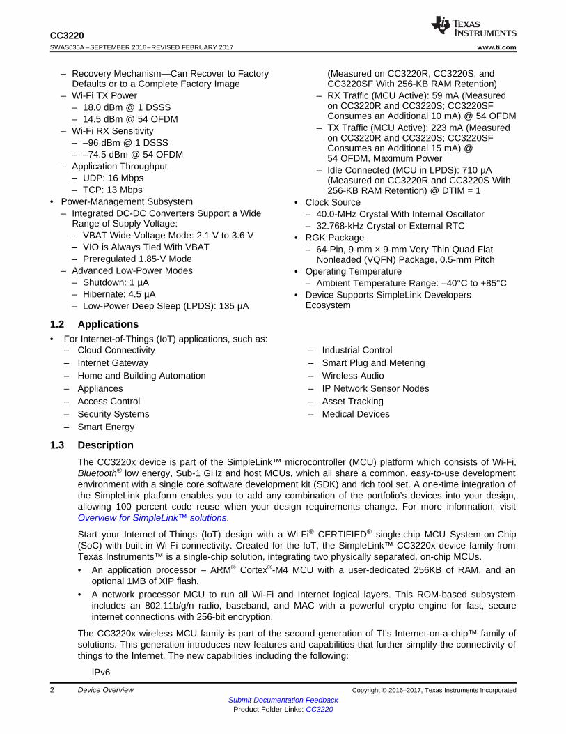
CC3220 SimpleLink™ Wi-Fi® Wireless and Internet-of-Things Solution,a Single-Chip Wireless MCU
1 Device Overview
1
1.1 Features1
• CC3220x SimpleLink™ Wi-Fi® WirelessMicrocontroller Unit (MCU) System-on-Chip (SoC)is a Single-Chip With Two Separate ExecutionEnvironments: a User Application Dedicated ARM®
Cortex®-M4 MCU and a Network Processor MCUto Run All Wi-Fi and Internet Logical Layers
• Chip-Level, Wi-Fi Alliance Wi-Fi CERTIFIED™• Applications Microcontroller Subsystem
– ARM® Cortex®-M4 Core at 80 MHz– Embedded Memory
– The CC3220R and CC3220S VariantsInclude 256KB of RAM
– The CC3220SF Variant is a Flash-BasedWireless MCU With Integrated 1MB of Flashand 256KB of RAM
– External Serial Flash– McASP Supports Two I2S Channels– SD– SPI– I2C– UART– 8-Bit Parallel Camera– Four General-Purpose Timers With 16-Bit PWM
Mode– Watchdog Timer– 4-Channel 12-Bit ADCs– Up to 27 GPIO Pins– Debug Interfaces: JTAG, cJTAG, SWD
• Wi-Fi Network Processor (NWP) Subsystem– Wi-Fi Internet-on-a-chip™ Dedicated ARM MCU
Completely Offloads Wi-Fi and InternetProtocols from the Application MCU
– Wi-Fi Modes:– 802.11b/g/n Station– 802.11b/g Access Point (AP) Supports up to
Four Stations– Wi-Fi Direct® Client and Group Owner
– WPA2 Personal and Enterprise Security: WEP,WPA/WPA2 PSK, WPA2 Enterprise (802.1x)
– IPv4 and IPv6 TCP/IP Stack– Industry-Standard BSD Socket Application
Programming Interfaces (APIs)– 16 Simultaneous TCP or UDP Sockets– 6 Simultaneous TLS and SSL Sockets
– IP Addressing: Static IP, LLA, DHCPv4,DHCPv6 With DAD
– SimpleLink Connection Manager forAutonomous and Fast Wi-Fi Connections
– Flexible Wi-Fi Provisioning With SmartConfig™Technology, AP Mode, and WPS2 Options
– RESTful API Support Using the Internal HTTPServer
– Embedded Network Applications Running onDedicated Network Processor
– Wide Set of Security Features:– Hardware Features:
– Separate Execution Environments– Device Identity– Hardware Crypto Engine for Advanced
Fast Security, Including: AES, DES,3DES, SHA2, MD5, CRC, and Checksum
– Initial Secure Programming:– Debug Security– JTAG and Debug Ports are Locked
– Personal and Enterprise Wi-Fi Security– Secure Sockets (SSLv3,
TLS1.0/1.1/TLS1.2)– Networking Security
– Personal and Enterprise Wi-Fi Security– Secure Sockets (SSLv3, TLS1.0, TLS1.1,
TLS1.2)– HTTPS Server– Trusted Root-Certificate Catalog– TI Root-of-Trust Public key
– SW IP Protection– Secure Key Storage– File System Security– Software Tamper Detection– Cloning Protection– Secure Boot: Validate the Integrity and
Authenticity of the Runtime Binary DuringBoot
– Embedded Network Applications Running on theDedicated Network Processor– HTTP/HTTPS Web Server With Dynamic
User Callbacks– mDNS, DNS-SD, DHCP Server– Ping
2
CC3220SWAS035A –SEPTEMBER 2016–REVISED FEBRUARY 2017 www.ti.com
Submit Documentation FeedbackProduct Folder Links: CC3220
Device Overview Copyright © 2016–2017, Texas Instruments Incorporated
– Recovery Mechanism—Can Recover to FactoryDefaults or to a Complete Factory Image
– Wi-Fi TX Power– 18.0 dBm @ 1 DSSS– 14.5 dBm @ 54 OFDM
– Wi-Fi RX Sensitivity– –96 dBm @ 1 DSSS– –74.5 dBm @ 54 OFDM
– Application Throughput– UDP: 16 Mbps– TCP: 13 Mbps
• Power-Management Subsystem– Integrated DC-DC Converters Support a Wide
Range of Supply Voltage:– VBAT Wide-Voltage Mode: 2.1 V to 3.6 V– VIO is Always Tied With VBAT– Preregulated 1.85-V Mode
– Advanced Low-Power Modes– Shutdown: 1 µA– Hibernate: 4.5 µA– Low-Power Deep Sleep (LPDS): 135 µA
(Measured on CC3220R, CC3220S, andCC3220SF With 256-KB RAM Retention)
– RX Traffic (MCU Active): 59 mA (Measuredon CC3220R and CC3220S; CC3220SFConsumes an Additional 10 mA) @ 54 OFDM
– TX Traffic (MCU Active): 223 mA (Measuredon CC3220R and CC3220S; CC3220SFConsumes an Additional 15 mA) @54 OFDM, Maximum Power
– Idle Connected (MCU in LPDS): 710 µA(Measured on CC3220R and CC3220S With256-KB RAM Retention) @ DTIM = 1
• Clock Source– 40.0-MHz Crystal With Internal Oscillator– 32.768-kHz Crystal or External RTC
• RGK Package– 64-Pin, 9-mm × 9-mm Very Thin Quad Flat
Nonleaded (VQFN) Package, 0.5-mm Pitch• Operating Temperature
– Ambient Temperature Range: –40°C to +85°C• Device Supports SimpleLink Developers
Ecosystem
1.2 Applications• For Internet-of-Things (IoT) applications, such as:
– Cloud Connectivity– Internet Gateway– Home and Building Automation– Appliances– Access Control– Security Systems– Smart Energy
– Industrial Control– Smart Plug and Metering– Wireless Audio– IP Network Sensor Nodes– Asset Tracking– Medical Devices
1.3 DescriptionThe CC3220x device is part of the SimpleLink™ microcontroller (MCU) platform which consists of Wi-Fi,Bluetooth® low energy, Sub-1 GHz and host MCUs, which all share a common, easy-to-use developmentenvironment with a single core software development kit (SDK) and rich tool set. A one-time integration ofthe SimpleLink platform enables you to add any combination of the portfolio’s devices into your design,allowing 100 percent code reuse when your design requirements change. For more information, visitOverview for SimpleLink™ solutions.
Start your Internet-of-Things (IoT) design with a Wi-Fi® CERTIFIED® single-chip MCU System-on-Chip(SoC) with built-in Wi-Fi connectivity. Created for the IoT, the SimpleLink™ CC3220x device family fromTexas Instruments™ is a single-chip solution, integrating two physically separated, on-chip MCUs.• An application processor – ARM® Cortex®-M4 MCU with a user-dedicated 256KB of RAM, and an
optional 1MB of XIP flash.• A network processor MCU to run all Wi-Fi and Internet logical layers. This ROM-based subsystem
includes an 802.11b/g/n radio, baseband, and MAC with a powerful crypto engine for fast, secureinternet connections with 256-bit encryption.
The CC3220x wireless MCU family is part of the second generation of TI’s Internet-on-a-chip™ family ofsolutions. This generation introduces new features and capabilities that further simplify the connectivity ofthings to the Internet. The new capabilities including the following:
IPv6
3
CC3220www.ti.com SWAS035A –SEPTEMBER 2016–REVISED FEBRUARY 2017
Submit Documentation FeedbackProduct Folder Links: CC3220
Device OverviewCopyright © 2016–2017, Texas Instruments Incorporated
Enhanced Wi-Fi provisioningEnhanced power consumptionEnhanced file system security (supported only by the CC3220S and CC3220SF devices)Wi-Fi AP connection with up to four stationsMore concurrently opened BSD sockets; up to 16 BSD sockets, of which 6 are secureHTTPS supportRESTful API supportAsymmetric keys crypto library
The CC3220x wireless MCU family supports the following modes: station, AP, and Wi-Fi Direct®. Thedevice also supports WPA2 personal and enterprise security. This subsystem includes embedded TCP/IPand TLS/SSL stacks, HTTP server, and multiple Internet protocols. The device supports a variety of Wi-Fiprovisioning methods including HTTP based on AP mode, SmartConfig™ Technology, and WPS2.0.
The power-management subsystem includes integrated DC-DC converters that support a wide range ofsupply voltages. This subsystem enables low-power consumption modes for extended battery life, such aslow-power deep sleep, hibernate with RTC (consuming only 4.5 µA), and shutdown mode (consuming only1 µA).
The device includes a wide variety of peripherals, including a fast parallel camera interface, I2S, SD,UART, SPI, I2C, and 4-channel ADC.
The SimpleLink CC3220x device family comes in three different device variants: CC3220R, CC3220S,and CC3220SF.
The CC3220R and CC3220S devices include 256KB of application-dedicated embedded RAM for codeand data, ROM with external serial flash bootloader, and peripheral drivers.
The CC3220SF device includes application-dedicated 1MB of XIP flash and 256KB of RAM for code anddata, ROM with external serial flash bootloader, and peripheral drivers. The CC3220S and CC3220SFdevice options have additional security features, such as encrypted and authenticated file systems, userIP encryption and authentication, secured boot (authentication and integrity validation of the applicationimage at flash and boot time), and more.
The CC3220x device family is a complete platform solution including software, sample applications, tools,user and programming guides, reference designs, and the E2E™ online community. The device family isalso part of the SimpleLink MCU portfolio and supports the SimpleLink developers ecosystem.
(1) For all available packages, see the orderable addendum at the end of the data sheet.
Device Information (1)
PART NUMBER PACKAGE BODY SIZECC3220RM2ARGKR/T VQFN (64) 9.00 mm × 9.00 mmCC3220SM2ARGKR/T VQFN (64) 9.00 mm × 9.00 mmCC3220SF12ARGKR/T VQFN (64) 9.00 mm × 9.00 mm
User Application
ARM® Cortex®-M4 80-MHz Processor
Internet Protocols
TLS/SSL
TCP/IP
ARM Processor (Wi-Fi Network Processor)
Embedded Internet
Embedded Wi-Fi®
Supplicant
Wi-Fi Driver
Wi-Fi Baseband
Wi-Fi MAC
Wi-Fi Radio
Copyright © 2017, Texas Instruments Incorporated
Pow
erM
anag
emen
tS
yste
mP
eripheral InterfacesA
nalog
Network Processor
RAM
ROM
ARM® Cortex®-M4
80 MHz
JTAG
DC-DC
Hibernate RTC
ADC
PWM
Camera
SPI
UART
I2C
SD
I2S/PCMOscillators
Timers
GPIOs
DMA
Copyright © 2017, Texas Instruments Incorporated
4
CC3220SWAS035A –SEPTEMBER 2016–REVISED FEBRUARY 2017 www.ti.com
Submit Documentation FeedbackProduct Folder Links: CC3220
Device Overview Copyright © 2016–2017, Texas Instruments Incorporated
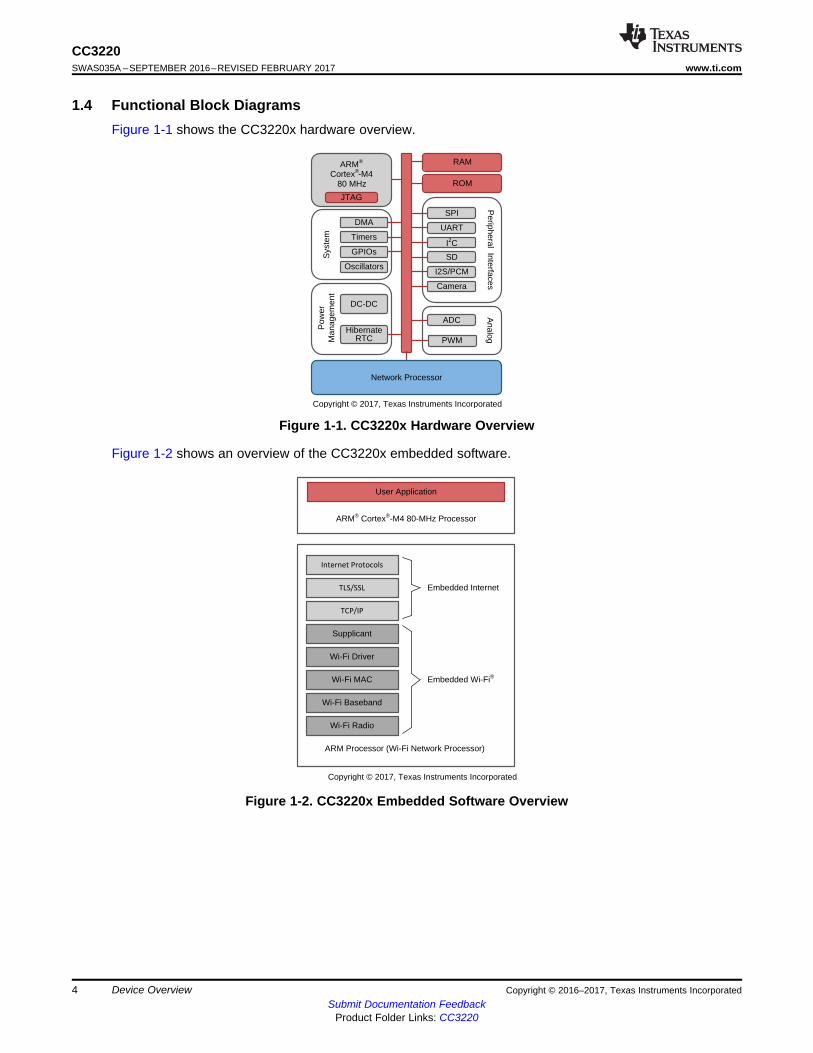
1.4 Functional Block DiagramsFigure 1-1 shows the CC3220x hardware overview.
Figure 1-1. CC3220x Hardware Overview
Figure 1-2 shows an overview of the CC3220x embedded software.
Figure 1-2. CC3220x Embedded Software Overview
5
CC3220www.ti.com SWAS035A –SEPTEMBER 2016–REVISED FEBRUARY 2017
Submit Documentation FeedbackProduct Folder Links: CC3220
Revision HistoryCopyright © 2016–2017, Texas Instruments Incorporated
Table of Contents1 Device Overview ......................................... 1
1.1 Features .............................................. 11.2 Applications........................................... 21.3 Description............................................ 21.4 Functional Block Diagrams ........................... 4
2 Revision History ......................................... 53 Terminal Configuration and Functions.............. 6
3.1 Pin Diagram .......................................... 63.2 Pin Attributes and Pin Multiplexing ................... 73.3 Drive Strength and Reset States for Analog and
Digital Multiplexed Pins ............................. 233.4 Pad State After Application of Power To Chip But
Before Reset Release............................... 233.5 Connections for Unused Pins ....................... 24
4 Specifications ........................................... 254.1 Absolute Maximum Ratings ......................... 254.2 ESD Ratings ........................................ 254.3 Power-On Hours .................................... 254.4 Recommended Operating Conditions............... 254.5 Current Consumption Summary (CC3220R,
CC3220S) ........................................... 264.6 Current Consumption Summary (CC3200SF) ...... 274.7 TX Power and IBAT versus TX Power Level
Settings.............................................. 284.8 Brownout and Blackout Conditions ................. 304.9 Electrical Characteristics (3.3 V, 25°C) ............. 314.10 WLAN Receiver Characteristics .................... 334.11 WLAN Transmitter Characteristics .................. 334.12 WLAN Filter Requirements.......................... 34
4.13 Thermal Resistance Characteristics for RGKPackage ............................................. 34
4.14 Timing and Switching Characteristics ............... 345 Detailed Description ................................... 51
5.1 Overview ............................................ 515.2 Functional Block Diagram........................... 515.3 ARM® Cortex®-M4 Processor Core Subsystem .... 525.4 Wi-Fi Network Processor Subsystem ............... 525.5 Security.............................................. 555.6 Power-Management Subsystem .................... 585.7 Low-Power Operating Mode ........................ 595.8 Memory.............................................. 615.9 Restoring Factory Default Configuration ............ 645.10 Boot Modes.......................................... 64
6 Applications, Implementation, and Layout........ 666.1 Application Information .............................. 666.2 PCB Layout Guidelines ............................. 71
7 Device and Documentation Support ............... 747.1 Tools and Software ................................. 747.2 Device Nomenclature ............................... 757.3 Documentation Support ............................. 757.4 Community Resources .............................. 777.5 Trademarks.......................................... 787.6 Electrostatic Discharge Caution..................... 787.7 Export Control Notice ............................... 787.8 Glossary ............................................. 78
8 Mechanical, Packaging, and OrderableInformation .............................................. 79
2 Revision HistoryNOTE: Page numbers for previous revisions may differ from page numbers in the current version.
Changes from September 28, 2016 to February 8, 2017 Page
• Changed the orderable part numbers in Device Information table ............................................................. 3• Changed RF pins UNIT to dB ..................................................................................................... 25• Added test conditions to VOH and VOL rows of Section 4.9 .................................................................... 31• Changed "timing parameters" to "electrical specifications" .................................................................... 47• Changed note from "Corrected through firmware" to "Offset error < 1 LSB. TI recommends using the ADC API
functions, which automatically compensate for offset error." .................................................................. 47• Added note on GPIO_26 and GPIO_27.......................................................................................... 67• Added Table 6-1 .................................................................................................................... 68• Added Figure 6-2.................................................................................................................... 69• Added Table 6-2 .................................................................................................................... 70
VDD_RAM
GPIO0
RTC_XTAL_P
RTC_XTAL_N
GPIO30
VIN_IO2
GPIO1
VDD_DIG2
GPIO2
GPIO3
GPIO4
GPIO5
GPIO6
GPIO7
GPIO8
GPIO9
49
50
51
52
53
54
55
56
57
58
59
60
61
62
63
64
48 47 46 45 44 43 42 41 40 39 38 37 36 35 34 33
VD
D_A
NA
1
VD
D_A
NA
2
DC
DC
_AN
A2_
SW
_N
DC
DC
_AN
A2_
SW
_P
VIN
_DC
DC
_DIG
DC
DC
_DIG
_SW
DC
DC
_PA
_OU
T
DC
DC
_PA
_SW
_N
DC
DC
_PA
_SW
_P
VIN
_DC
DC
_PA
DC
DC
_AN
A_S
W
VIN
_DC
DC
_AN
A
LDO
_IN
1
SO
P0
SO
P1
VD
D_P
A_I
N
32
31
30
29
28
27
26
25
24
23
22
21
20
19
18
17
nRESET
RF_BG
ANTSEL2
ANTSEL1
NC
NC
NC
LDO_IN2
VDD_PLL
WLAN_XTAL_P
WLAN_XTAL_N
SOP2
TMS
TCK
GPIO28
TDO
1 2 3 4 5 6 7 8 9 10 11 12 13 14 15 16
GP
IO10
GP
IO11
GP
IO12
GP
IO13
GP
IO14
GP
IO15
GP
IO16
GP
IO17
VD
D_D
IG1
VIN
_IO
1
FLA
SH
_SP
I_C
LK
FLA
SH
_SP
I_D
OU
T
FLA
SH
_SP
I_D
IN
FLA
SH
_SP
I_C
S
GP
IO22 TD
I
6
CC3220SWAS035A –SEPTEMBER 2016–REVISED FEBRUARY 2017 www.ti.com
Submit Documentation FeedbackProduct Folder Links: CC3220
Terminal Configuration and Functions Copyright © 2016–2017, Texas Instruments Incorporated
3 Terminal Configuration and Functions
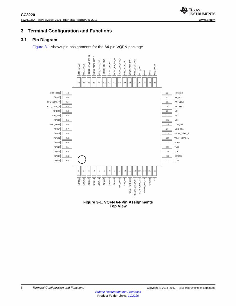
3.1 Pin DiagramFigure 3-1 shows pin assignments for the 64-pin VQFN package.
Figure 3-1. VQFN 64-Pin AssignmentsTop View
7
CC3220www.ti.com SWAS035A –SEPTEMBER 2016–REVISED FEBRUARY 2017
Submit Documentation FeedbackProduct Folder Links: CC3220
Terminal Configuration and FunctionsCopyright © 2016–2017, Texas Instruments Incorporated
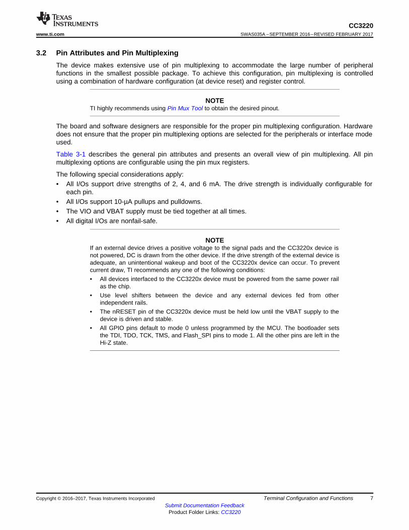
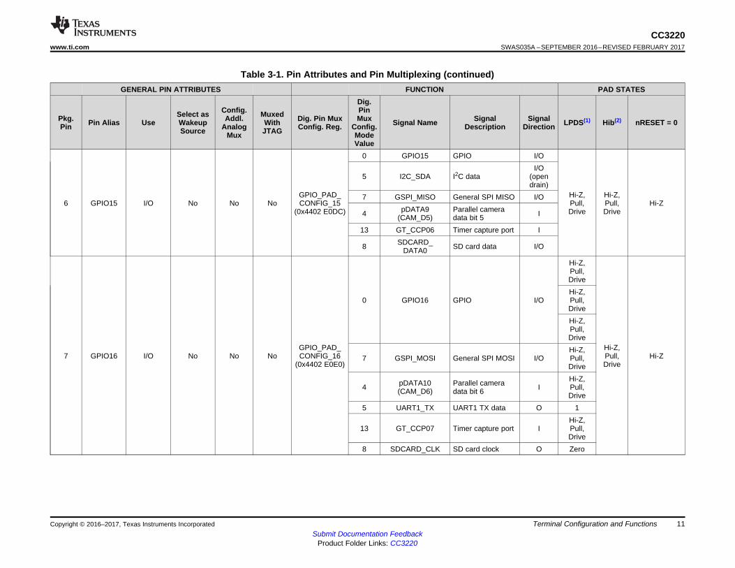
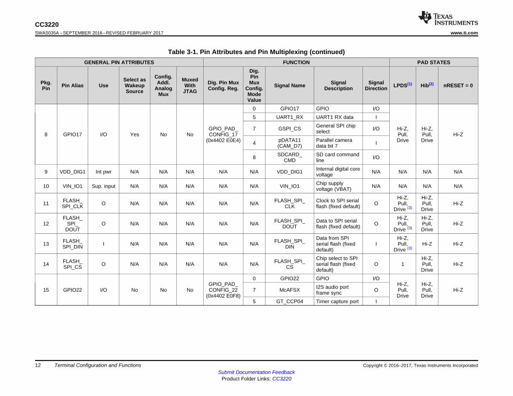
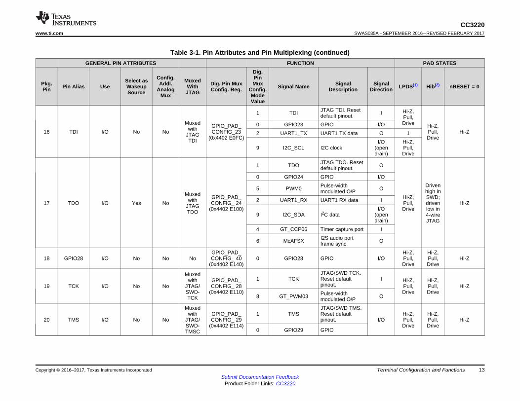
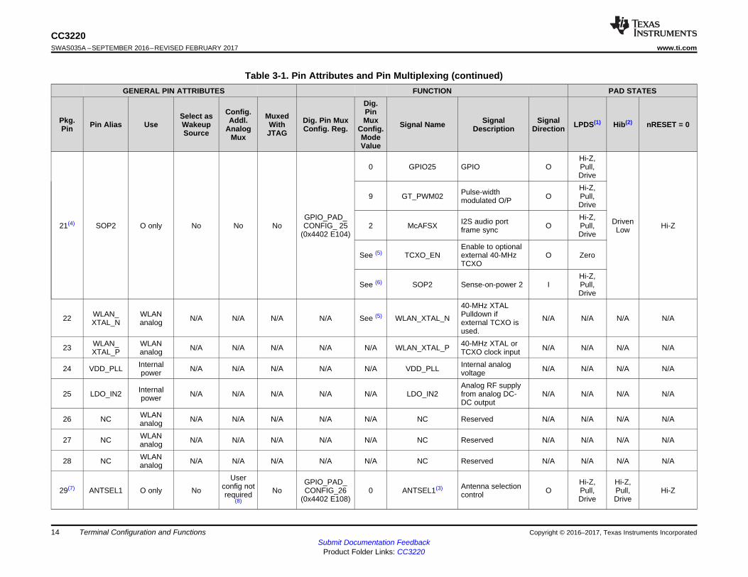
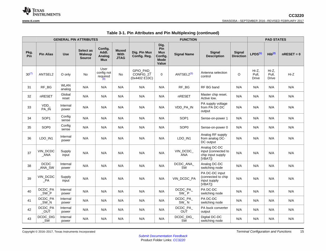
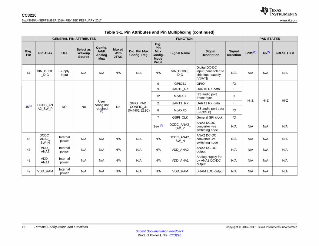
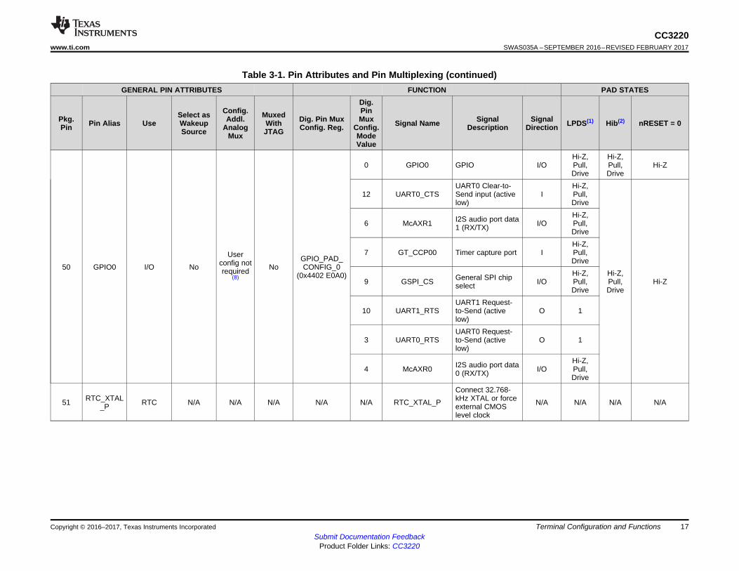
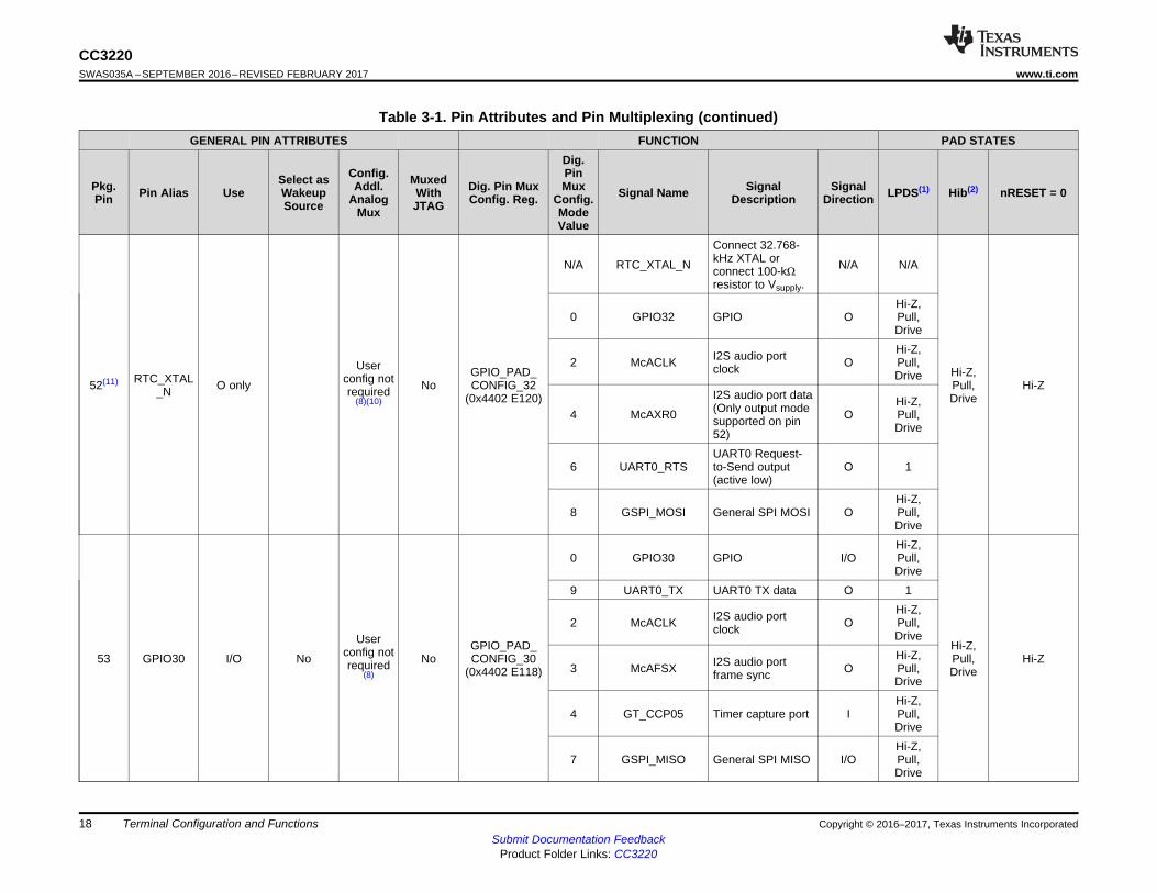
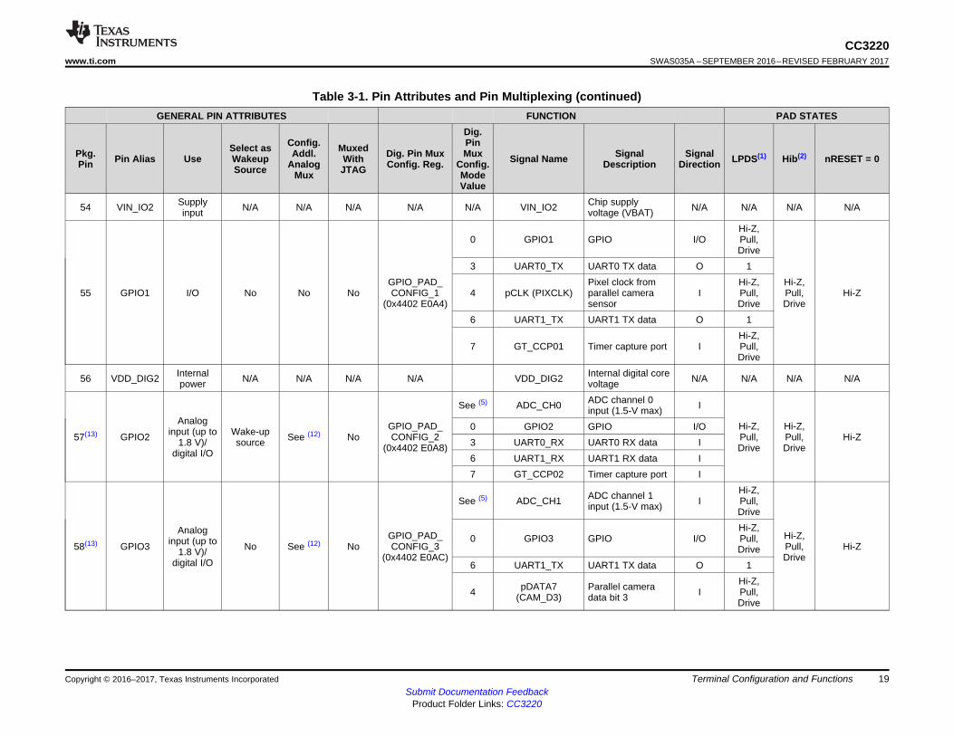
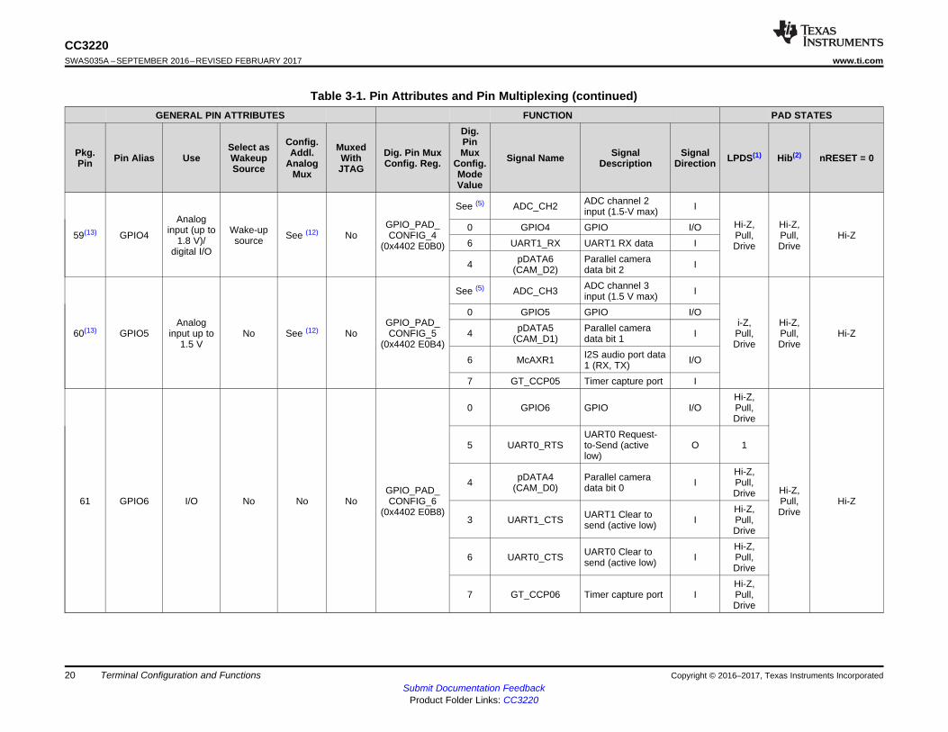
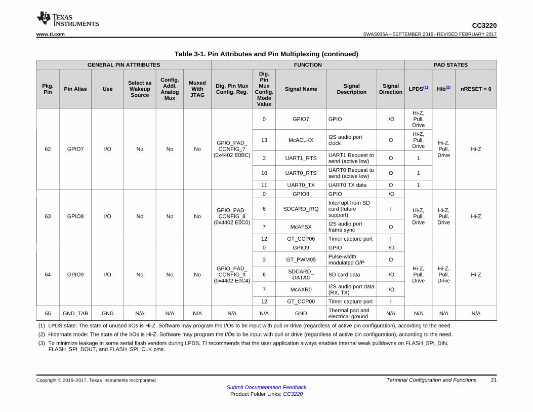
3.2 Pin Attributes and Pin MultiplexingThe device makes extensive use of pin multiplexing to accommodate the large number of peripheralfunctions in the smallest possible package. To achieve this configuration, pin multiplexing is controlledusing a combination of hardware configuration (at device reset) and register control.
NOTETI highly recommends using Pin Mux Tool to obtain the desired pinout.
The board and software designers are responsible for the proper pin multiplexing configuration. Hardwaredoes not ensure that the proper pin multiplexing options are selected for the peripherals or interface modeused.
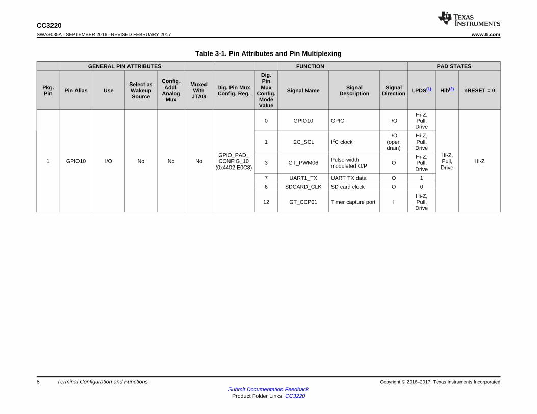
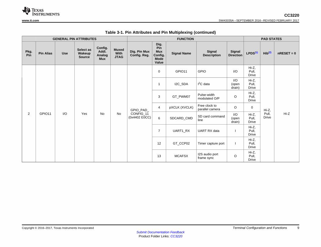
Table 3-1 describes the general pin attributes and presents an overall view of pin multiplexing. All pinmultiplexing options are configurable using the pin mux registers.
The following special considerations apply:• All I/Os support drive strengths of 2, 4, and 6 mA. The drive strength is individually configurable for
each pin.• All I/Os support 10-µA pullups and pulldowns.• The VIO and VBAT supply must be tied together at all times.• All digital I/Os are nonfail-safe.
NOTEIf an external device drives a positive voltage to the signal pads and the CC3220x device isnot powered, DC is drawn from the other device. If the drive strength of the external device isadequate, an unintentional wakeup and boot of the CC3220x device can occur. To preventcurrent draw, TI recommends any one of the following conditions:• All devices interfaced to the CC3220x device must be powered from the same power rail
as the chip.• Use level shifters between the device and any external devices fed from other
independent rails.• The nRESET pin of the CC3220x device must be held low until the VBAT supply to the
device is driven and stable.• All GPIO pins default to mode 0 unless programmed by the MCU. The bootloader sets
the TDI, TDO, TCK, TMS, and Flash_SPI pins to mode 1. All the other pins are left in theHi-Z state.
Copyright © 2016–2017, Texas Instruments IncorporatedTerminal Configuration and FunctionsSubmit Documentation Feedback
Product Folder Links: CC3220
8
CC3220SWAS035A –SEPTEMBER 2016–REVISED FEBRUARY 2017 www.ti.com
Table 3-1. Pin Attributes and Pin Multiplexing
GENERAL PIN ATTRIBUTES FUNCTION PAD STATES
Pkg.Pin Pin Alias Use
Select asWakeupSource
Config.Addl.
AnalogMux
MuxedWithJTAG
Dig. Pin MuxConfig. Reg.
Dig.PinMux
Config.ModeValue
Signal Name SignalDescription
SignalDirection LPDS(1) Hib(2) nRESET = 0
1 GPIO10 I/O No No NoGPIO_PAD_CONFIG_10
(0x4402 E0C8)
0 GPIO10 GPIO I/OHi-Z,Pull,Drive
Hi-Z,Pull,Drive
Hi-Z
1 I2C_SCL I2C clockI/O
(opendrain)
Hi-Z,Pull,Drive
3 GT_PWM06 Pulse-widthmodulated O/P O
Hi-Z,Pull,Drive
7 UART1_TX UART TX data O 16 SDCARD_CLK SD card clock O 0
12 GT_CCP01 Timer capture port IHi-Z,Pull,Drive
Copyright © 2016–2017, Texas Instruments Incorporated Terminal Configuration and FunctionsSubmit Documentation Feedback
Product Folder Links: CC3220
9
CC3220www.ti.com SWAS035A –SEPTEMBER 2016–REVISED FEBRUARY 2017
Table 3-1. Pin Attributes and Pin Multiplexing (continued)GENERAL PIN ATTRIBUTES FUNCTION PAD STATES
Pkg.Pin Pin Alias Use
Select asWakeupSource
Config.Addl.
AnalogMux
MuxedWithJTAG
Dig. Pin MuxConfig. Reg.
Dig.PinMux
Config.ModeValue
Signal Name SignalDescription
SignalDirection LPDS(1) Hib(2) nRESET = 0
2 GPIO11 I/O Yes No NoGPIO_PAD_CONFIG_11
(0x4402 E0CC)
0 GPIO11 GPIO I/OHi-Z,Pull,Drive
Hi-Z,Pull,Drive
Hi-Z
1 I2C_SDA I2C dataI/O
(opendrain)
Hi-Z,Pull,Drive
3 GT_PWM07 Pulse-widthmodulated O/P O
Hi-Z,Pull,Drive
4 pXCLK (XVCLK) Free clock toparallel camera O 0
6 SDCARD_CMD SD card commandline
I/O(opendrain)
Hi-Z,Pull,Drive
7 UART1_RX UART RX data IHi-Z,Pull,Drive
12 GT_CCP02 Timer capture port IHi-Z,Pull,Drive
13 MCAFSX I2S audio portframe sync O
Hi-Z,Pull,Drive
Copyright © 2016–2017, Texas Instruments IncorporatedTerminal Configuration and FunctionsSubmit Documentation Feedback
Product Folder Links: CC3220
10
CC3220SWAS035A –SEPTEMBER 2016–REVISED FEBRUARY 2017 www.ti.com
Table 3-1. Pin Attributes and Pin Multiplexing (continued)GENERAL PIN ATTRIBUTES FUNCTION PAD STATES
Pkg.Pin Pin Alias Use
Select asWakeupSource
Config.Addl.
AnalogMux
MuxedWithJTAG
Dig. Pin MuxConfig. Reg.
Dig.PinMux
Config.ModeValue
Signal Name SignalDescription
SignalDirection LPDS(1) Hib(2) nRESET = 0
3 GPIO12 I/O No No NoGPIO_PAD_CONFIG_12
(0x4402 E0D0)
0 GPIO12 GPIO I/OHi-Z,Pull,Drive
Hi-Z,Pull,Drive
Hi-Z
3 McACLK I2S audio portclock output O
Hi-Z,Pull,Drive
4 pVS (VSYNC) Parallel cameravertical sync I
Hi-Z,Pull,Drive
5 I2C_SCL I2C clockI/O
(opendrain)
Hi-Z,Pull,Drive
7 UART0_TX UART0 TX data O 1
12 GT_CCP03 Timer capture port IHi-Z,Pull,Drive
4 GPIO13 I/O Yes No NoGPIO_PAD_CONFIG_13
(0x4402 E0D4)
0 GPIO13 GPIO I/O
Hi-Z,Pull,Drive
Hi-Z,Pull,Drive
Hi-Z
5 I2C_SDA I2C dataI/O
(opendrain)
4 pHS (HSYNC) Parallel camerahorizontal sync I
7 UART0_RX UART0 RX data I12 GT_CCP04 Timer capture port I
5 GPIO14 I/O No No NoGPIO_PAD_CONFIG_14
(0x4402 E0D8)
0 GPIO14 GPIO I/O
Hi-Z,Pull,Drive
Hi-Z,Pull,Drive
Hi-Z
5 I2C_SCL I2C clockI/O
(opendrain)
7 GSPI_CLK General SPI clock I/O
4 pDATA8(CAM_D4)
Parallel cameradata bit 4 I
12 GT_CCP05 Timer capture port I
Copyright © 2016–2017, Texas Instruments Incorporated Terminal Configuration and FunctionsSubmit Documentation Feedback
Product Folder Links: CC3220
11
CC3220www.ti.com SWAS035A –SEPTEMBER 2016–REVISED FEBRUARY 2017
Table 3-1. Pin Attributes and Pin Multiplexing (continued)GENERAL PIN ATTRIBUTES FUNCTION PAD STATES
Pkg.Pin Pin Alias Use
Select asWakeupSource
Config.Addl.
AnalogMux
MuxedWithJTAG
Dig. Pin MuxConfig. Reg.
Dig.PinMux
Config.ModeValue
Signal Name SignalDescription
SignalDirection LPDS(1) Hib(2) nRESET = 0
6 GPIO15 I/O No No NoGPIO_PAD_CONFIG_15
(0x4402 E0DC)
0 GPIO15 GPIO I/O
Hi-Z,Pull,Drive
Hi-Z,Pull,Drive
Hi-Z
5 I2C_SDA I2C dataI/O
(opendrain)
7 GSPI_MISO General SPI MISO I/O
4 pDATA9(CAM_D5)
Parallel cameradata bit 5 I
13 GT_CCP06 Timer capture port I
8 SDCARD_DATA0 SD card data I/O
7 GPIO16 I/O No No NoGPIO_PAD_CONFIG_16
(0x4402 E0E0)
0 GPIO16 GPIO I/O
Hi-Z,Pull,Drive
Hi-Z,Pull,Drive
Hi-Z
Hi-Z,Pull,DriveHi-Z,Pull,Drive
7 GSPI_MOSI General SPI MOSI I/OHi-Z,Pull,Drive
4 pDATA10(CAM_D6)
Parallel cameradata bit 6 I
Hi-Z,Pull,Drive
5 UART1_TX UART1 TX data O 1
13 GT_CCP07 Timer capture port IHi-Z,Pull,Drive
8 SDCARD_CLK SD card clock O Zero
Copyright © 2016–2017, Texas Instruments IncorporatedTerminal Configuration and FunctionsSubmit Documentation Feedback
Product Folder Links: CC3220
12
CC3220SWAS035A –SEPTEMBER 2016–REVISED FEBRUARY 2017 www.ti.com
Table 3-1. Pin Attributes and Pin Multiplexing (continued)GENERAL PIN ATTRIBUTES FUNCTION PAD STATES
Pkg.Pin Pin Alias Use
Select asWakeupSource
Config.Addl.
AnalogMux
MuxedWithJTAG
Dig. Pin MuxConfig. Reg.
Dig.PinMux
Config.ModeValue
Signal Name SignalDescription
SignalDirection LPDS(1) Hib(2) nRESET = 0
8 GPIO17 I/O Yes No NoGPIO_PAD_CONFIG_17
(0x4402 E0E4)
0 GPIO17 GPIO I/O
Hi-Z,Pull,Drive
Hi-Z,Pull,Drive
Hi-Z
5 UART1_RX UART1 RX data I
7 GSPI_CS General SPI chipselect I/O
4 pDATA11(CAM_D7)
Parallel cameradata bit 7 I
8 SDCARD_CMD
SD card commandline I/O
9 VDD_DIG1 Int pwr N/A N/A N/A N/A N/A VDD_DIG1 Internal digital corevoltage N/A N/A N/A N/A
10 VIN_IO1 Sup. input N/A N/A N/A N/A N/A VIN_IO1 Chip supplyvoltage (VBAT) N/A N/A N/A N/A
11 FLASH_SPI_CLK O N/A N/A N/A N/A N/A FLASH_SPI_
CLKClock to SPI serialflash (fixed default) O
Hi-Z,Pull,
Drive (3)
Hi-Z,Pull,Drive
Hi-Z
12FLASH_
SPI_DOUT
O N/A N/A N/A N/A N/A FLASH_SPI_DOUT
Data to SPI serialflash (fixed default) O
Hi-Z,Pull,
Drive (3)
Hi-Z,Pull,Drive
Hi-Z
13 FLASH_SPI_DIN I N/A N/A N/A N/A N/A FLASH_SPI_
DIN
Data from SPIserial flash (fixeddefault)
IHi-Z,Pull,
Drive (3)Hi-Z Hi-Z
14 FLASH_SPI_CS O N/A N/A N/A N/A N/A FLASH_SPI_
CS
Chip select to SPIserial flash (fixeddefault)
O 1Hi-Z,Pull,Drive
Hi-Z
15 GPIO22 I/O No No NoGPIO_PAD_CONFIG_22
(0x4402 E0F8)
0 GPIO22 GPIO I/OHi-Z,Pull,Drive
Hi-Z,Pull,Drive
Hi-Z7 McAFSX I2S audio portframe sync O
5 GT_CCP04 Timer capture port I
Copyright © 2016–2017, Texas Instruments Incorporated Terminal Configuration and FunctionsSubmit Documentation Feedback
Product Folder Links: CC3220
13
CC3220www.ti.com SWAS035A –SEPTEMBER 2016–REVISED FEBRUARY 2017
Table 3-1. Pin Attributes and Pin Multiplexing (continued)GENERAL PIN ATTRIBUTES FUNCTION PAD STATES
Pkg.Pin Pin Alias Use
Select asWakeupSource
Config.Addl.
AnalogMux
MuxedWithJTAG
Dig. Pin MuxConfig. Reg.
Dig.PinMux
Config.ModeValue
Signal Name SignalDescription
SignalDirection LPDS(1) Hib(2) nRESET = 0
16 TDI I/O No No
Muxedwith
JTAGTDI
GPIO_PAD_CONFIG_23
(0x4402 E0FC)
1 TDI JTAG TDI. Resetdefault pinout. I Hi-Z,
Pull,Drive Hi-Z,
Pull,Drive
Hi-Z0 GPIO23 GPIO I/O2 UART1_TX UART1 TX data O 1
9 I2C_SCL I2C clockI/O
(opendrain)
Hi-Z,Pull,Drive
17 TDO I/O Yes No
Muxedwith
JTAGTDO
GPIO_PAD_CONFIG_ 24
(0x4402 E100)
1 TDO JTAG TDO. Resetdefault pinout. O
Hi-Z,Pull,Drive
Drivenhigh inSWD;drivenlow in4-wireJTAG
Hi-Z
0 GPIO24 GPIO I/O
5 PWM0 Pulse-widthmodulated O/P O
2 UART1_RX UART1 RX data I
9 I2C_SDA I2C dataI/O
(opendrain)
4 GT_CCP06 Timer capture port I
6 McAFSX I2S audio portframe sync O
18 GPIO28 I/O No No NoGPIO_PAD_CONFIG_ 40
(0x4402 E140)0 GPIO28 GPIO I/O
Hi-Z,Pull,Drive
Hi-Z,Pull,Drive
Hi-Z
19 TCK I/O No No
Muxedwith
JTAG/SWD-TCK
GPIO_PAD_CONFIG_ 28
(0x4402 E110)
1 TCKJTAG/SWD TCK.Reset defaultpinout.
I Hi-Z,Pull,Drive
Hi-Z,Pull,Drive
Hi-Z
8 GT_PWM03 Pulse-widthmodulated O/P O
20 TMS I/O No No
Muxedwith
JTAG/SWD-TMSC
GPIO_PAD_CONFIG_ 29
(0x4402 E114)
1 TMSJTAG/SWD TMS.Reset defaultpinout. I/O
Hi-Z,Pull,Drive
Hi-Z,Pull,Drive
Hi-Z
0 GPIO29 GPIO
Copyright © 2016–2017, Texas Instruments IncorporatedTerminal Configuration and FunctionsSubmit Documentation Feedback
Product Folder Links: CC3220
14
CC3220SWAS035A –SEPTEMBER 2016–REVISED FEBRUARY 2017 www.ti.com
Table 3-1. Pin Attributes and Pin Multiplexing (continued)GENERAL PIN ATTRIBUTES FUNCTION PAD STATES
Pkg.Pin Pin Alias Use
Select asWakeupSource
Config.Addl.
AnalogMux
MuxedWithJTAG
Dig. Pin MuxConfig. Reg.
Dig.PinMux
Config.ModeValue
Signal Name SignalDescription
SignalDirection LPDS(1) Hib(2) nRESET = 0
21(4) SOP2 O only No No NoGPIO_PAD_CONFIG_ 25
(0x4402 E104)
0 GPIO25 GPIO OHi-Z,Pull,Drive
DrivenLow Hi-Z
9 GT_PWM02 Pulse-widthmodulated O/P O
Hi-Z,Pull,Drive
2 McAFSX I2S audio portframe sync O
Hi-Z,Pull,Drive
See (5) TCXO_ENEnable to optionalexternal 40-MHzTCXO
O Zero
See (6) SOP2 Sense-on-power 2 IHi-Z,Pull,Drive
22 WLAN_XTAL_N
WLANanalog N/A N/A N/A N/A See (5) WLAN_XTAL_N
40-MHz XTALPulldown ifexternal TCXO isused.
N/A N/A N/A N/A
23 WLAN_XTAL_P
WLANanalog N/A N/A N/A N/A N/A WLAN_XTAL_P 40-MHz XTAL or
TCXO clock input N/A N/A N/A N/A
24 VDD_PLL Internalpower N/A N/A N/A N/A N/A VDD_PLL Internal analog
voltage N/A N/A N/A N/A
25 LDO_IN2 Internalpower N/A N/A N/A N/A N/A LDO_IN2
Analog RF supplyfrom analog DC-DC output
N/A N/A N/A N/A
26 NC WLANanalog N/A N/A N/A N/A N/A NC Reserved N/A N/A N/A N/A
27 NC WLANanalog N/A N/A N/A N/A N/A NC Reserved N/A N/A N/A N/A
28 NC WLANanalog N/A N/A N/A N/A N/A NC Reserved N/A N/A N/A N/A
29(7) ANTSEL1 O only No
Userconfig notrequired
(8)
NoGPIO_PAD_CONFIG_26
(0x4402 E108)0 ANTSEL1(3) Antenna selection
control OHi-Z,Pull,Drive
Hi-Z,Pull,Drive
Hi-Z
Copyright © 2016–2017, Texas Instruments Incorporated Terminal Configuration and FunctionsSubmit Documentation Feedback
Product Folder Links: CC3220
15
CC3220www.ti.com SWAS035A –SEPTEMBER 2016–REVISED FEBRUARY 2017
Table 3-1. Pin Attributes and Pin Multiplexing (continued)GENERAL PIN ATTRIBUTES FUNCTION PAD STATES
Pkg.Pin Pin Alias Use
Select asWakeupSource
Config.Addl.
AnalogMux
MuxedWithJTAG
Dig. Pin MuxConfig. Reg.
Dig.PinMux
Config.ModeValue
Signal Name SignalDescription
SignalDirection LPDS(1) Hib(2) nRESET = 0
30(7) ANTSEL2 O only No
Userconfig notrequired
(8)
NoGPIO_PAD_CONFIG_27
(0x4402 E10C)0 ANTSEL2(3) Antenna selection
control OHi-Z,Pull,Drive
Hi-Z,Pull,Drive
Hi-Z
31 RF_BG WLANanalog N/A N/A N/A N/A N/A RF_BG RF BG band N/A N/A N/A N/A
32 nRESET Globalreset N/A N/A N/A N/A N/A nRESET Master chip reset.
Active low. N/A N/A N/A N/A
33 VDD_PA_IN
Internalpower N/A N/A N/A N/A N/A VDD_PA_IN
PA supply voltagefrom PA DC-DCoutput
N/A N/A N/A N/A
34 SOP1 Configsense N/A N/A N/A N/A N/A SOP1 Sense-on-power 1 N/A N/A N/A N/A
35 SOP0 Configsense N/A N/A N/A N/A N/A SOP0 Sense-on-power 0 N/A N/A N/A N/A
36 LDO_IN1 Internalpower N/A N/A N/A N/A N/A LDO_IN1
Analog RF supplyfrom analog DC-DC output
N/A N/A N/A N/A
37 VIN_DCDC_ANA
Supplyinput N/A N/A N/A N/A N/A VIN_DCDC_
ANA
Analog DC-DCinput (connected tochip input supply[VBAT])
N/A N/A N/A N/A
38 DCDC_ANA_SW
Internalpower N/A N/A N/A N/A N/A DCDC_ANA_
SWAnalog DC-DCswitching node N/A N/A N/A N/A
39 VIN_DCDC_PA
Supplyinput N/A N/A N/A N/A N/A VIN_DCDC_PA
PA DC-DC input(connected to chipinput supply[VBAT])
N/A N/A N/A N/A
40 DCDC_PA_SW_P
Internalpower N/A N/A N/A N/A N/A DCDC_PA_
SW_ PPA DC-DCswitching node N/A N/A N/A N/A
41 DCDC_PA_SW_N
Internalpower N/A N/A N/A N/A N/A DCDC_PA_
SW_ NPA DC-DCswitching node N/A N/A N/A N/A
42 DCDC_PA_OUT
Internalpower N/A N/A N/A N/A N/A DCDC_PA_
OUTPA buck converteroutput N/A N/A N/A N/A
43 DCDC_DIG_SW
Internalpower N/A N/A N/A N/A N/A DCDC_DIG_
SWDigital DC-DCswitching node N/A N/A N/A N/A
Copyright © 2016–2017, Texas Instruments IncorporatedTerminal Configuration and FunctionsSubmit Documentation Feedback
Product Folder Links: CC3220
16
CC3220SWAS035A –SEPTEMBER 2016–REVISED FEBRUARY 2017 www.ti.com
Table 3-1. Pin Attributes and Pin Multiplexing (continued)GENERAL PIN ATTRIBUTES FUNCTION PAD STATES
Pkg.Pin Pin Alias Use
Select asWakeupSource
Config.Addl.
AnalogMux
MuxedWithJTAG
Dig. Pin MuxConfig. Reg.
Dig.PinMux
Config.ModeValue
Signal Name SignalDescription
SignalDirection LPDS(1) Hib(2) nRESET = 0
44 VIN_DCDC_DIG
Supplyinput N/A N/A N/A N/A N/A VIN_DCDC_
DIG
Digital DC-DCinput (connected tochip input supply[VBAT])
N/A N/A N/A N/A
45(9) DCDC_ANA2_SW_P I/O No
Userconfig notrequired
(8)
NoGPIO_PAD_CONFIG_31
(0x4402 E11C)
0 GPIO31 GPIO I/O
Hi-Z Hi-Z Hi-Z
9 UART0_RX UART0 RX data I
12 McAFSX I2S audio portframe sync O
2 UART1_RX UART1 RX data I
6 McAXR0 I2S audio port data0 (RX/TX) I/O
7 GSPI_CLK General SPI clock I/O
See (5) DCDC_ANA2_SW_P
ANA2 DCDCconverter +veswitching node
N/A N/A N/A N/A
46DCDC_ANA2_SW_N
Internalpower N/A N/A N/A N/A N/A DCDC_ANA2_
SW_N
ANA2 DC-DCconverter -veswitching node
N/A N/A N/A N/A
47 VDD_ANA2
Internalpower N/A N/A N/A N/A N/A VDD_ANA2 ANA2 DC-DC
output N/A N/A N/A N/A
48 VDD_ANA1
Internalpower N/A N/A N/A N/A N/A VDD_ANA1
Analog supply fedby ANA2 DC-DCoutput
N/A N/A N/A N/A
49 VDD_RAM Internalpower N/A N/A N/A N/A N/A VDD_RAM SRAM LDO output N/A N/A N/A N/A
Copyright © 2016–2017, Texas Instruments Incorporated Terminal Configuration and FunctionsSubmit Documentation Feedback
Product Folder Links: CC3220
17
CC3220www.ti.com SWAS035A –SEPTEMBER 2016–REVISED FEBRUARY 2017
Table 3-1. Pin Attributes and Pin Multiplexing (continued)GENERAL PIN ATTRIBUTES FUNCTION PAD STATES
Pkg.Pin Pin Alias Use
Select asWakeupSource
Config.Addl.
AnalogMux
MuxedWithJTAG
Dig. Pin MuxConfig. Reg.
Dig.PinMux
Config.ModeValue
Signal Name SignalDescription
SignalDirection LPDS(1) Hib(2) nRESET = 0
50 GPIO0 I/O No
Userconfig notrequired
(8)
NoGPIO_PAD_CONFIG_0
(0x4402 E0A0)
0 GPIO0 GPIO I/OHi-Z,Pull,Drive
Hi-Z,Pull,Drive
Hi-Z
12 UART0_CTSUART0 Clear-to-Send input (activelow)
IHi-Z,Pull,Drive
Hi-Z,Pull,Drive
Hi-Z
6 McAXR1 I2S audio port data1 (RX/TX) I/O
Hi-Z,Pull,Drive
7 GT_CCP00 Timer capture port IHi-Z,Pull,Drive
9 GSPI_CS General SPI chipselect I/O
Hi-Z,Pull,Drive
10 UART1_RTSUART1 Request-to-Send (activelow)
O 1
3 UART0_RTSUART0 Request-to-Send (activelow)
O 1
4 McAXR0 I2S audio port data0 (RX/TX) I/O
Hi-Z,Pull,Drive
51 RTC_XTAL_P RTC N/A N/A N/A N/A N/A RTC_XTAL_P
Connect 32.768-kHz XTAL or forceexternal CMOSlevel clock
N/A N/A N/A N/A
Copyright © 2016–2017, Texas Instruments IncorporatedTerminal Configuration and FunctionsSubmit Documentation Feedback
Product Folder Links: CC3220
18
CC3220SWAS035A –SEPTEMBER 2016–REVISED FEBRUARY 2017 www.ti.com
Table 3-1. Pin Attributes and Pin Multiplexing (continued)GENERAL PIN ATTRIBUTES FUNCTION PAD STATES
Pkg.Pin Pin Alias Use
Select asWakeupSource
Config.Addl.
AnalogMux
MuxedWithJTAG
Dig. Pin MuxConfig. Reg.
Dig.PinMux
Config.ModeValue
Signal Name SignalDescription
SignalDirection LPDS(1) Hib(2) nRESET = 0
52(11) RTC_XTAL_N O only
Userconfig notrequired
(8)(10)
NoGPIO_PAD_CONFIG_32
(0x4402 E120)
N/A RTC_XTAL_N
Connect 32.768-kHz XTAL orconnect 100-kΩresistor to Vsupply.
N/A N/A
Hi-Z,Pull,Drive
Hi-Z
0 GPIO32 GPIO OHi-Z,Pull,Drive
2 McACLK I2S audio portclock O
Hi-Z,Pull,Drive
4 McAXR0
I2S audio port data(Only output modesupported on pin52)
OHi-Z,Pull,Drive
6 UART0_RTSUART0 Request-to-Send output(active low)
O 1
8 GSPI_MOSI General SPI MOSI OHi-Z,Pull,Drive
53 GPIO30 I/O No
Userconfig notrequired
(8)
NoGPIO_PAD_CONFIG_30
(0x4402 E118)
0 GPIO30 GPIO I/OHi-Z,Pull,Drive
Hi-Z,Pull,Drive
Hi-Z
9 UART0_TX UART0 TX data O 1
2 McACLK I2S audio portclock O
Hi-Z,Pull,Drive
3 McAFSX I2S audio portframe sync O
Hi-Z,Pull,Drive
4 GT_CCP05 Timer capture port IHi-Z,Pull,Drive
7 GSPI_MISO General SPI MISO I/OHi-Z,Pull,Drive
Copyright © 2016–2017, Texas Instruments Incorporated Terminal Configuration and FunctionsSubmit Documentation Feedback
Product Folder Links: CC3220
19
CC3220www.ti.com SWAS035A –SEPTEMBER 2016–REVISED FEBRUARY 2017
Table 3-1. Pin Attributes and Pin Multiplexing (continued)GENERAL PIN ATTRIBUTES FUNCTION PAD STATES
Pkg.Pin Pin Alias Use
Select asWakeupSource
Config.Addl.
AnalogMux
MuxedWithJTAG
Dig. Pin MuxConfig. Reg.
Dig.PinMux
Config.ModeValue
Signal Name SignalDescription
SignalDirection LPDS(1) Hib(2) nRESET = 0
54 VIN_IO2 Supplyinput N/A N/A N/A N/A N/A VIN_IO2 Chip supply
voltage (VBAT) N/A N/A N/A N/A
55 GPIO1 I/O No No NoGPIO_PAD_CONFIG_1
(0x4402 E0A4)
0 GPIO1 GPIO I/OHi-Z,Pull,Drive
Hi-Z,Pull,Drive
Hi-Z
3 UART0_TX UART0 TX data O 1
4 pCLK (PIXCLK)Pixel clock fromparallel camerasensor
IHi-Z,Pull,Drive
6 UART1_TX UART1 TX data O 1
7 GT_CCP01 Timer capture port IHi-Z,Pull,Drive
56 VDD_DIG2 Internalpower N/A N/A N/A N/A VDD_DIG2 Internal digital core
voltage N/A N/A N/A N/A
57(13) GPIO2
Analoginput (up to
1.8 V)/digital I/O
Wake-upsource See (12) No
GPIO_PAD_CONFIG_2
(0x4402 E0A8)
See (5) ADC_CH0 ADC channel 0input (1.5-V max) I
Hi-Z,Pull,Drive
Hi-Z,Pull,Drive
Hi-Z0 GPIO2 GPIO I/O3 UART0_RX UART0 RX data I6 UART1_RX UART1 RX data I7 GT_CCP02 Timer capture port I
58(13) GPIO3
Analoginput (up to
1.8 V)/digital I/O
No See (12) NoGPIO_PAD_CONFIG_3
(0x4402 E0AC)
See (5) ADC_CH1 ADC channel 1input (1.5-V max) I
Hi-Z,Pull,Drive
Hi-Z,Pull,Drive
Hi-Z0 GPIO3 GPIO I/O
Hi-Z,Pull,Drive
6 UART1_TX UART1 TX data O 1
4 pDATA7(CAM_D3)
Parallel cameradata bit 3 I
Hi-Z,Pull,Drive
Copyright © 2016–2017, Texas Instruments IncorporatedTerminal Configuration and FunctionsSubmit Documentation Feedback
Product Folder Links: CC3220
20
CC3220SWAS035A –SEPTEMBER 2016–REVISED FEBRUARY 2017 www.ti.com
Table 3-1. Pin Attributes and Pin Multiplexing (continued)GENERAL PIN ATTRIBUTES FUNCTION PAD STATES
Pkg.Pin Pin Alias Use
Select asWakeupSource
Config.Addl.
AnalogMux
MuxedWithJTAG
Dig. Pin MuxConfig. Reg.
Dig.PinMux
Config.ModeValue
Signal Name SignalDescription
SignalDirection LPDS(1) Hib(2) nRESET = 0
59(13) GPIO4
Analoginput (up to
1.8 V)/digital I/O
Wake-upsource See (12) No
GPIO_PAD_CONFIG_4
(0x4402 E0B0)
See (5) ADC_CH2 ADC channel 2input (1.5-V max) I
Hi-Z,Pull,Drive
Hi-Z,Pull,Drive
Hi-Z0 GPIO4 GPIO I/O6 UART1_RX UART1 RX data I
4 pDATA6(CAM_D2)
Parallel cameradata bit 2 I
60(13) GPIO5Analog
input up to1.5 V
No See (12) NoGPIO_PAD_CONFIG_5
(0x4402 E0B4)
See (5) ADC_CH3 ADC channel 3input (1.5 V max) I
i-Z,Pull,Drive
Hi-Z,Pull,Drive
Hi-Z
0 GPIO5 GPIO I/O
4 pDATA5(CAM_D1)
Parallel cameradata bit 1 I
6 McAXR1 I2S audio port data1 (RX, TX) I/O
7 GT_CCP05 Timer capture port I
61 GPIO6 I/O No No NoGPIO_PAD_CONFIG_6
(0x4402 E0B8)
0 GPIO6 GPIO I/OHi-Z,Pull,Drive
Hi-Z,Pull,Drive
Hi-Z
5 UART0_RTSUART0 Request-to-Send (activelow)
O 1
4 pDATA4(CAM_D0)
Parallel cameradata bit 0 I
Hi-Z,Pull,Drive
3 UART1_CTS UART1 Clear tosend (active low) I
Hi-Z,Pull,Drive
6 UART0_CTS UART0 Clear tosend (active low) I
Hi-Z,Pull,Drive
7 GT_CCP06 Timer capture port IHi-Z,Pull,Drive
Copyright © 2016–2017, Texas Instruments Incorporated Terminal Configuration and FunctionsSubmit Documentation Feedback
Product Folder Links: CC3220
21
CC3220www.ti.com SWAS035A –SEPTEMBER 2016–REVISED FEBRUARY 2017
Table 3-1. Pin Attributes and Pin Multiplexing (continued)GENERAL PIN ATTRIBUTES FUNCTION PAD STATES
Pkg.Pin Pin Alias Use
Select asWakeupSource
Config.Addl.
AnalogMux
MuxedWithJTAG
Dig. Pin MuxConfig. Reg.
Dig.PinMux
Config.ModeValue
Signal Name SignalDescription
SignalDirection LPDS(1) Hib(2) nRESET = 0
62 GPIO7 I/O No No NoGPIO_PAD_CONFIG_7
(0x4402 E0BC)
0 GPIO7 GPIO I/OHi-Z,Pull,Drive
Hi-Z,Pull,Drive
Hi-Z13 McACLKX I2S audio port
clock OHi-Z,Pull,Drive
3 UART1_RTS UART1 Request tosend (active low) O 1
10 UART0_RTS UART0 Request tosend (active low) O 1
11 UART0_TX UART0 TX data O 1
63 GPIO8 I/O No No NoGPIO_PAD_CONFIG_8
(0x4402 E0C0)
0 GPIO8 GPIO I/O
Hi-Z,Pull,Drive
Hi-Z,Pull,Drive
Hi-Z6 SDCARD_IRQ
Interrupt from SDcard (futuresupport)
I
7 McAFSX I2S audio portframe sync O
12 GT_CCP06 Timer capture port I
64 GPIO9 I/O No No NoGPIO_PAD_CONFIG_9
(0x4402 E0C4)
0 GPIO9 GPIO I/O
Hi-Z,Pull,Drive
Hi-Z,Pull,Drive
Hi-Z
3 GT_PWM05 Pulse-widthmodulated O/P O
6 SDCARD_DATA0 SD card data I/O
7 McAXR0 I2S audio port data(RX, TX) I/O
12 GT_CCP00 Timer capture port I
65 GND_TAB GND N/A N/A N/A N/A N/A GND Thermal pad andelectrical ground N/A N/A N/A N/A
(1) LPDS state: The state of unused I/Os is Hi-Z. Software may program the I/Os to be input with pull or drive (regardless of active pin configuration), according to the need.(2) Hibernate mode: The state of the I/Os is Hi-Z. Software may program the I/Os to be input with pull or drive (regardless of active pin configuration), according to the need.(3) To minimize leakage in some serial flash vendors during LPDS, TI recommends that the user application always enables internal weak pulldowns on FLASH_SPI_DIN,
FLASH_SPI_DOUT, and FLASH_SPI_CLK pins.
Copyright © 2016–2017, Texas Instruments IncorporatedTerminal Configuration and FunctionsSubmit Documentation Feedback
Product Folder Links: CC3220
22
CC3220SWAS035A –SEPTEMBER 2016–REVISED FEBRUARY 2017 www.ti.com
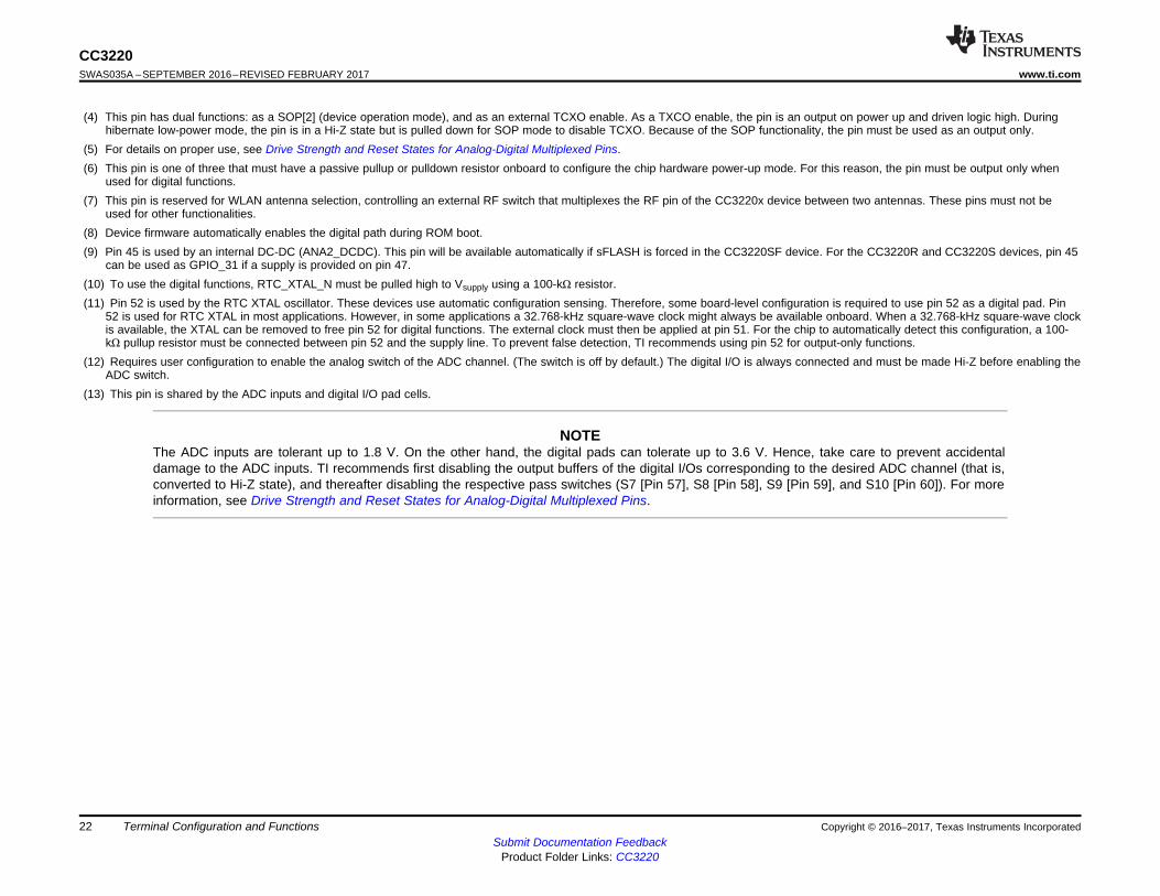
(4) This pin has dual functions: as a SOP[2] (device operation mode), and as an external TCXO enable. As a TXCO enable, the pin is an output on power up and driven logic high. Duringhibernate low-power mode, the pin is in a Hi-Z state but is pulled down for SOP mode to disable TCXO. Because of the SOP functionality, the pin must be used as an output only.
(5) For details on proper use, see Drive Strength and Reset States for Analog-Digital Multiplexed Pins.(6) This pin is one of three that must have a passive pullup or pulldown resistor onboard to configure the chip hardware power-up mode. For this reason, the pin must be output only when
used for digital functions.(7) This pin is reserved for WLAN antenna selection, controlling an external RF switch that multiplexes the RF pin of the CC3220x device between two antennas. These pins must not be
used for other functionalities.(8) Device firmware automatically enables the digital path during ROM boot.(9) Pin 45 is used by an internal DC-DC (ANA2_DCDC). This pin will be available automatically if sFLASH is forced in the CC3220SF device. For the CC3220R and CC3220S devices, pin 45
can be used as GPIO_31 if a supply is provided on pin 47.(10) To use the digital functions, RTC_XTAL_N must be pulled high to Vsupply using a 100-kΩ resistor.(11) Pin 52 is used by the RTC XTAL oscillator. These devices use automatic configuration sensing. Therefore, some board-level configuration is required to use pin 52 as a digital pad. Pin
52 is used for RTC XTAL in most applications. However, in some applications a 32.768-kHz square-wave clock might always be available onboard. When a 32.768-kHz square-wave clockis available, the XTAL can be removed to free pin 52 for digital functions. The external clock must then be applied at pin 51. For the chip to automatically detect this configuration, a 100-kΩ pullup resistor must be connected between pin 52 and the supply line. To prevent false detection, TI recommends using pin 52 for output-only functions.
(12) Requires user configuration to enable the analog switch of the ADC channel. (The switch is off by default.) The digital I/O is always connected and must be made Hi-Z before enabling theADC switch.
(13) This pin is shared by the ADC inputs and digital I/O pad cells.
NOTEThe ADC inputs are tolerant up to 1.8 V. On the other hand, the digital pads can tolerate up to 3.6 V. Hence, take care to prevent accidentaldamage to the ADC inputs. TI recommends first disabling the output buffers of the digital I/Os corresponding to the desired ADC channel (that is,converted to Hi-Z state), and thereafter disabling the respective pass switches (S7 [Pin 57], S8 [Pin 58], S9 [Pin 59], and S10 [Pin 60]). For moreinformation, see Drive Strength and Reset States for Analog-Digital Multiplexed Pins.
23
CC3220www.ti.com SWAS035A –SEPTEMBER 2016–REVISED FEBRUARY 2017
Submit Documentation FeedbackProduct Folder Links: CC3220
Terminal Configuration and FunctionsCopyright © 2016–2017, Texas Instruments Incorporated
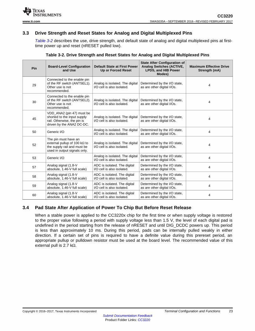
3.3 Drive Strength and Reset States for Analog and Digital Multiplexed PinsTable 3-2 describes the use, drive strength, and default state of analog and digital multiplexed pins at first-time power up and reset (nRESET pulled low).
Table 3-2. Drive Strength and Reset States for Analog and Digital Multiplexed Pins
Pin Board-Level Configurationand Use
Default State at First PowerUp or Forced Reset
State After Configuration ofAnalog Switches (ACTIVE,
LPDS, and HIB PowerModes)
Maximum Effective DriveStrength (mA)
29
Connected to the enable pinof the RF switch (ANTSEL1).Other use is notrecommended.
Analog is isolated. The digitalI/O cell is also isolated.
Determined by the I/O state,as are other digital I/Os. 4
30
Connected to the enable pinof the RF switch (ANTSEL2).Other use is notrecommended.
Analog is isolated. The digitalI/O cell is also isolated.
Determined by the I/O state,as are other digital I/Os. 4
45
VDD_ANA2 (pin 47) must beshorted to the input supplyrail. Otherwise, the pin isdriven by the ANA2 DC-DC.
Analog is isolated. The digitalI/O cell is also isolated.
Determined by the I/O state,as are other digital I/Os. 4
50 Generic I/O Analog is isolated. The digitalI/O cell is also isolated.
Determined by the I/O state,as are other digital I/Os. 4
52
The pin must have anexternal pullup of 100 kΩ tothe supply rail and must beused in output signals only.
Analog is isolated. The digitalI/O cell is also isolated.
Determined by the I/O state,as are other digital I/Os. 4
53 Generic I/O Analog is isolated. The digitalI/O cell is also isolated.
Determined by the I/O state,as are other digital I/Os. 4
57 Analog signal (1.8-Vabsolute, 1.46-V full scale)
ADC is isolated. The digitalI/O cell is also isolated.
Determined by the I/O state,as are other digital I/Os. 4
58 Analog signal (1.8-Vabsolute, 1.46-V full scale)
ADC is isolated. The digitalI/O cell is also isolated.
Determined by the I/O state,as are other digital I/Os. 4
59 Analog signal (1.8-Vabsolute, 1.46-V full scale)
ADC is isolated. The digitalI/O cell is also isolated.
Determined by the I/O state,as are other digital I/Os. 4
60 Analog signal (1.8-Vabsolute, 1.46-V full scale)
ADC is isolated. The digitalI/O cell is also isolated.
Determined by the I/O state,as are other digital I/Os. 4
3.4 Pad State After Application of Power To Chip But Before Reset ReleaseWhen a stable power is applied to the CC3220x chip for the first time or when supply voltage is restoredto the proper value following a period with supply voltage less than 1.5 V, the level of each digital pad isundefined in the period starting from the release of nRESET and until DIG_DCDC powers up. This periodis less than approximately 10 ms. During this period, pads can be internally pulled weakly in eitherdirection. If a certain set of pins is required to have a definite value during this prereset period, anappropriate pullup or pulldown resistor must be used at the board level. The recommended value of thisexternal pull is 2.7 kΩ.
24
CC3220SWAS035A –SEPTEMBER 2016–REVISED FEBRUARY 2017 www.ti.com
Submit Documentation FeedbackProduct Folder Links: CC3220
Terminal Configuration and Functions Copyright © 2016–2017, Texas Instruments Incorporated
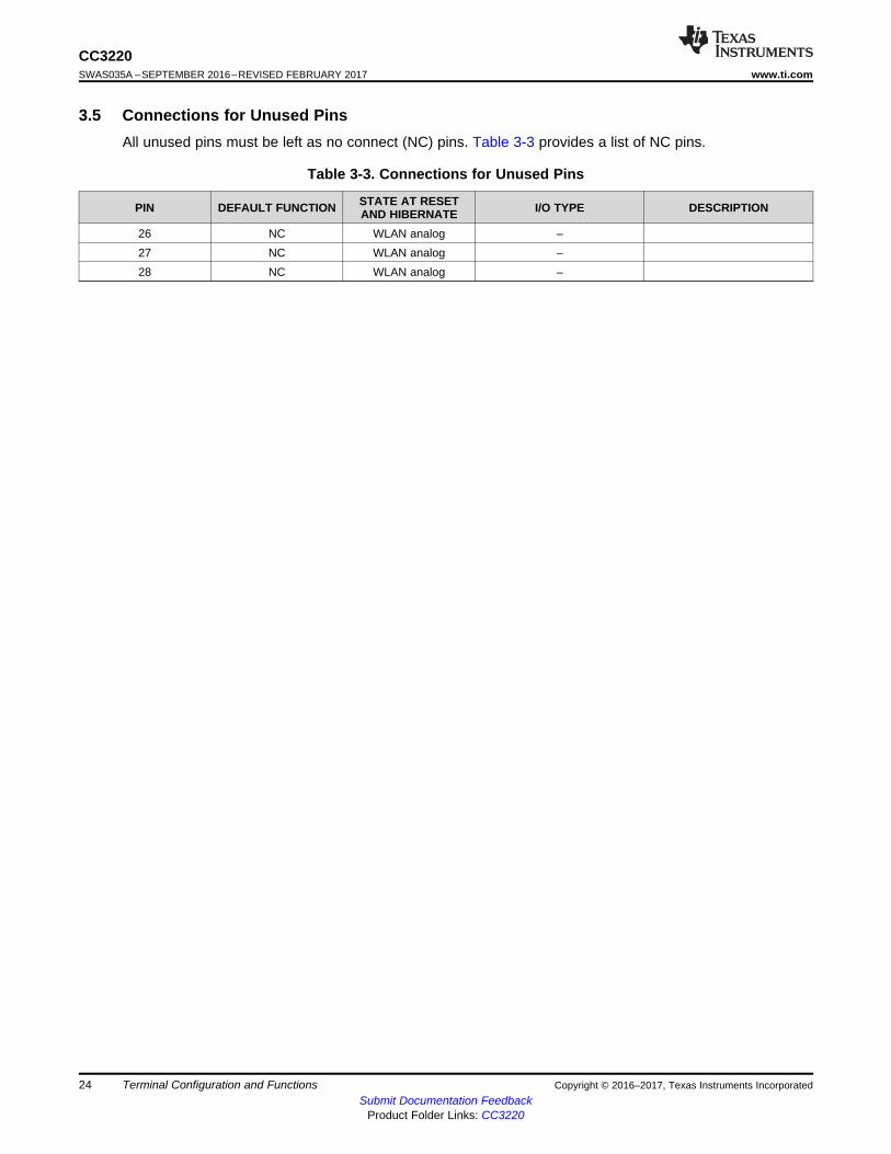
3.5 Connections for Unused PinsAll unused pins must be left as no connect (NC) pins. Table 3-3 provides a list of NC pins.
Table 3-3. Connections for Unused Pins
PIN DEFAULT FUNCTION STATE AT RESETAND HIBERNATE I/O TYPE DESCRIPTION
26 NC WLAN analog –27 NC WLAN analog –28 NC WLAN analog –
25
CC3220www.ti.com SWAS035A –SEPTEMBER 2016–REVISED FEBRUARY 2017
Submit Documentation FeedbackProduct Folder Links: CC3220
SpecificationsCopyright © 2016–2017, Texas Instruments Incorporated
4 Specifications
All measurements are referenced at the device pins, unless otherwise indicated. All specifications are overprocess and voltage, unless otherwise indicated.
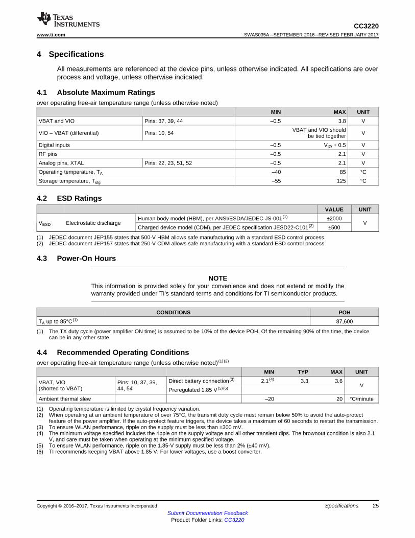
4.1 Absolute Maximum Ratingsover operating free-air temperature range (unless otherwise noted)
MIN MAX UNITVBAT and VIO Pins: 37, 39, 44 –0.5 3.8 V
VIO – VBAT (differential) Pins: 10, 54 VBAT and VIO shouldbe tied together V
Digital inputs –0.5 VIO + 0.5 VRF pins –0.5 2.1 VAnalog pins, XTAL Pins: 22, 23, 51, 52 –0.5 2.1 VOperating temperature, TA –40 85 °CStorage temperature, Tstg –55 125 °C
(1) JEDEC document JEP155 states that 500-V HBM allows safe manufacturing with a standard ESD control process.(2) JEDEC document JEP157 states that 250-V CDM allows safe manufacturing with a standard ESD control process.
4.2 ESD RatingsVALUE UNIT
VESD Electrostatic dischargeHuman body model (HBM), per ANSI/ESDA/JEDEC JS-001 (1) ±2000
VCharged device model (CDM), per JEDEC specification JESD22-C101 (2) ±500
4.3 Power-On Hours
NOTEThis information is provided solely for your convenience and does not extend or modify thewarranty provided under TI's standard terms and conditions for TI semiconductor products.
(1) The TX duty cycle (power amplifier ON time) is assumed to be 10% of the device POH. Of the remaining 90% of the time, the devicecan be in any other state.
CONDITIONS POHTA up to 85°C (1) 87,600
(1) Operating temperature is limited by crystal frequency variation.(2) When operating at an ambient temperature of over 75°C, the transmit duty cycle must remain below 50% to avoid the auto-protect
feature of the power amplifier. If the auto-protect feature triggers, the device takes a maximum of 60 seconds to restart the transmission.(3) To ensure WLAN performance, ripple on the supply must be less than ±300 mV.(4) The minimum voltage specified includes the ripple on the supply voltage and all other transient dips. The brownout condition is also 2.1
V, and care must be taken when operating at the minimum specified voltage.(5) To ensure WLAN performance, ripple on the 1.85-V supply must be less than 2% (±40 mV).(6) TI recommends keeping VBAT above 1.85 V. For lower voltages, use a boost converter.
4.4 Recommended Operating Conditionsover operating free-air temperature range (unless otherwise noted) (1) (2)
MIN TYP MAX UNIT
VBAT, VIO(shorted to VBAT)
Pins: 10, 37, 39,44, 54
Direct battery connection (3) 2.1 (4) 3.3 3.6V
Preregulated 1.85 V (5) (6)
Ambient thermal slew –20 20 °C/minute
26
CC3220SWAS035A –SEPTEMBER 2016–REVISED FEBRUARY 2017 www.ti.com
Submit Documentation FeedbackProduct Folder Links: CC3220
Specifications Copyright © 2016–2017, Texas Instruments Incorporated
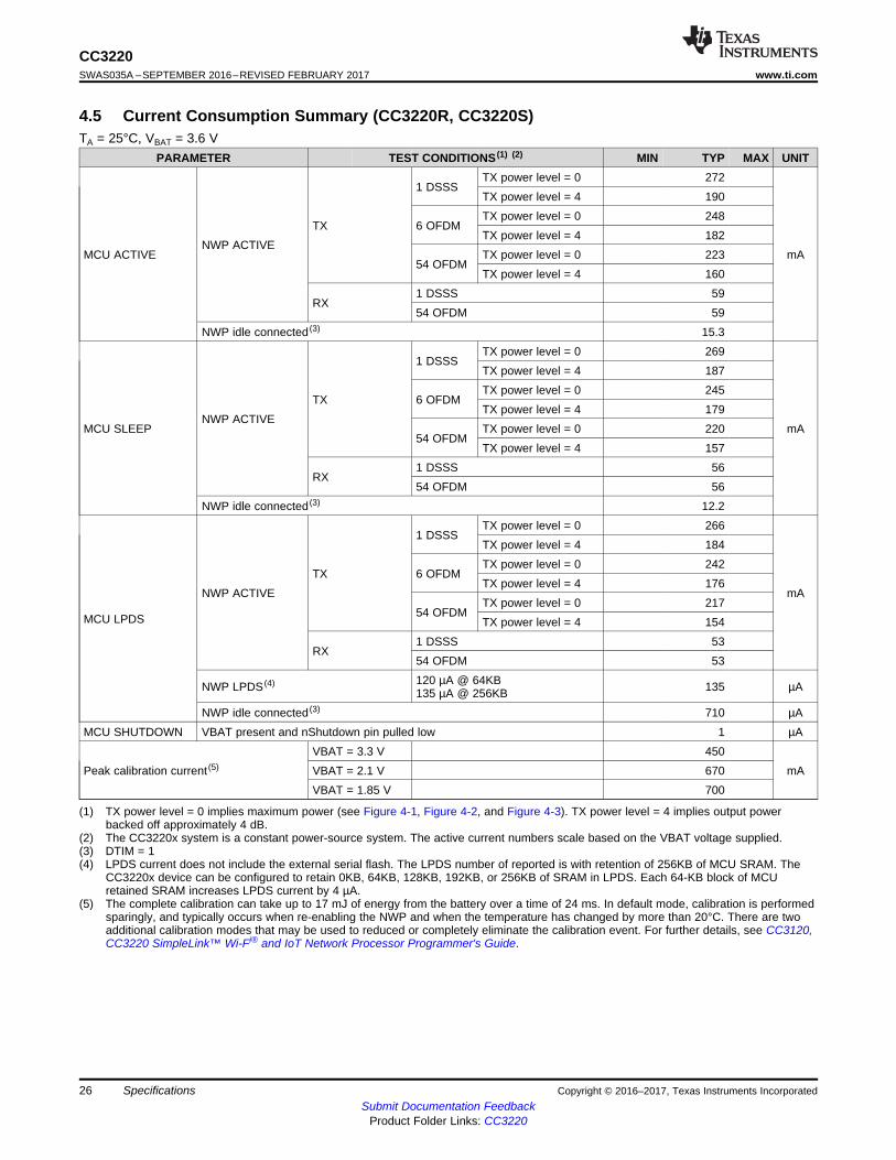
(1) TX power level = 0 implies maximum power (see Figure 4-1, Figure 4-2, and Figure 4-3). TX power level = 4 implies output powerbacked off approximately 4 dB.
(2) The CC3220x system is a constant power-source system. The active current numbers scale based on the VBAT voltage supplied.(3) DTIM = 1(4) LPDS current does not include the external serial flash. The LPDS number of reported is with retention of 256KB of MCU SRAM. The
CC3220x device can be configured to retain 0KB, 64KB, 128KB, 192KB, or 256KB of SRAM in LPDS. Each 64-KB block of MCUretained SRAM increases LPDS current by 4 µA.
(5) The complete calibration can take up to 17 mJ of energy from the battery over a time of 24 ms. In default mode, calibration is performedsparingly, and typically occurs when re-enabling the NWP and when the temperature has changed by more than 20°C. There are twoadditional calibration modes that may be used to reduced or completely eliminate the calibration event. For further details, see CC3120,CC3220 SimpleLink™ Wi-Fi® and IoT Network Processor Programmer's Guide.
4.5 Current Consumption Summary (CC3220R, CC3220S)TA = 25°C, VBAT = 3.6 V
PARAMETER TEST CONDITIONS (1) (2) MIN TYP MAX UNIT
MCU ACTIVENWP ACTIVE
TX
1 DSSSTX power level = 0 272
mA
TX power level = 4 190
6 OFDMTX power level = 0 248TX power level = 4 182
54 OFDMTX power level = 0 223TX power level = 4 160
RX1 DSSS 5954 OFDM 59
NWP idle connected (3) 15.3
MCU SLEEPNWP ACTIVE
TX
1 DSSSTX power level = 0 269
mA
TX power level = 4 187
6 OFDMTX power level = 0 245TX power level = 4 179
54 OFDMTX power level = 0 220TX power level = 4 157
RX1 DSSS 5654 OFDM 56
NWP idle connected (3) 12.2
MCU LPDS
NWP ACTIVETX
1 DSSSTX power level = 0 266
mA
TX power level = 4 184
6 OFDMTX power level = 0 242TX power level = 4 176
54 OFDMTX power level = 0 217TX power level = 4 154
RX1 DSSS 5354 OFDM 53
NWP LPDS (4) 120 µA @ 64KB135 µA @ 256KB 135 µA
NWP idle connected (3) 710 µAMCU SHUTDOWN VBAT present and nShutdown pin pulled low 1 µA
Peak calibration current (5)
VBAT = 3.3 V 450mAVBAT = 2.1 V 670
VBAT = 1.85 V 700
27
CC3220www.ti.com SWAS035A –SEPTEMBER 2016–REVISED FEBRUARY 2017
Submit Documentation FeedbackProduct Folder Links: CC3220
SpecificationsCopyright © 2016–2017, Texas Instruments Incorporated
(1) TX power level = 0 implies maximum power (see Figure 4-1, Figure 4-2, and Figure 4-3). TX power level = 4 implies output powerbacked off approximately 4 dB.
(2) The CC3220x system is a constant power-source system. The active current numbers scale based on the VBAT voltage supplied.(3) DTIM = 1(4) LPDS current does not include the external serial flash. The LPDS number of reported is with retention of 256KB of MCU SRAM. The
CC3220x device can be configured to retain 0KB, 64KB, 128KB, 192KB, or 256KB of SRAM in LPDS. Each 64-KB block of MCUretained SRAM increases LPDS current by 4 µA.
(5) The complete calibration can take up to 17 mJ of energy from the battery over a period of 24 ms. Calibration is performed sparingly,typically when coming out of HIBERNATE and only if temperature has changed by more than 20°C. The calibration event can becontrolled by a configuration file in the serial flash..
4.6 Current Consumption Summary (CC3200SF)TA = 25°C, VBAT = 3.6 V
PARAMETER TEST CONDITIONS (1) (2) MIN TYP MAX UNIT
MCU ACTIVENWP ACTIVE
TX
1 DSSSTX power level = maximum 286
mA
TX power level = maximum – 4 202
6 OFDMTX power level = maximum 255TX power level = maximum – 4 192
54 OFDMTX power level = maximum 232TX power level = maximum – 4 174
RX1 DSSS 7454 OFDM 74
NWP idle connected (3) 25.2
MCU SLEEPNWP ACTIVE
TX
1 DSSSTX power level = maximum 282
mA
TX power level = maximum – 4 198
6 OFDMTX power level = maximum 251TX power level = maximum – 4 188
54 OFDMTX power level = maximum 228TX power level = maximum – 4 170
RX1 DSSS 7054 OFDM 70
NWP idle connected (3) 21.2
MCU LPDS
NWP activeTX
1 DSSSTX power level = 0 266
mA
TX power level = 4 184
6 OFDMTX power level = 0 242TX power level = 4 176
54 OFDMTX power level = 0 217TX power level = 4 154
RX1 DSSS 5354 OFDM 53
NWP LPDS (4) 120 µA @ 64KB135 µA @ 256KB 135 µA
NWP idle connected (3) 710 µAMCUSHUTDOWN VBAT present and nReset pin pulled low 1 µA
Peak calibration current (5)
VBAT = 3.3 V 450mAVBAT = 2.1 V 670
VBAT = 1.85 V 700
TX power level setting
TX
Pow
er
(dB
m)
19.00
17.00
15.00
13.00
11.00
9.00
7.00
5.00
3.00
1.00
0 1 2 3 4 5 6 7 8 9 10 11 12 13 14 15
IBA
T(V
BA
T@
3.6
V)(
mA
mp)
280.00
264.40
249.00
233.30
218.00
202.00
186.70
171.00
155.60
140.00
6 OFDM
Color by
TX Power (dBm)
IBAT (VBAT @ 3.6 V)
TX power level setting
TX
Pow
er
(dB
m)
19.00
17.00
15.00
13.00
11.00
9.00
7.00
5.00
3.00
1.00
0 1 2 3 4 5 6 7 8 9 10 11 12 13 14 15
280.00
264.40
249.00
233.30
218.00
202.00
186.70
171.00
155.60
140.00
1 DSSS
IBA
T(V
BA
T@
3.6
V)(
mA
mp)
Color by
TX Power (dBm)
IBAT (VBAT @ 3.6 V)
28
CC3220SWAS035A –SEPTEMBER 2016–REVISED FEBRUARY 2017 www.ti.com
Submit Documentation FeedbackProduct Folder Links: CC3220
Specifications Copyright © 2016–2017, Texas Instruments Incorporated
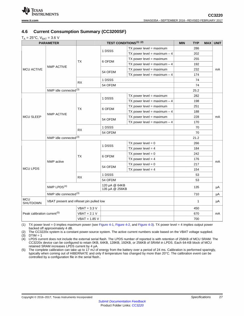
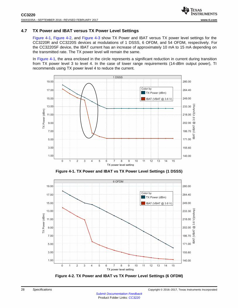
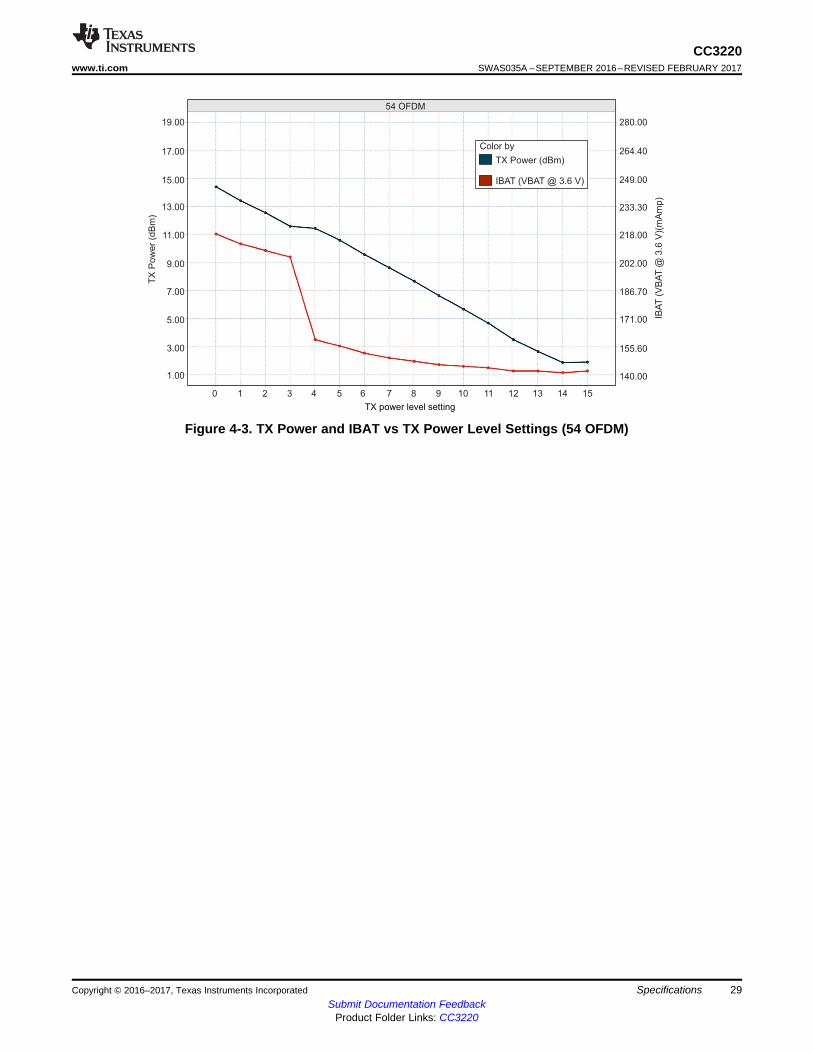
4.7 TX Power and IBAT versus TX Power Level SettingsFigure 4-1, Figure 4-2, and Figure 4-3 show TX Power and IBAT versus TX power level settings for theCC3220R and CC3220S devices at modulations of 1 DSSS, 6 OFDM, and 54 OFDM, respectively. Forthe CC3220SF device, the IBAT current has an increase of approximately 10 mA to 15 mA depending onthe transmitted rate. The TX power level will remain the same.
In Figure 4-1, the area enclosed in the circle represents a significant reduction in current during transitionfrom TX power level 3 to level 4. In the case of lower range requirements (14-dBm output power), TIrecommends using TX power level 4 to reduce the current.
Figure 4-1. TX Power and IBAT vs TX Power Level Settings (1 DSSS)
Figure 4-2. TX Power and IBAT vs TX Power Level Settings (6 OFDM)
TX power level setting
TX
Pow
er
(dB
m)
19.00
17.00
15.00
13.00
11.00
9.00
7.00
5.00
3.00
1.00
0 1 2 3 4 5 6 7 8 9 10 11 12 13 14 15
54 OFDM
280.00
264.40
249.00
233.30
218.00
202.00
186.70
171.00
155.60
140.00
IBA
T(V
BA
T@
3.6
V)(
mA
mp)
Color by
TX Power (dBm)
IBAT (VBAT @ 3.6 V)
29
CC3220www.ti.com SWAS035A –SEPTEMBER 2016–REVISED FEBRUARY 2017
Submit Documentation FeedbackProduct Folder Links: CC3220
SpecificationsCopyright © 2016–2017, Texas Instruments Incorporated
Figure 4-3. TX Power and IBAT vs TX Power Level Settings (54 OFDM)
30
CC3220SWAS035A –SEPTEMBER 2016–REVISED FEBRUARY 2017 www.ti.com
Submit Documentation FeedbackProduct Folder Links: CC3220
Specifications Copyright © 2016–2017, Texas Instruments Incorporated
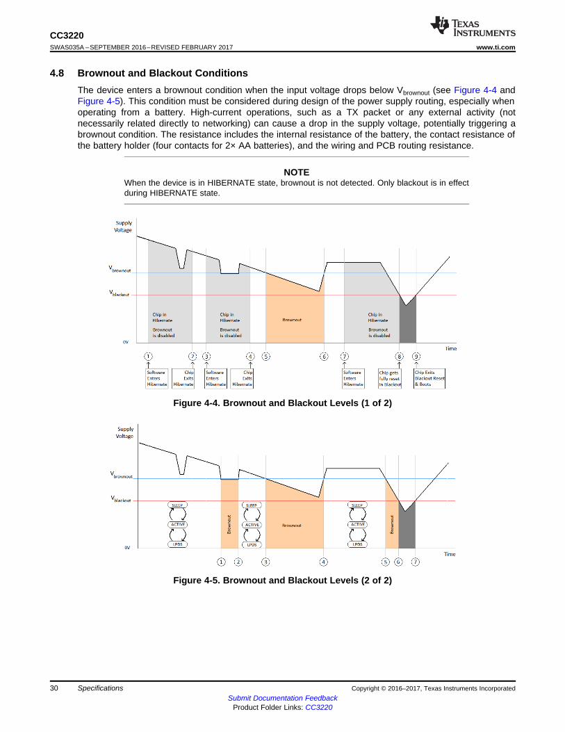
4.8 Brownout and Blackout ConditionsThe device enters a brownout condition when the input voltage drops below Vbrownout (see Figure 4-4 andFigure 4-5). This condition must be considered during design of the power supply routing, especially whenoperating from a battery. High-current operations, such as a TX packet or any external activity (notnecessarily related directly to networking) can cause a drop in the supply voltage, potentially triggering abrownout condition. The resistance includes the internal resistance of the battery, the contact resistance ofthe battery holder (four contacts for 2× AA batteries), and the wiring and PCB routing resistance.
NOTEWhen the device is in HIBERNATE state, brownout is not detected. Only blackout is in effectduring HIBERNATE state.
Figure 4-4. Brownout and Blackout Levels (1 of 2)
Figure 4-5. Brownout and Blackout Levels (2 of 2)
31
CC3220www.ti.com SWAS035A –SEPTEMBER 2016–REVISED FEBRUARY 2017
Submit Documentation FeedbackProduct Folder Links: CC3220
SpecificationsCopyright © 2016–2017, Texas Instruments Incorporated
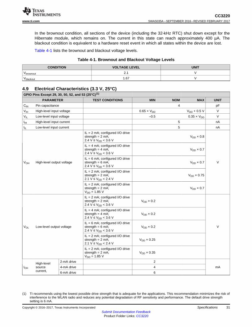
In the brownout condition, all sections of the device (including the 32-kHz RTC) shut down except for theHibernate module, which remains on. The current in this state can reach approximately 400 µA. Theblackout condition is equivalent to a hardware reset event in which all states within the device are lost.
Table 4-1 lists the brownout and blackout voltage levels.
Table 4-1. Brownout and Blackout Voltage Levels
CONDITION VOLTAGE LEVEL UNITVbrownout 2.1 VVblackout 1.67 V
4.9 Electrical Characteristics (3.3 V, 25°C)
(1) TI recommends using the lowest possible drive strength that is adequate for the applications. This recommendation minimizes the risk ofinterference to the WLAN radio and reduces any potential degradation of RF sensitivity and performance. The default drive strengthsetting is 6 mA.
GPIO Pins Except 29, 30, 50, 52, and 53 (25°C) (1)
PARAMETER TEST CONDITIONS MIN NOM MAX UNITCIN Pin capacitance 4 pFVIH High-level input voltage 0.65 × VDD VDD + 0.5 V VVIL Low-level input voltage –0.5 0.35 × VDD VIIH High-level input current 5 nAIIL Low-level input current 5 nA
VOH High-level output voltage
IL = 2 mA; configured I/O drivestrength = 2 mA;2.4 V ≤ VDD < 3.6 V
VDD × 0.8
V
IL = 4 mA; configured I/O drivestrength = 4 mA;2.4 V ≤ VDD < 3.6 V
VDD × 0.7
IL = 6 mA; configured I/O drivestrength = 6 mA;2.4 V ≤ VDD < 3.6 V
VDD × 0.7
IL = 2 mA; configured I/O drivestrength = 2 mA;2.1 V ≤ VDD < 2.4 V
VDD × 0.75
IL = 2 mA; configured I/O drivestrength = 2 mA;VDD = 1.85 V
VDD × 0.7
VOL Low-level output voltage
IL = 2 mA; configured I/O drivestrength = 2 mA;2.4 V ≤ VDD < 3.6 V
VDD × 0.2
V
IL = 4 mA; configured I/O drivestrength = 4 mA;2.4 V ≤ VDD < 3.6 V
VDD × 0.2
IL = 6 mA; configured I/O drivestrength = 6 mA;2.4 V ≤ VDD < 3.6 V
VDD × 0.2
IL = 2 mA; configured I/O drivestrength = 2 mA;2.1 V ≤ VDD < 2.4 V
VDD × 0.25
IL = 2 mA; configured I/O drivestrength = 2 mA;VDD = 1.85 V
VDD × 0.35
IOH
High-levelsourcecurrent,
2-mA drive 2mA4-mA drive 4
6-mA drive 6
32
CC3220SWAS035A –SEPTEMBER 2016–REVISED FEBRUARY 2017 www.ti.com
Submit Documentation FeedbackProduct Folder Links: CC3220
Specifications Copyright © 2016–2017, Texas Instruments Incorporated
GPIO Pins Except 29, 30, 50, 52, and 53 (25°C) (1)
PARAMETER TEST CONDITIONS MIN NOM MAX UNIT
IOLLow-level sinkcurrent,
2-mA drive 2mA4-mA drive 4
6-mA drive 6
(1) TI recommends using the lowest possible drive strength that is adequate for the applications. This recommendation minimizes the risk ofinterference to the WLAN radio and reduces any potential degradation of RF sensitivity and performance. The default drive strengthsetting is 6 mA.
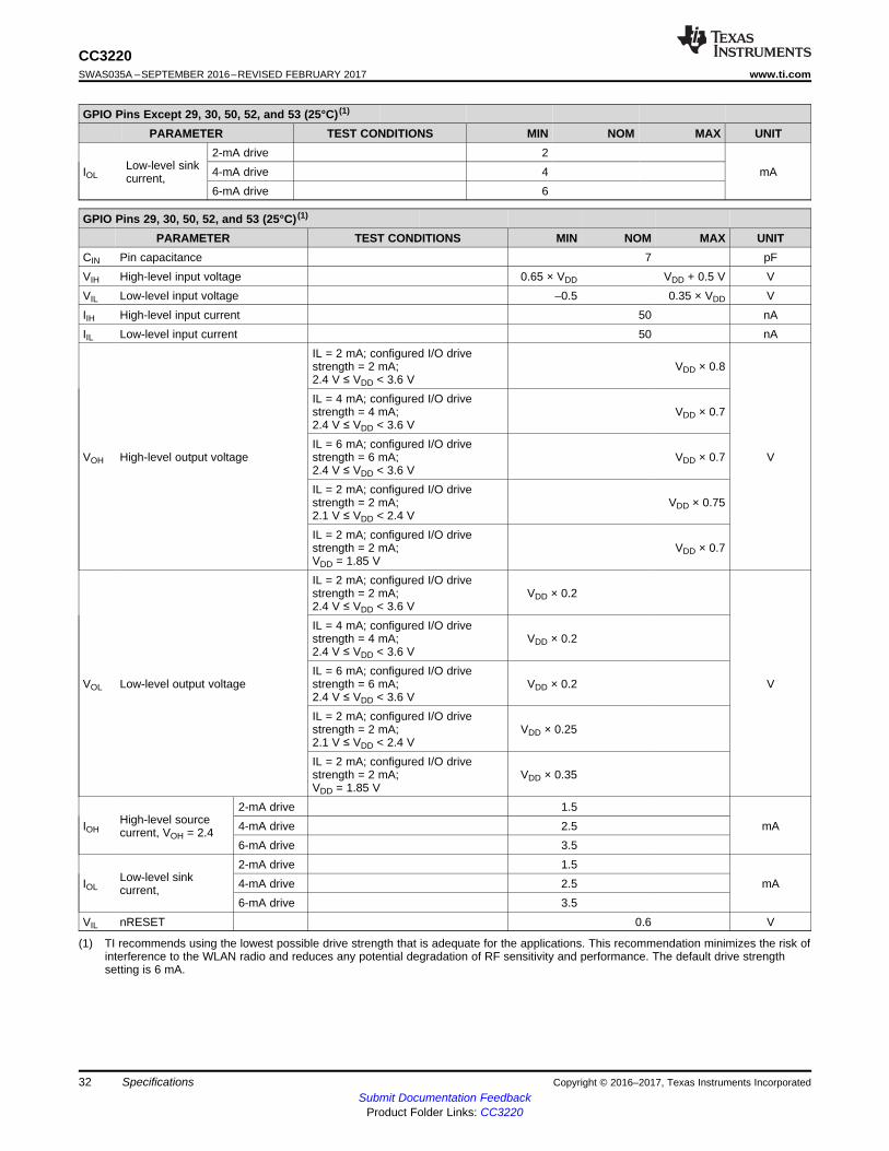
GPIO Pins 29, 30, 50, 52, and 53 (25°C) (1)
PARAMETER TEST CONDITIONS MIN NOM MAX UNITCIN Pin capacitance 7 pFVIH High-level input voltage 0.65 × VDD VDD + 0.5 V VVIL Low-level input voltage –0.5 0.35 × VDD VIIH High-level input current 50 nAIIL Low-level input current 50 nA
VOH High-level output voltage
IL = 2 mA; configured I/O drivestrength = 2 mA;2.4 V ≤ VDD < 3.6 V
VDD × 0.8
V
IL = 4 mA; configured I/O drivestrength = 4 mA;2.4 V ≤ VDD < 3.6 V
VDD × 0.7
IL = 6 mA; configured I/O drivestrength = 6 mA;2.4 V ≤ VDD < 3.6 V
VDD × 0.7
IL = 2 mA; configured I/O drivestrength = 2 mA;2.1 V ≤ VDD < 2.4 V
VDD × 0.75
IL = 2 mA; configured I/O drivestrength = 2 mA;VDD = 1.85 V
VDD × 0.7
VOL Low-level output voltage
IL = 2 mA; configured I/O drivestrength = 2 mA;2.4 V ≤ VDD < 3.6 V
VDD × 0.2
V
IL = 4 mA; configured I/O drivestrength = 4 mA;2.4 V ≤ VDD < 3.6 V
VDD × 0.2
IL = 6 mA; configured I/O drivestrength = 6 mA;2.4 V ≤ VDD < 3.6 V
VDD × 0.2
IL = 2 mA; configured I/O drivestrength = 2 mA;2.1 V ≤ VDD < 2.4 V
VDD × 0.25
IL = 2 mA; configured I/O drivestrength = 2 mA;VDD = 1.85 V
VDD × 0.35
IOHHigh-level sourcecurrent, VOH = 2.4
2-mA drive 1.5mA4-mA drive 2.5
6-mA drive 3.5
IOLLow-level sinkcurrent,
2-mA drive 1.5mA4-mA drive 2.5
6-mA drive 3.5VIL nRESET 0.6 V
33
CC3220www.ti.com SWAS035A –SEPTEMBER 2016–REVISED FEBRUARY 2017
Submit Documentation FeedbackProduct Folder Links: CC3220
SpecificationsCopyright © 2016–2017, Texas Instruments Incorporated
Pin Internal Pullup and Pulldown (25°C)PARAMETER TEST CONDITIONS MIN NOM MAX UNIT
IOHPullup current, VOH = 2.4(VDD = 3.0 V) 5 10 µA
IOLPulldown current, VOL = 0.4(VDD = 3.0 V) 5 µA
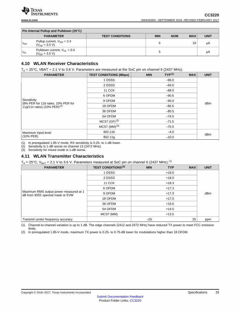
4.10 WLAN Receiver Characteristics
(1) In preregulated 1.85-V mode, RX sensitivity is 0.25- to 1-dB lower.(2) Sensitivity is 1-dB worse on channel 13 (2472 MHz).(3) Sensitivity for mixed mode is 1-dB worse.
TA = 25°C, VBAT = 2.1 V to 3.6 V. Parameters are measured at the SoC pin on channel 6 (2437 MHz).PARAMETER TEST CONDITIONS (Mbps) MIN TYP (1) MAX UNIT
Sensitivity(8% PER for 11b rates, 10% PER for11g/11n rates) (10% PER) (2)
1 DSSS –96.0
dBm
2 DSSS –94.011 CCK –88.06 OFDM –90.59 OFDM –90.0
18 OFDM –86.536 OFDM –80.554 OFDM –74.5
MCS7 (GF) (3) –71.5MCS7 (MM) (3) –70.5
Maximum input level(10% PER)
802.11b –4.0dBm
802.11g –10.0
4.11 WLAN Transmitter Characteristics
(1) Channel-to-channel variation is up to 1 dB. The edge channels (2412 and 2472 MHz) have reduced TX power to meet FCC emissionlimits.
(2) In preregulated 1.85-V mode, maximum TX power is 0.25- to 0.75-dB lower for modulations higher than 18 OFDM.
TA = 25°C, VBAT = 2.1 V to 3.6 V. Parameters measured at SoC pin on channel 6 (2437 MHz). (1)
PARAMETER TEST CONDITIONS (2) MIN TYP MAX UNIT
Maximum RMS output power measured at 1dB from IEEE spectral mask or EVM
1 DSSS +18.0
dBm
2 DSSS +18.011 CCK +18.36 OFDM +17.39 OFDM +17.3
18 OFDM +17.036 OFDM +16.054 OFDM +14.5
MCS7 (MM) +13.0Transmit center frequency accuracy –25 25 ppm
34
CC3220SWAS035A –SEPTEMBER 2016–REVISED FEBRUARY 2017 www.ti.com
Submit Documentation FeedbackProduct Folder Links: CC3220
Specifications Copyright © 2016–2017, Texas Instruments Incorporated
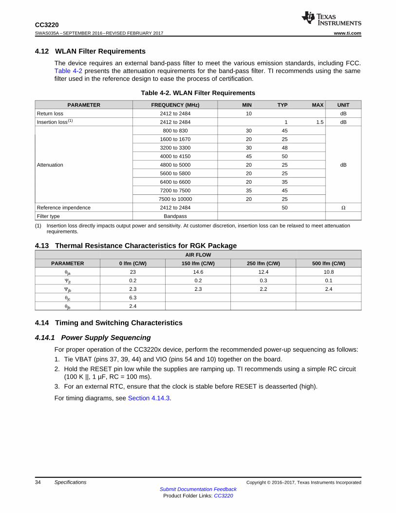
(1) Insertion loss directly impacts output power and sensitivity. At customer discretion, insertion loss can be relaxed to meet attenuationrequirements.
4.12 WLAN Filter RequirementsThe device requires an external band-pass filter to meet the various emission standards, including FCC.Table 4-2 presents the attenuation requirements for the band-pass filter. TI recommends using the samefilter used in the reference design to ease the process of certification.
Table 4-2. WLAN Filter Requirements
PARAMETER FREQUENCY (MHz) MIN TYP MAX UNITReturn loss 2412 to 2484 10 dBInsertion loss (1) 2412 to 2484 1 1.5 dB
Attenuation
800 to 830 30 45
dB
1600 to 1670 20 253200 to 3300 30 484000 to 4150 45 504800 to 5000 20 255600 to 5800 20 256400 to 6600 20 357200 to 7500 35 457500 to 10000 20 25
Reference impendence 2412 to 2484 50 Ω
Filter type Bandpass
4.13 Thermal Resistance Characteristics for RGK PackageAIR FLOW
PARAMETER 0 lfm (C/W) 150 lfm (C/W) 250 lfm (C/W) 500 lfm (C/W)θja 23 14.6 12.4 10.8Ψjt 0.2 0.2 0.3 0.1Ψjb 2.3 2.3 2.2 2.4θjc 6.3θjb 2.4
4.14 Timing and Switching Characteristics
4.14.1 Power Supply SequencingFor proper operation of the CC3220x device, perform the recommended power-up sequencing as follows:1. Tie VBAT (pins 37, 39, 44) and VIO (pins 54 and 10) together on the board.2. Hold the RESET pin low while the supplies are ramping up. TI recommends using a simple RC circuit
(100 K ||, 1 µF, RC = 100 ms).3. For an external RTC, ensure that the clock is stable before RESET is deasserted (high).
For timing diagrams, see Section 4.14.3.
POWER
OFFHW INIT FW INIT
APP CODE
EXECUTION
VBAT
VIO
nRESET
STATE
T1 T2 T3
RESET
T4
32-kHz
RTC CLK
APP CODE
LOAD
35
CC3220www.ti.com SWAS035A –SEPTEMBER 2016–REVISED FEBRUARY 2017
Submit Documentation FeedbackProduct Folder Links: CC3220
SpecificationsCopyright © 2016–2017, Texas Instruments Incorporated
4.14.2 Device ResetWhen a device restart is required, the user may issue a negative pulse to the nRESET pin. The user mustfollow one of the two alternatives to ensure the reset is properly applied:• A negative reset pulse (on pin 32) of at least 200-mS duration• If the above cannot be guaranteed, a pull-down resistor of 2M Ω should be connected to pin 32
(RTC_XTAL_N). if implemented, a shorter pulse of at least 100 µs can be used.
To ensure a proper reset sequence, the user has to call the sl_stop function prior to toggling the reset. It ispreferable to use software reset instead of an external trigger when a reset is required.
4.14.3 Reset Timing
4.14.3.1 nRESET (32k XTAL)
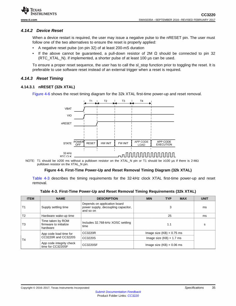
Figure 4-6 shows the reset timing diagram for the 32k XTAL first-time power-up and reset removal.
NOTE: T1 should be ≥200 ms without a pulldown resistor on the XTAL_N pin or T1 should be ≥100 µs if there is 2-MΩpulldown resistor on the XTAL_N pin.
Figure 4-6. First-Time Power-Up and Reset Removal Timing Diagram (32k XTAL)
Table 4-3 describes the timing requirements for the 32-kHz clock XTAL first-time power-up and resetremoval.
Table 4-3. First-Time Power-Up and Reset Removal Timing Requirements (32k XTAL)
ITEM NAME DESCRIPTION MIN TYP MAX UNIT
T1 Supply settling timeDepends on application boardpower supply, decoupling capacitor,and so on
3 ms
T2 Hardware wake-up time 25 ms
T3Time taken by ROMfirmware to initializehardware
Includes 32.768-kHz XOSC settlingtime 1.1 s
T4
App code load time forCC3220R and CC3220S
CC3220R Image size (KB) × 0.75 msCC3220S Image size (KB) × 1.7 ms
App code integrity checktime for CC3220SF CC3220SF Image size (KB) × 0.06 ms
POWER
OFFHW INIT FW INIT
APP CODE
EXECUTION
VBAT
VIO
nRESET
STATE
T1 T2 T3
RESET
T4
32-kHz
RTC CLK
APP CODE
LOAD
36
CC3220SWAS035A –SEPTEMBER 2016–REVISED FEBRUARY 2017 www.ti.com
Submit Documentation FeedbackProduct Folder Links: CC3220
Specifications Copyright © 2016–2017, Texas Instruments Incorporated
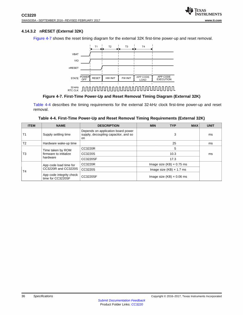
4.14.3.2 nRESET (External 32K)
Figure 4-7 shows the reset timing diagram for the external 32K first-time power-up and reset removal.
Figure 4-7. First-Time Power-Up and Reset Removal Timing Diagram (External 32K)
Table 4-4 describes the timing requirements for the external 32-kHz clock first-time power-up and resetremoval.
Table 4-4. First-Time Power-Up and Reset Removal Timing Requirements (External 32K)
ITEM NAME DESCRIPTION MIN TYP MAX UNIT
T1 Supply settling timeDepends on application board powersupply, decoupling capacitor, and soon
3 ms
T2 Hardware wake-up time 25 ms
T3Time taken by ROMfirmware to initializehardware
CC3220R 5msCC3220S 10.3
CC3220SF 17.3
T4
App code load time forCC3220R and CC3220S
CC3220R Image size (KB) × 0.75 msCC3220S Image size (KB) × 1.7 ms
App code integrity checktime for CC3220SF CC3220SF Image size (KB) × 0.06 ms
ACTIVE HIBERNATE HW WAKEUP FW INITAPP CODE
LOADEXECUTION
VBAT
VIO
nRESET
STATE
32-kHz
RTC CLK
THIB_MIN T2 T3 T4
Application software requestsentry to HIBERNATE mode
37
CC3220www.ti.com SWAS035A –SEPTEMBER 2016–REVISED FEBRUARY 2017
Submit Documentation FeedbackProduct Folder Links: CC3220
SpecificationsCopyright © 2016–2017, Texas Instruments Incorporated
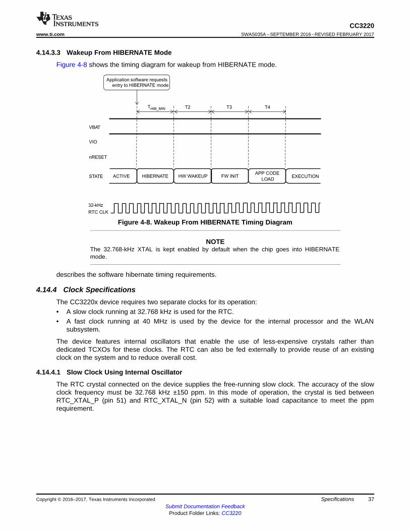
4.14.3.3 Wakeup From HIBERNATE Mode
Figure 4-8 shows the timing diagram for wakeup from HIBERNATE mode.
Figure 4-8. Wakeup From HIBERNATE Timing Diagram
NOTEThe 32.768-kHz XTAL is kept enabled by default when the chip goes into HIBERNATEmode.
describes the software hibernate timing requirements.
4.14.4 Clock SpecificationsThe CC3220x device requires two separate clocks for its operation:• A slow clock running at 32.768 kHz is used for the RTC.• A fast clock running at 40 MHz is used by the device for the internal processor and the WLAN
subsystem.
The device features internal oscillators that enable the use of less-expensive crystals rather thandedicated TCXOs for these clocks. The RTC can also be fed externally to provide reuse of an existingclock on the system and to reduce overall cost.
4.14.4.1 Slow Clock Using Internal Oscillator
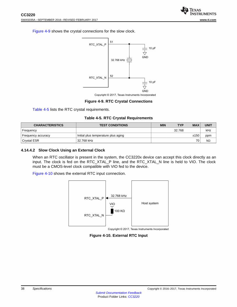
The RTC crystal connected on the device supplies the free-running slow clock. The accuracy of the slowclock frequency must be 32.768 kHz ±150 ppm. In this mode of operation, the crystal is tied betweenRTC_XTAL_P (pin 51) and RTC_XTAL_N (pin 52) with a suitable load capacitance to meet the ppmrequirement.
RTC_XTAL_P
RTC_XTAL_N
Host system
32.768 kHz
VIO
100 KΩ
Copyright © 2017, Texas Instruments Incorporated
RTC_XTAL_P
RTC_XTAL_N
51
52
32.768 kHz
10 pF
GND
GND
10 pF
Copyright © 2017, Texas Instruments Incorporated
38
CC3220SWAS035A –SEPTEMBER 2016–REVISED FEBRUARY 2017 www.ti.com
Submit Documentation FeedbackProduct Folder Links: CC3220
Specifications Copyright © 2016–2017, Texas Instruments Incorporated
Figure 4-9 shows the crystal connections for the slow clock.
Figure 4-9. RTC Crystal Connections
Table 4-5 lists the RTC crystal requirements.
Table 4-5. RTC Crystal Requirements
CHARACTERISTICS TEST CONDITIONS MIN TYP MAX UNITFrequency 32.768 kHzFrequency accuracy Initial plus temperature plus aging ±150 ppmCrystal ESR 32.768 kHz 70 kΩ
4.14.4.2 Slow Clock Using an External Clock
When an RTC oscillator is present in the system, the CC3220x device can accept this clock directly as aninput. The clock is fed on the RTC_XTAL_P line, and the RTC_XTAL_N line is held to VIO. The clockmust be a CMOS-level clock compatible with VIO fed to the device.
Figure 4-10 shows the external RTC input connection.
Figure 4-10. External RTC Input
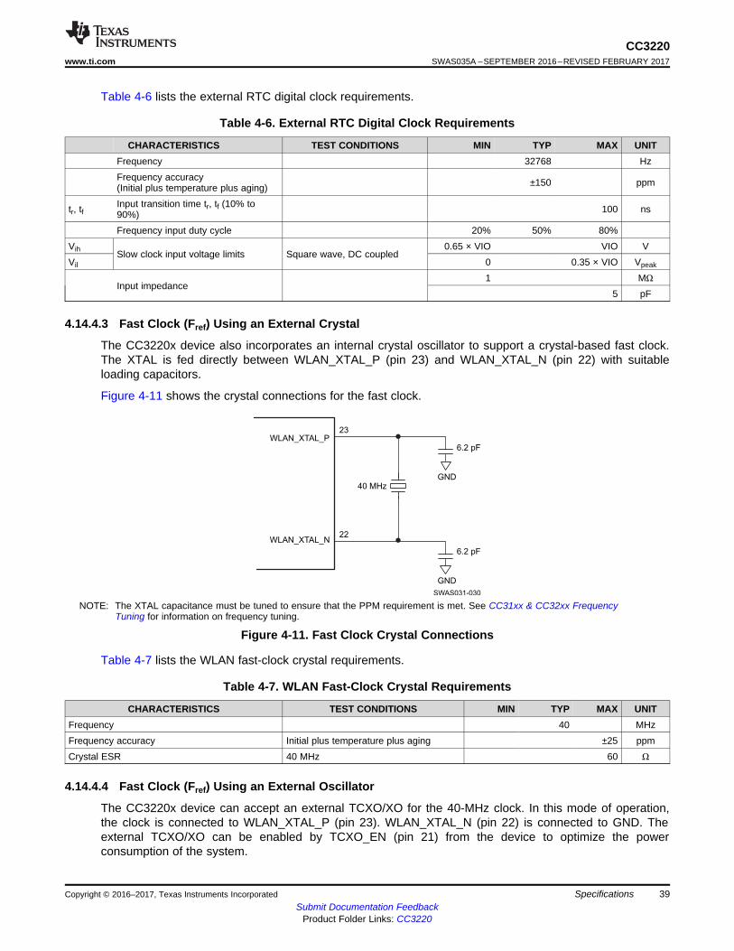
WLAN_XTAL_P
WLAN_XTAL_N
23
22
40 MHzGND
GND
6.2 pF
6.2 pF
SWAS031-030
39
CC3220www.ti.com SWAS035A –SEPTEMBER 2016–REVISED FEBRUARY 2017
Submit Documentation FeedbackProduct Folder Links: CC3220
SpecificationsCopyright © 2016–2017, Texas Instruments Incorporated
Table 4-6 lists the external RTC digital clock requirements.
Table 4-6. External RTC Digital Clock Requirements
CHARACTERISTICS TEST CONDITIONS MIN TYP MAX UNITFrequency 32768 HzFrequency accuracy(Initial plus temperature plus aging) ±150 ppm
tr, tfInput transition time tr, tf (10% to90%) 100 ns
Frequency input duty cycle 20% 50% 80%Vih Slow clock input voltage limits Square wave, DC coupled
0.65 × VIO VIO VVil 0 0.35 × VIO Vpeak
Input impedance1 MΩ
5 pF
4.14.4.3 Fast Clock (Fref) Using an External Crystal
The CC3220x device also incorporates an internal crystal oscillator to support a crystal-based fast clock.The XTAL is fed directly between WLAN_XTAL_P (pin 23) and WLAN_XTAL_N (pin 22) with suitableloading capacitors.
Figure 4-11 shows the crystal connections for the fast clock.
NOTE: The XTAL capacitance must be tuned to ensure that the PPM requirement is met. See CC31xx & CC32xx FrequencyTuning for information on frequency tuning.
Figure 4-11. Fast Clock Crystal Connections
Table 4-7 lists the WLAN fast-clock crystal requirements.
Table 4-7. WLAN Fast-Clock Crystal Requirements
CHARACTERISTICS TEST CONDITIONS MIN TYP MAX UNITFrequency 40 MHzFrequency accuracy Initial plus temperature plus aging ±25 ppmCrystal ESR 40 MHz 60 Ω
4.14.4.4 Fast Clock (Fref) Using an External Oscillator
The CC3220x device can accept an external TCXO/XO for the 40-MHz clock. In this mode of operation,the clock is connected to WLAN_XTAL_P (pin 23). WLAN_XTAL_N (pin 22) is connected to GND. Theexternal TCXO/XO can be enabled by TCXO_EN (pin 21) from the device to optimize the powerconsumption of the system.
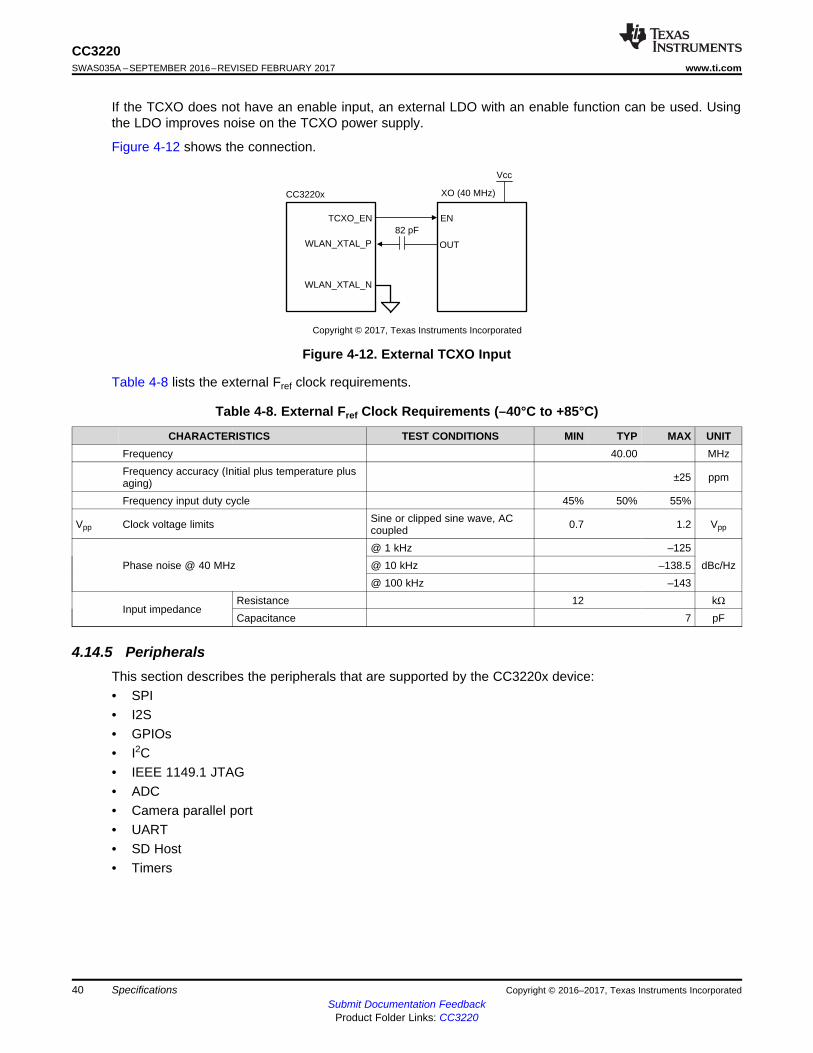
WLAN_XTAL_P
WLAN_XTAL_N
XO (40 MHz)
82 pFTCXO_EN EN
OUT
Vcc
CC3220x
Copyright © 2017, Texas Instruments Incorporated
40
CC3220SWAS035A –SEPTEMBER 2016–REVISED FEBRUARY 2017 www.ti.com
Submit Documentation FeedbackProduct Folder Links: CC3220
Specifications Copyright © 2016–2017, Texas Instruments Incorporated
If the TCXO does not have an enable input, an external LDO with an enable function can be used. Usingthe LDO improves noise on the TCXO power supply.
Figure 4-12 shows the connection.
Figure 4-12. External TCXO Input
Table 4-8 lists the external Fref clock requirements.
Table 4-8. External Fref Clock Requirements (–40°C to +85°C)
CHARACTERISTICS TEST CONDITIONS MIN TYP MAX UNITFrequency 40.00 MHzFrequency accuracy (Initial plus temperature plusaging) ±25 ppm
Frequency input duty cycle 45% 50% 55%
Vpp Clock voltage limits Sine or clipped sine wave, ACcoupled 0.7 1.2 Vpp
Phase noise @ 40 MHz@ 1 kHz –125
dBc/Hz@ 10 kHz –138.5@ 100 kHz –143
Input impedanceResistance 12 kΩCapacitance 7 pF
4.14.5 PeripheralsThis section describes the peripherals that are supported by the CC3220x device:• SPI• I2S• GPIOs• I2C• IEEE 1149.1 JTAG• ADC• Camera parallel port• UART• SD Host• Timers
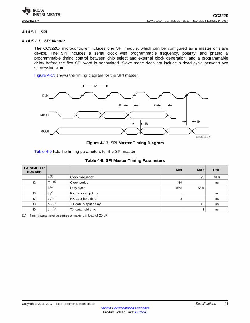
I2
I6 I7
I9
SWAS032-017
CLK
MISO
MOSI
I8
41
CC3220www.ti.com SWAS035A –SEPTEMBER 2016–REVISED FEBRUARY 2017
Submit Documentation FeedbackProduct Folder Links: CC3220
SpecificationsCopyright © 2016–2017, Texas Instruments Incorporated
(1) Timing parameter assumes a maximum load of 20 pF.
4.14.5.1 SPI
4.14.5.1.1 SPI Master
The CC3220x microcontroller includes one SPI module, which can be configured as a master or slavedevice. The SPI includes a serial clock with programmable frequency, polarity, and phase; aprogrammable timing control between chip select and external clock generation; and a programmabledelay before the first SPI word is transmitted. Slave mode does not include a dead cycle between twosuccessive words.
Figure 4-13 shows the timing diagram for the SPI master.
Figure 4-13. SPI Master Timing Diagram
Table 4-9 lists the timing parameters for the SPI master.
Table 4-9. SPI Master Timing Parameters
PARAMETERNUMBER MIN MAX UNIT
F (1) Clock frequency 20 MHzI2 Tclk
(1) Clock period 50 nsD (1) Duty cycle 45% 55%
I6 tIS(1) RX data setup time 1 nsI7 tIH(1) RX data hold time 2 nsI8 tOD
(1) TX data output delay 8.5 nsI9 tOH
(1) TX data hold time 8 ns
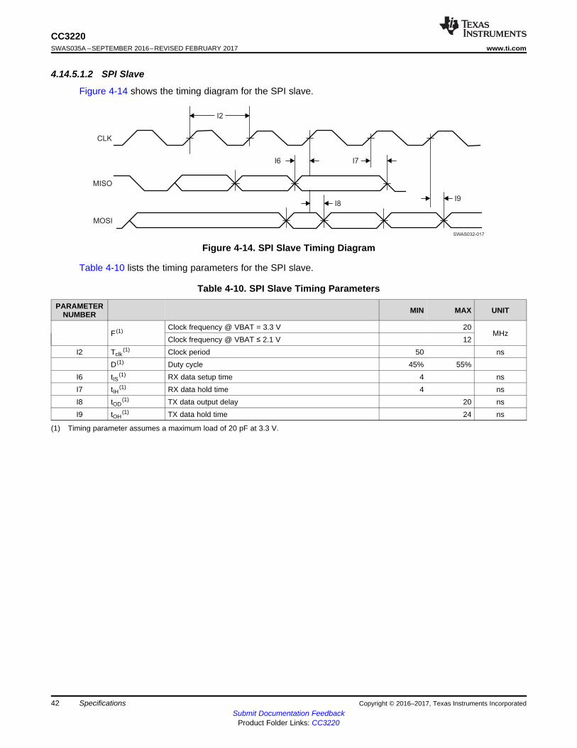
I2
I6 I7
I9
SWAS032-017
CLK
MISO
MOSI
I8
42
CC3220SWAS035A –SEPTEMBER 2016–REVISED FEBRUARY 2017 www.ti.com
Submit Documentation FeedbackProduct Folder Links: CC3220
Specifications Copyright © 2016–2017, Texas Instruments Incorporated
(1) Timing parameter assumes a maximum load of 20 pF at 3.3 V.
4.14.5.1.2 SPI Slave
Figure 4-14 shows the timing diagram for the SPI slave.
Figure 4-14. SPI Slave Timing Diagram
Table 4-10 lists the timing parameters for the SPI slave.
Table 4-10. SPI Slave Timing Parameters
PARAMETERNUMBER MIN MAX UNIT
F (1) Clock frequency @ VBAT = 3.3 V 20MHz
Clock frequency @ VBAT ≤ 2.1 V 12I2 Tclk
(1) Clock period 50 nsD (1) Duty cycle 45% 55%
I6 tIS(1) RX data setup time 4 nsI7 tIH(1) RX data hold time 4 nsI8 tOD
(1) TX data output delay 20 nsI9 tOH
(1) TX data hold time 24 ns
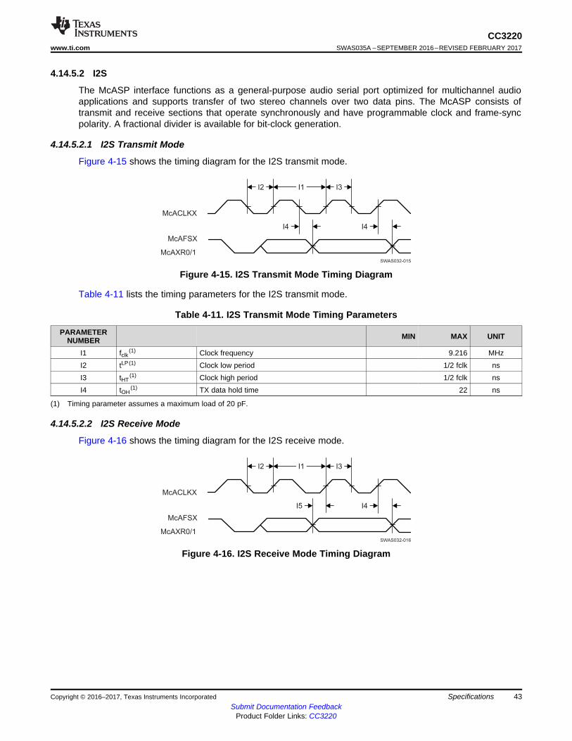
I2 I1 I3
I4
McACLKX
McAFSX
McAXR0/1
SWAS032-016
I5
I2 I1 I3
I4
McACLKX
McAFSX
McAXR0/1
SWAS032-015
I4
43
CC3220www.ti.com SWAS035A –SEPTEMBER 2016–REVISED FEBRUARY 2017
Submit Documentation FeedbackProduct Folder Links: CC3220
SpecificationsCopyright © 2016–2017, Texas Instruments Incorporated
(1) Timing parameter assumes a maximum load of 20 pF.
4.14.5.2 I2S
The McASP interface functions as a general-purpose audio serial port optimized for multichannel audioapplications and supports transfer of two stereo channels over two data pins. The McASP consists oftransmit and receive sections that operate synchronously and have programmable clock and frame-syncpolarity. A fractional divider is available for bit-clock generation.
4.14.5.2.1 I2S Transmit Mode
Figure 4-15 shows the timing diagram for the I2S transmit mode.
Figure 4-15. I2S Transmit Mode Timing Diagram
Table 4-11 lists the timing parameters for the I2S transmit mode.
Table 4-11. I2S Transmit Mode Timing Parameters
PARAMETERNUMBER MIN MAX UNIT
I1 fclk(1) Clock frequency 9.216 MHz
I2 tLP(1) Clock low period 1/2 fclk nsI3 tHT
(1) Clock high period 1/2 fclk nsI4 tOH
(1) TX data hold time 22 ns
4.14.5.2.2 I2S Receive Mode
Figure 4-16 shows the timing diagram for the I2S receive mode.
Figure 4-16. I2S Receive Mode Timing Diagram
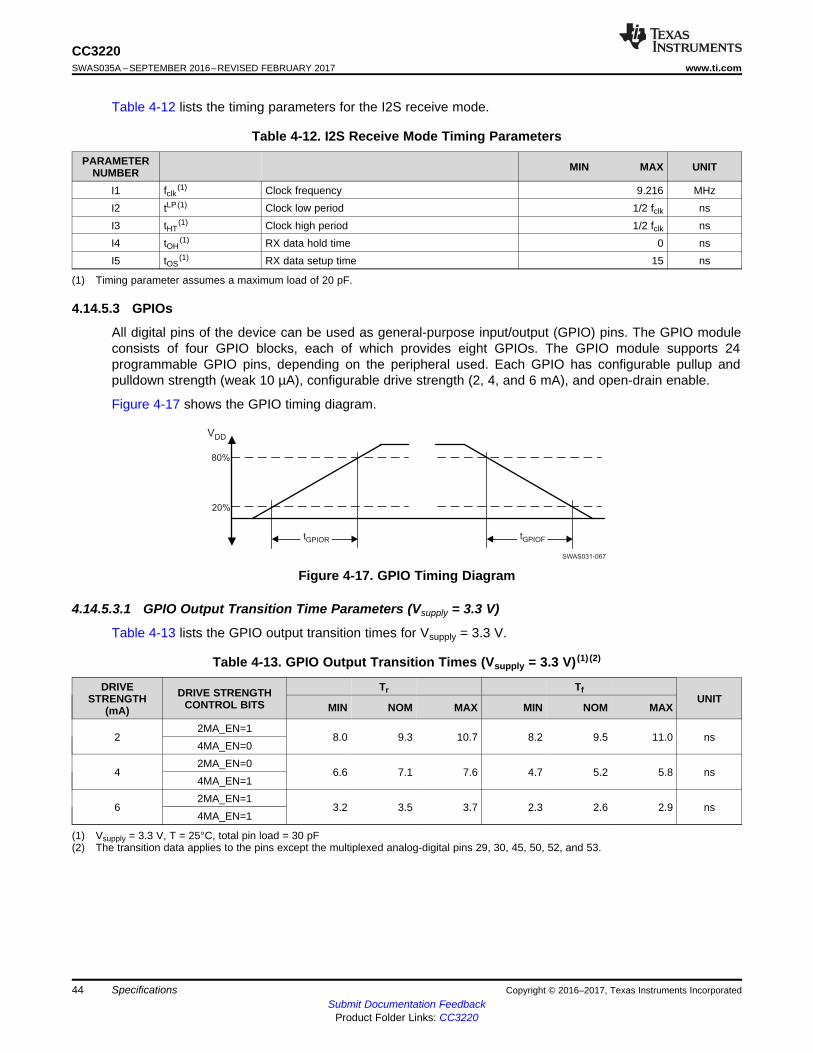
SWAS031-067
VDD
80%
20%
tGPIOFt
GPIOR
44
CC3220SWAS035A –SEPTEMBER 2016–REVISED FEBRUARY 2017 www.ti.com
Submit Documentation FeedbackProduct Folder Links: CC3220
Specifications Copyright © 2016–2017, Texas Instruments Incorporated
(1) Timing parameter assumes a maximum load of 20 pF.
Table 4-12 lists the timing parameters for the I2S receive mode.
Table 4-12. I2S Receive Mode Timing Parameters
PARAMETERNUMBER MIN MAX UNIT
I1 fclk(1) Clock frequency 9.216 MHz
I2 tLP(1) Clock low period 1/2 fclk nsI3 tHT
(1) Clock high period 1/2 fclk nsI4 tOH
(1) RX data hold time 0 nsI5 tOS
(1) RX data setup time 15 ns
(1) Vsupply = 3.3 V, T = 25°C, total pin load = 30 pF(2) The transition data applies to the pins except the multiplexed analog-digital pins 29, 30, 45, 50, 52, and 53.
4.14.5.3 GPIOs
All digital pins of the device can be used as general-purpose input/output (GPIO) pins. The GPIO moduleconsists of four GPIO blocks, each of which provides eight GPIOs. The GPIO module supports 24programmable GPIO pins, depending on the peripheral used. Each GPIO has configurable pullup andpulldown strength (weak 10 µA), configurable drive strength (2, 4, and 6 mA), and open-drain enable.
Figure 4-17 shows the GPIO timing diagram.
Figure 4-17. GPIO Timing Diagram
4.14.5.3.1 GPIO Output Transition Time Parameters (Vsupply = 3.3 V)
Table 4-13 lists the GPIO output transition times for Vsupply = 3.3 V.
Table 4-13. GPIO Output Transition Times (Vsupply = 3.3 V) (1) (2)
DRIVESTRENGTH
(mA)DRIVE STRENGTH
CONTROL BITSTr Tf
UNITMIN NOM MAX MIN NOM MAX
22MA_EN=1
8.0 9.3 10.7 8.2 9.5 11.0 ns4MA_EN=0
42MA_EN=0
6.6 7.1 7.6 4.7 5.2 5.8 ns4MA_EN=1
62MA_EN=1
3.2 3.5 3.7 2.3 2.6 2.9 ns4MA_EN=1
I2 I6 I5
I9I3I8I7I4I1
I2CSCL
I2CSDA
SWAS031-068
45
CC3220www.ti.com SWAS035A –SEPTEMBER 2016–REVISED FEBRUARY 2017
Submit Documentation FeedbackProduct Folder Links: CC3220
SpecificationsCopyright © 2016–2017, Texas Instruments Incorporated
(1) Vsupply = 1.8 V, T = 25°C, total pin load = 30 pF(2) The transition data applies to the pins other than the multiplexed analog-digital pins 29, 30, 45, 50, 52, and 53.
4.14.5.3.2 GPIO Output Transition Time Parameters (Vsupply = 1.85 V)
Table 4-14 lists the GPIO output transition times for Vsupply = 1.8 V.
Table 4-14. GPIO Output Transition Times (Vsupply = 1.85 V) (1) (2)
DRIVESTRENGTH
(mA)DRIVE STRENGTH
CONTROL BITSTr Tf
UNITMIN NOM MAX MIN NOM MAX
22MA_EN=1
11.7 13.9 16.3 11.5 13.9 16.7 ns4MA_EN=0
42MA_EN=0
13.7 15.6 18.0 9.9 11.6 13.6 ns4MA_EN=1
62MA_EN=1
5.5 6.4 7.4 3.8 4.7 5.8 ns4MA_EN=1
4.14.5.3.3 GPIO Input Transition Time Parameters
Table 4-15 lists the input transition time parameters.
Table 4-15. GPIO Input Transition Time Parameters
MIN MAX UNITtr Input transition time (tr, tf), 10% to 90%
1 3 nstf 1 3 ns
4.14.5.4 I2C
The CC3220x microcontroller includes one I2C module operating with standard (100 kbps) or fast(400 kbps) transmission speeds.
Figure 4-18 shows the I2C timing diagram.
Figure 4-18. I2C Timing Diagram
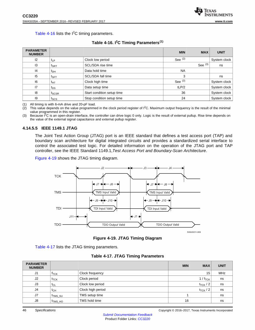
J2 J3 J4
J7 J8 J7 J8
J9 J10 J9 J10
J1J11
TDI Input Valid
TDO Output ValidTDO Output Valid
TMS Input Valid
TDI Input Valid
TCK
TMS
TDI
TDO
SWAS031-069
TMS Input Valid
46
CC3220SWAS035A –SEPTEMBER 2016–REVISED FEBRUARY 2017 www.ti.com
Submit Documentation FeedbackProduct Folder Links: CC3220
Specifications Copyright © 2016–2017, Texas Instruments Incorporated
(1) All timing is with 6-mA drive and 20-pF load.(2) This value depends on the value programmed in the clock period register of I2C. Maximum output frequency is the result of the minimal
value programmed in this register.(3) Because I2C is an open-drain interface, the controller can drive logic 0 only. Logic is the result of external pullup. Rise time depends on
the value of the external signal capacitance and external pullup register.
Table 4-16 lists the I2C timing parameters.
Table 4-16. I2C Timing Parameters (1)
PARAMETERNUMBER MIN MAX UNIT
I2 tLP Clock low period See (2) System clockI3 tSRT SCL/SDA rise time See (3) nsI4 tDH Data hold time NAI5 tSFT SCL/SDA fall time 3 nsI6 tHT Clock high time See (2) System clockI7 tDS Data setup time tLP/2 System clockI8 tSCSR Start condition setup time 36 System clockI9 tSCS Stop condition setup time 24 System clock
4.14.5.5 IEEE 1149.1 JTAG
The Joint Test Action Group (JTAG) port is an IEEE standard that defines a test access port (TAP) andboundary scan architecture for digital integrated circuits and provides a standardized serial interface tocontrol the associated test logic. For detailed information on the operation of the JTAG port and TAPcontroller, see the IEEE Standard 1149.1,Test Access Port and Boundary-Scan Architecture.
Figure 4-19 shows the JTAG timing diagram.
Figure 4-19. JTAG Timing Diagram
Table 4-17 lists the JTAG timing parameters.
Table 4-17. JTAG Timing Parameters
PARAMETERNUMBER MIN MAX UNIT
J1 fTCK Clock frequency 15 MHzJ2 tTCK Clock period 1 / fTCK nsJ3 tCL Clock low period tTCK / 2 nsJ4 tCH Clock high period tTCK / 2 nsJ7 tTMS_SU TMS setup time 1 nsJ8 tTMS_HO TMS hold time 16 ns
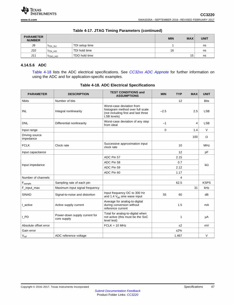
47
CC3220www.ti.com SWAS035A –SEPTEMBER 2016–REVISED FEBRUARY 2017
Submit Documentation FeedbackProduct Folder Links: CC3220
SpecificationsCopyright © 2016–2017, Texas Instruments Incorporated
Table 4-17. JTAG Timing Parameters (continued)PARAMETER
NUMBER MIN MAX UNIT
J9 tTDI_SU TDI setup time 1 nsJ10 tTDI_HO TDI hold time 16 nsJ11 tTDO_HO TDO hold time 15 ns
4.14.5.6 ADC
Table 4-18 lists the ADC electrical specifications. See CC32xx ADC Appnote for further information onusing the ADC and for application-specific examples.
Table 4-18. ADC Electrical Specifications
PARAMETER DESCRIPTION TEST CONDITIONS andASSUMPTIONS MIN TYP MAX UNIT
Nbits Number of bits 12 Bits
INL Integral nonlinearity
Worst-case deviation fromhistogram method over full scale(not including first and last threeLSB levels)
–2.5 2.5 LSB
DNL Differential nonlinearity Worst-case deviation of any stepfrom ideal –1 4 LSB
Input range 0 1.4 VDriving sourceimpedance 100 Ω
FCLK Clock rate Successive approximation inputclock rate 10 MHz
Input capacitance 12 pF
Input impedance
ADC Pin 57 2.15
kΩADC Pin 58 0.7ADC Pin 59 2.12ADC Pin 60 1.17
Number of channels 4Fsample Sampling rate of each pin 62.5 KSPSF_input_max Maximum input signal frequency 31 kHz
SINAD Signal-to-noise and distortion Input frequency DC to 300 Hzand 1.4 Vpp sine wave input 55 60 dB
I_active Active supply currentAverage for analog-to-digitalduring conversion withoutreference current
1.5 mA
I_PD Power-down supply current forcore supply
Total for analog-to-digital whennot active (this must be the SoClevel test)
1 µA
Absolute offset error FCLK = 10 MHz ±2 mVGain error ±2%Vref ADC reference voltage 1.467 V
pCLK
pVS, pHS
pDATA
13 12 14
16 17
2 µs 2 µs 2 µs 2 µs 2 µs 2 µs 2 µs 2 µs 2 µs 2 µs
Repeats Every 16 µs
ADC CLOCK= 10 MHz
Sampling4 cycles
SAR Conversion16 cycles
Sampling4 cycles
SAR Conversion16 cycles
Sampling4 cycles
SAR Conversion16 cycles
Sampling4 cycles
SAR Conversion16 cycles
EXT CHANNEL 0 INTERNAL CHANNEL EXT CHANNEL 1 INTERNAL CHANNEL
Internal Ch
48
CC3220SWAS035A –SEPTEMBER 2016–REVISED FEBRUARY 2017 www.ti.com
Submit Documentation FeedbackProduct Folder Links: CC3220
Specifications Copyright © 2016–2017, Texas Instruments Incorporated
Figure 4-20 shows the ADC clock timing diagram.
Figure 4-20. ADC Clock Timing Diagram
4.14.5.7 Camera Parallel Port
The fast camera parallel port interfaces with a variety of external image sensors, stores the image data ina FIFO, and generates DMA requests. The camera parallel port supports 8 bits.
Figure 4-21 shows the timing diagram for the camera parallel port.
Figure 4-21. Camera Parallel Port Timing Diagram
Table 4-19 lists the timing parameters for the camera parallel port.
Table 4-19. Camera Parallel Port Timing Parameters
PARAMETER NUMBER MIN MAX UNITpCLK Clock frequency 2 MHz
I2 Tclk Clock period 1/pCLK nsI3 tLP Clock low period Tclk/2 nsI4 tHT Clock high period Tclk/2 nsI6 tIS RX data setup time 2 nsI7 tIH RX data hold time 2 ns
D Duty cycle 45% 55%
4.14.5.8 UART
The CC3220x device includes two UARTs with the following features:• Programmable baud-rate generator allowing speeds up to 3 Mbps• Separate 16-bit × 8-bit TX and RX FIFOs to reduce CPU interrupt service loading• Programmable FIFO length, including a 1-byte-deep operation providing conventional double-buffered
interface• FIFO trigger levels of 1/8, 1/4, 1/2, 3/4, and 7/8• Standard asynchronous communication bits for start, stop, and parity• Generation and detection of line-breaks

49
CC3220www.ti.com SWAS035A –SEPTEMBER 2016–REVISED FEBRUARY 2017
Submit Documentation FeedbackProduct Folder Links: CC3220
SpecificationsCopyright © 2016–2017, Texas Instruments Incorporated
• Fully programmable serial interface characteristics:– 5, 6, 7, or 8 data bits– Generation and detection of even, odd, stick, or no-parity bits– Generation of 1 or 2 stop-bits
• RTS and CTS hardware flow support• Standard FIFO-level and End-of-Transmission interrupts• Efficient transfers using µDMA:
– Separate channels for transmit and receive– Receive single request asserted when data is in the FIFO; burst request asserted at programmed
FIFO level– Transmit single request asserted when there is space in the FIFO; burst request asserted at
programmed FIFO level• System clock is used to generate the baud clock.
4.14.5.9 SD Host
CC3220x provides an interface between a local host (LH), such as an MCU and an SD memory card, andhandles SD transactions with minimal LH intervention.
The SD host does the following:• Provides SD card access in 1-bit mode• Deals with SD protocol at the transmission level• Handles data packing• Adds cyclic redundancy checks (CRC)• Start and end bit• Checks for syntactical correctness
The application interface sends every SD command and either polls for the status of the adapter or waitsfor an interrupt request. The result is then sent back to the application interface in case of exceptions or towarn of end-of-operation. The controller can be configured to generate DMA requests and work withminimum CPU intervention. Given the nature of integration of this peripheral on the CC3220x platform, TIrecommends that developers use peripheral library APIs to control and operate the block. This sectionemphasizes understanding the SD host APIs provided in the peripheral library of the CC3220x SoftwareDevelopment Kit (SDK).
The SD Host features are as follows:• Full compliance with SD command and response sets, as defined in the SD memory card
– Specifications, v2.0– Includes high-capacity (size >2 GB) cards HC SD
• Flexible architecture, allowing support for new command structure.• 1-bit transfer mode specifications for SD cards• Built-in 1024-byte buffer for read or write
– 512-byte buffer for both transmit and receive– Each buffer is 32-bits wide by 128-words deep
• 32-bit-wide access bus to maximize bus throughput• Single interrupt line for multiple interrupt source events• Two slave DMA channels (1 for TX, 1 for RX)• Programmable clock generation• Integrates an internal transceiver that allows a direct connection to the SD card without external
transceiver• Supports configurable busy and response timeout
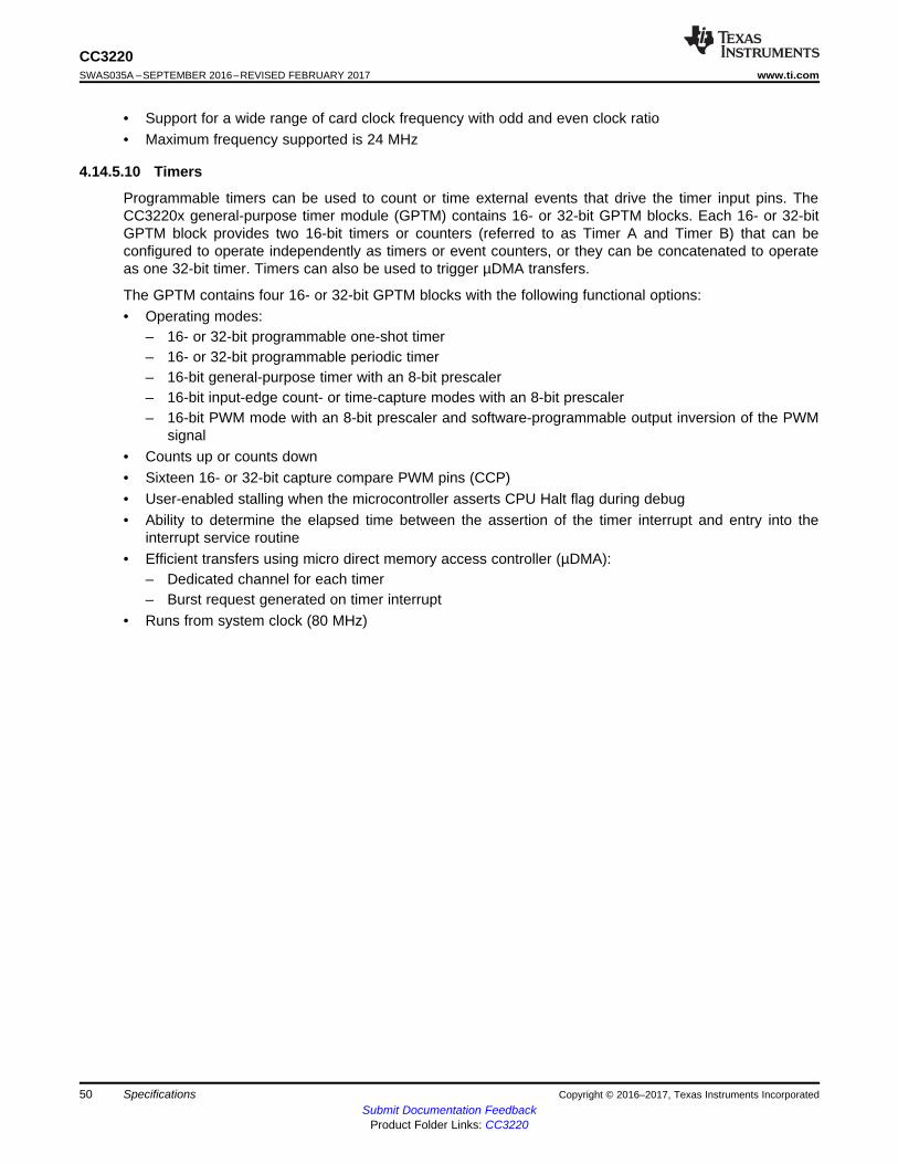
50
CC3220SWAS035A –SEPTEMBER 2016–REVISED FEBRUARY 2017 www.ti.com
Submit Documentation FeedbackProduct Folder Links: CC3220
Specifications Copyright © 2016–2017, Texas Instruments Incorporated
• Support for a wide range of card clock frequency with odd and even clock ratio• Maximum frequency supported is 24 MHz
4.14.5.10 Timers
Programmable timers can be used to count or time external events that drive the timer input pins. TheCC3220x general-purpose timer module (GPTM) contains 16- or 32-bit GPTM blocks. Each 16- or 32-bitGPTM block provides two 16-bit timers or counters (referred to as Timer A and Timer B) that can beconfigured to operate independently as timers or event counters, or they can be concatenated to operateas one 32-bit timer. Timers can also be used to trigger µDMA transfers.
The GPTM contains four 16- or 32-bit GPTM blocks with the following functional options:• Operating modes:
– 16- or 32-bit programmable one-shot timer– 16- or 32-bit programmable periodic timer– 16-bit general-purpose timer with an 8-bit prescaler– 16-bit input-edge count- or time-capture modes with an 8-bit prescaler– 16-bit PWM mode with an 8-bit prescaler and software-programmable output inversion of the PWM
signal• Counts up or counts down• Sixteen 16- or 32-bit capture compare PWM pins (CCP)• User-enabled stalling when the microcontroller asserts CPU Halt flag during debug• Ability to determine the elapsed time between the assertion of the timer interrupt and entry into the
interrupt service routine• Efficient transfers using micro direct memory access controller (µDMA):
– Dedicated channel for each timer– Burst request generated on timer interrupt
• Runs from system clock (80 MHz)
Wide voltage
(2.1 to 3.6 V)/preregulated 1.85 V
Miscellaneousperipheral
Camerasensor
SSPI GSPI
Audiocodec
GPIO/PWMParallel
port I2S
CC3220x
I2C
Copyright © 2017, Texas Instruments Incorporated
VCC
40-MHzXTAL
32-kHzXTAL
SPIFlash
SPIperipheral
I2Cperipheral
51
CC3220www.ti.com SWAS035A –SEPTEMBER 2016–REVISED FEBRUARY 2017
Submit Documentation FeedbackProduct Folder Links: CC3220
Detailed DescriptionCopyright © 2016–2017, Texas Instruments Incorporated
5 Detailed Description
5.1 OverviewThe CC3220x wireless MCU family has a rich set of peripherals for diverse application requirements. Thissection briefly highlights the internal details of the CC3220x devices and offers suggestions for applicationconfigurations.
5.2 Functional Block DiagramFigure 5-1 shows the functional block diagram of the CC3220x SimpleLink Wi-Fi solution.
Figure 5-1. Functional Block Diagram
52
CC3220SWAS035A –SEPTEMBER 2016–REVISED FEBRUARY 2017 www.ti.com
Submit Documentation FeedbackProduct Folder Links: CC3220
Detailed Description Copyright © 2016–2017, Texas Instruments Incorporated
5.3 ARM® Cortex®-M4 Processor Core SubsystemThe high-performance Cortex-M4 processor provides a low-cost platform that meets the needs of minimalmemory implementation, reduced pin count, and low power consumption, while delivering outstandingcomputational performance and exceptional system response to interrupts.• The Cortex-M4 core has low-latency interrupt processing with the following features:
– A 32-bit ARM® Thumb® instruction set optimized for embedded applications– Handler and thread modes– Low-latency interrupt handling by automatic processor state saving and restoration during entry and
exit– Support for ARMv6 unaligned accesses
• Nested vectored interrupt controller (NVIC) closely integrated with the processor core to achieve low-latency interrupt processing. The NVIC includes the following features:– Bits of priority configurable from 3 to 8– Dynamic reprioritization of interrupts– Priority grouping that enables selection of preempting interrupt levels and nonpreempting interrupt
levels– Support for tail-chaining and late arrival of interrupts, which enables back-to-back interrupt
processing without the overhead of state saving and restoration between interrupts– Processor state automatically saved on interrupt entry and restored on interrupt exit with no
instruction overhead– Wake-up interrupt controller (WIC) providing ultra-low-power sleep mode support
• Bus interfaces:– Advanced high-performance bus (AHB-Lite) interfaces: system bus interfaces– Bit-band support for memory and select peripheral that includes atomic bit-band write and read
operations• Low-cost debug solution featuring:
– Debug access to all memory and registers in the system, including access to memory-mappeddevices, access to internal core registers when the core is halted, and access to debug controlregisters even while SYSRESETn is asserted
– Serial wire debug port (SW-DP) or serial wire JTAG debug port (SWJ-DP) debug access– Flash patch and breakpoint (FPB) unit to implement breakpoints and code patches
5.4 Wi-Fi Network Processor SubsystemThe Wi-Fi network processor subsystem includes a dedicated ARM MCU to completely offload the hostMCU along with an 802.11 b/g/n radio, baseband, and MAC with a powerful crypto engine for a fast,secure WLAN and Internet connections with 256-bit encryption. The CC3220x devices support station, AP,and Wi-Fi Direct modes. The device also supports WPA2 personal and enterprise security and WPS 2.0.The Wi-Fi network processor includes an embedded IPv6, IPv4 TCP/IP stack.
53
CC3220www.ti.com SWAS035A –SEPTEMBER 2016–REVISED FEBRUARY 2017
Submit Documentation FeedbackProduct Folder Links: CC3220
Detailed DescriptionCopyright © 2016–2017, Texas Instruments Incorporated
5.4.1 WLANThe WLAN features are as follows:• 802.11b/g/n integrated radio, modem, and MAC supporting WLAN communication as a BSS station,
AP, Wi-Fi Direct client and group owner with CCK and OFDM rates in the 2.4-GHz ISM band, channels1 to 13.
NOTE802.11n is supported only in Wi-Fi station, Wi-Fi direct, and P2P client modes.
• Autocalibrated radio with a single-ended 50-Ω interface enables easy connection to the antennawithout requiring expertise in radio circuit design.
• Advanced connection manager with multiple user-configurable profiles stored in serial-flash allowsautomatic fast connection to an access point without user or host intervention.
• Supports all common Wi-Fi security modes for personal and enterprise networks with on-chip securityaccelerators, including: WEP, WPA/WPA2 PSK, WPA2 Enterprise (802.1x).
• Smart provisioning options deeply integrated within the device providing a comprehensive end-to-endsolution. With elaborate events notification to the host, enabling the application to control theprovisioning decision flow. The wide variety of Wi-Fi provisioning methods include:– Access Point using HTTPS– SmartConfig Technology: a 1-step, 1-time process to connect a CC3220-enabled device to the
home wireless network, removing dependency on the I/O capabilities of the host MCU; thus, it isusable by deeply embedded applications
• 802.11 transceiver mode allows transmitting and receiving of proprietary data through a socket withoutadding MAC or PHY headers. The 802.11 transceiver mode provides the option to select the workingchannel, rate, and transmitted power. The receiver mode works with the filtering options.
5.4.2 Network StackThe Network Stack features are as follows:• Integrated IPv4, IPv6 TCP/IP stack with BSD (BSD adjacent) socket APIs for simple Internet
connectivity with any MCU, microprocessor, or ASIC
NOTENot all APIs are 100% BSD compliant. Not all BSD APIs are supported.
• Support of 16 simultaneous TCP, UDP, or RAW sockets• Support of 6 simultaneous SSL\TLS sockets• Built-in network protocols:
– Static IP, LLA, DHCPv4, DHCPv6 with DAD and stateless autoconfiguration– ARP, ICMPv4, IGMP, ICMPv6, MLD, ND– DNS client for easy connection to the local network and the Internet
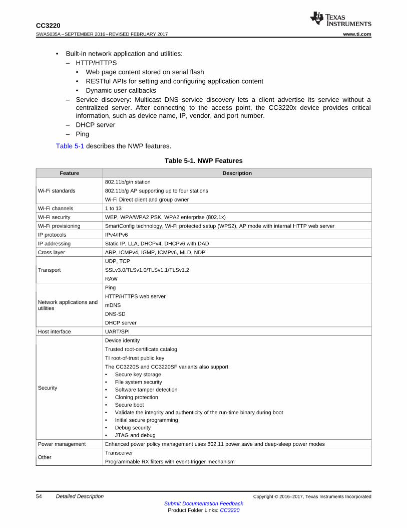
54
CC3220SWAS035A –SEPTEMBER 2016–REVISED FEBRUARY 2017 www.ti.com
Submit Documentation FeedbackProduct Folder Links: CC3220
Detailed Description Copyright © 2016–2017, Texas Instruments Incorporated
• Built-in network application and utilities:– HTTP/HTTPS
• Web page content stored on serial flash• RESTful APIs for setting and configuring application content• Dynamic user callbacks
– Service discovery: Multicast DNS service discovery lets a client advertise its service without acentralized server. After connecting to the access point, the CC3220x device provides criticalinformation, such as device name, IP, vendor, and port number.
– DHCP server– Ping
Table 5-1 describes the NWP features.
Table 5-1. NWP Features
Feature Description
Wi-Fi standards802.11b/g/n station802.11b/g AP supporting up to four stationsWi-Fi Direct client and group owner
Wi-Fi channels 1 to 13Wi-Fi security WEP, WPA/WPA2 PSK, WPA2 enterprise (802.1x)Wi-Fi provisioning SmartConfig technology, Wi-Fi protected setup (WPS2), AP mode with internal HTTP web serverIP protocols IPv4/IPv6IP addressing Static IP, LLA, DHCPv4, DHCPv6 with DADCross layer ARP, ICMPv4, IGMP, ICMPv6, MLD, NDP
TransportUDP, TCPSSLv3.0/TLSv1.0/TLSv1.1/TLSv1.2RAW
Network applications andutilities
PingHTTP/HTTPS web servermDNSDNS-SDDHCP server
Host interface UART/SPI
Security
Device identityTrusted root-certificate catalogTI root-of-trust public keyThe CC3220S and CC3220SF variants also support:• Secure key storage• File system security• Software tamper detection• Cloning protection• Secure boot• Validate the integrity and authenticity of the run-time binary during boot• Initial secure programming• Debug security• JTAG and debug
Power management Enhanced power policy management uses 802.11 power save and deep-sleep power modes
OtherTransceiverProgrammable RX filters with event-trigger mechanism
55
CC3220www.ti.com SWAS035A –SEPTEMBER 2016–REVISED FEBRUARY 2017
Submit Documentation FeedbackProduct Folder Links: CC3220
Detailed DescriptionCopyright © 2016–2017, Texas Instruments Incorporated
5.5 SecurityThe SimpleLink Wi-Fi CC3220x Internet-on-a-Chip device enhances the security capabilities available fordevelopment of IoT devices, while completely offloading these activities from the MCU to the networkingsubsystem. The security capabilities include the following key features:
Wi-Fi and Internet Security:• Personal and enterprise Wi-Fi security
– Personal standards• AES (WPA2-PSK)• TKIP (WPA-PSK• WEP
– Enterprise standards• EAP Fast• EAP PEAPv0/1• EAP PEAPv0 TLS• EAP PEAPv1 TLS EAP LS• EAP TLS• EAP TTLS TLS• EAP TTLS MSCHAPv2
56
CC3220SWAS035A –SEPTEMBER 2016–REVISED FEBRUARY 2017 www.ti.com
Submit Documentation FeedbackProduct Folder Links: CC3220
Detailed Description Copyright © 2016–2017, Texas Instruments Incorporated
• Secure sockets– Protocol versions: SSL v3, TLS 1.0, TLS 1.1, TLS 1.2– Powerful crypto engine for fast, secure Wi-Fi and internet connections with 256-bit AES encryption
for TLS and SSL connections– Ciphers suites
• SL_SEC_MASK_SSL_RSA_WITH_RC4_128_SHA• SL_SEC_MASK_SSL_RSA_WITH_RC4_128_MD5• SL_SEC_MASK_TLS_RSA_WITH_AES_256_CBC_SHA• SL_SEC_MASK_TLS_DHE_RSA_WITH_AES_256_CBC_SHA• SL_SEC_MASK_TLS_ECDHE_RSA_WITH_AES_256_CBC_SHA• SL_SEC_MASK_TLS_ECDHE_RSA_WITH_RC4_128_SHA• SL_SEC_MASK_TLS_RSA_WITH_AES_128_CBC_SHA256• SL_SEC_MASK_TLS_RSA_WITH_AES_256_CBC_SHA256• SL_SEC_MASK_TLS_ECDHE_RSA_WITH_AES_128_CBC_SHA256• SL_SEC_MASK_TLS_ECDHE_ECDSA_WITH_AES_128_CBC_SHA256• SL_SEC_MASK_TLS_ECDHE_ECDSA_WITH_AES_128_CBC_SHA• SL_SEC_MASK_TLS_ECDHE_ECDSA_WITH_AES_256_CBC_SHA• SL_SEC_MASK_TLS_RSA_WITH_AES_128_GCM_SHA256• SL_SEC_MASK_TLS_RSA_WITH_AES_256_GCM_SHA384• SL_SEC_MASK_TLS_DHE_RSA_WITH_AES_128_GCM_SHA256• SL_SEC_MASK_TLS_DHE_RSA_WITH_AES_256_GCM_SHA384• SL_SEC_MASK_TLS_ECDHE_RSA_WITH_AES_128_GCM_SHA256• SL_SEC_MASK_TLS_ECDHE_RSA_WITH_AES_256_GCM_SHA384• SL_SEC_MASK_TLS_ECDHE_ECDSA_WITH_AES_128_GCM_SHA256• SL_SEC_MASK_TLS_ECDHE_ECDSA_WITH_AES_256_GCM_SHA384• SL_SEC_MASK_TLS_ECDHE_ECDSA_WITH_CHACHA20_POLY1305_SHA256• SL_SEC_MASK_TLS_ECDHE_RSA_WITH_CHACHA20_POLY1305_SHA256• SL_SEC_MASK_TLS_DHE_RSA_WITH_CHACHA20_POLY1305_SHA256
– Server authentication– Client authentication– Domain name verification– Runtime socket upgrade to secure socket – STARTTLS
• Secure HTTP server (HTTPS)• Trusted root-certificate catalog—Verifies that the CA used by the application is trusted and known
secure content delivery• TI root-of-trust public key—Hardware-based mechanism that allows authenticating TI as the genuine
origin of a given content using asymmetric keys• Secure content delivery—Allows encrypted file transfer to the system using asymmetric keys created
by the device
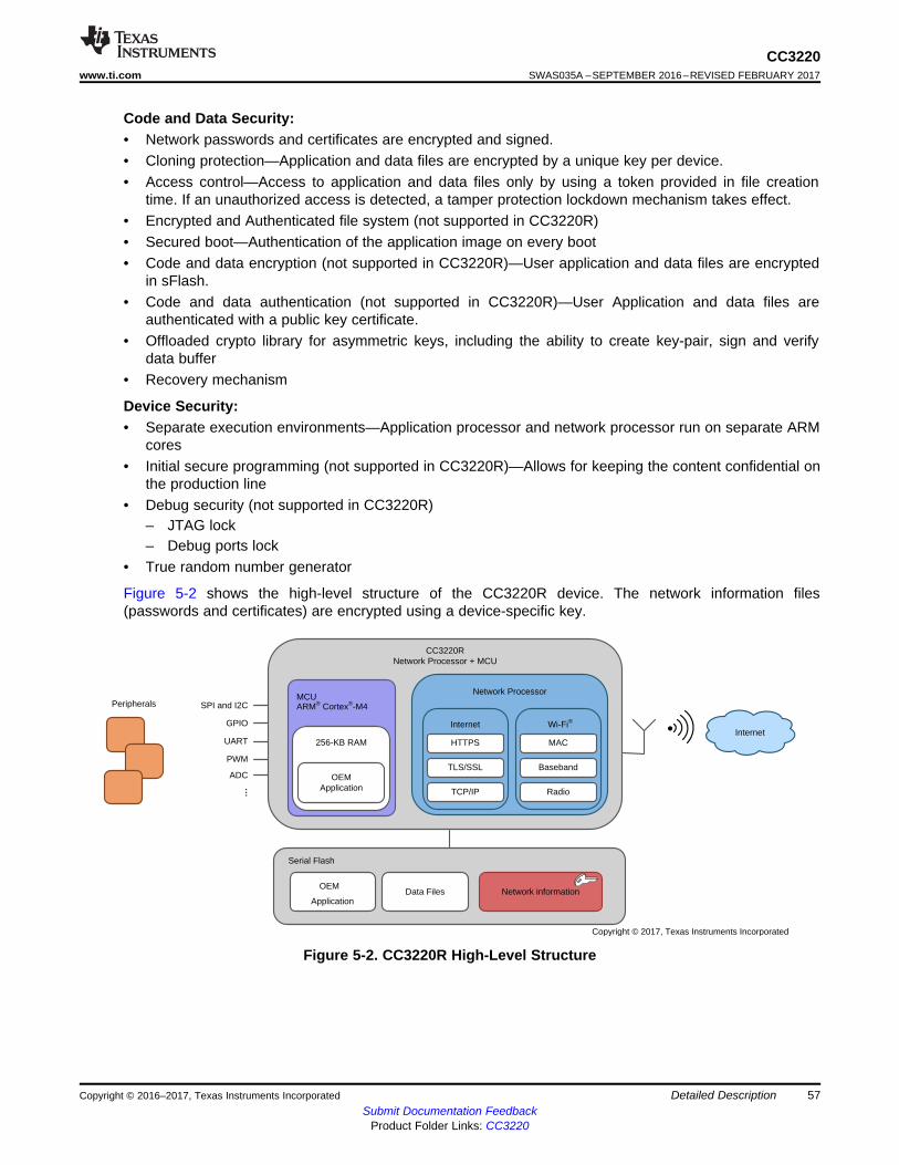
CC3220RNetwork Processor + MCU
Network Processor
Wi-Fi®Internet
Peripherals
OEMApplication
Serial Flash
Data FilesOEM
ApplicationNetwork information
Radio
Baseband
MACHTTPS
TLS/SSL
TCP/IP
MCU ARM® Cortex®-M4
256-KB RAM
SPI and I2C
GPIO
UART
PWM
ADC
Copyright © 2017, Texas Instruments Incorporated
Internet
57
CC3220www.ti.com SWAS035A –SEPTEMBER 2016–REVISED FEBRUARY 2017
Submit Documentation FeedbackProduct Folder Links: CC3220
Detailed DescriptionCopyright © 2016–2017, Texas Instruments Incorporated
Code and Data Security:• Network passwords and certificates are encrypted and signed.• Cloning protection—Application and data files are encrypted by a unique key per device.• Access control—Access to application and data files only by using a token provided in file creation
time. If an unauthorized access is detected, a tamper protection lockdown mechanism takes effect.• Encrypted and Authenticated file system (not supported in CC3220R)• Secured boot—Authentication of the application image on every boot• Code and data encryption (not supported in CC3220R)—User application and data files are encrypted
in sFlash.• Code and data authentication (not supported in CC3220R)—User Application and data files are
authenticated with a public key certificate.• Offloaded crypto library for asymmetric keys, including the ability to create key-pair, sign and verify
data buffer• Recovery mechanism
Device Security:• Separate execution environments—Application processor and network processor run on separate ARM
cores• Initial secure programming (not supported in CC3220R)—Allows for keeping the content confidential on
the production line• Debug security (not supported in CC3220R)
– JTAG lock– Debug ports lock
• True random number generator
Figure 5-2 shows the high-level structure of the CC3220R device. The network information files(passwords and certificates) are encrypted using a device-specific key.
Figure 5-2. CC3220R High-Level Structure
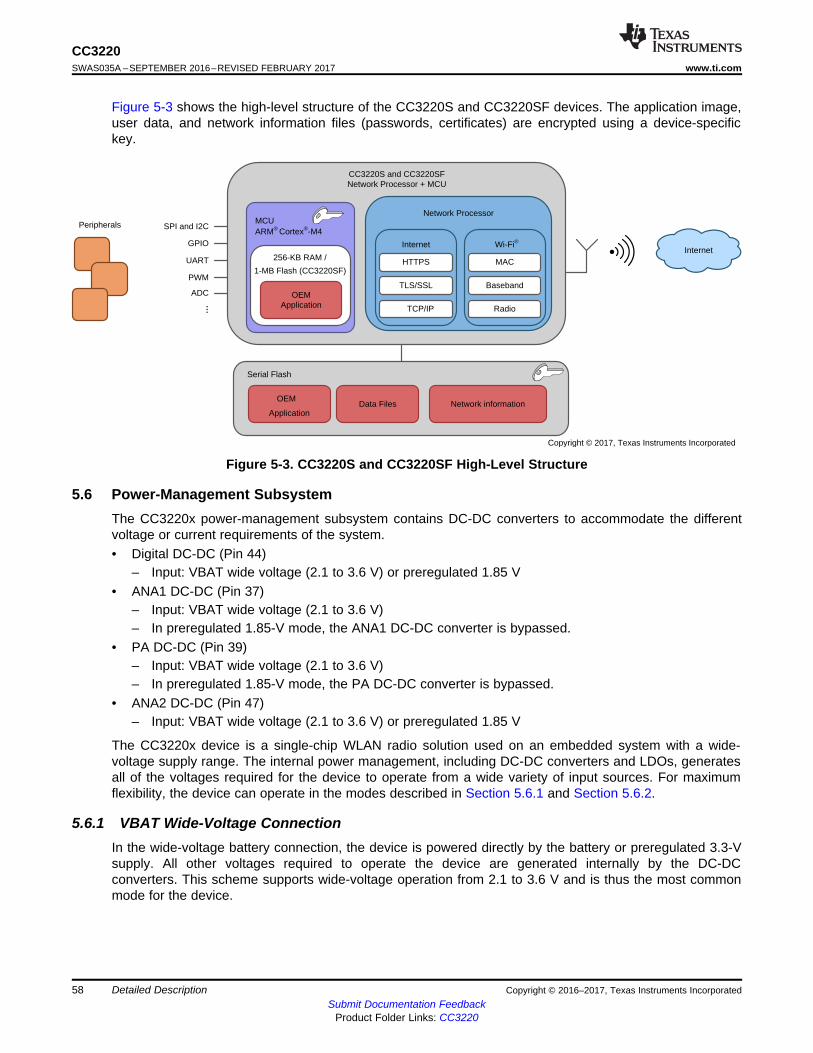
CC3220S and CC3220SFNetwork Processor + MCU
Network Processor
Wi-Fi® Internet
Peripherals
OEMApplication
Serial Flash
Data FilesOEM
ApplicationNetwork information
Radio
Baseband
MACHTTPS
TLS/SSL
TCP/IP
MCU ARM® Cortex®-M4
256-KB RAM /
1-MB Flash (CC3220SF)
SPI and I2C
GPIO
UART
PWM
ADC
Copyright © 2017, Texas Instruments Incorporated
Internet
58
CC3220SWAS035A –SEPTEMBER 2016–REVISED FEBRUARY 2017 www.ti.com
Submit Documentation FeedbackProduct Folder Links: CC3220
Detailed Description Copyright © 2016–2017, Texas Instruments Incorporated
Figure 5-3 shows the high-level structure of the CC3220S and CC3220SF devices. The application image,user data, and network information files (passwords, certificates) are encrypted using a device-specifickey.
Figure 5-3. CC3220S and CC3220SF High-Level Structure
5.6 Power-Management SubsystemThe CC3220x power-management subsystem contains DC-DC converters to accommodate the differentvoltage or current requirements of the system.• Digital DC-DC (Pin 44)
– Input: VBAT wide voltage (2.1 to 3.6 V) or preregulated 1.85 V• ANA1 DC-DC (Pin 37)
– Input: VBAT wide voltage (2.1 to 3.6 V)– In preregulated 1.85-V mode, the ANA1 DC-DC converter is bypassed.
• PA DC-DC (Pin 39)– Input: VBAT wide voltage (2.1 to 3.6 V)– In preregulated 1.85-V mode, the PA DC-DC converter is bypassed.
• ANA2 DC-DC (Pin 47)– Input: VBAT wide voltage (2.1 to 3.6 V) or preregulated 1.85 V
The CC3220x device is a single-chip WLAN radio solution used on an embedded system with a wide-voltage supply range. The internal power management, including DC-DC converters and LDOs, generatesall of the voltages required for the device to operate from a wide variety of input sources. For maximumflexibility, the device can operate in the modes described in Section 5.6.1 and Section 5.6.2.
5.6.1 VBAT Wide-Voltage ConnectionIn the wide-voltage battery connection, the device is powered directly by the battery or preregulated 3.3-Vsupply. All other voltages required to operate the device are generated internally by the DC-DCconverters. This scheme supports wide-voltage operation from 2.1 to 3.6 V and is thus the most commonmode for the device.
59
CC3220www.ti.com SWAS035A –SEPTEMBER 2016–REVISED FEBRUARY 2017
Submit Documentation FeedbackProduct Folder Links: CC3220
Detailed DescriptionCopyright © 2016–2017, Texas Instruments Incorporated
(1) Modes are listed in order of power consumption, with highest power modes listed first.
5.6.2 Preregulated 1.85-V ConnectionThe preregulated 1.85-V mode of operation applies an external regulated 1.85 V directly at pins 10, 25,33, 36, 37, 39, 44, 48, and 54 of the device. The VBAT and the VIO are also connected to the 1.85-Vsupply. This mode provides the lowest BOM count version in which inductors used for PA DC-DC andANA1 DC-DC (2.2 and 1 µH) and a capacitor (22 µF) can be avoided.
In the preregulated 1.85-V mode, the regulator providing the 1.85 V must have the followingcharacteristics:• Load current capacity ≥900 mA• Line and load regulation with <2% ripple with 500-mA step current and settling time of < 4 µs with the
load step
NOTEThe regulator must be placed as close as possible to the device so that the IR drop to thedevice is very low.
5.7 Low-Power Operating ModeFrom a power-management perspective, the CC3220x device comprises the following two independentsubsystems:• Cortex-M4 application processor subsystem• Networking subsystem
Each subsystem operates in one of several power states.
The Cortex-M4 application processor runs the user application loaded from an external serial flash, orinternal flash (in CC3220SF). The networking subsystem runs preprogrammed TCP/IP and Wi-Fi data linklayer functions.
The user program controls the power state of the application processor subsystem and can be in one ofthe five modes described in Table 5-2.
Table 5-2. User Program Modes
APPLICATION PROCESSOR(MCU) MODE (1) DESCRIPTION
MCU active mode MCU executing code at 80-MHz state rate
MCU sleep modeThe MCU clocks are gated off in sleep mode and the entire state of the device is retained. Sleep modeoffers instant wakeup. The MCU can be configured to wake up by an internal fast timer or by activityfrom any GPIO line or peripheral.
MCU LPDS mode
State information is lost and only certain MCU-specific register configurations are retained. The MCUcan wake up from external events or by using an internal timer. (The wake-up time is less than 3 ms.)Certain parts of memory can be retained while the MCU is in LPDS mode. The amount of memoryretained is configurable. Users can choose to preserve code and the MCU-specific setting. The MCUcan be configured to wake up using the RTC timer or by an external event on specific GPIOs defined asthe wake-up source.
MCU hibernate mode
The lowest power mode in which all digital logic is power-gated. Only a small section of the logic directlypowered by the input supply is retained. The RTC keeps running and the MCU supports wakeup froman external event or from an RTC timer expiry. Wake-up time is longer than LPDS mode at about 15 msplus the time to load the application from serial flash, which varies according to code size. In this mode,the MCU can be configured to wake up using the RTC timer or external event on a GPIO .
MCU shutdown modeThe lowest power mode system-wise. All device logics are off, including the RTC. The wake-up time inthis mode is longer than hibernate at about 1.1 s. To enter or exit the shutdown mode, the state of thenRESET line is changed (low to shut down, high to turn on).
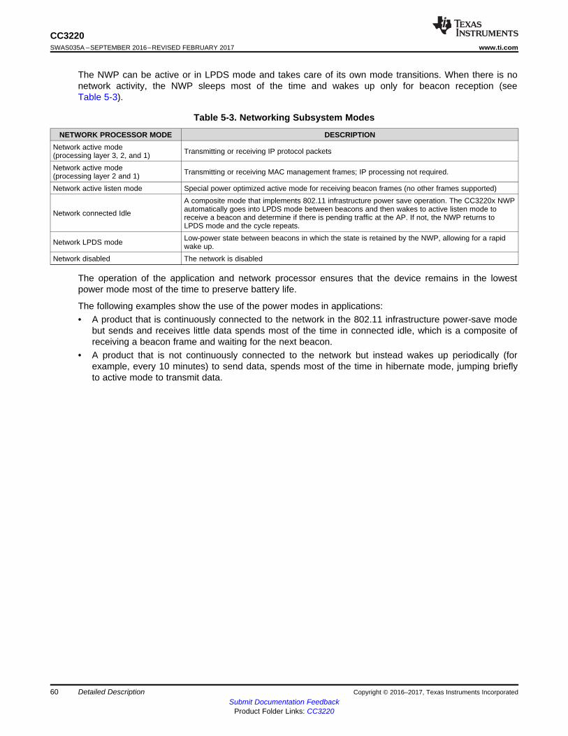
60
CC3220SWAS035A –SEPTEMBER 2016–REVISED FEBRUARY 2017 www.ti.com
Submit Documentation FeedbackProduct Folder Links: CC3220
Detailed Description Copyright © 2016–2017, Texas Instruments Incorporated
The NWP can be active or in LPDS mode and takes care of its own mode transitions. When there is nonetwork activity, the NWP sleeps most of the time and wakes up only for beacon reception (seeTable 5-3).
Table 5-3. Networking Subsystem Modes
NETWORK PROCESSOR MODE DESCRIPTIONNetwork active mode(processing layer 3, 2, and 1) Transmitting or receiving IP protocol packets
Network active mode(processing layer 2 and 1) Transmitting or receiving MAC management frames; IP processing not required.
Network active listen mode Special power optimized active mode for receiving beacon frames (no other frames supported)
Network connected Idle
A composite mode that implements 802.11 infrastructure power save operation. The CC3220x NWPautomatically goes into LPDS mode between beacons and then wakes to active listen mode toreceive a beacon and determine if there is pending traffic at the AP. If not, the NWP returns toLPDS mode and the cycle repeats.
Network LPDS mode Low-power state between beacons in which the state is retained by the NWP, allowing for a rapidwake up.
Network disabled The network is disabled
The operation of the application and network processor ensures that the device remains in the lowestpower mode most of the time to preserve battery life.
The following examples show the use of the power modes in applications:• A product that is continuously connected to the network in the 802.11 infrastructure power-save mode
but sends and receives little data spends most of the time in connected idle, which is a composite ofreceiving a beacon frame and waiting for the next beacon.
• A product that is not continuously connected to the network but instead wakes up periodically (forexample, every 10 minutes) to send data, spends most of the time in hibernate mode, jumping brieflyto active mode to transmit data.
61
CC3220www.ti.com SWAS035A –SEPTEMBER 2016–REVISED FEBRUARY 2017
Submit Documentation FeedbackProduct Folder Links: CC3220
Detailed DescriptionCopyright © 2016–2017, Texas Instruments Incorporated
(1) Including fail-safe.(2) For maximum MCU size.
5.8 Memory
5.8.1 External Memory RequirementsThe CC3220x device maintains a proprietary file system on the sFLASH. The CC3220x file system storesthe MCU binary, service pack file, system files, configuration files, certificate files, web page files, and userfiles. By using a format command through the API, users can provide the total size allocated for the filesystem. The starting address of the file system cannot be set and is always at the beginning of thesFLASH. The applications microcontroller must access the sFLASH memory area allocated to the filesystem directly through the CC3220x file system. The applications microcontroller must not access thesFLASH memory area directly.
The file system manages the allocation of sFLASH blocks for stored files according to download order,which means that the location of a specific file is not fixed in all systems. Files are stored on sFLASHusing human-readable filenames rather than file IDs. The file system API works using plain text, and fileencryption and decryption is invisible to the user. Encrypted files can be accessed only through the filesystem.
All file types can have a maximum of 100 supported files in the file system. All files are stored in 4-KBblocks and thus use a minimum of 4KB of flash space. Fail-safe files require twice the original size anduse a minimum of 8KB. Encrypted files are counted as fail-safe in terms of space. The maximum file sizeis 1MB.
Table 5-4 lists the minimum required memory consumption under the following assumptions:• System files in use consume 64 blocks (256KB).• Vendor files are not taken into account.• MCU code is taken as the maximal possible size for the CC3220 with fail-safe enabled to account for
future updates, such as through OTA.• Gang image:
– Storage for the gang image is rounded up to 32 blocks (meaning 128-KB resolution).– Gang image size depends on the actual content size of all components. Additionally, the image
should be 128-KB aligned so unaligned memory is considered lost. Service pack, system files, andthe 128-KB aligned memory are assumed to occupy 256KB.
• All calculations consider that the restore-to-default is enabled.
Table 5-4. Recommended Flash Size
ITEM CC3220R and CC3220S [KB] CC3220SF [KB]File system allocation table 20 20System and configuration files (1) 256 256Service Pack (1) 264 264MCU Code (1) 512 2048Gang image size 256 + MCU 256 + MCUTotal 1308 + MCU 2844 + MCUMinimal flash size (2) 16MBit 32MBitRecommended flash size (2) 16MBit 32MBit
space
NOTEThe maximum supported sFLASH size is 32MB (256Mb). Please refer to Using Serial Flashon CC3120/CC3220 SimpleLink™ Wi-Fi® and Internet-of-Things Devices.
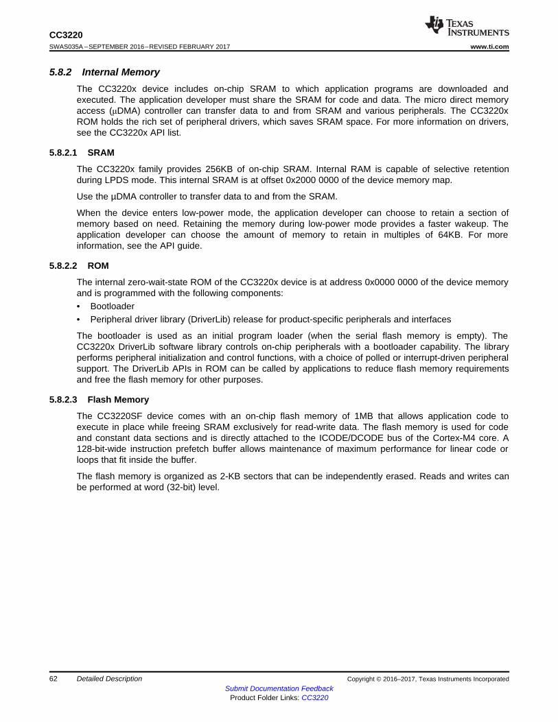
62
CC3220SWAS035A –SEPTEMBER 2016–REVISED FEBRUARY 2017 www.ti.com
Submit Documentation FeedbackProduct Folder Links: CC3220
Detailed Description Copyright © 2016–2017, Texas Instruments Incorporated
5.8.2 Internal MemoryThe CC3220x device includes on-chip SRAM to which application programs are downloaded andexecuted. The application developer must share the SRAM for code and data. The micro direct memoryaccess (μDMA) controller can transfer data to and from SRAM and various peripherals. The CC3220xROM holds the rich set of peripheral drivers, which saves SRAM space. For more information on drivers,see the CC3220x API list.
5.8.2.1 SRAM
The CC3220x family provides 256KB of on-chip SRAM. Internal RAM is capable of selective retentionduring LPDS mode. This internal SRAM is at offset 0x2000 0000 of the device memory map.
Use the µDMA controller to transfer data to and from the SRAM.
When the device enters low-power mode, the application developer can choose to retain a section ofmemory based on need. Retaining the memory during low-power mode provides a faster wakeup. Theapplication developer can choose the amount of memory to retain in multiples of 64KB. For moreinformation, see the API guide.
5.8.2.2 ROM
The internal zero-wait-state ROM of the CC3220x device is at address 0x0000 0000 of the device memoryand is programmed with the following components:• Bootloader• Peripheral driver library (DriverLib) release for product-specific peripherals and interfaces
The bootloader is used as an initial program loader (when the serial flash memory is empty). TheCC3220x DriverLib software library controls on-chip peripherals with a bootloader capability. The libraryperforms peripheral initialization and control functions, with a choice of polled or interrupt-driven peripheralsupport. The DriverLib APIs in ROM can be called by applications to reduce flash memory requirementsand free the flash memory for other purposes.
5.8.2.3 Flash Memory
The CC3220SF device comes with an on-chip flash memory of 1MB that allows application code toexecute in place while freeing SRAM exclusively for read-write data. The flash memory is used for codeand constant data sections and is directly attached to the ICODE/DCODE bus of the Cortex-M4 core. A128-bit-wide instruction prefetch buffer allows maintenance of maximum performance for linear code orloops that fit inside the buffer.
The flash memory is organized as 2-KB sectors that can be independently erased. Reads and writes canbe performed at word (32-bit) level.
63
CC3220www.ti.com SWAS035A –SEPTEMBER 2016–REVISED FEBRUARY 2017
Submit Documentation FeedbackProduct Folder Links: CC3220
Detailed DescriptionCopyright © 2016–2017, Texas Instruments Incorporated
5.8.2.4 Memory Map
Table 5-5 describes the various MCU peripherals and how they are mapped to the processor memory. Formore information on peripherals, see the API document.
Table 5-5. Memory Map
START ADDRESS END ADDRESS DESCRIPTION COMMENT0x0000 0000 0x0007 FFFF On-chip ROM (bootloader + DriverLib)0x0100 0000 0x010F FFFF On-chip flash (for user application code) CC3220FS device only0x2000 0000 0x2003 FFFF Bit-banded on-chip SRAM0x2200 0000 0x23FF FFFF Bit-band alias of 0x2000 0000 to 0x200F FFFF0x4000 0000 0x4000 0FFF Watchdog timer A00x4000 4000 0x4000 4FFF GPIO port A00x4000 5000 0x4000 5FFF GPIO port A10x4000 6000 0x4000 6FFF GPIO port A20x4000 7000 0x4000 7FFF GPIO port A30x4000 C000 0x4000 CFFF UART A00x4000 D000 0x4000 DFFF UART A10x4002 0000 0x4000 07FF I2C A0 (master)0x4002 4000 0x4002 4FFF GPIO group 40x4002 0800 0x4002 0FFF I2C A0 (slave)0x4003 0000 0x4003 0FFF General-purpose timer A00x4003 1000 0x4003 1FFF General-purpose timer A10x4003 2000 0x4003 2FFF General-purpose timer A20x4003 3000 0x4003 3FFF General-purpose timer A30x400F7000 0x400F 7FFF Configuration registers0x400F E000 0x400F EFFF System control0x400F F000 0x400F FFFF µDMA0x4200 0000 0x43FF FFFF Bit band alias of 0x4000 0000 to 0x400F FFFF0x4401 0000 0x4401 0FFF SDIO master0x4401 8000 0x4401 8FFF Camera Interface0x4401 C000 0x4401 EFFF McASP0x4402 0000 0x4402 0FFF SSPI Used for external serial flash0x4402 1000 0x4402 2FFF GSPI Used by application processor0x4402 5000 0x4402 5FFF MCU reset clock manager0x4402 6000 0x4402 6FFF MCU configuration space0x4402 D000 0x4402 DFFF Global power, reset, and clock manager (GPRCM)0x4402 E000 0x4402 EFFF MCU shared configuration0x4402 F000 0x4402 FFFF Hibernate configuration
0x4403 0000 0x4403 FFFF Crypto range (includes apertures for all crypto-relatedblocks as follows)
0x4403 0000 0x4403 0FFF DTHE registers and TCP checksum0x4403 5000 0x4403 5FFF MD5/SHA0x4403 7000 0x4403 7FFF AES0x4403 9000 0x4403 9FFF DES0xE000 0000 0xE000 0FFF Instrumentation trace Macrocell™0xE000 1000 0xE000 1FFF Data watchpoint and trace (DWT)0xE000 2000 0xE000 2FFF Flash patch and breakpoint (FPB)0xE000 E000 0xE000 EFFF NVIC0xE004 0000 0xE004 0FFF Trace port interface unit (TPIU)
64
CC3220SWAS035A –SEPTEMBER 2016–REVISED FEBRUARY 2017 www.ti.com
Submit Documentation FeedbackProduct Folder Links: CC3220
Detailed Description Copyright © 2016–2017, Texas Instruments Incorporated
Table 5-5. Memory Map (continued)START ADDRESS END ADDRESS DESCRIPTION COMMENT
0xE004 1000 0xE004 1FFF Reserved for embedded trace macrocell (ETM)0xE004 2000 0xE00F FFFF Reserved
5.9 Restoring Factory Default ConfigurationThe device has an internal recovery mechanism that allows rolling back the file system to its predefinedfactory image or restoring the factory default parameters of the device. The factory image is kept in aseparate sector on the sFLASH in a secure manner and cannot be accessed from the host processor. Thefollowing restore modes are supported:• None—no factory restore settings• Enable restore of factory default parameters• Enable restore of factory image and factory default parameters
The restore process is performed by calling SW APIs, or by pulling or forcing SOP[2:0] = 110 pins andtoggling the nRESET pin from low to high.
The process is fail-safe and resumes operation if a power failure occurs before the restore is finished. Therestore process typically takes about 8 seconds, depending on the attributes of the serial flash vendor.
5.10 Boot Modes
5.10.1 Boot Mode ListThe CC3220x device implements a sense-on-power (SoP) scheme to determine the device operationmode.
SoP values are sensed from the device pin during power up. This encoding determines the boot flow.Before the device is taken out of reset, the SoP values are copied to a register and used to determine thedevice operation mode while powering up. These values determine the boot flow as well as the defaultmapping for some of the pins (JTAG, SWD, UART0). Table 5-6 lists the pull configurations.
Table 5-6. CC3220x Functional Configurations
NAME SOP[2] SOP[1] SOP[0] SoP MODE COMMENT
UARTLOAD Pullup Pulldown Pulldown LDfrUART
Factory, lab flash, and SRAM loadsthrough the UART. The device waitsindefinitely for the UART to load code.The SOP bits then must be toggled toconfigure the device in functional mode.Also puts JTAG in 4-wire mode.
FUNCTIONAL_2WJ Pulldown Pulldown Pullup Fn2WJ
Functional development mode. In thismode, 2-pin SWD is available to thedeveloper. TMS and TCK are availablefor debugger connection.
FUNCTIONAL_4WJ Pulldown Pulldown Pulldown Fn4WJ
Functional development mode. In thismode, 4-pin JTAG is available to thedeveloper. TDI, TMS, TCK, and TDO areavailable for debugger connection.
UARTLOAD_FUNCTIONAL_4WJ Pulldown Pullup Pulldown LDfrUART_Fn4WJ
Supports flash and SRAM load throughUART and functional mode. The MCUbootloader tries to detect a UART breakon UART receive line. If the break signalis present, the device enters theUARTLOAD mode, otherwise, the deviceenters the functional mode. TDI, TMS,TCK, and TDO are available fordebugger connection.
65
CC3220www.ti.com SWAS035A –SEPTEMBER 2016–REVISED FEBRUARY 2017
Submit Documentation FeedbackProduct Folder Links: CC3220
Detailed DescriptionCopyright © 2016–2017, Texas Instruments Incorporated
Table 5-6. CC3220x Functional Configurations (continued)NAME SOP[2] SOP[1] SOP[0] SoP MODE COMMENT
RET_FACTORY_IMAGE Pulldown Pullup Pullup RetFactDefWhen device reset is toggled, the MCUbootloader kickstarts the procedure torestore factory default images.
The recommended values of pull resistors are 100 kΩ for SOP0 and SOP1 and 2.7 kΩ for SOP2. Theapplication can use SOP2 for other functions after chip has powered up. However, to avoid spurious SOPvalues from being sensed at power up, TI strongly recommends using the SOP2 pin only for outputsignals. The SOP0 and SOP1 pins are multiplexed with the WLAN analog test pins and are not availablefor other functions.
66
CC3220SWAS035A –SEPTEMBER 2016–REVISED FEBRUARY 2017 www.ti.com
Submit Documentation FeedbackProduct Folder Links: CC3220
Applications, Implementation, and Layout Copyright © 2016–2017, Texas Instruments Incorporated
6 Applications, Implementation, and Layout
NOTEInformation in the following Applications section is not part of the TI component specification,and TI does not warrant its accuracy or completeness. TI's customers are responsible fordetermining suitability of components for their purposes. Customers should validate and testtheir design implementation to confirm system functionality.
6.1 Application Information
6.1.1 Typical Application—CC3220x Wide-Voltage Mode
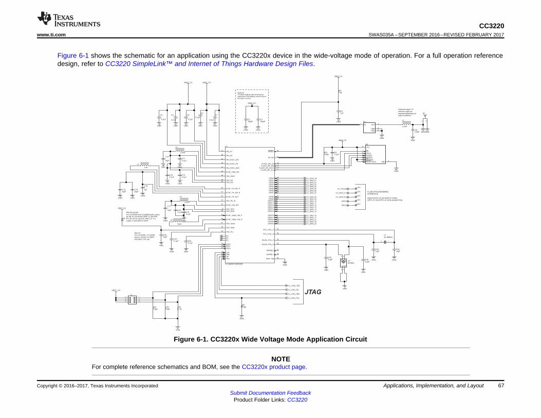
GND GND
GND
GND
GND
GNDGND
GND
GND
GNDGNDGNDGNDGND
GND
GND GND
GND
GNDGNDGND
GND GND
GND
GND GND
VBAT_CC
VBAT_CC
VBAT_CC
GND
10μFC20
10μF
C17
10μF
C10
100kR5
100kR4
100kR2
0.1μFC190.1μF
C18
0.1μF
C3
0.1μF
C7
0.1μFC21
0.1μFC22
0.1μFC11
0.1μFC8
0.1μFC12
0.1μFC13
4.7μF
C6
4.7μF
C5
4.7μF
C4
22μFC14
22μFC15
6.2pFC25
6.2pFC26
IN1
GND2
OUT3
GND4
FL1
10uH
L5
2.2uH
L4
2.2uH
L2
10pFC24
10pFC23
1uH
L3
VBAT_CCVBAT_CC
100kR3
GND
134 2
GG
40 MHzY2
0R8
12
32.768kHzY1
1 FμC2
CC_GPIO_00
CC_GPIO_01
CC_GPIO_02
CC_GPIO_03CC_GPIO_04
CC_GPIO_05
CC_GPIO_06
CC_GPIO_07
CC_GPIO_08
CC_GPIO_09
CC_GPIO_10
CC_GPIO_11CC_GPIO_12
CC_GPIO_13
CC_GPIO_16
CC_GPIO_17
CC_GPIO_22
CC_GPIO_28CC_GPIO_30
CC_GPIO_14
CC_GPIO_15
CC_JTAG_TDO
CC_JTAG_TDI
CC_JTAG_TMS
CC_JTAG_TCK
1 Fμ
C16
10kR1
2.7kR6
GPIO112
GPIO2818
VDD_PA_IN33
DCDC_PA_OUT42
GPIO050
GPIO459
GPIO134
FLASH_SPI_DOUT12
GPIO6 61
GPIO156
FLASH_SPI_CS14
WLAN_XTAL_N22
ANTSEL230
DCDC_ANA2_SW_N46
GPIO863
GPIO178
VDD_PLL24
RESET32
VDD_ANA148
VDD_DIG256
GPIO101
VDD_DIG19
LDO_IN225
DCDC_PA_SW_N41
VDD_RAM49
GPIO257
GPIO123
FLASH_SPI_CLK11
LDO_IN136
DCDC_DIG_SW43
GPIO560
GPIO14 5
FLASH_SPI_DIN13
ANTSEL1 29
DCDC_ANA_SW38
DCDC_ANA2_SW_P45
GPIO3053
GPIO762
GPIO167
GPIO2215
WLAN_XTAL_P23
RF_BG31
DCDC_PA_SW_P40
VDD_ANA247
GPIO155
GPIO964
GPIO358
GND_TAB65
SOP035
SOP134
SOP221
TMS20
TDI16
TDO17
TCK19
NC26
NC28
NC27
VIN_IO110
VIN_DCDC_DIG44
VIN_DCDC_ANA37
VIN_IO254
VIN_DCDC_PA39
RTC_XTAL_N52
RTC_XTAL_P51
U1
CC3220SF12ARGKR
GND
CS1
SO/SIO12
WP/SIO23
GND4
SI/SIO05
SCLK6
RESET/SIO37
VCC8
U2
JTAG
PIN 45 and 46:For CC3220S and CC3220R parts, leavepin 46 un-connected (DNP L5 and R8).Pin 45 can be used as GPIO_31 if asupply is provided on pin47
PIN 47:For CC3220S, CC3220Rdevice connect to VBATand add 0.1uF cap
GND
GNDGND
1 2
E1
L1
3.3nH
0.5pFC9
Antenna match. Pinetwork might berequired depending ontype of antenna.
VBAT_CC
12
3456
J1
CC_nReset
CC_GPIO_01
CC_GPIO_02
SOP0
SOP2
TP1
TP1
TP1
TP1
TP1
FLASH PROGRAMMINGINTERFACE
Add provision on the board to isolateGPIO_01 and GPIO_02 while programming
GND GND
VBAT_CC
100μFC2
100μFC3
Optional:Consider adding extra decouplingcapacitors if the battery cannot sourcethe peak currents.
Copyright © 2016–2017, Texas Instruments Incorporated Applications, Implementation, and LayoutSubmit Documentation Feedback
Product Folder Links: CC3220
67
CC3220www.ti.com SWAS035A –SEPTEMBER 2016–REVISED FEBRUARY 2017
Figure 6-1 shows the schematic for an application using the CC3220x device in the wide-voltage mode of operation. For a full operation referencedesign, refer to CC3220 SimpleLink™ and Internet of Things Hardware Design Files.
Figure 6-1. CC3220x Wide Voltage Mode Application Circuit
NOTEFor complete reference schematics and BOM, see the CC3220x product page.
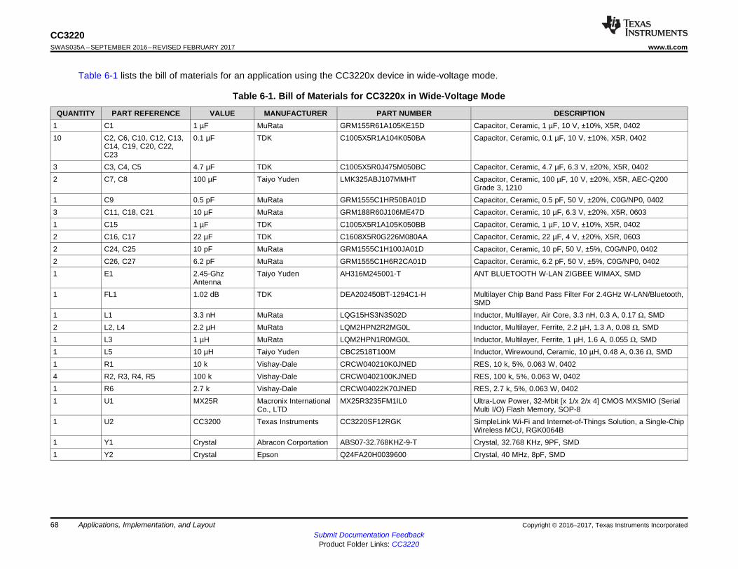
Copyright © 2016–2017, Texas Instruments IncorporatedApplications, Implementation, and LayoutSubmit Documentation Feedback
Product Folder Links: CC3220
68
CC3220SWAS035A –SEPTEMBER 2016–REVISED FEBRUARY 2017 www.ti.com
Table 6-1 lists the bill of materials for an application using the CC3220x device in wide-voltage mode.
Table 6-1. Bill of Materials for CC3220x in Wide-Voltage Mode
QUANTITY PART REFERENCE VALUE MANUFACTURER PART NUMBER DESCRIPTION1 C1 1 µF MuRata GRM155R61A105KE15D Capacitor, Ceramic, 1 µF, 10 V, ±10%, X5R, 040210 C2, C6, C10, C12, C13,
C14, C19, C20, C22,C23
0.1 µF TDK C1005X5R1A104K050BA Capacitor, Ceramic, 0.1 µF, 10 V, ±10%, X5R, 0402
3 C3, C4, C5 4.7 µF TDK C1005X5R0J475M050BC Capacitor, Ceramic, 4.7 µF, 6.3 V, ±20%, X5R, 04022 C7, C8 100 µF Taiyo Yuden LMK325ABJ107MMHT Capacitor, Ceramic, 100 µF, 10 V, ±20%, X5R, AEC-Q200
Grade 3, 12101 C9 0.5 pF MuRata GRM1555C1HR50BA01D Capacitor, Ceramic, 0.5 pF, 50 V, ±20%, C0G/NP0, 04023 C11, C18, C21 10 µF MuRata GRM188R60J106ME47D Capacitor, Ceramic, 10 µF, 6.3 V, ±20%, X5R, 06031 C15 1 µF TDK C1005X5R1A105K050BB Capacitor, Ceramic, 1 µF, 10 V, ±10%, X5R, 04022 C16, C17 22 µF TDK C1608X5R0G226M080AA Capacitor, Ceramic, 22 µF, 4 V, ±20%, X5R, 06032 C24, C25 10 pF MuRata GRM1555C1H100JA01D Capacitor, Ceramic, 10 pF, 50 V, ±5%, C0G/NP0, 04022 C26, C27 6.2 pF MuRata GRM1555C1H6R2CA01D Capacitor, Ceramic, 6.2 pF, 50 V, ±5%, C0G/NP0, 04021 E1 2.45-Ghz
AntennaTaiyo Yuden AH316M245001-T ANT BLUETOOTH W-LAN ZIGBEE WIMAX, SMD
1 FL1 1.02 dB TDK DEA202450BT-1294C1-H Multilayer Chip Band Pass Filter For 2.4GHz W-LAN/Bluetooth,SMD
1 L1 3.3 nH MuRata LQG15HS3N3S02D Inductor, Multilayer, Air Core, 3.3 nH, 0.3 A, 0.17 Ω, SMD2 L2, L4 2.2 µH MuRata LQM2HPN2R2MG0L Inductor, Multilayer, Ferrite, 2.2 µH, 1.3 A, 0.08 Ω, SMD1 L3 1 µH MuRata LQM2HPN1R0MG0L Inductor, Multilayer, Ferrite, 1 µH, 1.6 A, 0.055 Ω, SMD1 L5 10 µH Taiyo Yuden CBC2518T100M Inductor, Wirewound, Ceramic, 10 µH, 0.48 A, 0.36 Ω, SMD1 R1 10 k Vishay-Dale CRCW040210K0JNED RES, 10 k, 5%, 0.063 W, 04024 R2, R3, R4, R5 100 k Vishay-Dale CRCW0402100KJNED RES, 100 k, 5%, 0.063 W, 04021 R6 2.7 k Vishay-Dale CRCW04022K70JNED RES, 2.7 k, 5%, 0.063 W, 04021 U1 MX25R Macronix International
Co., LTDMX25R3235FM1IL0 Ultra-Low Power, 32-Mbit [x 1/x 2/x 4] CMOS MXSMIO (Serial
Multi I/O) Flash Memory, SOP-81 U2 CC3200 Texas Instruments CC3220SF12RGK SimpleLink Wi-Fi and Internet-of-Things Solution, a Single-Chip
Wireless MCU, RGK0064B1 Y1 Crystal Abracon Corportation ABS07-32.768KHZ-9-T Crystal, 32.768 KHz, 9PF, SMD1 Y2 Crystal Epson Q24FA20H0039600 Crystal, 40 MHz, 8pF, SMD
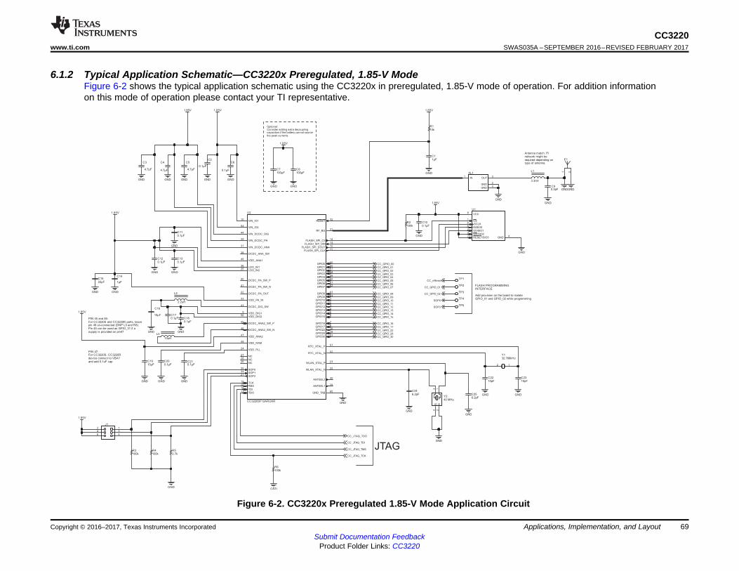
GND GND
GND
GND
GND
GNDGND
GND
GND
GNDGNDGNDGNDGND
GND GND
GND
GNDGND
GND GND
GND GND GND
1.85V
1.85V
1.85V
GND
10μFC19
10μF
C16
100kR4
100kR3
100kR2
0.1μFC180.1μF
C17
0.1μF
C2
0.1μF
C6
0.1μFC20
0.1μFC21
0.1μFC11
0.1μFC10
0.1μFC12
0.1μFC13
4.7μF
C5
4.7μF
C4
4.7μF
C3
22μFC15
6.2pFC24
6.2pFC25
IN1
GND2
OUT3
GND4
FL1
10uH
L3
2.2uH
L2
10pFC23
10pFC22
1.85V1.85V
100kR6
GND
134 2
GG
40 MHzY2
12
32.768kHzY1
1 FμC1
CC_GPIO_00
CC_GPIO_01
CC_GPIO_02
CC_GPIO_03CC_GPIO_04
CC_GPIO_05
CC_GPIO_06
CC_GPIO_07
CC_GPIO_08
CC_GPIO_09
CC_GPIO_10
CC_GPIO_11CC_GPIO_12
CC_GPIO_13
CC_GPIO_16
CC_GPIO_17
CC_GPIO_22
CC_GPIO_28CC_GPIO_30
CC_GPIO_14
CC_GPIO_15
CC_JTAG_TDO
CC_JTAG_TDI
CC_JTAG_TMS
CC_JTAG_TCK
1 Fμ
C14
10kR1
2.7kR5
GPIO112
GPIO2818
VDD_PA_IN33
DCDC_PA_OUT42
GPIO050
GPIO459
GPIO134
FLASH_SPI_DOUT12
GPIO6 61
GPIO156
FLASH_SPI_CS14
WLAN_XTAL_N22
ANTSEL230
DCDC_ANA2_SW_N46
GPIO863
GPIO178
VDD_PLL24
RESET32
VDD_ANA148
VDD_DIG256
GPIO101
VDD_DIG19
LDO_IN225
DCDC_PA_SW_N41
VDD_RAM49
GPIO257
GPIO123
FLASH_SPI_CLK11
LDO_IN136
DCDC_DIG_SW43
GPIO560
GPIO14 5
FLASH_SPI_DIN13
ANTSEL1 29
DCDC_ANA_SW38
DCDC_ANA2_SW_P45
GPIO3053
GPIO762
GPIO167
GPIO2215
WLAN_XTAL_P23
RF_BG31
DCDC_PA_SW_P40
VDD_ANA247
GPIO155
GPIO964
GPIO358
GND_TAB65
SOP035
SOP134
SOP221
TMS20
TDI16
TDO17
TCK19
NC26
NC28
NC27
VIN_IO110
VIN_DCDC_DIG44
VIN_DCDC_ANA37
VIN_IO254
VIN_DCDC_PA39
RTC_XTAL_N52
RTC_XTAL_P51
U2
CC3220SF12ARGKR
GND
CS1
SO/SIO12
WP/SIO23
GND4
SI/SIO05
SCLK6
RESET/SIO37
VCC8
U1
JTAG
PIN 45 and 46:For CC3220S and CC3220R parts, leavepin 46 un-connected (DNP L5 and R8).Pin 45 can be used as GPIO_31 if asupply is provided on pin47
PIN 47:For CC3220S, CC3220Rdevice connect to VBATand add 0.1uF cap
GND
GNDGND
1 2
E1
L1
3.3nH
0.5pFC9
Antenna match. Pinetwork might berequired depending ontype of antenna.
1.85V
1234
56
J1
CC_nReset
CC_GPIO_01
CC_GPIO_02
SOP0
SOP2
TP1
TP2
TP3
TP4
TP5
FLASH PROGRAMMINGINTERFACE
Add provision on the board to isolateGPIO_01 and GPIO_02 while programming
GND GND
1.85V
100μFC7
100μFC8
Optional:Consider adding extra decouplingcapacitors if the battery cannot sourcethe peak currents.
1.85V
Copyright © 2016–2017, Texas Instruments Incorporated Applications, Implementation, and LayoutSubmit Documentation Feedback
Product Folder Links: CC3220
69
CC3220www.ti.com SWAS035A –SEPTEMBER 2016–REVISED FEBRUARY 2017
6.1.2 Typical Application Schematic—CC3220x Preregulated, 1.85-V ModeFigure 6-2 shows the typical application schematic using the CC3220x in preregulated, 1.85-V mode of operation. For addition informationon this mode of operation please contact your TI representative.
Figure 6-2. CC3220x Preregulated 1.85-V Mode Application Circuit
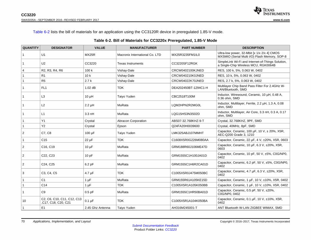
Copyright © 2016–2017, Texas Instruments IncorporatedApplications, Implementation, and LayoutSubmit Documentation Feedback
Product Folder Links: CC3220
70
CC3220SWAS035A –SEPTEMBER 2016–REVISED FEBRUARY 2017 www.ti.com
Table 6-2 lists the bill of materials for an application using the CC3120R device in preregulated 1.85-V mode.
Table 6-2. Bill of Materials for CC3220x Preregulated, 1.85-V Mode
QUANTITY DESIGNATOR VALUE MANUFACTURER PART NUMBER DESCRIPTION
1 U1 MX25R Macronix International Co. LTD MX25R3235FM1IL0 Ultra-low power, 32-Mbit [x 1/x 2/x 4] CMOSMXSMIO (Serial Multi I/O) Flash Memory, SOP-8
1 U2 CC3220 Texas Instruments CC3220SF12RGK SimpleLink Wi-Fi and Internet-of-Things Solution,a Single-Chip Wireless MCU, RGK0064B
4 R2, R3, R4, R6 100 k Vishay-Dale CRCW0402100KJNED RES, 100 k, 5%, 0.063 W, 04021 R1 10 k Vishay-Dale CRCW040210K0JNED RES, 10 k, 5%, 0.063 W, 04021 R5 2.7 k Vishay-Dale CRCW04022K70JNED RES, 2.7 k, 5%, 0.063 W, 0402
1 FL1 1.02 dB TDK DEA202450BT-1294C1-H Multilayer Chip Band Pass Filter For 2.4GHz W-LAN/Bluetooth, SMD
1 L3 10 µH Taiyo Yuden CBC2518T100M Inductor, Wirewound, Ceramic, 10 µH, 0.48 A,0.36 ohm, SMD
1 L2 2.2 µH MuRata LQM2HPN2R2MG0L Inductor, Multilayer, Ferrite, 2.2 µH, 1.3 A, 0.08ohm, SMD
1 L1 3.3 nH MuRata LQG15HS3N3S02D Inductor, Multilayer, Air Core, 3.3 nH, 0.3 A, 0.17ohm, SMD
1 Y1 Crystal Abracon Corporation ABS07-32.768KHZ-9-T Crystal, 32.768KHZ, 9PF, SMD1 Y2 Crystal Epson Q24FA20H0039600 Crystal, 40MHz, 8pF, SMD
2 C7, C8 100 µF Taiyo Yuden LMK325ABJ107MMHT Capacitor, Ceramic, 100 µF, 10 V, ± 20%, X5R,AEC-Q200 Grade 3, 1210
1 C15 22 µF TDK C1608X5R0G226M080AA Capacitor, Ceramic, 22 µF, 4 V, ±20%, X5R, 0603
2 C16, C19 10 µF MuRata GRM188R60J106ME47D Capacitor, Ceramic, 10 µF, 6.3 V, ±20%, X5R,0603
2 C22, C23 10 pF MuRata GRM1555C1H100JA01D Capacitor, Ceramic, 10 pF, 50 V, ±5%, C0G/NP0,0402
2 C24, C25 6.2 pF MuRata GRM1555C1H6R2CA01D Capacitor, Ceramic, 6.2 pF, 50 V, ±5%, C0G/NP0,0402
3 C3, C4, C5 4.7 µF TDK C1005X5R0J475M050BC Capacitor, Ceramic, 4.7 µF, 6.3 V, ±20%, X5R,0402
1 C1 1 µF MuRata GRM155R61A105KE15D Capacitor, Ceramic, 1 µF, 10 V, ±10%, X5R, 04021 C14 1 µF TDK C1005X5R1A105K050BB Capacitor, Ceramic, 1 µF, 10 V, ±10%, X5R, 0402
1 C9 0.5 pF MuRata GRM1555C1HR50BA01D Capacitor, Ceramic, 0.5 pF, 50 V, ±20%,C0G/NP0, 0402
10 C2, C6, C10, C11, C12, C13,C17, C18, C20, C21 0.1 µF TDK C1005X5R1A104K050BA Capacitor, Ceramic, 0.1 µF, 10 V, ±10%, X5R,
04021 E1 2.45 Ghz Antenna Taiyo Yuden AH316M245001-T ANT Bluetooth W-LAN ZIGBEE WIMAX, SMD
71
CC3220www.ti.com SWAS035A –SEPTEMBER 2016–REVISED FEBRUARY 2017
Submit Documentation FeedbackProduct Folder Links: CC3220
Applications, Implementation, and LayoutCopyright © 2016–2017, Texas Instruments Incorporated
6.2 PCB Layout GuidelinesThis section details the PCB guidelines to speed up the PCB design using the CC3220x VQFN device.Follow these guidelines ensures that the design will minimize the risk with regulatory certificationsincluding FCC, ETSI, and CE. For more information, see CC3120 and CC3220 SimpleLink™ Wi-Fi® andIoT Solution Layout Guidelines.
6.2.1 General PCB GuidelinesUse the following PCB guidelines:• Verify the recommended PCB stackup in the PCB design guidelines, as well as the recommended
layers for signals and ground.• Ensure that the QFN PCB footprint follows the information in Section 8.• Ensure that the QFN PCB GND and solder paste follow the recommendations provided in CC3120 and
CC3220 SimpleLink™ Wi-Fi® and IoT Solution Layout Guidelines.• Decoupling capacitors must be as close as possible to the QFN device.
6.2.2 Power Layout and RoutingThree critical DC-DC converters must be considered for the CC3220x device.• Analog DC-DC converter• PA DC-DC converter• Digital DC-DC converter
Each converter requires an external inductor and capacitor that must be laid out with care. DC currentloops are formed when laying out the power components.
6.2.2.1 Design Considerations
The following design guidelines must be followed when laying out the CC3220x device:• Route all of the input decoupling capacitors (C11, C13, and C18) on L2 using thick traces, to isolate
the RF ground from the noisy supply ground. This step is also required to meet the IEEE spectral maskspecifications.
• Maintain the thickness of power traces to be greater than 12 mils. Take special consideration for poweramplifier supply lines (pin 33, 40, 41, and 42), and all input supply pins (pin 37, 39, and 44).
• Ensure the shortest grounding loop for the PLL supply decoupling capacitor (pin 24).• Place all decoupling capacitors as close to the respective pins as possible.• Power budget: The CC3220x device can consume up to 450 mA for 3.3 V, 670 mA for 2.1 V, and 700
mA for 1.85 V, for 24 ms during the calibration cycle.• Ensure the power supply is designed to source this current without any issues. The complete
calibration (TX and RX) can take up to 17 mJ of energy from the battery over a time of 24 ms.• The CC3220x device contains many high-current input pins. Ensure the trace feeding these pins is
capable of handling the following currents:– PA DCDC input (pin 39) maximum 1 A– ANA DCDC input (pin 37) maximum 600 mA– DIG DCDC input (pin 44) maximum 500 mA– PA DCDC switching nodes (pin 40 and pin 41) maximum 1 A– PA DCDC output node (pin 42) maximum 1 A– ANA DCDC switching node (pin 38) maximum 600 mA– DIG DCDC switching node (pin 43) maximum 500 mA– PA supply (pin 33) maximum 500 mA
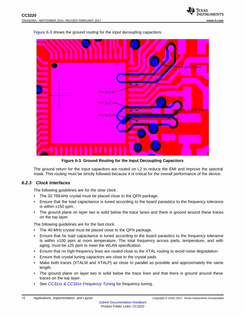
72
CC3220SWAS035A –SEPTEMBER 2016–REVISED FEBRUARY 2017 www.ti.com
Submit Documentation FeedbackProduct Folder Links: CC3220
Applications, Implementation, and Layout Copyright © 2016–2017, Texas Instruments Incorporated
Figure 6-3 shows the ground routing for the input decoupling capacitors.
Figure 6-3. Ground Routing for the Input Decoupling Capacitors
The ground return for the input capacitors are routed on L2 to reduce the EMI and improve the spectralmask. This routing must be strictly followed because it is critical for the overall performance of the device.
6.2.3 Clock InterfacesThe following guidelines are for the slow clock.• The 32.768-kHz crystal must be placed close to the QFN package.• Ensure that the load capacitance is tuned according to the board parasitics to the frequency tolerance
is within ±150 ppm.• The ground plane on layer two is solid below the trace lanes and there is ground around these traces
on the top layer.
The following guidelines are for the fast clock.• The 40-MHz crystal must be placed close to the QFN package.• Ensure that he load capacitance is tuned according to the board parasitics to the frequency tolerance
is within ±100 ppm at room temperature. The total frequency across parts, temperature, and withaging, must be ±25 ppm to meet the WLAN specification.
• Ensure that no high-frequency lines are routed close to the XTAL routing to avoid noise degradation.• Ensure that crystal tuning capacitors are close to the crystal pads.• Make both traces (XTALM and XTALP) as close to parallel as possible and approximately the same
length.• The ground plane on layer two is solid below the trace lines and that there is ground around these
traces on the top layer.• See CC31xx & CC32xx Frequency Tuning for frequency tuning.
73
CC3220www.ti.com SWAS035A –SEPTEMBER 2016–REVISED FEBRUARY 2017
Submit Documentation FeedbackProduct Folder Links: CC3220
Applications, Implementation, and LayoutCopyright © 2016–2017, Texas Instruments Incorporated
6.2.4 Digital Input and OutputThe following guidelines are for the digital I/O.• Route SPI and UART lines away from any RF traces.• Keep the length of the high-speed lines as short as possible to avoid transmission line effects.• Keep the line lower than 1/10 of the rise time of the signal to ignore transmission line effects. This is
required if the traces cannot be kept short. Place the resistor at the source end, closer to the devicethat is driving the signal.
• Add series-terminating resistor for each high-speed line (such as SPI_CLK or SPI_DATA) to match thedriver impedance to the line. Typical terminating-resistor values range from 27 to 36 Ω for a 50-Ω lineimpedance.
• Route high-speed lines with a ground reference plane continuously below it to offer good impedancethroughout. This routing also helps shield the trace against EMI.
• Avoid stubs on high-speed lines to minimize the reflections. If the line must be routed to multiplelocations, use a separate line driver for each line.
• If the lines are longer compared to the rise time, add series-terminating resistors near the driver foreach high-speed line to match the driver impedance to the line. Typical terminating-resistor valuesrange from 27 to 36 Ω for a 50-Ω line impedance.
6.2.5 RF InterfaceThe following guidelines are for the RF interface. Follow guidelines specified in the vendor-specificantenna design guides (including placement of the antenna). Also see CC3120 and CC3220 SimpleLink™Wi-Fi® and IoT Solution Layout Guidelines for general antenna guidelines.• Ensure that the antenna is matched for 50-Ω. A Pi-matching network is recommended.• Ensure that the area underneath the BPF pads are grounded on layer one and layer two, and that the
minimum fulter requirements are met.• Verify that the Wi-Fi RF trace is a 50-Ω, impedance-controlled trace with a reference to solid ground.• The RF trace bends must be made with gradual curves, and 90-degree bends must be avoided.• The RF traces must not have sharp corners.• There must be no traces or ground under the antenna section.• The RF traces must have via stitching on the ground plane beside the RF trace on both sides.
74
CC3220SWAS035A –SEPTEMBER 2016–REVISED FEBRUARY 2017 www.ti.com
Submit Documentation FeedbackProduct Folder Links: CC3220
Device and Documentation Support Copyright © 2016–2017, Texas Instruments Incorporated
7 Device and Documentation Support
TI offers an extensive line of development tools. Tools and software to evaluate the performance of thedevice, generate code, and develop solutions are listed in this section.
7.1 Tools and SoftwareDevelopment ToolsPin Mux Tool The supported devices are: CC3200 and CC3220x.
The Pin Mux Tool is a software tool that provides a graphical user interface (GUI) forconfiguring pin multiplexing settings, resolving conflicts and specifying I/O cell characteristicsfor MPUs from TI. Results are output as C header/code files that can be imported intosoftware development kits (SDKs) or used to configure customers' custom software. Version3 of the Pin Mux Tool adds the capability of automatically selecting a mux configuration thatsatisfies the entered requirements.
SimpleLink Wi-Fi Radio Testing Tool The supported devices are: CC3100, CC3200, and CC3220x.The SimpleLink™ Wi-Fi® Radio Testing Tool is a Windows-based software tool for RFevaluation and testing of SimpleLink Wi-Fi CC31xx and CC32xx designs during developmentand certification. The tool enables low-level radio testing capabilities by manually setting theradio into transmit or receive modes. Using the tool requires familiarity and knowledge ofradio circuit theory and radio test methods.Created for the Internet of Things (IoT), the SimpleLink Wi-Fi CC31xx and CC32xx family ofdevices include on-chip Wi-Fi, Internet, and robust security protocols with no prior Wi-Fiexperience needed for faster development. For more information on these devices, visitSimpleLink™ Wi-Fi® family, Internet-on-a-chip™ solutions.
SimpleLink Wi-Fi Starter Pro The supported devices are: CC3100, CC3200, CC3120R, and CC3220x.The SimpleLink™ Wi-Fi® Starter Pro mobile App is a new mobile application for SimpleLinkprovisioning. The app goes along with the embedded provisioning library and example thatruns on the device side (can be found under SDKs CC3120RSDK and CC3220SDK). Thenew provisioning release is a TI recommendation for Wi-Fi provisioning using SimpleLink Wi-Fi products. The provisioning release implements advanced AP mode and SmartConfig™technology provisioning with feedback and fallback options to ensure successful process hasbeen accomplished. Customers can use both embedded library and the mobile library forintegration to their end products.
Image Creator The supported devices are: CC3120R and CC3220x.Image Creator is a web application which is used to create a programming image; it can alsowrite the programming image into the SimpleLink CC3x20 devices. The programming imageis a file which contains the SimpleLink device configurations and files required for theoperation of the device. For the SimpleLink CC3220 wireless microcontroller, the ImageCreator can also include the host application file. A new SimpleLink device should first beprogrammed by a programming image. The image, created by the Image Creator, can beprogrammed onto the device as part of the production procedure or when in developmentstage.
CC3220 Software Development Kit (SDK) The CC3220x device is supported.The CC3220 SDK contains drivers, many sample applications for Wi-Fi features andInternet, as well as documentation needed to use the CC3220 Internet-on-a-chip solution.This SDK can be used with TI’s MSP432P401R LaunchPad™ development kit, or with theSimpleLink Studio, a PC tool that allows MCU development with CC3220. You can also usethe SDK as example code for any platform. All sample applications in the SDK are supportedon TI’s MSP432P401R ultra-low-power MCUs with Code Composer Studio™ IDE and TI-RTOS. In addition, many of the applications support IAR.
TI Designs and Reference Designs
The TI Designs Reference Design Library is a robust reference design library spanning analog, embeddedprocessor, and connectivity. Created by TI experts to help you jumpstart your system design, all TIDesigns include schematic or block diagrams, BOMs, and design files to speed your time to market.
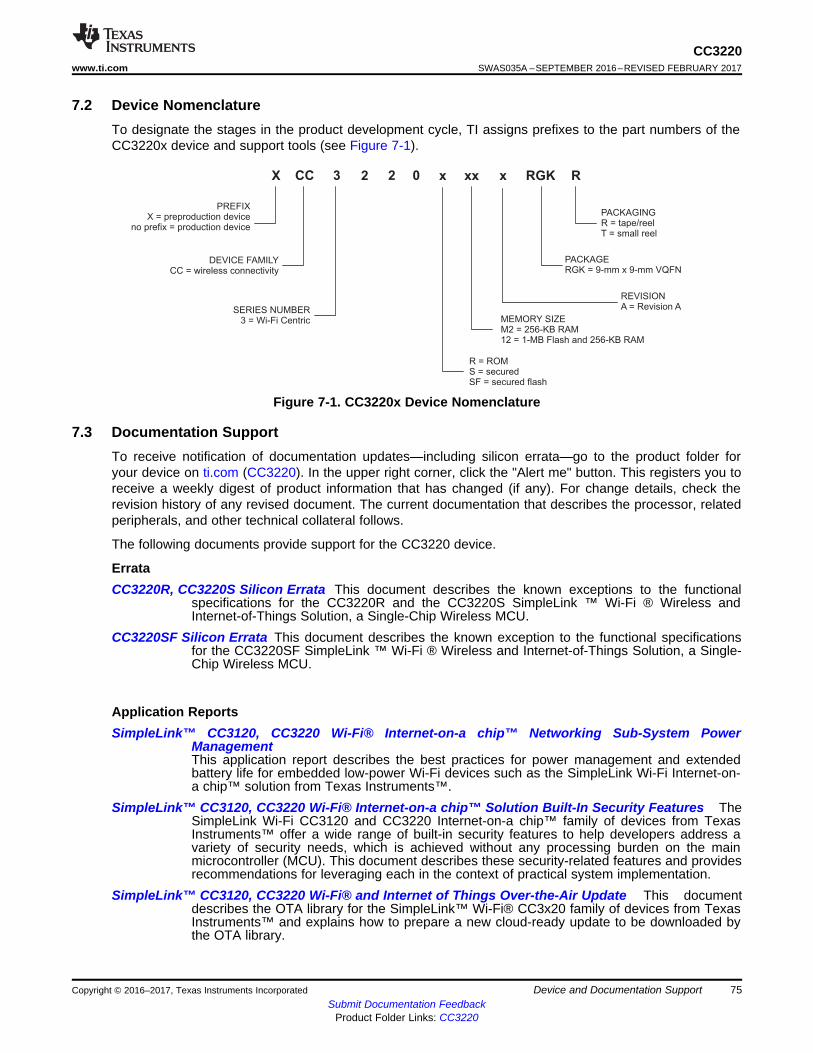
X
PREFIXX = preproduction device
no prefix = production device
CC 3 2 2 0 x xx RGK R
DEVICE FAMILYCC = wireless connectivity
SERIES NUMBER3 = Wi-Fi Centric MEMORY SIZE
M2 = 256-KB RAM12 = 1-MB Flash and 256-KB RAM
PACKAGERGK = 9-mm x 9-mm VQFN
PACKAGINGR = tape/reelT = small reel
R = ROMS = securedSF = secured flash
x
REVISIONA = Revision A
75
CC3220www.ti.com SWAS035A –SEPTEMBER 2016–REVISED FEBRUARY 2017
Submit Documentation FeedbackProduct Folder Links: CC3220
Device and Documentation SupportCopyright © 2016–2017, Texas Instruments Incorporated
7.2 Device NomenclatureTo designate the stages in the product development cycle, TI assigns prefixes to the part numbers of theCC3220x device and support tools (see Figure 7-1).
Figure 7-1. CC3220x Device Nomenclature
7.3 Documentation SupportTo receive notification of documentation updates—including silicon errata—go to the product folder foryour device on ti.com (CC3220). In the upper right corner, click the "Alert me" button. This registers you toreceive a weekly digest of product information that has changed (if any). For change details, check therevision history of any revised document. The current documentation that describes the processor, relatedperipherals, and other technical collateral follows.
The following documents provide support for the CC3220 device.
ErrataCC3220R, CC3220S Silicon Errata This document describes the known exceptions to the functional
specifications for the CC3220R and the CC3220S SimpleLink ™ Wi-Fi ® Wireless andInternet-of-Things Solution, a Single-Chip Wireless MCU.
CC3220SF Silicon Errata This document describes the known exception to the functional specificationsfor the CC3220SF SimpleLink ™ Wi-Fi ® Wireless and Internet-of-Things Solution, a Single-Chip Wireless MCU.
Application ReportsSimpleLink™ CC3120, CC3220 Wi-Fi® Internet-on-a chip™ Networking Sub-System Power
ManagementThis application report describes the best practices for power management and extendedbattery life for embedded low-power Wi-Fi devices such as the SimpleLink Wi-Fi Internet-on-a chip™ solution from Texas Instruments™.
SimpleLink™ CC3120, CC3220 Wi-Fi® Internet-on-a chip™ Solution Built-In Security Features TheSimpleLink Wi-Fi CC3120 and CC3220 Internet-on-a chip™ family of devices from TexasInstruments™ offer a wide range of built-in security features to help developers address avariety of security needs, which is achieved without any processing burden on the mainmicrocontroller (MCU). This document describes these security-related features and providesrecommendations for leveraging each in the context of practical system implementation.
SimpleLink™ CC3120, CC3220 Wi-Fi® and Internet of Things Over-the-Air Update This documentdescribes the OTA library for the SimpleLink™ Wi-Fi® CC3x20 family of devices from TexasInstruments™ and explains how to prepare a new cloud-ready update to be downloaded bythe OTA library.
76
CC3220SWAS035A –SEPTEMBER 2016–REVISED FEBRUARY 2017 www.ti.com
Submit Documentation FeedbackProduct Folder Links: CC3220
Device and Documentation Support Copyright © 2016–2017, Texas Instruments Incorporated
SimpleLink™ CC3120, CC3220 Wi-Fi® Internet-on-a chip™ Solution Device Provisioning This guidedescribes the provisioning process, which provides the SimpleLink Wi-Fi device with theinformation (network name, password, and so forth) needed to connect to a wirelessnetwork.
Using Serial Flash on SimpleLink™ CC3120 and CC3220 Wi-Fi® and Internet-of-Things DevicesThis application note is divided into two parts. The first part provides important guidelinesand best- practice design techniques to consider when choosing and embedding a serialflash paired with the CC3120 and CC3220 (CC3x20) devices. The second part describes thefile system, along with guidelines and considerations for system designers working with theCC3x20 devices.
User's GuidesSimpleLink™ Wi-Fi® and Internet of Things CC3120 and CC3220 Network Processor This document
provides software (SW) programmers with all of the required knowledge for working with thenetworking subsystem of the SimpleLink Wi-Fi devices. This guide provides basic guidelinesfor writing robust, optimized networking host applications, and describes the capabilities ofthe networking subsystem. The guide contains some example code snapshots, to give usersan idea of how to work with the host driver. More comprehensive code examples can befound in the formal software development kit (SDK). This guide does not provide a detaileddescription of the host driver APIs.
SimpleLink™ Wi-Fi® CC3120 and CC3220 and IoT Solution Layout Guidelines This documentprovides the design guidelines of the 4-layer PCB used for the CC3120 and CC3220SimpleLink Wi-Fi family of devices from Texas Instruments™. The CC3120 and CC3220devices are easy to lay out and are available in quad flat no-leads (QFNS) packages. Whendesigning the board, follow the suggestions in this document to optimize performance of theboard.
SimpleLink™ Wi-Fi® and Internet of Things Solution CC3220, a Single-Chip Wireless MCU Thisguide is intended to assist users in the initial setup and demonstration of running their firstsample application for the CC3220, CC3220S, CC3220SF SimpleLink™ Wi-Fi® and Internetof Things Solution, a Single-Chip Wireless MCU from Texas Instruments™. The guideexplains how to install the software development kit (SDK) and various other tools requiredto get started with the first application.
SimpleLink™ CC3220 Wi-Fi® LaunchPad™ Development Kit HardwareThe CC3220 SimpleLinkLaunchPad™ Development Kit (CC3220-LAUNCHXL) is a low-cost evaluation platform forARM® Cortex®-M4-based MCUs. The LaunchPad design highlights the CC3220 Internet-on-a chip™ solution and Wi-Fi capabilities. The CC3220 LaunchPad also features temperatureand accelerometer sensors, programmable user buttons, three LEDs for customapplications, and onboard emulation for debugging. The stackable headers of the CC3220LaunchPad XL interface demonstrate how easy it is to expand the functionality of theLaunchPad when interfacing with other peripherals on many existing BoosterPack™ Plug-inModule add-on boards, such as graphical displays, audio codecs, antenna selection,environmental sensing, and more.
SimpleLink™ Wi-Fi® and Internet of Things CC3220This document introduces the user to theenvironment setup for the CC3220x device, along with some reference examples from thesoftware development kit (SDK). This document explains both the platform and theframework available to enable further application development.
SimpleLink™ Wi-Fi® CC3220 Out-of-Box ApplicationThis guide demonstrates the out-of-boxexperience for the CC3220 LaunchPad™ Development Kit, highlighting the easy connectionto the CC3220 LaunchPad using the SimpleLink™ Wi-Fi® Starter Pro application, and theover-the-air update.
SimpleLink™ Wi-Fi® and Internet-on-a-chip™ CC3120 and CC3220 Solution Radio Tool The RadioTool serves as a control panel for direct access to the radio, and can be used for both theradio frequency (RF) evaluation and for certification purposes. This guide describes how tohave the tool work seamlessly on Texas Instruments ™ evaluation platforms such as theBoosterPack™ plus FTDI emulation board for CC3120 devices, and the LaunchPad™ forCC3220 devices.
SimpleLink™ Wi-Fi® CC3120 and CC3220 Provisioning for Mobile Applications This guide describesTI’s SimpleLink™ Wi-Fi® provisioning solution for mobile applications, specifically on theusage of the Android™ and iOS® building blocks for UI requirements, networking, andprovisioning APIs required for building the mobile application.
77
CC3220www.ti.com SWAS035A –SEPTEMBER 2016–REVISED FEBRUARY 2017
Submit Documentation FeedbackProduct Folder Links: CC3220
Device and Documentation SupportCopyright © 2016–2017, Texas Instruments Incorporated
SimpleLink™ Wi-Fi® CC3220 Out-of-Box ApplicationThis guide details the out-of-box (OOB)experience with the CC3220 LaunchPad™ Development Kit from Texas Instruments™.
More LiteratureCC3220, CC3220S, CC3220SF SimpleLink™ Wi-Fi ® and Internet of ThingsThis document is the
technical reference manual for the CC3220 device.RemoTI ManifestCC3220 SimpleLink™ Wi-Fi® and Internet of Things CC3220 hardware design files.
7.4 Community ResourcesThe following links connect to TI community resources. Linked contents are provided "AS IS" by therespective contributors. They do not constitute TI specifications and do not necessarily reflect TI's views;see TI's Terms of Use.TI E2E™ Online Community The TI engineer-to-engineer (E2E) community was created to foster
collaboration among engineers. At e2e.ti.com, you can ask questions, share knowledge,explore ideas and help solve problems with fellow engineers.
TI Embedded Processors Wiki Established to help developers get started with Embedded Processorsfrom Texas Instruments and to foster innovation and growth of general knowledge about thehardware and software surrounding these devices.
78
CC3220SWAS035A –SEPTEMBER 2016–REVISED FEBRUARY 2017 www.ti.com
Submit Documentation FeedbackProduct Folder Links: CC3220
Device and Documentation Support Copyright © 2016–2017, Texas Instruments Incorporated
7.5 TrademarksSimpleLink, Internet-on-a-chip, SmartConfig, Texas Instruments, E2E, LaunchPad, Code ComposerStudio are trademarks of Texas Instruments.ARM, Cortex, Thumb are registered trademarks of ARM Ltd.Bluetooth is a registered trademark of Bluetooth SIG, Inc.Macrocell is a trademark of Kappa Global Inc.Wi-Fi CERTIFIED is a trademark of Wi-Fi Alliance.Wi-Fi, Wi-Fi Direct are registered trademarks of Wi-Fi Alliance.All other trademarks are the property of their respective owners.
7.6 Electrostatic Discharge CautionThis integrated circuit can be damaged by ESD. Texas Instruments recommends that all integrated circuits be handled withappropriate precautions. Failure to observe proper handling and installation procedures can cause damage.
ESD damage can range from subtle performance degradation to complete device failure. Precision integrated circuits may be moresusceptible to damage because very small parametric changes could cause the device not to meet its published specifications.
7.7 Export Control NoticeRecipient agrees to not knowingly export or re-export, directly or indirectly, any product or technical data(as defined by the U.S., EU, and other Export Administration Regulations) including software, or anycontrolled product restricted by other applicable national regulations, received from disclosing party undernondisclosure obligations (if any), or any direct product of such technology, to any destination to whichsuch export or re-export is restricted or prohibited by U.S. or other applicable laws, without obtaining priorauthorization from U.S. Department of Commerce and other competent Government authorities to theextent required by those laws.
7.8 GlossaryTI Glossary This glossary lists and explains terms, acronyms, and definitions.
79
CC3220www.ti.com SWAS035A –SEPTEMBER 2016–REVISED FEBRUARY 2017
Submit Documentation FeedbackProduct Folder Links: CC3220
Mechanical, Packaging, and Orderable InformationCopyright © 2016–2017, Texas Instruments Incorporated
8 Mechanical, Packaging, and Orderable Information
The following pages include mechanical, packaging, and orderable information. This information is themost current data available for the designated devices. This data is subject to change without notice andrevision of this document. For browser-based versions of this data sheet, refer to the left-hand navigation.
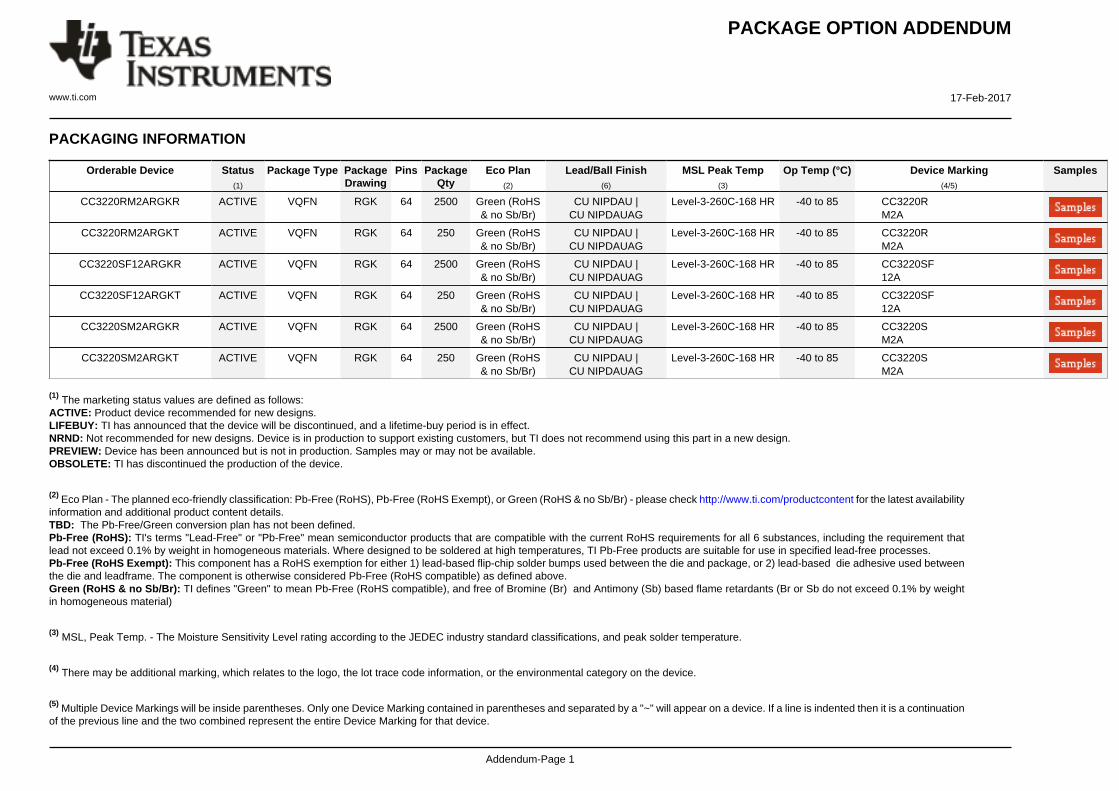
PACKAGE OPTION ADDENDUM
www.ti.com 17-Feb-2017
Addendum-Page 1
PACKAGING INFORMATION
Orderable Device Status(1)
Package Type PackageDrawing
Pins PackageQty
Eco Plan(2)
Lead/Ball Finish(6)
MSL Peak Temp(3)
Op Temp (°C) Device Marking(4/5)
Samples
CC3220RM2ARGKR ACTIVE VQFN RGK 64 2500 Green (RoHS& no Sb/Br)
CU NIPDAU |CU NIPDAUAG
Level-3-260C-168 HR -40 to 85 CC3220RM2A
CC3220RM2ARGKT ACTIVE VQFN RGK 64 250 Green (RoHS& no Sb/Br)
CU NIPDAU |CU NIPDAUAG
Level-3-260C-168 HR -40 to 85 CC3220RM2A
CC3220SF12ARGKR ACTIVE VQFN RGK 64 2500 Green (RoHS& no Sb/Br)
CU NIPDAU |CU NIPDAUAG
Level-3-260C-168 HR -40 to 85 CC3220SF12A
CC3220SF12ARGKT ACTIVE VQFN RGK 64 250 Green (RoHS& no Sb/Br)
CU NIPDAU |CU NIPDAUAG
Level-3-260C-168 HR -40 to 85 CC3220SF12A
CC3220SM2ARGKR ACTIVE VQFN RGK 64 2500 Green (RoHS& no Sb/Br)
CU NIPDAU |CU NIPDAUAG
Level-3-260C-168 HR -40 to 85 CC3220SM2A
CC3220SM2ARGKT ACTIVE VQFN RGK 64 250 Green (RoHS& no Sb/Br)
CU NIPDAU |CU NIPDAUAG
Level-3-260C-168 HR -40 to 85 CC3220SM2A
(1) The marketing status values are defined as follows:ACTIVE: Product device recommended for new designs.LIFEBUY: TI has announced that the device will be discontinued, and a lifetime-buy period is in effect.NRND: Not recommended for new designs. Device is in production to support existing customers, but TI does not recommend using this part in a new design.PREVIEW: Device has been announced but is not in production. Samples may or may not be available.OBSOLETE: TI has discontinued the production of the device.
(2) Eco Plan - The planned eco-friendly classification: Pb-Free (RoHS), Pb-Free (RoHS Exempt), or Green (RoHS & no Sb/Br) - please check http://www.ti.com/productcontent for the latest availabilityinformation and additional product content details.TBD: The Pb-Free/Green conversion plan has not been defined.Pb-Free (RoHS): TI's terms "Lead-Free" or "Pb-Free" mean semiconductor products that are compatible with the current RoHS requirements for all 6 substances, including the requirement thatlead not exceed 0.1% by weight in homogeneous materials. Where designed to be soldered at high temperatures, TI Pb-Free products are suitable for use in specified lead-free processes.Pb-Free (RoHS Exempt): This component has a RoHS exemption for either 1) lead-based flip-chip solder bumps used between the die and package, or 2) lead-based die adhesive used betweenthe die and leadframe. The component is otherwise considered Pb-Free (RoHS compatible) as defined above.Green (RoHS & no Sb/Br): TI defines "Green" to mean Pb-Free (RoHS compatible), and free of Bromine (Br) and Antimony (Sb) based flame retardants (Br or Sb do not exceed 0.1% by weightin homogeneous material)
(3) MSL, Peak Temp. - The Moisture Sensitivity Level rating according to the JEDEC industry standard classifications, and peak solder temperature.
(4) There may be additional marking, which relates to the logo, the lot trace code information, or the environmental category on the device.
(5) Multiple Device Markings will be inside parentheses. Only one Device Marking contained in parentheses and separated by a "~" will appear on a device. If a line is indented then it is a continuationof the previous line and the two combined represent the entire Device Marking for that device.
PACKAGE OPTION ADDENDUM
www.ti.com 17-Feb-2017
Addendum-Page 2
(6) Lead/Ball Finish - Orderable Devices may have multiple material finish options. Finish options are separated by a vertical ruled line. Lead/Ball Finish values may wrap to two lines if the finishvalue exceeds the maximum column width.
Important Information and Disclaimer:The information provided on this page represents TI's knowledge and belief as of the date that it is provided. TI bases its knowledge and belief on informationprovided by third parties, and makes no representation or warranty as to the accuracy of such information. Efforts are underway to better integrate information from third parties. TI has taken andcontinues to take reasonable steps to provide representative and accurate information but may not have conducted destructive testing or chemical analysis on incoming materials and chemicals.TI and TI suppliers consider certain information to be proprietary, and thus CAS numbers and other limited information may not be available for release.
In no event shall TI's liability arising out of such information exceed the total purchase price of the TI part(s) at issue in this document sold by TI to Customer on an annual basis.
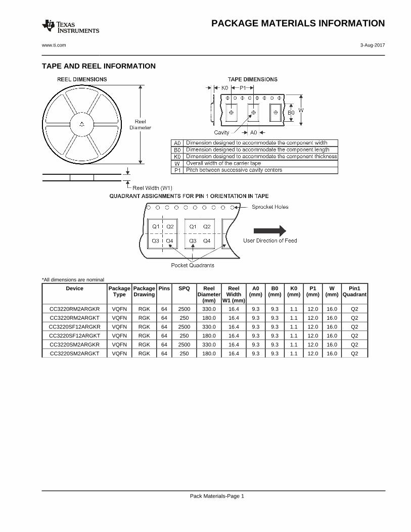
TAPE AND REEL INFORMATION
*All dimensions are nominal
Device PackageType
PackageDrawing
Pins SPQ ReelDiameter
(mm)
ReelWidth
W1 (mm)
A0(mm)
B0(mm)
K0(mm)
P1(mm)
W(mm)
Pin1Quadrant
CC3220RM2ARGKR VQFN RGK 64 2500 330.0 16.4 9.3 9.3 1.1 12.0 16.0 Q2
CC3220RM2ARGKT VQFN RGK 64 250 180.0 16.4 9.3 9.3 1.1 12.0 16.0 Q2
CC3220SF12ARGKR VQFN RGK 64 2500 330.0 16.4 9.3 9.3 1.1 12.0 16.0 Q2
CC3220SF12ARGKT VQFN RGK 64 250 180.0 16.4 9.3 9.3 1.1 12.0 16.0 Q2
CC3220SM2ARGKR VQFN RGK 64 2500 330.0 16.4 9.3 9.3 1.1 12.0 16.0 Q2
CC3220SM2ARGKT VQFN RGK 64 250 180.0 16.4 9.3 9.3 1.1 12.0 16.0 Q2
PACKAGE MATERIALS INFORMATION
www.ti.com 3-Aug-2017
Pack Materials-Page 1
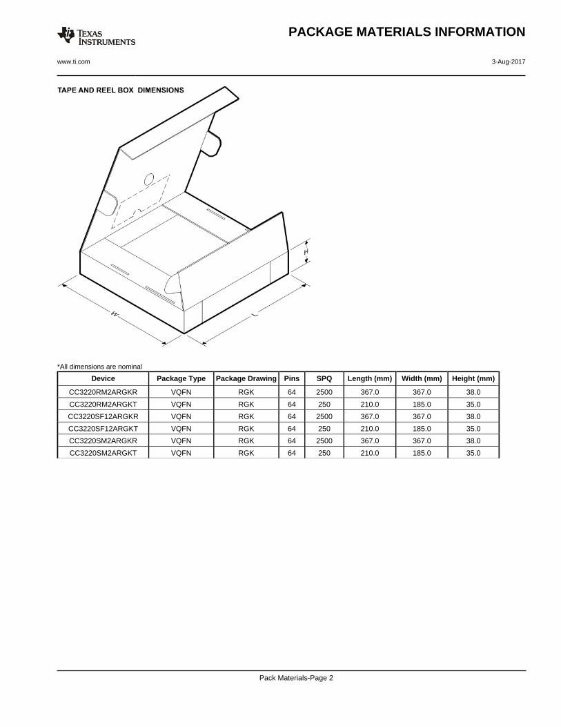
*All dimensions are nominal
Device Package Type Package Drawing Pins SPQ Length (mm) Width (mm) Height (mm)
CC3220RM2ARGKR VQFN RGK 64 2500 367.0 367.0 38.0
CC3220RM2ARGKT VQFN RGK 64 250 210.0 185.0 35.0
CC3220SF12ARGKR VQFN RGK 64 2500 367.0 367.0 38.0
CC3220SF12ARGKT VQFN RGK 64 250 210.0 185.0 35.0
CC3220SM2ARGKR VQFN RGK 64 2500 367.0 367.0 38.0
CC3220SM2ARGKT VQFN RGK 64 250 210.0 185.0 35.0
PACKAGE MATERIALS INFORMATION
www.ti.com 3-Aug-2017
Pack Materials-Page 2
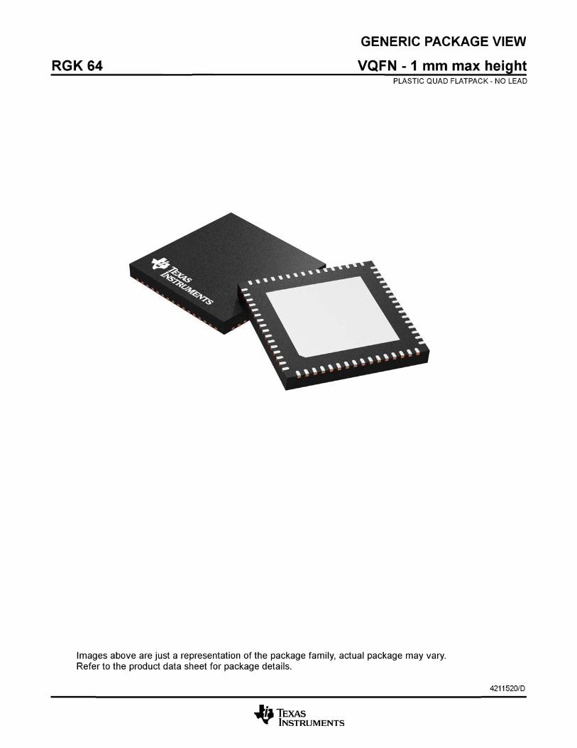
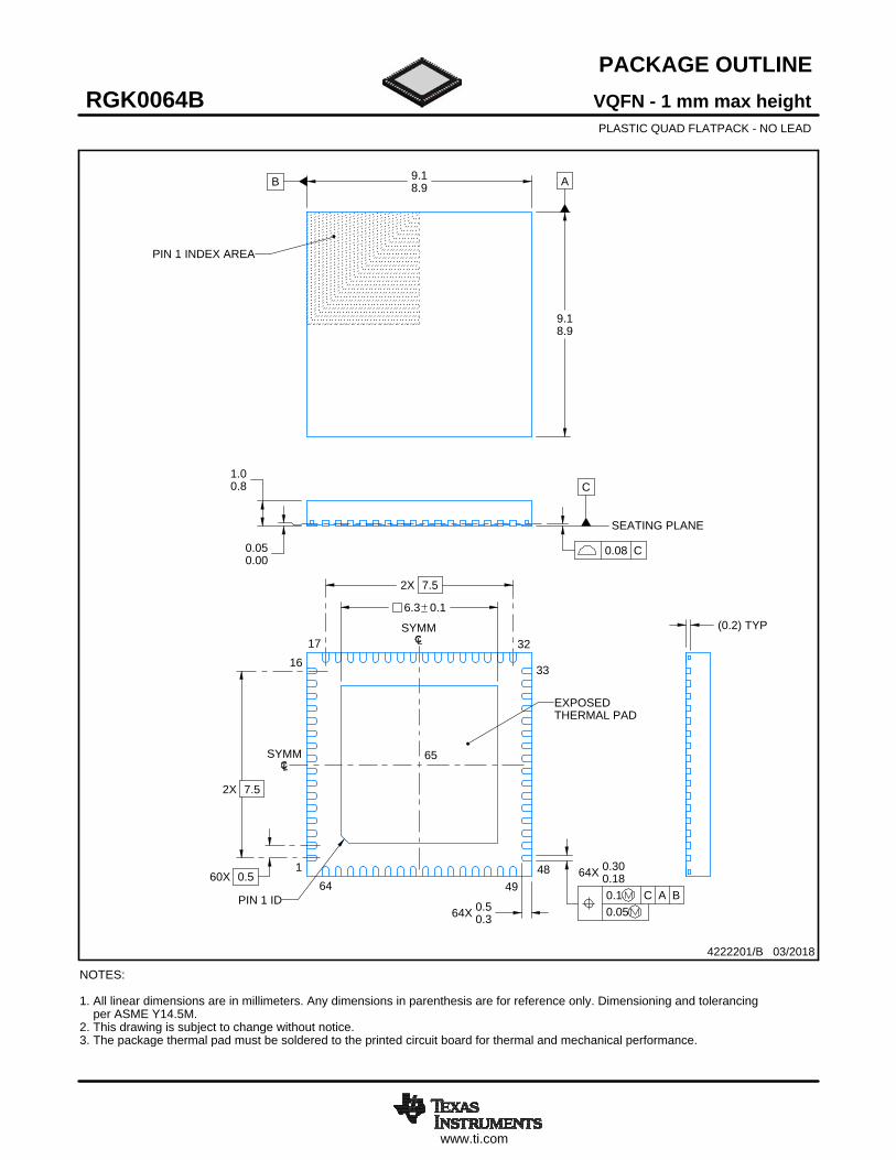
www.ti.com
PACKAGE OUTLINE
C
9.18.9
9.18.9
1.00.8
0.050.00
2X 7.5
60X 0.5
2X 7.5
64X 0.50.3
64X 0.300.18
6.3 0.1(0.2) TYP
VQFN - 1 mm max heightRGK0064BPLASTIC QUAD FLATPACK - NO LEAD
4222201/B 03/2018
0.08 C
0.1 C A B0.05
NOTES: 1. All linear dimensions are in millimeters. Any dimensions in parenthesis are for reference only. Dimensioning and tolerancing per ASME Y14.5M. 2. This drawing is subject to change without notice. 3. The package thermal pad must be soldered to the printed circuit board for thermal and mechanical performance.
PIN 1 INDEX AREA
SEATING PLANE
PIN 1 ID
SYMM
EXPOSEDTHERMAL PAD
SYMM
1
1617 32
33
484964
65
SCALE 1.500
AB
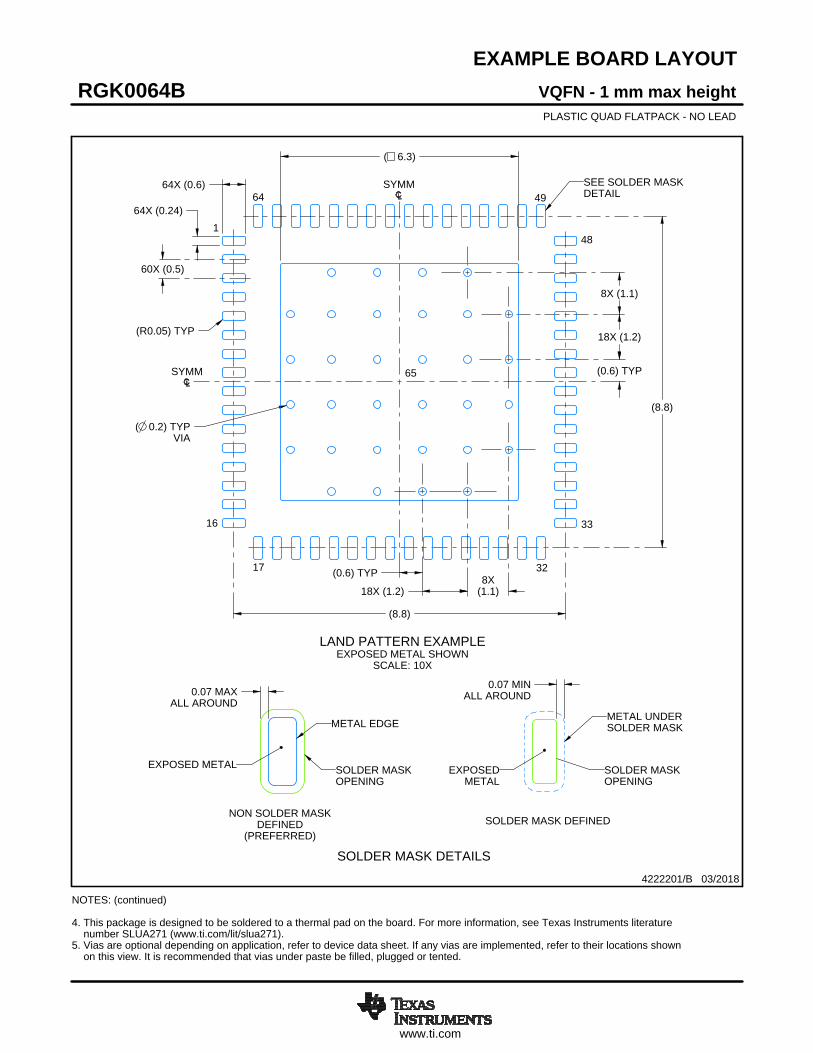
www.ti.com
EXAMPLE BOARD LAYOUT
60X (0.5)
( 0.2) TYPVIA
(R0.05) TYP
0.07 MAXALL AROUND
0.07 MINALL AROUND
64X (0.6)
64X (0.24)
(8.8)
(8.8)
( 6.3)
(0.6) TYP
18X (1.2)
8X (1.1)
(0.6) TYP
18X (1.2)8X
(1.1)
VQFN - 1 mm max heightRGK0064BPLASTIC QUAD FLATPACK - NO LEAD
4222201/B 03/2018
NOTES: (continued) 4. This package is designed to be soldered to a thermal pad on the board. For more information, see Texas Instruments literature number SLUA271 (www.ti.com/lit/slua271).5. Vias are optional depending on application, refer to device data sheet. If any vias are implemented, refer to their locations shown on this view. It is recommended that vias under paste be filled, plugged or tented.
SYMM
SYMM
LAND PATTERN EXAMPLEEXPOSED METAL SHOWN
SCALE: 10X
SEE SOLDER MASKDETAIL
1
16
17 32
33
48
4964
65
METAL EDGE
SOLDER MASKOPENING
EXPOSED METAL
METAL UNDERSOLDER MASK
SOLDER MASKOPENING
EXPOSEDMETAL
NON SOLDER MASKDEFINED
(PREFERRED)SOLDER MASK DEFINED
SOLDER MASK DETAILS
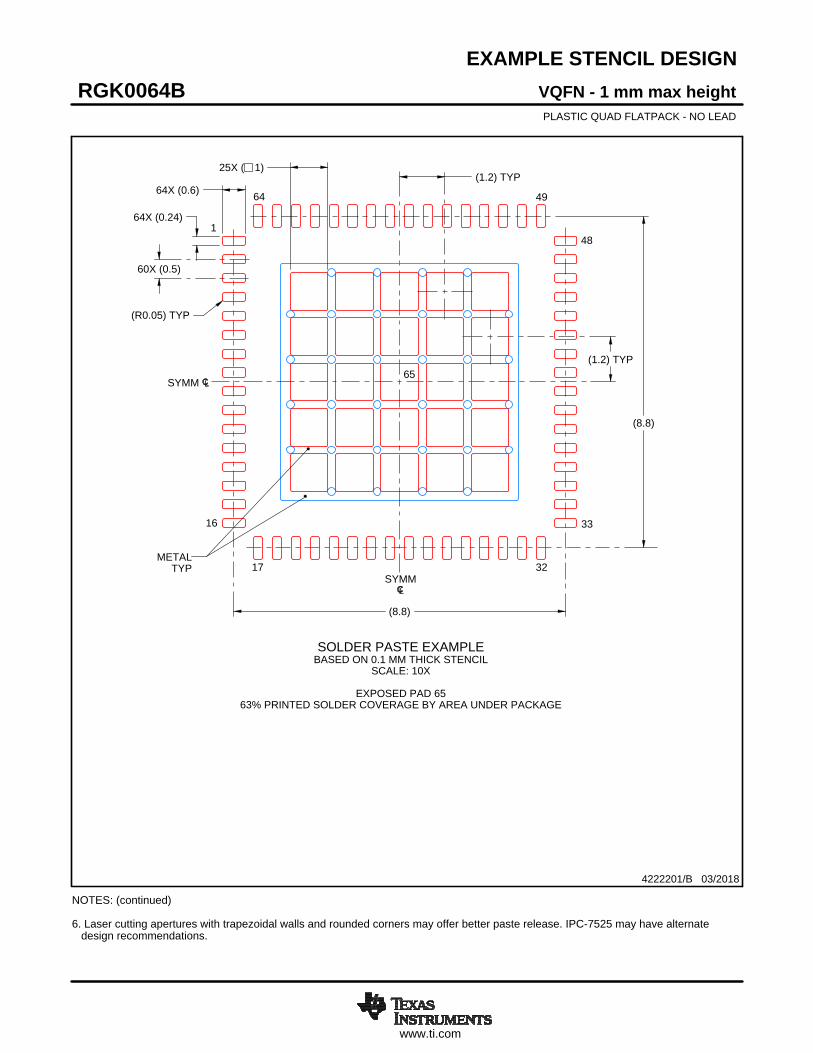
www.ti.com
EXAMPLE STENCIL DESIGN
64X (0.6)
64X (0.24)
60X (0.5)
(8.8)
(8.8)
25X ( 1)
(R0.05) TYP
(1.2) TYP
(1.2) TYP
VQFN - 1 mm max heightRGK0064BPLASTIC QUAD FLATPACK - NO LEAD
4222201/B 03/2018
NOTES: (continued) 6. Laser cutting apertures with trapezoidal walls and rounded corners may offer better paste release. IPC-7525 may have alternate design recommendations.
SOLDER PASTE EXAMPLEBASED ON 0.1 MM THICK STENCIL
SCALE: 10X
EXPOSED PAD 6563% PRINTED SOLDER COVERAGE BY AREA UNDER PACKAGE
SYMM
SYMM
1
16
17 32
33
48
4964
65
METALTYP
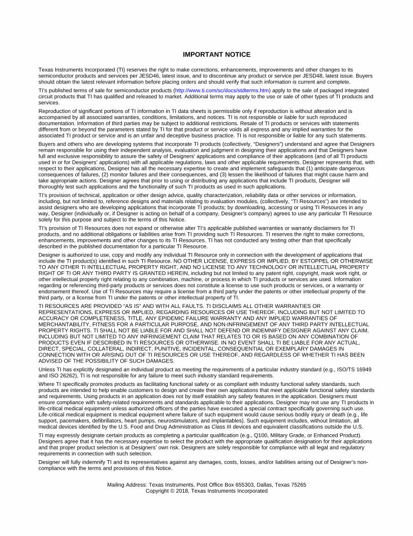
IMPORTANT NOTICE
Texas Instruments Incorporated (TI) reserves the right to make corrections, enhancements, improvements and other changes to itssemiconductor products and services per JESD46, latest issue, and to discontinue any product or service per JESD48, latest issue. Buyersshould obtain the latest relevant information before placing orders and should verify that such information is current and complete.TI’s published terms of sale for semiconductor products (http://www.ti.com/sc/docs/stdterms.htm) apply to the sale of packaged integratedcircuit products that TI has qualified and released to market. Additional terms may apply to the use or sale of other types of TI products andservices.Reproduction of significant portions of TI information in TI data sheets is permissible only if reproduction is without alteration and isaccompanied by all associated warranties, conditions, limitations, and notices. TI is not responsible or liable for such reproduceddocumentation. Information of third parties may be subject to additional restrictions. Resale of TI products or services with statementsdifferent from or beyond the parameters stated by TI for that product or service voids all express and any implied warranties for theassociated TI product or service and is an unfair and deceptive business practice. TI is not responsible or liable for any such statements.Buyers and others who are developing systems that incorporate TI products (collectively, “Designers”) understand and agree that Designersremain responsible for using their independent analysis, evaluation and judgment in designing their applications and that Designers havefull and exclusive responsibility to assure the safety of Designers' applications and compliance of their applications (and of all TI productsused in or for Designers’ applications) with all applicable regulations, laws and other applicable requirements. Designer represents that, withrespect to their applications, Designer has all the necessary expertise to create and implement safeguards that (1) anticipate dangerousconsequences of failures, (2) monitor failures and their consequences, and (3) lessen the likelihood of failures that might cause harm andtake appropriate actions. Designer agrees that prior to using or distributing any applications that include TI products, Designer willthoroughly test such applications and the functionality of such TI products as used in such applications.TI’s provision of technical, application or other design advice, quality characterization, reliability data or other services or information,including, but not limited to, reference designs and materials relating to evaluation modules, (collectively, “TI Resources”) are intended toassist designers who are developing applications that incorporate TI products; by downloading, accessing or using TI Resources in anyway, Designer (individually or, if Designer is acting on behalf of a company, Designer’s company) agrees to use any particular TI Resourcesolely for this purpose and subject to the terms of this Notice.TI’s provision of TI Resources does not expand or otherwise alter TI’s applicable published warranties or warranty disclaimers for TIproducts, and no additional obligations or liabilities arise from TI providing such TI Resources. TI reserves the right to make corrections,enhancements, improvements and other changes to its TI Resources. TI has not conducted any testing other than that specificallydescribed in the published documentation for a particular TI Resource.Designer is authorized to use, copy and modify any individual TI Resource only in connection with the development of applications thatinclude the TI product(s) identified in such TI Resource. NO OTHER LICENSE, EXPRESS OR IMPLIED, BY ESTOPPEL OR OTHERWISETO ANY OTHER TI INTELLECTUAL PROPERTY RIGHT, AND NO LICENSE TO ANY TECHNOLOGY OR INTELLECTUAL PROPERTYRIGHT OF TI OR ANY THIRD PARTY IS GRANTED HEREIN, including but not limited to any patent right, copyright, mask work right, orother intellectual property right relating to any combination, machine, or process in which TI products or services are used. Informationregarding or referencing third-party products or services does not constitute a license to use such products or services, or a warranty orendorsement thereof. Use of TI Resources may require a license from a third party under the patents or other intellectual property of thethird party, or a license from TI under the patents or other intellectual property of TI.TI RESOURCES ARE PROVIDED “AS IS” AND WITH ALL FAULTS. TI DISCLAIMS ALL OTHER WARRANTIES ORREPRESENTATIONS, EXPRESS OR IMPLIED, REGARDING RESOURCES OR USE THEREOF, INCLUDING BUT NOT LIMITED TOACCURACY OR COMPLETENESS, TITLE, ANY EPIDEMIC FAILURE WARRANTY AND ANY IMPLIED WARRANTIES OFMERCHANTABILITY, FITNESS FOR A PARTICULAR PURPOSE, AND NON-INFRINGEMENT OF ANY THIRD PARTY INTELLECTUALPROPERTY RIGHTS. TI SHALL NOT BE LIABLE FOR AND SHALL NOT DEFEND OR INDEMNIFY DESIGNER AGAINST ANY CLAIM,INCLUDING BUT NOT LIMITED TO ANY INFRINGEMENT CLAIM THAT RELATES TO OR IS BASED ON ANY COMBINATION OFPRODUCTS EVEN IF DESCRIBED IN TI RESOURCES OR OTHERWISE. IN NO EVENT SHALL TI BE LIABLE FOR ANY ACTUAL,DIRECT, SPECIAL, COLLATERAL, INDIRECT, PUNITIVE, INCIDENTAL, CONSEQUENTIAL OR EXEMPLARY DAMAGES INCONNECTION WITH OR ARISING OUT OF TI RESOURCES OR USE THEREOF, AND REGARDLESS OF WHETHER TI HAS BEENADVISED OF THE POSSIBILITY OF SUCH DAMAGES.Unless TI has explicitly designated an individual product as meeting the requirements of a particular industry standard (e.g., ISO/TS 16949and ISO 26262), TI is not responsible for any failure to meet such industry standard requirements.Where TI specifically promotes products as facilitating functional safety or as compliant with industry functional safety standards, suchproducts are intended to help enable customers to design and create their own applications that meet applicable functional safety standardsand requirements. Using products in an application does not by itself establish any safety features in the application. Designers mustensure compliance with safety-related requirements and standards applicable to their applications. Designer may not use any TI products inlife-critical medical equipment unless authorized officers of the parties have executed a special contract specifically governing such use.Life-critical medical equipment is medical equipment where failure of such equipment would cause serious bodily injury or death (e.g., lifesupport, pacemakers, defibrillators, heart pumps, neurostimulators, and implantables). Such equipment includes, without limitation, allmedical devices identified by the U.S. Food and Drug Administration as Class III devices and equivalent classifications outside the U.S.TI may expressly designate certain products as completing a particular qualification (e.g., Q100, Military Grade, or Enhanced Product).Designers agree that it has the necessary expertise to select the product with the appropriate qualification designation for their applicationsand that proper product selection is at Designers’ own risk. Designers are solely responsible for compliance with all legal and regulatoryrequirements in connection with such selection.Designer will fully indemnify TI and its representatives against any damages, costs, losses, and/or liabilities arising out of Designer’s non-compliance with the terms and provisions of this Notice.
Mailing Address: Texas Instruments, Post Office Box 655303, Dallas, Texas 75265Copyright © 2018, Texas Instruments Incorporated