
Supporting Online Material for -...
18
www.sciencemag.org/cgi/content/full/325/5940/594/DC1 Supporting Online Material for Ultrasmooth Patterned Metals for Plasmonics and Metamaterials Prashant Nagpal, Nathan C. Lindquist, Sang-Hyun Oh, David J. Norris* *To whom correspondence should be addressed. E-mail: [email protected] Published 31 July 2009, Science 325, 594 (2009) DOI: 10.1126/science.1174655 This PDF file includes: Materials and Methods Figs. S1 to S7 Tables S1 to S3 References
Transcript of Supporting Online Material for -...
www.sciencemag.org/cgi/content/full/325/5940/594/DC1
Supporting Online Material for
Ultrasmooth Patterned Metals for Plasmonics and Metamaterials
Prashant Nagpal, Nathan C. Lindquist, Sang-Hyun Oh, David J. Norris*
*To whom correspondence should be addressed. E-mail: [email protected]
Published 31 July 2009, Science 325, 594 (2009)
DOI: 10.1126/science.1174655
This PDF file includes:
Materials and Methods Figs. S1 to S7 Tables S1 to S3 References

1
Ultra-Smooth Patterned Metals for Plasmonics and Metamaterials
Prashant Nagpal,1 Nathan C. Lindquist,2 Sang-Hyun Oh,2 David J. Norris1,*
1Department of Chemical Engineering & Materials Science, University of Minnesota Minneapolis, MN 55455 USA
2Department of Electrical and Computer Engineering, University of Minnesota Minneapolis, MN 55455 USA
*To whom correspondence should be addressed: [email protected]
Supporting Online Material
1. Materials and Methods
A. Fabrication of patterned silicon templates
i. Using focused ion beam (FIB)
Maskless lithography of the desired surface pattern was performed on smooth single-crystal silicon wafers using a dual-beam FEI Quanta 200 3D FIB workstation. The patterns were etched using 30 kV as the acceleration voltage and 100 pA as the ion beam current. The patterned silicon wafers were then cleaned in a freshly prepared 1:1 solution (by volume) of sulfuric acid and hydrogen peroxide (piranha etch) for 5 minutes to remove any organic contamination. ii. Using optical lithography
Single-crystal silicon wafers with the desired crystal orientation were coated with Shipley 1805 positive-tone photoresist using spin coating at 5000 rpm. Before exposure, the resist was baked at 105 °C for 60 seconds. The desired pattern was then obtained by exposing the resist through a chrome-on-glass photomask using a Karl Suss MABA6 mask aligner. The exposed resist was developed for 30 seconds in a 17% solution (by volume) of Shipley 351 developer in water. The patterned wafer was coated with a thin layer of chromium or tungsten using sputtering or thermal evaporation and the wafer was placed in acetone under mild sonication for lift-off. The resulting patterned metal film was used as a mask for anisotropic KOH etching or reactive ion etching (RIE). For KOH etching, [100]-oriented silicon wafers were utilized. To obtain the linear gratings in Fig. 4A, the mask was patterned with lines oriented along [110] of the wafer. To obtain pyramidal divets for templating the structures in Fig. 2C, 2D, and 2E, the mask was patterned with squares aligned along [110] or an array of circles aligned along [110]. These grooves or divets were obtained by anisotropic

2
etching with the following procedure. After a 10 second soak in buffered oxide etchant to remove any native oxide layer, the wafer was immersed in a 25 wt% solution of KOH in water at 80 °C. The time varied depending on the exact pattern to be etched. For Fig. 2C and 2D, the immersion time was 15 minutes. The wafers were then cleaned in deionized water for 30 minutes to remove any residual KOH. To remove the metal mask, CR-7S etchant (Cyantek corp.) or hydrogen peroxide were used for chromium and tungsten, respectively. Finally, the wafers were placed in piranha etch for 5 minutes as a final cleaning step before the deposition of metal in the template-stripping process. iii. Using nanosphere lithography
Nearly monodisperse 450 nm diameter polystyrene spheres were synthesized using a published procedure (S1). A 20 weight % aqueous dispersion of these spheres was then spin-coated onto a clean silicon wafer to obtain a close-packed monolayer. After heating the wafer in an oven at 105 °C for 30 minutes, it was treated in an oxygen plasma using an STS etcher. This process shrunk the spheres while maintaining the center-to-center distance between nearest neighbors, which was set by the initial size of the colloidal spheres. Alumina or silica was then deposited to obtain a mask with holes via lift-off. This mask was used to transfer the hole-array pattern into the underlying single-crystal silicon wafer. Specifically, deep reactive ion etching (DRIE) was performed with a three-step Bosch process with a cycle that consisted of 5 seconds of passivation, 3 seconds of etching, and 7 seconds of patterning using SF6, C4F8, and argon gases, 800 W for the coil power, and 15 W for the platen power. This cycle was repeated until the desired depth was achieved (typically ~2 μm). The etched templates were then cleaned for 2 minutes using a 1:1 solution (by volume) of ammonium hydroxide and hydrogen peroxide to eliminate a Teflon-like film. This was followed by an oxide etch to remove the dielectric mask. For example, silica was etched away by immersing for 1 minute in 5% aqueous hydrofluoric acid. Finally, the wafers were placed in piranha etch for 5 minutes as a final cleaning step before the deposition of metal in the template-stripping process.
B. Template stripping of patterned metal films
i. Metal deposition
The patterned single-crystal silicon wafer could be coated with the desired metal (silver, gold, or copper) using thermal evaporation or sputtering. Typically, a thermal evaporator with a pressure of less than 10-5 Torr was used with metal deposition rates from 0.2-0.4 nm/second. In this case, the substrate was at room temperature. To produce the silver nanohole array in Fig. 2F, metal was thermally evaporated with near vertical deposition to obtain clean edges. For silver films, the roughness could be decreased further by heating the substrate during evaporation to 75 °C and decreasing the deposition rate to 0.01-0.02 nm/second. ii. Template-stripping with epoxy
A two-part epoxy was applied (or spin coated) to the deposited metal to form a removal layer of the desired thickness. Alternatively, the epoxy could be used as an adhesive layer to attach another substrate (silicon or glass). Typically, we used either a 1:1 weight % mixture of a two-part epoxy (EPO-TEK 377, Epoxy Technologies) or a two-part quick-set epoxy

3
(Loctite). The epoxy could be cured thermally or with ultraviolet light. Typically, the sample was placed in an oven at 150 °C for one hour. This had the added benefit of increasing the grain size, as shown in Fig. S5. After curing, the epoxy was removed from the silicon template by using a razor blade to gently lift one edge and then peeling it off. iii. Template-stripping with electrodeposited films
After the patterned silicon templates were coated with a thin layer of evaporated metal (typically 200 nm thick), they were immersed in an electrolyte solution, along with a platinum wire as a counter electrode and lithium acetate as a reference electrode. Solutions of 1M CuSO4 (pH 2 adjusted with H2SO4) and ammoniacal silver nitrate (pH 10 using NH4OH) were used to electrodeposit copper and silver, respectively. After a sufficient thickness of metal was electrodeposited (greater than ~50 μm), the entire film could be peeled off the silicon. iv. Template-stripping of multilayer films
Starting with any of the patterned silicon templates (bull’s eyes, grooves, bump arrays, pyramidal divets, and hole arrays), multilayer films could be obtained with template stripping. Typically, 30 nm of silver was thermally evaporated (at 0.1-0.2 nm/second) onto a clean patterned wafer. Alternating layers of alumina (15 nm thick deposited at 0.01 nm/second) and silver (30 nm thick deposited at 0.5 nm/second) were then deposited with an AJA sputterer. After the desired number of layers were formed, the film was removed using either epoxy or an electrodeposited film, as described above. v. Thermal annealing of gold films
To increase the grain size of our gold films, they were placed in a pre-heated oven at 500 °C for 5 minutes. The oven was in a nitrogen-containing glove box and the sample was cooled to room temperature before it was brought into the ambient and template-stripped. vi. Avoiding sample contamination
Due to concerns over the potential corrosion of our silver films, especially due to sulfur compounds, samples were used immediately whenever possible. Samples were typically template-stripped immediately prior to the measurements. If longer term storage was necessary, they were kept in a nitrogen-containing glove box.
C. Characterization
i. X-ray photoelectron spectroscopy (XPS)
Characterization of surface impurities was performed on a custom XPS spectrometer. The samples were thoroughly cleaned before the measurements to minimize any organic contamination and placed in a high vacuum chamber (base pressure ~10-9 Torr). The X-ray source (Mg, 1253.6 eV) was at an angle of 5° from normal to the sample and the photoelectrons were detected at an angle of 54.7° from normal (Phi 540 detector). 200 W (15 kV) was applied to the source and the signal was collected from the sample with no bias voltage applied. The analyzer pass energy for the survey scan was 89.45 eV and a higher

4
resolution scan was done to determine the surface composition. The pass energy for the high resolution scan was 17.9 eV. ii. Ellipsometry
To determine the dielectric function of our films, a VASE spectroscopic ellipsometer (JA Woolam Co.) was utilized. With a 75 W xenon lamp source, the ratio of the polarized light reflected from the sample (s and p polarization) was determined. We then extracted the stokes parameters Ψ and Δ using the equation,
i
s
p er
r)tan( .
With WVASE software (JA Woolam Co.), we fit the dielectric functions using numerical iteration and the Fresnel equations. The measurements and fitting were performed for a wavelength interval of 1 nm and all the iterations were run to a mean square error less than 0.5. The wavelength range for the silver and gold films were 450 to 750 nm and 550 to 850 nm, respectively. iii. Measurement of the plasmon propagation length
The plasmon propagation lengths were measured for two films: (a) a 200 nm thick template-stripped ultra-smooth silver film on epoxy and (b) a 200 nm thick as-deposited rough silver film on a glass slide. Silicon could not be used as the control substrate because optical transparency was required. Both films had been evaporated onto their respective substrates at room temperature at a deposition rate of 0.2-0.4 nm/second. The root mean square roughnesses for these surfaces were approximately 0.7 and 5.0 nm, respectively. For each, multiple slit-groove pairs (like that shown in Fig. 3A) were milled into the film with FIB. Both the slit and the groove were approximately 200 nm wide. Separation distances between the slit and groove were set at 10, 12, 15, 20, 25, 30, 35, and 40 μm. Each sample was then mounted on a Nikon TE 200 inverted microscope (40X objective, numerical aperture of 0.6) and illuminated on the epoxy or glass side in transmission mode with light from a quartz tungsten halogen lamp focused by a condenser (numerical aperture of 0.9). Surface plasmons were launched on the silver film when light passed through the slits. When these propagating plasmons struck the grooves, they scattered light that could be collected by the microscope objective. For each groove separately, we projected the image of the scattered light onto the entrance of an imaging monochromator (TRIAX 320, Jobin Yvon) and measured the spectrum with a liquid-nitrogen-cooled spectroscopic CCD camera (Princeton Instruments). Light that was transmitted directly through the slits in the sample was not allowed to enter the monochromator. Plots of the scattered intensity versus slit-groove separation distance for a particular wavelength were then used to extract the wavelength dependence of the surface plasmon propagation lengths (see Section 1.D.i below). iv. Atomic force microscopy (AFM)
All AFM images were obtained with a Veeco Nanoscope IIIA multimode system that was housed inside a nitrogen-containing glove box. The samples were scanned using tapping mode, typically over a 5x5 μm2 area at a scan rate of 1 Hz. Nanoscope software was utilized

5
to analyze the images and extract topographical information, including the root mean square (rms) surface roughness and the spectral density function (sdf). v. Confocal Raman microscopy
Confocal Raman scans were performed on a Witec Alpha 300R system equipped with an Omnichrome 514 nm argon-ion laser. The spectral range of the scan was between 0 and 4000 cm-1 with a resolution of 0.02 cm-1. The spatial resolution of the confocal system was 250 nm in the scanning plane and 500 nm in the perpendicular direction.
D. Analysis
i. Experimental surface plasmon propagation lengths
For each wavelength, the scattered intensity versus slit-groove separation, d, was fitted to the following equation (S2),
/( ) SPPx Lb oI x I I e ,
where LSPP is the surface plasmon propagation length, Io is the surface plasmon intensity at the slit, and Ib is a background intensity. We note that this is an underestimate of the surface plasmon propagation length since not all surface plasmons will propagate along the shortest path between the slit and groove (S2). This angular dependence is ignored here because an exact treatment, which should include both the finite length of the slit-groove pair and knowledge of the angular dependence of the surface plasmon scattering, is not available. Approximate treatments lead to an overestimation of LSPP (S2). A nonlinear regression analysis yielded an estimate of the surface plasmon propagation length with the standard errors shown in Fig. 3B. (The errors for the control film were smaller than the symbols used to plot the data and are therefore not shown.) Values for the expected propagation lengths were obtained by extracting the dielectric constants via ellipsometry for samples treated to the same conditions and inserting these into the following formulae (S3),
1
1 1(2 Im( )) Im( )
2( / ) 1metal
SPP xmetal
L kc
,
where kx is the in-plane wavevector of the surface plasmon along the direction of propagation. Note that these equations assume that the only loss mechanism for plasmon propagation is due to ohmic losses in the metal. (This is equivalent to Lohm below in Section 1.D.ii. and in the main text.) ii. Calculation of the total propagation length Ltot
Surface plasmon propagation lengths due to in-plane scattering of surface plasmons, Lscat, and scattering of surface plasmons into radiation, Lrad, were estimated using the following equations,

6
'
5 2 2
1/2'
5 2 2
2 1
3 ( / )
3 1
4 ( / )
metal
scat
metal
rad
Lc
Lc
,
where ’metal is the real part of the dielectric function of the metal, is the correlation length
of the surface corrugation and is the root mean square height (S3, S4). Values for and were estimated from atomic force microscopy (AFM) measurements of the films. From an AFM scan, the power spectral density function (sdf) was determined and fit to a Gaussian. By plotting ln(sdf) versus the wavevector squared, and were extracted from the slope and peak value. [See (S3) for more details.] The total propagation length was calculated using,
1 1 1 1
tot ohm scat radL L L L ,
where Lohm is due to ohmic losses in the metal and Ltot is the expected surface plasmon propagation length that includes ohmic losses in the metal, in-plane scattering of surface plasmons, and radiative scattering of surface plasmons. Such values are estimated in Table S2 based on the and parameters listed in Table S1.
When grain boundaries were considered (Table S3), the total propagation length was determined from,
1 1 1 1 1
tot ohm scat rad gbL L L L L ,
where Lgb is the propagation length due to scattering of surface plasmons from grain boundaries. Following (S5), we estimated Lgb as dgb/Sgb, where dgb is the average grain diameter and Sgb is a scattering coefficient. We set Sgb equal to 0.2% based on measurements in (S5).

7
2. Supplementary Figures
Fig. S1 Experimental reflectivity spectrum (red curve) of a template-stripped silver bull’s eye similar to that in Fig. 1C. An inverted optical microscope illuminated the bull’s eye with white light. The reflected signal was collected through the microscope objective and imaged onto the input of a fiber-optic-coupled ultraviolet-visible spectrophotometer. An aperture between the sample and the objective limited the collection angle to +/- 1.2° from normal. The reflectivity was normalized with the signal collected from a flat portion of the silver film next to the bull’s eye. A simulation (black dashed curve) was obtained using parameters (580 nm period, 50 nm ridge height, and 220 nm ridge width) estimated from electron micrographs of the real structure. The theoretical peak shape was found to be very sensitive to the exact structure. The estimated cross section of the ridges used in the simulation is shown in the inset. The calculated reflectivity was obtained using the finite difference time domain method and a non-uniform mesh with a 5 nm nominal grid size above and below the air/silver interface and a 0.5 nm grid size at this interface. A simulated broadband pulse that contained wavelengths from 450 to 750 nm impinged on the structure and the reflected power was Fourier transformed (with zero padding after the signal had decreased to 10-9 of the original power). To decrease the computation time, the calculation was performed on an infinite linear grating and its response was averaged over all angles (applicable for a large bull’s eye). To compare with experiment, which utilized unpolarized light, the TE and TM response was averaged and normalized by the reflected power from a perfectly flat silver film.

8
Fig. S2 The real component of the dielectric function, ’, extracted via ellipsometry for two representative silver films. Blue curve: the smooth surface of a 250 nm thick template-stripped film deposited by thermal evaporation onto a silicon wafer at room temperature. Red curve: the smooth surface of a 250 nm thick template-stripped film deposited by slow thermal evaporation onto a silicon wafer heated to ~75 °C. For comparison, ’ values reported by Palik (S6) and Johnson and Christy (S7) are shown by the black dashed and black solid curves, respectively. Due to strong overlap with the blue curve, the black curve is mostly concealed.

9
Fig. S3 The imaginary component of the dielectric function, ’’, extracted via ellipsometry for two representative silver films. Blue curve: the smooth surface of a 250 nm thick template-stripped film deposited by thermal evaporation onto a silicon wafer at room temperature. Red curve: the smooth surface of a 250 nm thick template-stripped film deposited by slow thermal evaporation onto a silicon wafer heated to ~75 °C. For comparison, ’’ values reported by Palik (S6) and Johnson and Christy (S7) are shown by the black dashed and black solid curves, respectively.

10
Fig. S4 The ohmic propagation lengths, Lohm, for surface plasmons versus wavelength for two
representative silver films. These propagation lengths are calculated from the dielectric functions measured via ellipsometry that are shown in Figs. S2 and S3. Blue curve: the smooth surface of a 250 nm thick template-stripped film deposited by thermal evaporation onto a silicon wafer at room temperature. Red curve: the smooth surface of a 250 nm thick template-stripped film deposited by slow thermal evaporation onto a silicon wafer heated to ~75 °C. For comparison, Lohm values reported by Palik (S6) and Johnson and Christy (S7) are shown by the black dashed and black solid curves, respectively.

11
Fig. S5 Atomic force microscopy images of a 250 nm thick silver film before (A) and after (B)
template stripping. The metal was thermally evaporated slowly onto a silicon wafer at 75 °C. In (A), the top (rough) surface is imaged. In (B), the templated (smooth) interface is imaged. The grain size increased between (A) and (B) because the epoxy used to template-strip the film was thermally cured at 150 °C for one hour. Roughness parameters extracted for these samples are shown in Table S1.
A
B

12
Fig. S6 Atomic force microscopy images of a 200 nm thick gold film before (A) and after (B)
template stripping. The metal was thermally evaporated onto a silicon wafer at room temperature. In (A), the top (rough) surface is imaged. In (B), the templated (smooth) interface is imaged. To increase the grain size, a rapid thermal anneal (5 minutes at 500 °C) was performed before template-stripping. This treatment was performed after the image in (A) was taken. Roughness parameters extracted from these samples are shown in Table S1.
A
B
13
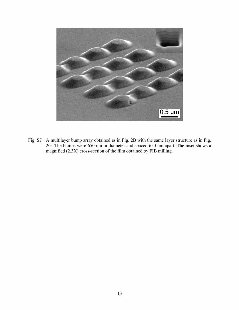
Fig. S7 A multilayer bump array obtained as in Fig. 2B with the same layer structure as in Fig. 2G. The bumps were 650 nm in diameter and spaced 650 nm apart. The inset shows a magnified (2.3X) cross-section of the film obtained by FIB milling.

14
3. Supplementary Tables:
Table S1. Surface corrugation parameters, and , extracted from atomic force microscopy (AFM) images for different metal surfaces. Following (S3, S4), is the correlation length and is the root mean square height. Both can be estimated from a Gaussian fit to the spectral density function obtained from the AFM image. The rms roughness extracted directly from the AFM scan is shown for comparison. The four surfaces shown in Figs. S5 and S6 were measured. These represent the rough (top) surface of a slow-evaporated 250 nm silver film, the smooth template-stripped interface from the same slow-evaporated silver film, the rough (top) surface of an evaporated 200 nm film of gold, and the smooth template-stripped interface from the same evaporated gold film. The smooth silver film was exposed to 1 hour at 150 °C to cure the epoxy. The smooth gold sample was annealed for 5 minutes at 500 °C prior to template-stripping. Both of these heat treatments increased the grain size.
Material (nm) (nm) Measured root mean square roughness from AFM (nm)
Rough Silver
179 6.56 4.7
Smooth Silver
52.9 0.941 0.36
Rough Gold
92.4 1.59 1.6
Smooth
Gold 213 0.627 0.32

15
Table S2. Predicted propagation lengths based on our experimental measurements of the dielectric function (ellipsometry) and the surface corrugation (atomic force microscopy) for the four different metal surfaces shown in Figs. S5 and S6. We used formulas from (S3) to determine: (i) Lohm, due to ohmic loss in the metal, (ii) Lscat, due to in-plane scattering of the surface plasmons, (iii) Lrad, due to radiative scattering of the surface plasmons, and (iv) Ltot, the total effect of all of these loss channels. Note that the values obtained for the rough silver film are estimates due to the questionable validity of the single scattering approximation (S3) and potential complications in ellipsometry due to the rough interface. For Lscat and Lrad, we used the values of and listed in Table S1.
Material Wavelength Lohm (μm) Lscat (μm) Lrad (μm) Ltot (μm) 488 nm 7.47 10.2 4.19 2.12 514 nm 10.8 15.4 5.87 3.05 532 nm 13.5 20.2 7.33 3.85
Rough Silver
632 nm 33.7 75.2 21.7 11.2
488 nm 15.7 6.78 x 10³ 2.56 x 10³ 15.6 514 nm 22.1 1.03 x 10⁴ 3.58 x 10³ 21.9 532 nm 26.0 1.34 x 10⁴ 4.46 x 10³ 25.8
Smooth Silver
632 nm 54.1 4.94 x 10⁴ 1.32 x 10⁴ 53.8
Rough Gold
632 nm 10.5 427 139 9.52
Smooth
Gold 632 nm 11.8 4.72 x 10³ 1.52 x 10³ 11.7

16
Table S3. Predicted propagation lengths as in Table S2. In addition to Lohm, Lscat, and Lrad, the propagation length due to surface plasmon scattering at grain boundaries, Lgb, was included. Following (S5), we estimated Lgb as dgb/Sgb, where dgb is the average grain diameter and Sgb is a scattering coefficient. We set Sgb equal to 0.2% based on measurements in (S5). Ltot is the total effect of all of the loss channels. Values for the two gold surfaces in Fig. S6 are shown. For Lscat and Lrad, we used the values of and listed in Table S1.
Material Wavelength Lohm (μm) Lscat (μm) Lrad (μm) Lgb (μm) Ltot (μm) 632 nm 10.5 4.27 x 10² 1.39 x 10² 40.0 7.69 700 nm 27.7 1.02 x 10³ 2.77 x 10² 40.0 15.2
Rough Gold
800 nm 57.0 2.91 x 10³ 6.56 x 10² 40.0 22.5
632 nm 11.8 4.72 x 10³ 1.52 x 10³ 5.00 x 10² 11.4 700 nm 32.2 1.13 x 10⁴ 3.02 x 10³ 5.00 x 10² 29.9
Smooth Gold
800 nm 66.0 3.22 x 10⁴ 7.15 x 10³ 5.00 x 10² 57.7

17
4. References:
S1. B. T. Holland, C. F. Blanford, T. Do, A. Stein, Chem. Mater. 11, 795 (1999). S2. J. T. van Wijngaarden et al., Appl. Phys. Lett. 88, 3 (2006). S3. H. Raether, Surface Plasmons (Springer-Verlag, Berlin, 1988). S4. H. Shiba, M. Haraguchi, M. Fukui, J. Phys. Soc. Jpn. 63, 1400 (1994). S5. M. Kuttge et al., Appl. Phys. Lett. 93 (2008). S6. E. D. Palik, Ed., Handbook of Optical Constants of Solids (Academic Press, Orlando, 1985). S7. P. B. Johnson, R. W. Christy, Phys. Rev. B 6, 4370 (1972).