Supporting Online Material for -...
12
www.sciencemag.org/cgi/content/full/315/5814/966/DC1 Supporting Online Material for Experimental Realization of Wheeler’s Delayed-Choice Gedanken Experiment Vincent Jacques, E Wu, Frédéric Grosshans, François Treussart, Philippe Grangier, Alain Aspect, Jean-François Roch* *To whom correspondence should be addressed. E-mail: [email protected] Published 16 February 2007, Science 315, 966 (2007) DOI: 10.1126/science.1136303 This PDF file includes: Materials and Methods Figs. S1 to S4 References (Note: Figs. S1 to S4 are numbered below as Figs. 4 to 7, respectively)
Transcript of Supporting Online Material for -...
www.sciencemag.org/cgi/content/full/315/5814/966/DC1
Supporting Online Material for
Experimental Realization of Wheeler’s Delayed-Choice Gedanken
Experiment
Vincent Jacques, E Wu, Frédéric Grosshans, François Treussart, Philippe Grangier,
Alain Aspect, Jean-François Roch*
*To whom correspondence should be addressed. E-mail: [email protected]
Published 16 February 2007, Science 315, 966 (2007) DOI: 10.1126/science.1136303
This PDF file includes: Materials and Methods
Figs. S1 to S4
References
(Note: Figs. S1 to S4 are numbered below as Figs. 4 to 7, respectively)

Supplementary materials
Vincent Jacques1, E Wu1,2, Frederic Grosshans1, Francois Treussart1,Philippe Grangier3, Alain Aspect3, and Jean-Francois Roch1,∗
1Laboratoire de Photonique Quantique et Moleculaire, ENS de Cachan,
UMR CNRS 8537, Cachan, France2Key Laboratory of Optical and Magnetic Resonance Spectroscopy,
East China Normal University, Shanghai, China3Laboratoire Charles Fabry de l’Institut d’Optique, Campus Polytechnique,
UMR CNRS 8501, Palaiseau, France
∗ E-mail: [email protected]
1 Triggered single-photon source
We use a single nitrogen-vacancy (N-V) color center in a diamond nanocrystal. The N-V cen-
ters are created by irradiation of type Ib diamond sample with high-energy electrons followed
by annealing at800◦C 1. Under a well controlled irradiation dose, the N-V color center den-
sity is small enough to allow independent addressing of a single defect using standard confocal
microscopy2. The experimental setup used to excite and spectrally characterize single color
center photoluminescence is depicted on Fig. 4.
Excitation is done with a home-built pulsed laser at a wavelength of 532 nm3. The laser
system delivers 800 ps pulses with 50 pJ energy per pulse, high enough to ensure efficient
1C. Kurtsiefer, S. Mayer, P. Zarda, and H. Weinfurter,Phys. Rev. Lett.85, 290 (2000).2A. Gruber, A. Drabenstedt, C. Tietz, L. Fleury, J. Wrachtrup, and C. von Borczyskowski,Science276, 2012
(1997)3A. Beveratos, S. Kuhn, R. Brouri, T. Gacoin, J.-P. Poizat, and P. Grangier,Eur. Phys. J. D18, 191 (2002).
1
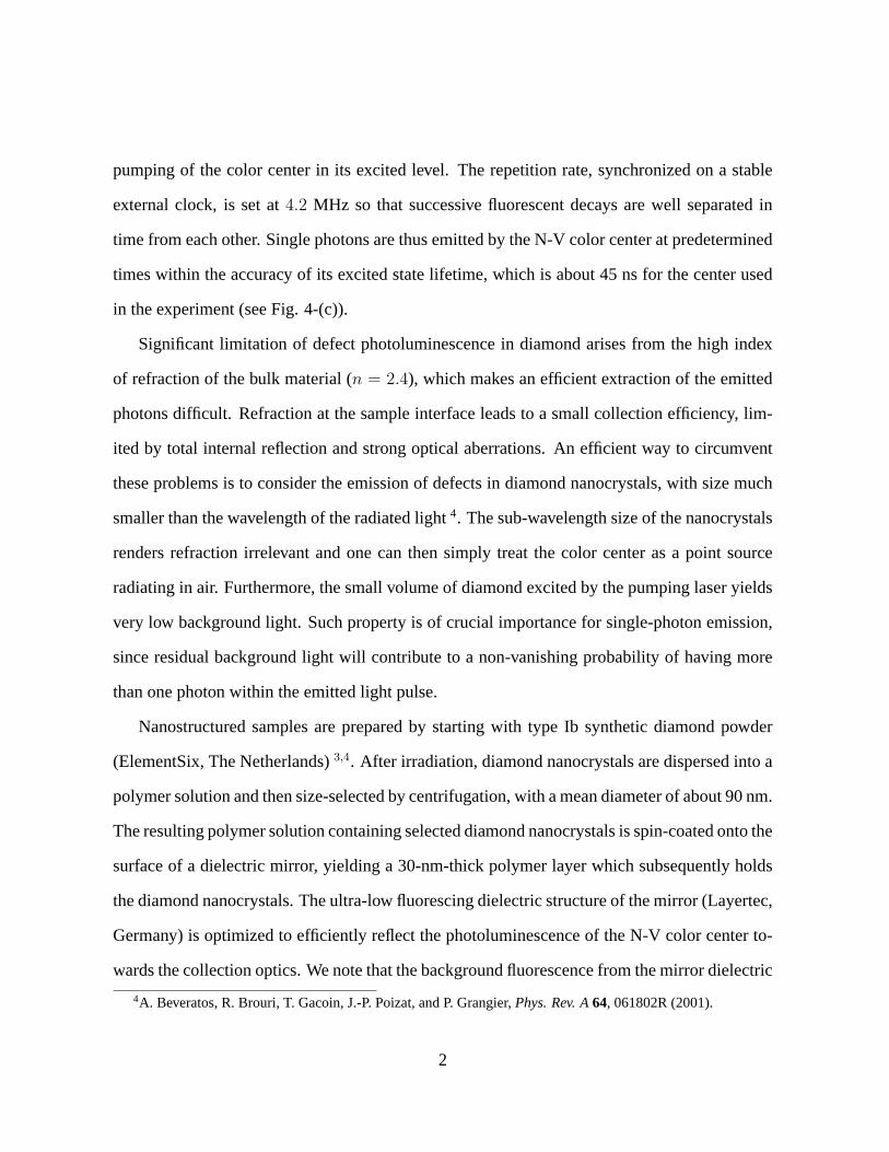
pumping of the color center in its excited level. The repetition rate, synchronized on a stable
external clock, is set at4.2 MHz so that successive fluorescent decays are well separated in
time from each other. Single photons are thus emitted by the N-V color center at predetermined
times within the accuracy of its excited state lifetime, which is about 45 ns for the center used
in the experiment (see Fig. 4-(c)).
Significant limitation of defect photoluminescence in diamond arises from the high index
of refraction of the bulk material (n = 2.4), which makes an efficient extraction of the emitted
photons difficult. Refraction at the sample interface leads to a small collection efficiency, lim-
ited by total internal reflection and strong optical aberrations. An efficient way to circumvent
these problems is to consider the emission of defects in diamond nanocrystals, with size much
smaller than the wavelength of the radiated light4. The sub-wavelength size of the nanocrystals
renders refraction irrelevant and one can then simply treat the color center as a point source
radiating in air. Furthermore, the small volume of diamond excited by the pumping laser yields
very low background light. Such property is of crucial importance for single-photon emission,
since residual background light will contribute to a non-vanishing probability of having more
than one photon within the emitted light pulse.
Nanostructured samples are prepared by starting with type Ib synthetic diamond powder
(ElementSix, The Netherlands)3,4. After irradiation, diamond nanocrystals are dispersed into a
polymer solution and then size-selected by centrifugation, with a mean diameter of about 90 nm.
The resulting polymer solution containing selected diamond nanocrystals is spin-coated onto the
surface of a dielectric mirror, yielding a 30-nm-thick polymer layer which subsequently holds
the diamond nanocrystals. The ultra-low fluorescing dielectric structure of the mirror (Layertec,
Germany) is optimized to efficiently reflect the photoluminescence of the N-V color center to-
wards the collection optics. We note that the background fluorescence from the mirror dielectric
4A. Beveratos, R. Brouri, T. Gacoin, J.-P. Poizat, and P. Grangier,Phys. Rev. A64, 061802R (2001).
2
layers is strongly reduced due to photobleaching after a few hours of sample illumination, while
the N-V color center emission properties remain unaffected.
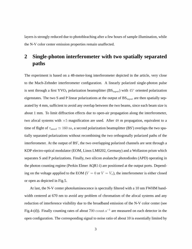
2 Single-photon interferometer with two spatially separatedpaths
The experiment is based on a 48-meter-long interferometer depicted in the article, very close
to the Mach-Zehnder interferometer configuration. A linearly polarized single-photon pulse
is sent through a first YVO4 polarization beamsplitter (BSinput) with 45◦ oriented polarization
eigenstates. The two S and P linear polarizations at the output of BSinput are then spatially sep-
arated by 4 mm, sufficient to avoid any overlap between the two beams, since each beam size is
about 1 mm. To limit diffraction effects due to open-air propagation along the interferometer,
two afocal systems with×5 magnification are used. After48 m propagation, equivalent to a
time of flight of τinterf ' 160 ns, a second polarization beamsplitter (BS′) overlaps the two spa-
tially separated polarizations without recombining the two orthogonally polarized paths of the
interferometer. At the output of BS′, the two overlapping polarized channels are sent through a
KDP electro-optical modulator (EOM, Linos LM0202, Germany) and a Wollaston prism which
separates S and P polarizations. Finally, two silicon avalanche photodiodes (APD) operating in
the photon counting regime (Perkin Elmer AQR14) are positioned at the output ports. Depend-
ing on the voltage appplied to the EOM (V = 0 or V = Vπ), the interferometer is either closed
or open as depicted in Fig.5.
At last, the N-V center photoluminescence is spectrally filtered with a 10 nm FWHM band-
width centered at 670 nm to avoid any problem of chromatism of the afocal systems and any
reduction of interference visibility due to the broadband emission of the N-V color center (see
Fig.4-(d)). Finally counting rates of about700 count.s−1 are measured on each detector in the
open configuration. The corresponding signal to noise ratio of about 10 is essentially limited by
3

darkcounts of the two APDs, on the order of60 count.s−1 for each.
3 Quantum Random Number Generator
To ensure space-like separation between the entrance of the photon into the interferometer and
the choice of the interferometer configuration, the applied voltage on the EOM is randomly
chosen in real time, using a Quantum Random Number Generator (QRNG) located at the output
of the interferometer. The random numbers are generated from the amplified shotnoise of a
white light beam. For each clock pulse, i.e. every238 ns, fast comparison of the amplified
shotnoise to the zero level generates a binary random number0 or 1.
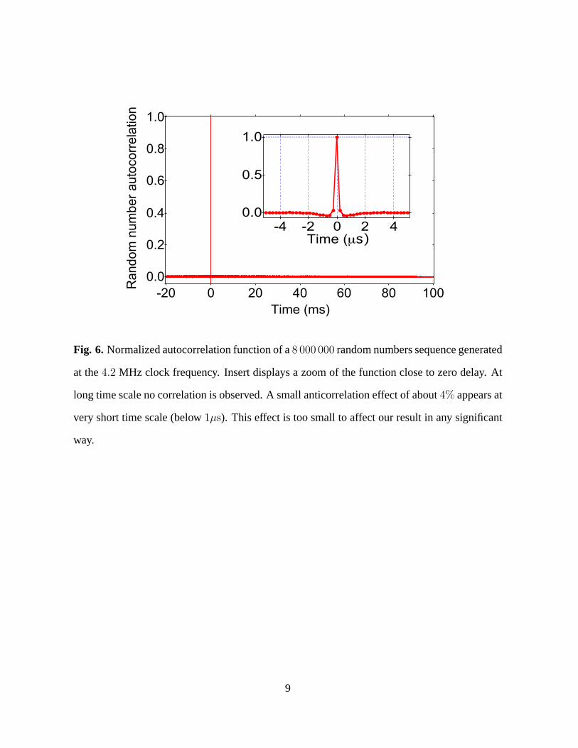
As shown on Fig. 6, the autocorrelation function of a random number sequence reveals no
significant correlations between different drafts. However, a small anticorrelation effect at short
time scale exists, presumably due to small oscillations in the amplified output of the shotnoise
limited photodetector. This effect, on the order of 4%, means that knowing one drawn random
number allows to correctly guess the next one with a 52% probability. This 2% deviation
from the ideal balanced QRNG is clearly not sufficient to explain the results obtained in our
experiment since it could only change the measured interference visibility and theα parameter
value by 2%. This is well beyond the observed margin.
Furthermore, we also checked by direct sampling of the amplified shotnoise every 10 ns that
its correlation time is approximatively 60 ns. This measurement, well below the time of flight
of the photonsτinterf , confirms that the result of the QRNG is essentially causally disconnected
from the entering of the photon into the interferometer.
4 Timing of the experiment
The color center is excited everyτrep = 238 ns by the pulsed pump laser. Since the time of
flight of the photon in the interferometerτinterf is smaller than the excitation periodτrep, at most
4

one single-photon pulse is inside the interferometer at a time. A small fraction of the pump
pulsed laser is used to clock-trigger the control and acquisition electronics located at the output
of the interferometer. This electronics are based on an FPGA programmable circuit generating
for each clock pulse the following sequence. First, fast comparison of the amplified shotnoise
to the zero level generates a binary random number 0 or 1 which drives the voltage applied
to the EOM, corresponding to the choice between the open and closed configurations. Then a
detection gate of durationτd = 40 ns is adjusted with appropriate time delays to coincide with
the photon arrival on detectors D1 and D2. This gated detection leads to a significant decrease
of the effective number of dark counts of D1 and D2.
The FPGA electronics is programmed in order that the random number generation is re-
alized 160 ns before the detection gate, which corresponds to the time of flightτinterf of the
photon inside the interferometer. The QRNG is then drawn simultaneously with the entering of
the photon into the interferometer, within the accuracy of the excited level lifetime of the N-V
centerτsp = 44.5± 0.5ns (see Fig. 4-(b)).
As shown in the space-time diagram of Fig. 7, if the single-photon appears at the very be-
ginning (resp. at the very end) of its time-emission window, it has been inside the interferometer
for 85 ns (resp. 40 ns), meaning 25 m (resp. 12 m) away from the input beamsplitter, when the
EOM voltage starts to commute. Furthermore, such timing ensures that the two events “entering
of the photon into the interferometer at BSinput” and “choice of the experimental configuration
at BSoutput” are space-like separated in the relativistic sense, as required in Wheeler’s proposal.
Indeed, as it clearly appears in Fig. 7, the photon enters the future light-cone of the random
choice when it is about at the middle of the interferometer, long after passing BSinput.
5

VN
C(c)(a)
(b)
80x10-3
60
40
20
0Nor
mal
ized
g(2
) (τ)
-200 0 200Delay τ (ns)
Interferometer
scanning mirror
dichroic mirror
filter
pulsed excitation λ=532 nm
pinhole
diamond sample
Spectrometer
(d)
measurementg(2)(!)
250
200150
10050
0
Coun
ts
850800750700650600550Wavelength (nm)
(1) (2)
Fig. 4. (a)-N-V color center consisting in a substitutional Nitrogen atom (N), associated to a Va-
cancy (V) in an adjacent lattice site of the diamond crystalline matrix.(b)- Confocal microscopy
setup. The532 nm pulsed excitation laser beam is tightly focused on a diamond nanocrystals
with a high numerical aperture (NA=0.95) microscope objective. The photoluminescence of the
N-V color center is collected by the same objective and then spectrally filtered from residual
pumping light. Following standard confocal detection scheme, the collected light is focused
onto a100 µm diameter pinhole. To identify a well isolated photoluminescent emitter, the sam-
ple is first raster scanned. For the center used in the experiment, a signal over background ratio
of about 10 is achieved.(c)-The unicity of the emitter is then ensured by observation of anti-
bunching in the second order correlation functiong(2)(τ) of the N-V center photoluminescence,
recorded by a standard Hanbury Brown and Twiss setup. The very small remaining value at
zero delayg(2)(0) = 0.12 is due to background emission from the substrate and from the dia-
6

mond sample in which the color center is embedded. Exponential fit ofg(2)(τ) (blue line) gives
the excited level lifetime of the defectτsp = 44.5 ± 0.5 ns. (d)-Part of the photoluminescence
can be also taken to record the emission spectrum of the N-V color center. The two sharp lines
(1) and (2) are respectively the two-phonon Raman scattering line of the diamond matrix as-
sociated to the excitation wavelength and the zero phonon line at 637 nm which characterizes
photoluminescence of negatively charged N-V color centers.
7
D1
D2V = 0
EOM optical axes
D1
V = V! D2
Polarization state at BS' output
Polarization state at EOM output
Polarization state at the WP output
EOMvoltage
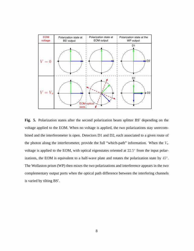
Fig. 5. Polarization states after the second polarization beam splitter BS′ depending on the
voltage applied to the EOM. When no voltage is applied, the two polarizations stay unrecom-
bined and the interferometer is open. Detectors D1 and D2, each associated to a given route of
the photon along the interferometer, provide the full “which-path” information. When theVπ
voltage is applied to the EOM, with optical eigenstates oriented at22.5◦ from the input polar-
izations, the EOM is equivalent to a half-wave plate and rotates the polarization state by45◦.
The Wollaston prism (WP) then mixes the two polarizations and interference appears in the two
complementary output ports when the optical path difference between the interfering channels
is varied by tilting BS′.
8
1.0
0.8
0.6
0.4
0.2
0.0
Ran
dom
num
ber
auto
corr
elat
ion
100806040200-20Time (ms)
1.0
0.5
0.0-4 -2 0 2 4
Time (µs)
Fig. 6. Normalized autocorrelation function of a8 000 000 random numbers sequence generated
at the4.2 MHz clock frequency. Insert displays a zoom of the function close to zero delay. At
long time scale no correlation is observed. A small anticorrelation effect of about4% appears at
very short time scale (below1µs). This effect is too small to affect our result in any significant
way.
9

200150100500Time (ns)
QRNG
single-photon entering !rep
!interf
EOM
Detection gate !d
600550500Time (ns)
Clock "n-1"
Clock "n+1"
nn-1 n+1
!sp
x
t
Time (ns)
Input
Output
Choice for photon ''n''
Clock "n"
QRNG's future light cone
450400350300250Time (ns)
Fig. 7. Timing of the “delayed-choice” experiment, represented as a space-time diagram. Clock
pulses of 5 ns duration are generated by detecting part of the pump laser beam. Due to the N-V
color center radiative lifetimeτsp, the single-photon light pulses enter the interferometer within a
time window of approximately45 ns. The control and detection electronics is based on a FPGA
programmable circuit with a few nanoseconds jitter. To account for propagation delays and
response time, the interferometer configuration applied to photon “n” is synchronised on clock
pulse “n-1” which triggers the emission of photon “n-1” (see green bented line corresponding
to speed-of-light propagation). The sequence for the measurement applied to photon “n” is
done in three steps. First, as represented in blue, the binary random number which determines
the interferometer configuration is generated by the QRNG simultaneously with the entering of
10
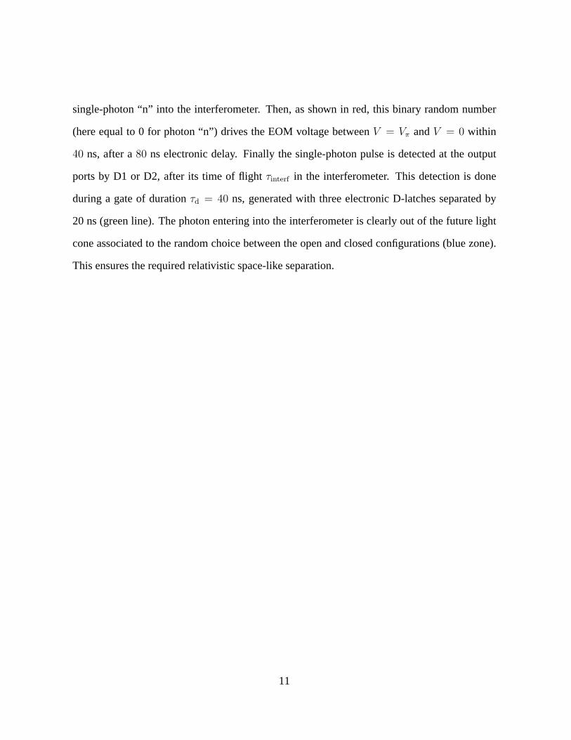
single-photon “n” into the interferometer. Then, as shown in red, this binary random number
(here equal to 0 for photon “n”) drives the EOM voltage betweenV = Vπ andV = 0 within
40 ns, after a80 ns electronic delay. Finally the single-photon pulse is detected at the output
ports by D1 or D2, after its time of flightτinterf in the interferometer. This detection is done
during a gate of durationτd = 40 ns, generated with three electronic D-latches separated by
20 ns (green line). The photon entering into the interferometer is clearly out of the future light
cone associated to the random choice between the open and closed configurations (blue zone).
This ensures the required relativistic space-like separation.
11