Supporting Information Large-Scale, Ultra-Dense and ...
8
Supporting Information Large-Scale, Ultra-Dense and Vertically Standing Zinc Phthalocyanine -Stacks as the Hole-Transporting Layer on the ITO Electrode ** Zhenhuan Lu, Chuanlang Zhan*, Xiaowei Yu, Weiwei He, Hui Jia, Lili Chen, Ailing Tang, Jianhua Huang and Jiannian Yao* Beijing National Laboratory for Molecular Science, CAS Key Laboratory of Photochemistry, Institute of Chemistry, Chinese Academy of Sciences, Beijing, 100190, P. R. China. E-mail: [email protected], [email protected]. Contents 1. General Information. ...................................................................................................................................................... 1 2. Synthetic procedure of the zinc phthalocyanine (ZnPc). ............................................................................................... 1 3. The cleaned procedure of the indium tin oxide (ITO) glass. ......................................................................................... 2 4. The prepare procedure of the amorphous ZnPc film device. ......................................................................................... 2 5. Estimations of the conductivity of the ZnPc nanorods using The Herzt’s model. ......................................................... 2 6. Estimations of the hole mobilities of the ZnPc nanorods follwing the Space charge limited currents (SCLC) semi-empirical equation measured using c-AFM. ......................................................................................................... 2 7. Fabrications and Characterizations of organic Solar Cells (OSCs). .............................................................................. 3 8. Supporting figures.......................................................................................................................................................... 4 Figure S1. ...................................................................................................................................................................... 4 Figure S2. ...................................................................................................................................................................... 4 Figure S3. ...................................................................................................................................................................... 4 Figure S4. ...................................................................................................................................................................... 5 Figure S5. ...................................................................................................................................................................... 5 Figure S6. ...................................................................................................................................................................... 5 Figure S7. ...................................................................................................................................................................... 5 Figure S8. ...................................................................................................................................................................... 7 Figure S9. ...................................................................................................................................................................... 7 Figure S10. .................................................................................................................................................................... 7 Figure S11. .................................................................................................................................................................... 7 9. Supporting table. ............................................................................................................................................................ 7 Table S1......................................................................................................................................................................... 7 References ............................................................................................................................................................................. 7 Electronic Supplementary Material (ESI) for Journal of Materials Chemistry This journal is © The Royal Society of Chemistry 2012
Transcript of Supporting Information Large-Scale, Ultra-Dense and ...
Supporting Information
Large-Scale, Ultra-Dense and Vertically Standing Zinc Phthalocyanine
-Stacks as the Hole-Transporting Layer on the ITO Electrode **
Zhenhuan Lu, Chuanlang Zhan*, Xiaowei Yu, Weiwei He, Hui Jia, Lili Chen, Ailing Tang,
Jianhua Huang and Jiannian Yao*
Beijing National Laboratory for Molecular Science, CAS Key Laboratory of Photochemistry, Institute of
Chemistry, Chinese Academy of Sciences, Beijing, 100190, P. R. China.
E-mail: [email protected], [email protected].
Contents
1. General Information. ...................................................................................................................................................... 1
2. Synthetic procedure of the zinc phthalocyanine (ZnPc). ............................................................................................... 1
3. The cleaned procedure of the indium tin oxide (ITO) glass. ......................................................................................... 2
4. The prepare procedure of the amorphous ZnPc film device. ......................................................................................... 2
5. Estimations of the conductivity of the ZnPc nanorods using The Herzt’s model. ......................................................... 2
6. Estimations of the hole mobilities of the ZnPc nanorods follwing the Space charge limited currents (SCLC)
semi-empirical equation measured using c-AFM. ......................................................................................................... 2
7. Fabrications and Characterizations of organic Solar Cells (OSCs). .............................................................................. 3
8. Supporting figures. ......................................................................................................................................................... 4
Figure S1. ...................................................................................................................................................................... 4
Figure S2. ...................................................................................................................................................................... 4
Figure S3. ...................................................................................................................................................................... 4
Figure S4. ...................................................................................................................................................................... 5
Figure S5. ...................................................................................................................................................................... 5
Figure S6. ...................................................................................................................................................................... 5
Figure S7. ...................................................................................................................................................................... 5
Figure S8. ...................................................................................................................................................................... 7
Figure S9. ...................................................................................................................................................................... 7
Figure S10. .................................................................................................................................................................... 7
Figure S11. .................................................................................................................................................................... 7
9. Supporting table. ............................................................................................................................................................ 7
Table S1. ........................................................................................................................................................................ 7
References ............................................................................................................................................................................. 7
Electronic Supplementary Material (ESI) for Journal of Materials ChemistryThis journal is © The Royal Society of Chemistry 2012

1
1. General Information.
All the chemical reagents were purchased reagent-grade from Acros or Aldrich Corporation and were used without
further purification unless otherwise stated. All solvents were purified using standard procedures. 1H and 13C NMR spectra were recorded on a Bruker AVANCE 400 using tetramethylsilane (TMS; δ = 0 ppm) as an
internal standard. Mass spectra (MALDI-TOF-MS) were determined on a Bruker BIFLEX III mass spectrometer. FT-IR
spectra were recorded on a TENSOR-27 spectrometer using KBr pellets. UV-vis absorption was recorded on a Hitachi
U-3010 spectrophotometer. XRD measurements were performed by using a X-ray powder diffraction (XRD, BRUKER
D8 Focus) with Cu Kα as the radiation source (λ = 1.5418 Å) and operated at 40 kV and 40 mA.
The SEM was recorded with a field emission scanning electron microscope (FESEM, Hitachi S-4800), operating at an
accelerating voltage of 1.5 kV. TEM measurements were performed on a JEOL JEM-2011 electron microscope,
operating at an accelerating voltage of 200 kV. The Atomic Force Microscopy (AFM) and conductive -AFM (c-AFM)
measurements were performed with Dimension Icon Atomic Force Microscope with ScanAsyst in tapping mode and
fixed point conductive atomic force microscopy Mode.
The electrochemical measurements were carried out in a solution of potassium ferricyanide (2 mM K3Fe(CN)6, 1 M
KNO3) in water with a computer-controlled Zennium electrochemical workstation. The obtained ITO, a Pt wire, and an
Ag/AgCl electrode were used as the working, counter, and reference electrodes, respectively. The electrochemical cyclic
voltammetry (CV) for characterizations of the HOMO energy level of ZnPC was performed using a Zahner IM6e
electrochemical workstation in a 0.1 mol/L tetrabutylammonium hexafluorophosphate (Bu4NPF6) dimethylformamide (DMF)
solution with a scan speed at 0.1 V/s.
X-ray photoelectron spectroscopy (XPS) data were obtained with an ESCALab220i-XL electron spectrometer from
VG Scientific using 300W AlKα radiation. The base pressure was about 3×10⁻⁹ mbar. The binding energies were
referenced to the C1s line at 284.8 eV from adventitious carbon.
2. Synthetic procedure of the zinc phthalocyanine (ZnPc).
The tetra-amino ZnPc was prepared by following the literature methods.[1] Then, tetra-amino ZnPc (0.6 g, 0.79 mmol)
was dissolved in 50mL tetrahydrofuran (THF). Under an ice-water bath, methyl 4-chloro-4-oxobutanoate (0.53 g, 3.48
mmol) and N, N-diisopropylethylamine (0.45g, 3.5 mmol) were added. After 30min, the reaction mixture was stirring at
room temperature for 30min. The solvent was removed and the residue was purified by neutral-Al2O3 column
chromatography (CH2Cl2/CH3OH=100:1). The product tetra 4-methoxy-4-oxobutanamido ZnPc was obtained (0.44 g,
0.40 mmol, yield 51%). After that, tetra 4-methoxy-4-oxobutanamido ZnPc (0.40 g, 0.37 mmol) was dissolved in a
50mL mixture of THF and MeOH (v/v=1:1). To the reaction mixture, 2% NaOH aqueous solution (1mL) was added.
The reaction mixture was stirring at 60� over night. The most solvent (40mL) was removed. The residue was acidized
by 1M HCl to pH=4, then 80mL water was added. Dark green precipitate was appeared, filtered off and washed by water
to give the final product, tetra 3-carboxypropanamido ZnPc (0.32 g, 0.31 mmol, yield 83%). 1H NMR (400MHz, DMSO,
δ(ppm)): 10.83 (d, 4H, J=12Hz, NH), 9.75 (d, 4H, J=16 Hz, ArH), 9.23(s, 4H, ArH), 8.32 (d, 4H, J=16 Hz, ArH), 2.88 (t,
8H, J=4 Hz, CH2), 2.75 (t, 8H, J=4 Hz, CH2); 13C NMR (100MHz, DMSO-d6): 174, 170, 152, 145, 141, 138, 122, 120,
112, 31, 29; IR υmax (KBr): 3547, 3337, 3075, 2951, 2865, 1711, 1678 , 1511, 1414, 1369, 1260, 1107, 662 cm-1;
MALDI-TOF MS(m/z): [M+H]+ calcd for C48H36N12O12Zn, 1037.19; found 1037.20. HR-ESI MS (m/z): [M+H] + calcd
Electronic Supplementary Material (ESI) for Journal of Materials ChemistryThis journal is © The Royal Society of Chemistry 2012
2
for C48H36N12O12Zn, 1037.19; found 1037.19. UV-Vis (DMF, 1×10⁻⁴mol/L) λmax (nm) and ε (L.mol-1.cm-1): 294
(0.285×10⁻⁵), 353 (0.657×10⁻⁵), 622 (0.369×10⁻⁵), 688(1.118×10⁻⁵).
3. The cleaned procedure of the indium tin oxide (ITO) glass.
The indium tin oxide (ITO) glass was precleaned, respectively, with deionized water, acetone and isopropanol and
treated in a Novascan PSD-ultraviolet-ozone chamber for 30 min.
4. The prepare procedure of the amorphous ZnPc film device.
An Au electrode device as show in Figure S5 was prepared by vacuum deposition of Au on a Cr coated Si substrate.
Then a 0.1 mM ZnPc solution (in MeOH) was dropwise on the device. After the solvent was completely evaporated, the
device was dried under vacuum for about 30 minutes.
5. Estimations of the conductivity of the ZnPc nanorods using the Herzt’s model.[2]
The conductivity (σ) of the nanorod is calculated using the following Eq.:
σ=IL/(VS) (1)
Where, L is the height (e.g. length) of the ZnPc nanorod and S the effective cross-sectional area of the conductive part.
The radius of the effective cross-sectional area (S, assumed to be circular), ρ, is estimated from Eq. (2) by following the
Hertz’s model (Figure 3b in the main text):
1/33
=4
F R
E
(2)
Where, F is the applied force, R the tip radius (about 20 nm according to the data provided by the manufacturer), F the
loading force applied by the AFM tip (F= setpoint (V) ×deflection sensitivity (nm/V) ×spring constant (N/m) =2V×100
nm/V×2.8 N/m=560 nN) and E* the effective elasticity modulus determined by 1/E*=1/Etip+1/EZnPc. We assume that the
elasticity modulus for the ZnPc nanorod is similar to that of the common organic polymer materials, about 2 Gpa, and
that of the mixture of MPc and polymers, about 2.5-4 Gpa (unfortunately, to the best of our knowledge, there are no
measurements of the mechanical properties for pure MPc derivatives). The Etip is relative to the metal of Pt/Ir, in the
order of 102 Gpa normally, for example, 169 GPa for Pt. Therefore, 1/E*≈1/EZnPc. According to the values of R (20 nm),
F (560 nN) and E* (herein, we select the value of 2 GPa), the contact radius of ρ is estimated as ~16 nm. This yields an
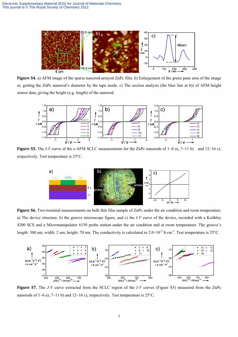
effective S value of 800 nm2. The length of the nanorod (L) is estimated from section analysis of AFM height sensor data,
as shown in Figure S4. Applying this effective S and L values to Eq. (1), the conductivity is then calculated and listed in
Table S1.
6. Estimation of the hole mobilities of the ZnPc nanorods following the Space charge limited currents (SCLC)
semi-empirical equation measured with c-AFM.[3]
1.6 0.12
3
V LJ
L d
1/ 20. 89γ( V/ L)oαεεμe δ (3)
The α in Eq. (3) is the prefactor (α=8.2), εo the permittivity of free space (εo=8.85419×10⁻¹² F/m), ε the permittivity of
ZnPc film (ε=10 F/m)[4], δ an empirical dimensionless parameter (δ=7.8), d the diameter of the tip-substrate contact
area (d=32 nm), γ expresses the apparent field dependence (or charge density dependence) of the mobility, μ the charge
Electronic Supplementary Material (ESI) for Journal of Materials ChemistryThis journal is © The Royal Society of Chemistry 2012

3
carrier mobility, V the applied voltage, J the average current density at the AFM tip, and L the lengths of the ZnPc
nanorods.
After natural logarithm processing of Eq. (3), a transformation formulacan can be got as:
1/21.4 1.6
2ln 0.89 ln
JL d V
V L
oγ αεεμδ (4)
In the case of the c-AFM, the measured I–V curve (As show in the figure above) shows ohmic behavior at low voltage
bias, with the current density varying linearly with V (blue line area), whereas at the high voltage, sudden charge
injection induces SCLC behavior with I ~ V2 (red line area).
We extract the data of the SCLC region, with
1/2V
L
for the X axis to 1.4 1.6
2ln
JL d
V
for the Y axis, drawing and
linear fit gives out a straight line. The intercept of the line is ln oαεεμδ , and then the probably value of the
mobility (μ) can be calculated (Figure S7).
7. Fabrications and Characterizations of organic Solar Cells (OSCs).
The ZnPc OSC devices were fabricated with configurations of ITO/densely nanorod-arrayed ZnPc film (av. 36
nm)/poly-(3-hexyl) thiophene (P3HT): [6, 6]-phenyl-C61-butyric acid methyl ester (PC61BM)/Ca/Al. A
1,2-dichlorobenzene solution of P3HT/PCBM (40 mg/mL) spin-coated on the surface of the densely nanorod-arrayed
ZnPc film to form a photoactive layer (ca. 200nm). Then, the Ca/Al cathode was deposited on the photoactive layer by
the vacuum evaporation (ca. 20/60 nm). The effective area of one cell is 6 mm2. The current-voltage (I-V) measurement
of the devices was conducted on a computer-controlled Keithley 2400 Source Measure Unit. A xenon lamp with AM1.5
filter was used as the white light source, and the optical power at the sample was 100 mW/cm2. EQE measurements were
carried out on an oriel IQE 200 (Newport). The conventional OSC devices were fabricated with configurations of ITO /
PEDOT: PSS/P3HT/PCBM/Ca/Al. A thin layer (ca. 30 nm) of poly (3, 4-ethylene- dioxythiophene): poly
(styrenesulfonate) (PEDOT: PSS, Baytron P VP AI 4083, Germany) was spin-coated onto the ITO glass with
spin-coating speed of 2000 rpm and baked at 150℃ for 10 min. Other steps are the same as the above mentioned.
Electronic Supplementary Material (ESI) for Journal of Materials ChemistryThis journal is © The Royal Society of Chemistry 2012
4
8. Supporting figures.
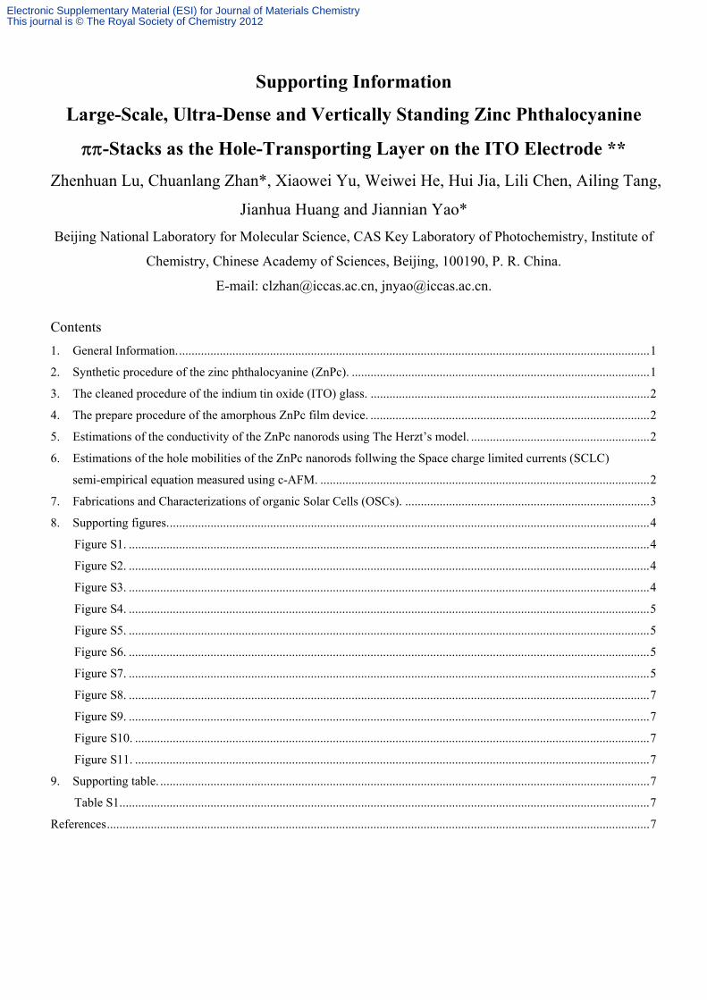
Figure S1.SEM images of a) ZnPc nanofibers randomly precipitating on the surface of the nanorod-arrays, b) after
sonication treatment for 5 seconds, showing that most of the nanofibers are removed.
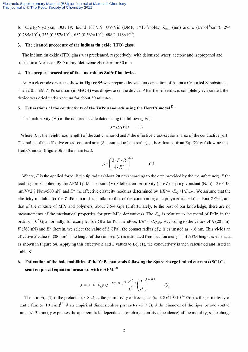
FigureS2.Cyclic voltammograms (CV) of the self-assembled single molecular layer of ZnPc on the ITO substrate after
reacting for different time from 0 h to 48 h. The CVs were carried out in an aqueous solution of potassium ferricyanide
(2 mM K3Fe(CN)6, 1 M KNO3) with a scan rate of 100mV/s.
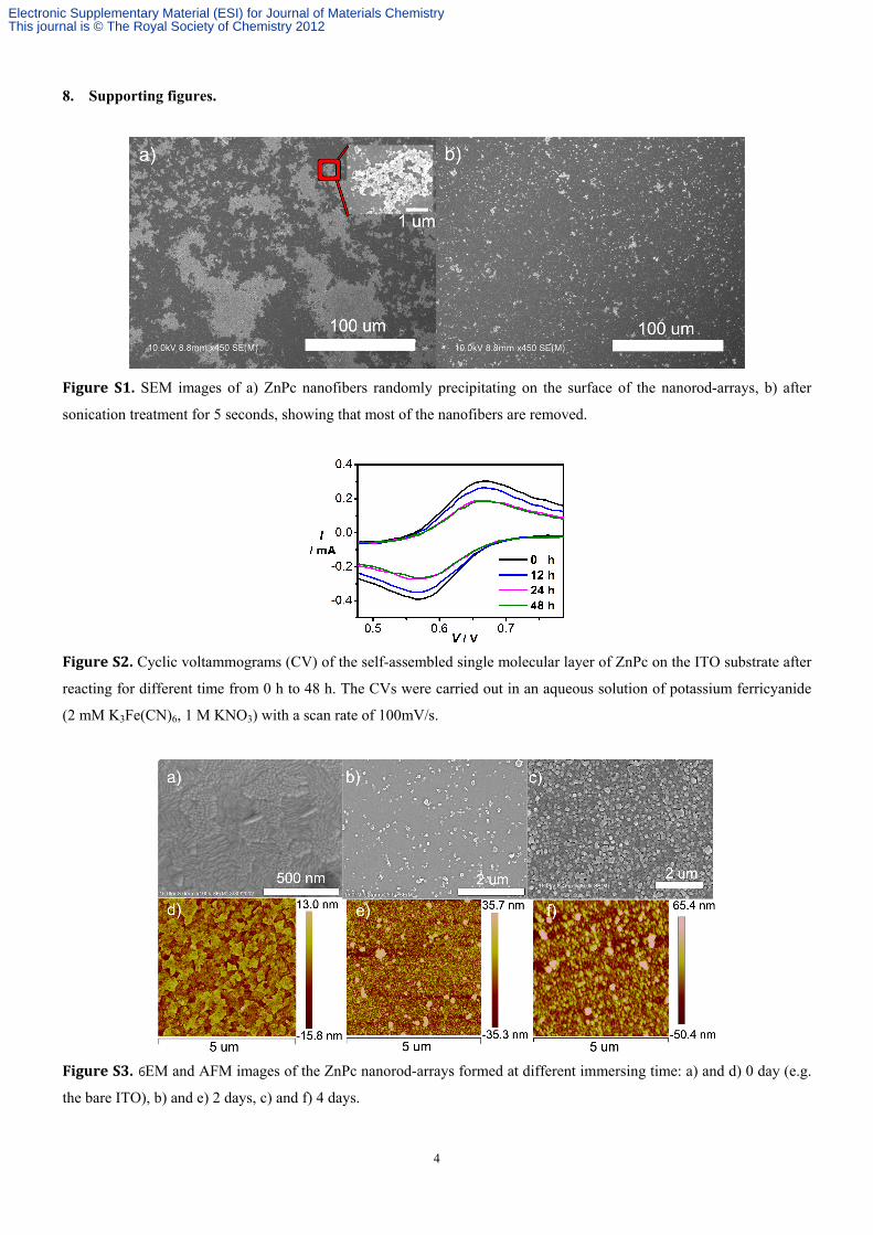
FigureS3.�EM and AFM images of the ZnPc nanorod-arrays formed at different immersing time: a) and d) 0 day (e.g.
the bare ITO), b) and e) 2 days, c) and f) 4 days.
Electronic Supplementary Material (ESI) for Journal of Materials ChemistryThis journal is © The Royal Society of Chemistry 2012
5
FigureS4.a) AFM image of the sparse nanorod-arrayed ZnPc film. b) Enlargement of the green pane area of the image
a), getting the ZnPc nanorod’s diameter by the tape mode. c) The section analysis (the blue line at b)) of AFM height
sensor data, giving the height (e.g. length) of the nanorod.
FigureS5.The I-V curve of the c-AFM SCLC measurements for the ZnPc nanorods of 1~6 a), 7~11 b) and 12~16 c),
respectively. Test temperature is 25C.
FigureS6.Two-terminal measurements on bulk thin film sample of ZnPc under the air condition and room temperature.
a) The device structure, b) the groove microscope figure, and c) the I-V curve of the device, recorded with a Keithley
4200 SCS and a Micromanipulator 6150 probe station under the air condition and at room temperature. The groove’s
length: 300 um, width: 2 um, height: 70 nm. The conductivity is calculated to 2.0×10⁻⁵ Scm-1. Test temperature is 25C.
Figure S7. The J-V curve extracted from the SCLC region of the I-V curves (Figure S5) measured from the ZnPc
nanorods of 1~6 a), 7~11 b) and 12~16 c), respectively. Test temperature is 25C.
Electronic Supplementary Material (ESI) for Journal of Materials ChemistryThis journal is © The Royal Society of Chemistry 2012

6
0 2 4 6 8 10 12
0.00
0.01
0.02
0.03
0.04
0.05
I / A
V / V
FigureS8.The typical I-V curve of the amorphous ZnPc film (av. 1000 nm) measured using SCLC method with the
device configuration of ITO/PEDOT:PSS/the amorphous ZnPc film / Au (60 nm). Such a curve does not show any SCLC
regions within the experimental voltage range, thus we can not get the hole mobility of the amorphous ZnPc film.
-2 -1 0 1 2
-2
0
2
4
6
I 10
-5 /
A
V / V
HOMO: -(0.82+4.40)=-5.22 eVLUMO: 1240/715-5.22=-3.48 eV
-0.82 V
300 400 500 600 700 800
0.0
0.5
1.0
/ nm
Ab
s (
a.u
.)
715 nm
FigureS9.The CV of ZnPc in the 0.1 M Bu4NPF6 DMF solution at 0.1 V/s, with Ag/AgCl as the reference electrode (Left).
Noted that the LUMO energy level was estimated from the absorption spectrum, in which the off-set in the long-wavelength
side is about 715 nm (Right).
FigureS10.The J-V curve of a typical OSC with the configuration of ITO/the amorphous ZnPc film (av. 40 nm)/ P3HT:
PC61BM (200 nm)/Ca (20 nm)/Al (60 nm).
Electronic Supplementary Material (ESI) for Journal of Materials ChemistryThis journal is © The Royal Society of Chemistry 2012

7
FigureS11.a) A typical AFM image of the 8 nm thick nanorod-arrayed ZnPc film on the ITO substarte, showing the
unmatured deposition of the thinner film and rough surface. b) A typical SEM image of the 60 nm thick, densely
nanorod-arrayed ZnPc film, showing the un-removed, disordered ZnPc nanofibers randomly precipitating on the surface.
9. Supporting table.
Table S1. The data of the 16 ZnPc nanorods determined by c-AFM measure
No. Height
[nm]
Diameter
[nm]
[S·cm-1]
μ
[cm2·V-1·s-1]
1 32.7 41.2 0.00059 0.0045 2 54.3 62.1 0.0012 0.0064 3 75.0 78.1 0.0019 0.0075 4 32.7 51.6 0.00096 0.0019 5 46.0 39.5 0.0014 0.0029 6 35.4 52.7 0.0012 0.0013 7 29.8 41.5 0.00066 0.0029 8 29.8 54.5 0.00073 0.0020 9 44.6 59.9 0.0012 0.0044
10 26.8 40.5 0.00076 0.0016 11 30.1 39.4 0.00091 0.0014 12 38.9 44.6 0.00079 0.0052 13 35.9 52.3 0.00091 0.0032 14 32.7 41.5 0.00077 0.0031 15 21.2 42.8 0.00059 0.0012 16 51.7 69.0 0.0013 0.0050
*Test temperature is 25℃
Reference
[1] W. Duan, Z. Wang, M. J. Cook, J. Porphyr. Phthalocya 2009, 13, 1255-1261. [2] L. Welte, A. Calzolari, R. Di Felice, F. Zamora, J. Gomez-Herrero, Nat. Nanotechnol. 2010, 5, 110-115. [3] O. G. Reid, K. Munechika, D. S. Ginger, Nano Lett. 2008, 8, 1602-1609. [4] H. M. Zeyada, M. M. El-Nahass, Appl. Surf. Sci. 2008, 254, 1852-1858.
Electronic Supplementary Material (ESI) for Journal of Materials ChemistryThis journal is © The Royal Society of Chemistry 2012