study of magnetism in dilute magnetic semiconductors based on iii-v nitrides a dissertation
121
STUDY OF MAGNETISM IN DILUTE MAGNETIC SEMICONDUCTORS BASED ON III-V NITRIDES A DISSERTATION SUBMITTED TO THE DEPARTMENT OF MATERIALS SCIENCE AND ENGINEERING AND THE COMMITTEE ON GRADUATE STUDIES OF STANFORD UNIVERSITY IN PARTIAL FULFILLMENT OF THE REQUIREMENTS FOR THE DEGREE OF DOCTOR OF PHILOSOPHY Rekha Rajaram March 2007
Transcript of study of magnetism in dilute magnetic semiconductors based on iii-v nitrides a dissertation
STUDY OF MAGNETISM IN DILUTE MAGNETIC
SEMICONDUCTORS
BASED ON III-V NITRIDES
A DISSERTATION
SUBMITTED TO THE DEPARTMENT OF MATERIALS
SCIENCE AND ENGINEERING
AND THE COMMITTEE ON GRADUATE STUDIES
OF STANFORD UNIVERSITY
IN PARTIAL FULFILLMENT OF THE REQUIREMENTS
FOR THE DEGREE OF
DOCTOR OF PHILOSOPHY
Rekha Rajaram
March 2007

c© Copyright by Rekha Rajaram 2007
All Rights Reserved
ii

I certify that I have read this dissertation and that, in my opinion, it
is fully adequate in scope and quality as a dissertation for the degree
of Doctor of Philosophy.
James S. Harris, Jr.
Electrical Engineering Principal Co-Advisor
I certify that I have read this dissertation and that, in my opinion, it
is fully adequate in scope and quality as a dissertation for the degree
of Doctor of Philosophy.
Stuart S. P. Parkin
Applied Physics Principal Co-Advisor
I certify that I have read this dissertation and that, in my opinion, it
is fully adequate in scope and quality as a dissertation for the degree
of Doctor of Philosophy.
Bruce Clemens
Materials Science and Engineering
Approved for the University Committee on Graduate Studies.
iii

iv

Abstract
Spin based electronics, commonly referred to as “spintronics”, seeks to expand the
functionalities of microelectronic devices by introducing the ability to manipulate the
carrier’s spin, in addition to or instead of its charge. Key steps in spintronic devices
include the injection, manipulation and detection of the carrier’s spin. Metal-based
spintronic devices such as spin valves have already found applications in high capacity
hard disk drive read heads and have potential in non-volatile solid state memories.
However, in order to realize the full potential of spintronics, spin manipulation must
be introduced into semiconductor devices. This in turn, requires the development of
magnetic semiconductors.
Dilute magnetic semiconductors (DMS) are a class of magnetic semiconductors in
which a fraction of the cations are substitutionally replaced by magnetic ions. The
exchange interaction between the spin of the dopant atoms and the carriers in the
semiconductor host is expected to bring about global ferromagnetic order in the entire
lattice in these materials. The search for novel DMS candidates has been driven by
two cardinal requirements - a material system with well-developed growth technology,
and a high Curie temperature.
In this work, we have investigated the growth and characteristics of one such
promising candidate, transition-metal doped InN. InN films were deposited on c-
sapphire substrates by molecular beam epitaxy, employing GaN underlayers to reduce
the lattice mismatch between the film and substrate. The films were doped from
v

0.1-6% Cr with no noticeable trace of crystalline secondary phases detected by X-
ray diffraction. However, Mn-doping led to segregation of manganese nitride. Hall
effect measurements revealed n-type behavior in both undoped as well as Cr-doped
films. A magnetic hysteresis, with a small remanence and coercivity was observed
in Cr:InN up to room temperature, confirming long-range magnetic order in this
material. X-ray magnetic circular dichroism experiments revealed dichroism at the
Cr L-edge, indicating that the Cr in the matrix was magnetically active. However,
deeper probing of the magnetic behavior revealed some metastable characteristics.
The origin of magnetic behavior in Cr:InN is discussed in the context the role of
impurity bands in mediating magnetic order.
vi

Acknowledgements
Much of the work presented in this thesis would never have materialized but for the
support, advice and companionship that I got from so many people, both in my
professional, as well as my personal life. This thesis is incomplete without a mention
of all those who have affected my graduate life in so many ways.
First and foremost, I thank my adviser, Professor James Harris whom we all have
come to know as Coach! True to his name, he has always been encouraging, providing
me with all the guidance that I needed, while at the same time allowing me enough
leeway to pursue my research interests. I am just as grateful to my co-adviser, Dr.
Stuart Parkin, who despite his busy schedule, always found the time to guide me
through difficult stints during my research career.
I thank my oral thesis committee members, professors Bruce Clemens, Anders
Nilsson and Paul McIntyre. In addition, I thank Professor Clemens for serving on my
reading committee as well.
The role played by Andreas Ney in shaping this project is invaluable, and I am
grateful for all that I learnt from him about magnetism. I thank Robin Farrow and
Ron Marks at IBM Almaden Research Center for their help with getting me oriented
with the MBE system. Valuable contributions were made by Andrew Kellock and
Vaughn Deline at IBM, who helped with RBS and SIMS measurements respectively.
I am also grateful to Elke Arenholz at the Advanced Light Source in Lawrence Berke-
ley lab as well as Mahesh Samant at IBM for their help with the X-Ray magnetic
vii

dichroism experiments. Glenn Solomon and David Miller made an instrumental con-
tribution by providing the GaN templates used in this work. I would also like to
recognize the contributions of fellow Harris group members Hyunsoo-Yang and Hopil
Bae with Hall measurements, and Photoluminescence measurements respectively.
Several people made my graduate life at Stanford a great experience. I thank my
co-workers at IBM - Brian, Kevin, Guenole, Roger, Rai, Bob, Victor and others who
were a pleasure to work with. I also enjoyed the companionship of other current and
ex Parkin group members at IBM, including Masa, Xin, Bastiaan, Nicolas, See-Hun,
Christian and Alex. I wish the newer students in the group, Cheng-Han, Li and Justin
the very best in their graduate careers. I am also thankful to all the Harris group
members for all the help and companionship that I received from them. I learnt a
lot about MBE from several students in the group including Homan, Seth, Mark and
Xiao-Jun, to name a few.
On a more personal note, the support that I have received from my friends and
family over the years is of immense value to me, and has helped me get this far. I
thank my parents and sisters for always standing by me. I am also grateful to my
in-laws for their support and acceptance of me. Finally, I thank my husband for
always believing in me.
viii

Contents
Abstract v
Acknowledgements vii
1 Introduction 1
2 Dilute Magnetic Semiconductors 6
2.1 Introduction . . . . . . . . . . . . . . . . . . . . . . . . . . . . . . . . 6
2.2 Magnetic interactions in solids . . . . . . . . . . . . . . . . . . . . . . 8
2.3 Models describing magnetism in DMS . . . . . . . . . . . . . . . . . . 10
2.3.1 Mean Field Theory . . . . . . . . . . . . . . . . . . . . . . . . 11
2.3.2 Bound Magnetic Polaron . . . . . . . . . . . . . . . . . . . . . 12
2.4 Spin glasses . . . . . . . . . . . . . . . . . . . . . . . . . . . . . . . . 15
2.5 Promising DMS candidates . . . . . . . . . . . . . . . . . . . . . . . . 17
3 Growth of InN and doped InN by MBE 20
3.1 Growth of III-Nitrides . . . . . . . . . . . . . . . . . . . . . . . . . . 21
3.2 Molecular Beam epitaxy . . . . . . . . . . . . . . . . . . . . . . . . . 23
3.2.1 Growth of InN by MBE . . . . . . . . . . . . . . . . . . . . . 25
3.2.2 Reflection High Energy Electron Diffraction (RHEED) . . . . 26
3.3 Growth of Cr and Mn-doped InN . . . . . . . . . . . . . . . . . . . . 28
ix

3.3.1 Nitridization of Sapphire . . . . . . . . . . . . . . . . . . . . . 30
3.3.2 Growth of InN and Cr, Mn-doped InN over GaN templates . . 32
4 Structural Characterization 36
4.1 Transmission Electron Microscopy . . . . . . . . . . . . . . . . . . . . 37
4.2 X-Ray Diffraction . . . . . . . . . . . . . . . . . . . . . . . . . . . . . 37
4.3 d-spacing . . . . . . . . . . . . . . . . . . . . . . . . . . . . . . . . . 42
4.4 Photoluminescence . . . . . . . . . . . . . . . . . . . . . . . . . . . . 47
4.5 Hall Effect Measurement . . . . . . . . . . . . . . . . . . . . . . . . . 50
4.5.1 Hall Effect measurements on InN and Cr:InN . . . . . . . . . 51
5 Magnetic and Electrical Characterization 54
5.1 Magnetic Characterization . . . . . . . . . . . . . . . . . . . . . . . . 54
5.2 Magnetic behavior of Cr and Mn-doped InN . . . . . . . . . . . . . . 57
5.3 Normalized saturation magnetization moment . . . . . . . . . . . . . 61
5.4 Spin-Glass like Behavior . . . . . . . . . . . . . . . . . . . . . . . . . 66
5.4.1 Measurement Procedure . . . . . . . . . . . . . . . . . . . . . 66
5.4.2 FC/ZFC measurements in Cr-doped InN . . . . . . . . . . . . 67
5.5 Metastable behavior . . . . . . . . . . . . . . . . . . . . . . . . . . . 67
5.6 Evidence of spin polarized carriers . . . . . . . . . . . . . . . . . . . . 73
6 Secondary Phases and Cr L-Edge Spectroscopy 78
6.1 Potential secondary phase - CrN . . . . . . . . . . . . . . . . . . . . . 79
6.1.1 Growth and structure . . . . . . . . . . . . . . . . . . . . . . . 79
6.1.2 Magnetic properties of CrN . . . . . . . . . . . . . . . . . . . 81
6.2 X-Ray Absorption Spectroscopy . . . . . . . . . . . . . . . . . . . . . 85
6.3 X-Ray Magnetic Circular Dichroism . . . . . . . . . . . . . . . . . . . 88
7 Conclusions 96
x

Bibliography 99
xi
List of Tables
2.1 High temperature ferromagnetism in n-type DMS [19] . . . . . . . . . 18
3.1 lattice mismatch between sapphire and III-V nitrides . . . . . . . . . 21
3.2 SIMS profile of Cr:InN films used to determine composition . . . . . . 35
4.1 Hall effect measurement on InN and Cr:InN films . . . . . . . . . . . 52
xii

List of Figures
1.1 Schematic of Datta-Das transistor . . . . . . . . . . . . . . . . . . . . 3
1.2 Curie temperatures of various DMS candidates [9] . . . . . . . . . . . 4
2.1 Semiconductor host doped with magnetic ions . . . . . . . . . . . . . 7
2.2 Representation of Polaron pair model indicating an interstitial region 14
2.3 Representation of Magnetic Polarons in a semiconductor lattice [19] . 15
2.4 Cusp observed in the magnetic susceptibility vs. temperature plot in
Au:Fe alloys with 1-2% Fe [20]. Data for 1 % Fe from Lutes and Schmit
(1964) are also included. . . . . . . . . . . . . . . . . . . . . . . . . . 16
2.5 Important characteristics of spin glasses include frustration and quenched
disorder . . . . . . . . . . . . . . . . . . . . . . . . . . . . . . . . . . 17
3.1 The preferred orientation of deposition of GaN over sapphire [44] . . 22
3.2 Schematic of Nitride MBE system . . . . . . . . . . . . . . . . . . . 24
3.3 Schematic of RHEED measurement geometry . . . . . . . . . . . . . 27
3.4 Chemistry of nitridization of sapphire [46] . . . . . . . . . . . . . . . 30
3.5 RHEED construction during sapphire nitridization (a) [1120] direction
of Sapphire (b) Polycrystalline InN deposited over the substrate . . . 31
3.6 RHEED construction during deposition (a) InN buffer layer (b) Buffer
annealed at 450◦C under N flux (c) Cr-doped InN . . . . . . . . . . . 33
3.7 SIMS profile of a 5.25% Cr-doped InN film . . . . . . . . . . . . . . . 34
xiii

4.1 TEM of a 100 nm thick InN buffer layer. (a) Shows the bright field
image (b) shows the CBED pattern obtained along the InN film . . . 37
4.2 X-Ray Diffraction . . . . . . . . . . . . . . . . . . . . . . . . . . . . . 39
4.3 High Resolution X-Ray Diffraction of Cr- and Mn-doped InN . . . . . 40
4.4 X-Ray Diffraction of Asymmetric peaks of InN . . . . . . . . . . . . . 41
4.5 X-Ray Diffraction using an area detector . . . . . . . . . . . . . . . . 43
4.6 Out-of-plane d-spacing dependence on concentration . . . . . . . . . . 44
4.7 Variation of in-plane lattice parameter (open squares) and out-of-plane
lattice parameter (circles) with Cr-doping . . . . . . . . . . . . . . . 45
4.8 Schematic of Photoluminescence in a direct band gap material . . . . 46
4.9 Photoluminescence observed in Cr-doped InN . . . . . . . . . . . . . 49
4.10 Hall Setup . . . . . . . . . . . . . . . . . . . . . . . . . . . . . . . . . 51
5.1 Schematic of the Josephson junction . . . . . . . . . . . . . . . . . . 55
5.2 Typical magnetic hysteresis of ferromagnetic materials . . . . . . . . 56
5.3 Magnetic behavior of 0.9% Cr-doped InN. (a)Shows magnetic hystere-
sis observed at various temperatures. (b) Shows the low field behavior 58
5.4 Magnetic remanence of doped InN. (a) Cr:InN shows steady decrease
in MR with temperature. (b) Mn:InN shows paramagnetic remanence
behavior . . . . . . . . . . . . . . . . . . . . . . . . . . . . . . . . . . 60
5.5 Small anisotropy observed in 1.8% Cr-doped InN. In-plane easy axis
(open squares) and out of plane hard axis (circles) . . . . . . . . . . 61
5.6 Doping level dependence of normalized saturation magnetization in
Cr:InN . . . . . . . . . . . . . . . . . . . . . . . . . . . . . . . . . . . 62
5.7 Doping level dependence of normalized saturation magnetization in
Cr:InN . . . . . . . . . . . . . . . . . . . . . . . . . . . . . . . . . . . 64
xiv
5.8 A comparison of the magnetic hysteresis obtained at 20 K from a 0.9%
Cr:InN(open circles) film with that of a 5.5% Cr:InN (squares) film . 65
5.9 Field cooled vs. Zero field cooled measurements. . . . . . . . . . . . . 66
5.10 Field cooled vs. Zero field cooled measurements in a 0.9% Cr-doped
InN. . . . . . . . . . . . . . . . . . . . . . . . . . . . . . . . . . . . . 68
5.11 Remanence dependence on temperature in 0.9% Cr-doped InN. In-
crease in remanence due to application of magnetic field observed. . . 69
5.12 Temperature dependence of ∆MR in 0.9% Cr:InN . . . . . . . . . . . 71
5.13 Remanence stays constant with time in 0.9% Cr-doped InN. . . . . . 72
5.14 Schematic of the Physical Property Measurement System (PPMS) :
Courtesy Quantum Design . . . . . . . . . . . . . . . . . . . . . . . 74
5.15 Small anomalous Hall contribution observed in a 1.8% Cr-doped InN
film, in addition to a normal Hall effect and a positive magnetoresistance. 76
5.16 Comparison between anomalous Hall contribution (open squares) of a
1.8 % Cr-doped InN film and its in plane (triangles) and out of plane
(circles) magnetization measurement. . . . . . . . . . . . . . . . . . . 77
6.1 XRD 2θ-ω patterns obtained from CrN films grown over (a) sapphire
and (b)(001) MgO. The insets show the RHEED patterns recorded
during the deposition. . . . . . . . . . . . . . . . . . . . . . . . . . . 80
6.2 Magnetic behavior of CrN films. (a) CrN deposited over sapphire shows
a small hysteresis (b) CrN deposited over MgO shows no hysteresis. . 83
6.3 Comparison of the hysteretic behavior of CrN/sapphire with that of
CrN/MgO . . . . . . . . . . . . . . . . . . . . . . . . . . . . . . . . . 84
xv

6.4 Field cooled vs. Zero field cooled behavior of CrN films. FC measure-
ment was made by cooling under 50 kOe, followed by a warm up at 100
Oe, and ZFC measurement involved cool down under zero field followed
by warm up at 100 Oe. (a) CrN deposited over sapphire shows spin
glass like behavior (b) CrN deposited over MgO shows paramagnetic
behavior . . . . . . . . . . . . . . . . . . . . . . . . . . . . . . . . . . 86
6.5 Schematic of X-Ray Absorption process . . . . . . . . . . . . . . . . 87
6.6 Cr L-edge observed in Cr:InN and in CrN . . . . . . . . . . . . . . . 88
6.7 Schematic of the physics behind the XMCD effect . . . . . . . . . . . 89
6.8 XMCD measurement setup . . . . . . . . . . . . . . . . . . . . . . . . 91
6.9 Dichroism at the Cr L-edge in Cr-doped InN . . . . . . . . . . . . . . 92
6.10 Temperature dependence of dichroism observed at the Cr L-edge in
Cr-doped InN. The spectrum taken at 100 K has been smoothed out. 94
xvi

Chapter 1
Introduction
Over the past few decades, the microelectronics industry has made tremendous progress,
with its basic unit, the integrated circuit chip infiltrating down to a large number of
everyday applications. The smallest electronic component of such a chip is the tran-
sistor, which was developed in the late 1940s by scientists at Bell labs. Over time,
the metal oxide semiconductor field effect transistor (MOSFET) evolved as the most
widely used transistor structure. In 1965 Gordon Moore, then at Fairchild Semicon-
ductor, proposed what has now come to be known as Moore’s law [1]. The essence of
the law was that the number of transistors built on a wafer would double every two
years, and that this scaling would be the key improving performance and profitability
in the microelectronic industry. However, with scaling come problems such as the
need for very thin gate oxide layers, that could be leaky and require constant re-
freshing. This would call for unacceptably high power consumption, which could act
as an impediment to further scaling down. Thus newer approaches have constantly
been explored in order to further the miniaturization of microelectronics. One such
possibility is to utilize the spin of the charge carriers in addition to their charge in
devices. There are two potential advantages of doing this, the first being the ability
of magnetic materials to remember their spin state, without any refresh. This could
1

2 CHAPTER 1. INTRODUCTION
allow us to integrate logic and storage processes and potentially lead to “instant-on”
computers, where no boot up is required. The other advantage is that relatively low
energy is required to manipulate the orientation of spin of a carrier, which could allow
development of low power spintronic devices.
Metal-based spintronics already has several applications such as hard disk drives
and read-write heads. However, new functionalities can be derived from semiconduc-
tor spintronic devices. The “Datta-Das” spin modulator [2] demonstrates an example
of such a functionality. Shown in figure 1.1is a schematic of this device. A ferromag-
netic source and drain is used in this structure, which is operated under external
magnetic field. The carriers injected into the channel are spin polarized, and readily
accepted by the drain, leading to the ‘on’ state. If, however, a small gate bias is ap-
plied, the spins start to precess or rotate, due to interaction with the semiconductor
lattice under a bias. By the time they reach the gate, their spin is no longer aligned
in the original configuration, and the drain no longer accepts them (the ’off’state).
The utility of this device lies in the fact that a very small energy is needed to precess
spins compared to that required in a MOSFET, where the channel needs to be under
inversion.
The key elements of spintronics are injection, manipulation, transfer and detec-
tion of spin-polarized carriers across a semiconductor device. A ferromagnetic source
material is required to produce such spin-polarized carriers. Ferromagnetic materials
have an unequal density of states (DOS) of spin-up and spin-down states at the Fermi
level. The degree of polarization, P can be defined as :
P = (n↓−n↑)(n↓+n↑)
(1.1)

3
Figure 1.1: Schematic of Datta-Das transistor
Where, n↓ and n↑ represent the DOS of electrons polarized in opposite directions.
Although ferromagnetic metals offer a high degree of polarization, they are inefficient
sources of spin-polarized carriers into a device. This is a result of the mismatch in
conductivity between a metal and a semiconductor [3]. This problem can be circum-
vented with the use of a magnetic semiconductor source instead. Several magnetic
semiconductors such as Europium and Chromium chalcogenides (EuS, EuO, CdCr2S4,
CdCr2Se4) [4] have been studied in the past for the interplay between semiconducting
and magnetic properties. However, these compounds are not useful technologically
due to difficult growth processes and incompatibility with systems currently in use,
such as Si or GaAs.
A class of materials known as dilute magnetic semiconductors (DMS)was devel-
oped and studied in the 1980s. The underlying principle behind ferromagnetism
in these materials was the interaction between the itinerant electrons in the semi-
conductor and the atomic magnetic moments of the dopants via an exchange bias
mechanism which resulted in spin-polarized carriers in the semiconductor. Thus one

4 CHAPTER 1. INTRODUCTION
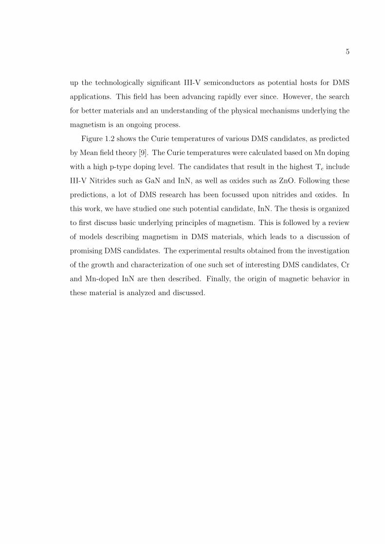
Figure 1.2: Curie temperatures of various DMS candidates [9]
could develop an all-semiconductor spintronic device with minimal losses during spin
injection. Another important aspect of DMS is that since ferromagnetism is related
to the carriers in the semiconductor, one can, in principle, deplete the semiconductor
of carriers and thus disturb ferromagnetic order. This gives rise to new possibili-
ties such as optical manipulation of magnetic behavior of DMS [6] or gate-controlled
ferromagnetism [5].
The behavior of spins in a semiconductor lattice was studied as early as the 1960s
in chalcogenides such as EuO and EuSe [7]. However, it was not until the 1980s, when
II-VI compounds such as ZnS were doped with transition metals, that the early work
on DMS started. Tremendous progress was made in the understanding of exchange
interactions between magnetic moments of the dopants and the charge carriers in the
host. However, problems with controlling the n or p-type doping of these materials,
as well as a low Curie temperature served as impediments in the development of II-VI
DMS. Nevertheless, this was a precedent to research into III-V materials as potential
DMS candidates. Initial work by Ohno and Munekata [8] on Mn doped InAs opened
5
up the technologically significant III-V semiconductors as potential hosts for DMS
applications. This field has been advancing rapidly ever since. However, the search
for better materials and an understanding of the physical mechanisms underlying the
magnetism is an ongoing process.
Figure 1.2 shows the Curie temperatures of various DMS candidates, as predicted
by Mean field theory [9]. The Curie temperatures were calculated based on Mn doping
with a high p-type doping level. The candidates that result in the highest Tc include
III-V Nitrides such as GaN and InN, as well as oxides such as ZnO. Following these
predictions, a lot of DMS research has been focussed upon nitrides and oxides. In
this work, we have studied one such potential candidate, InN. The thesis is organized
to first discuss basic underlying principles of magnetism. This is followed by a review
of models describing magnetism in DMS materials, which leads to a discussion of
promising DMS candidates. The experimental results obtained from the investigation
of the growth and characterization of one such set of interesting DMS candidates, Cr
and Mn-doped InN are then described. Finally, the origin of magnetic behavior in
these material is analyzed and discussed.

Chapter 2
Dilute Magnetic Semiconductors
2.1 Introduction
Dilute magnetic semiconductors (DMS) are semiconductors where a fraction of the
cations in the lattice are replaced substitutionally by magnetic ions (fig 2.1). The
atomic spin on these magnetic dopants is expected to interact with the carriers in
the lattice to bring about global ferromagnetic order in the material. They have
unusual magnetic characteristics due to the presence of isolated magnetic ions in
semiconducting lattice.
Significant effort was made in trying to develop various DMS candidates as well as
in understanding the origin of magnetism in these materials starting from the 1980’s.
Initial studies focused on II-VI compounds such as CdSe doped with transition metals
[12]. DMS were interesting from both a theoretical, as well as a technological stand-
point. Unlike metals, semiconductors allow properties such as band gap and carrier
concentration to be tailored to fit the application. Further, if the magnetism in the
material is related to the carrier concentration, then it might be possible to electri-
cally tune the magnetism. This could lead to a new functionality of gate-controlled
ferromagnetism. Although physics of the magnetism was thoroughly investigated in
6

2.1. INTRODUCTION 7
II-VI DMS, they were not suitable for technological applications. One of the reasons
for this was that they did not have a mature growth technology. Furthermore, fer-
romagnetic order could not be achieved at high temperatures in these materials. In
fact, the magnetism observed was attributed to spin-glass like frustrated behavior,
with very low spin glass transition temperatures.
Figure 2.1: Semiconductor host doped with magnetic ions
The area of DMS caught the attention of a much larger research community with
the demonstration of magnetic order in Mn-doped InAs [8] and GaAs [13]. Moreover,
several curious effects arise from combining magnetism with semiconductors. For
instance, in certain systems such as Co-doped TiO2 [15] or SnO2 [16] as well as in
the case of Gd-doped GaN [14], unusually large magnetic moments per dopant ion
have been observed. In order to utilize DMS for technological applications, a sound
understanding of the origin of magnetism in these materials is required. Magnetic
interactions in solids are discussed in this chapter, as well as the important models
used to predict Curie temperatures in prospective DMS candidates.

8 CHAPTER 2. DILUTE MAGNETIC SEMICONDUCTORS
2.2 Magnetic interactions in solids
The fundamental property of an electron which gives rise to its magnetic properties is
its spin. No two electrons with the same spin can occupy the same energy state. This
determines the orientation of spins of electrons in the various energy states, and is
also responsible for properties such as polarization-dependent optical selection rules.
Although spin is a quantum-mechanical property, it can be understood via a semi-
classical approach in terms of an electron orbiting along a circular orbit. With charge
e, and an angular momentum L the electron would classically induce a magnetic
dipole given by
M = current x area = Le2m0
(2.1)
If the angular momentum is presumed to be quantized in units of h then the unit
of magnetic moment is
µB = eh2m0
(2.2)
Electronic spin angular momentum only contributes in part to the total magnetic
moment of an atom. In addition, electrons around the atom also have orbital angular
momentum associated with them. The interaction of the spins on the different elec-
trons as well as their coupling with the angular momentum plays an important role
in determining whether the spins on individual electrons have any form of collective
order. Furthermore, application of an external magnetic field also contributes to the
magnetic moment of the atom by changing the orbital momentum [17] and resulting
in a diamagnetic moment.
2.2. MAGNETIC INTERACTIONS IN SOLIDS 9
Diamagnetic behavior is exhibited by all materials to some extent. When an exter-
nal magnetic field is applied on an electron orbiting an atom, it travels in a direction
that induces an orbital magnetic moment, opposing the external field. The moment
associated with such an electron is the diamagnetic moment. In addition, most ma-
terials exhibit a paramagnetic or a ferromagnetic contribution which far exceeds that
of the diamagnetism. Paramagnetism is seen in materials with an unpaired num-
ber of electrons. This includes transition metals with incomplete inner shells, lattice
defects, atoms or molecules with an uneven number of electrons as well as metals.
Although orbital moment of the electrons changes to oppose the external field, the
unpaired electrons have a spin moment, which points in a direction parallel to that
of the applied field. This results in a net positive paramagnetic moment, when a field
is applied. There is no collective order in paramagnetic materials, which means that
while the spins on the individual electrons are dependent on the external magnetic
field, they do not interact strongly with each other.
Any collective magnetic order in a material is brought about by energy consid-
erations. In other words, if there exists a spin configuration that would allow the
entire system to lower its energy by aligning the spins in a specific orientation with
respect to each other in the absence of an external field, then some kind of ferromag-
netic order will persist. The dominant interaction between two spins is the exchange
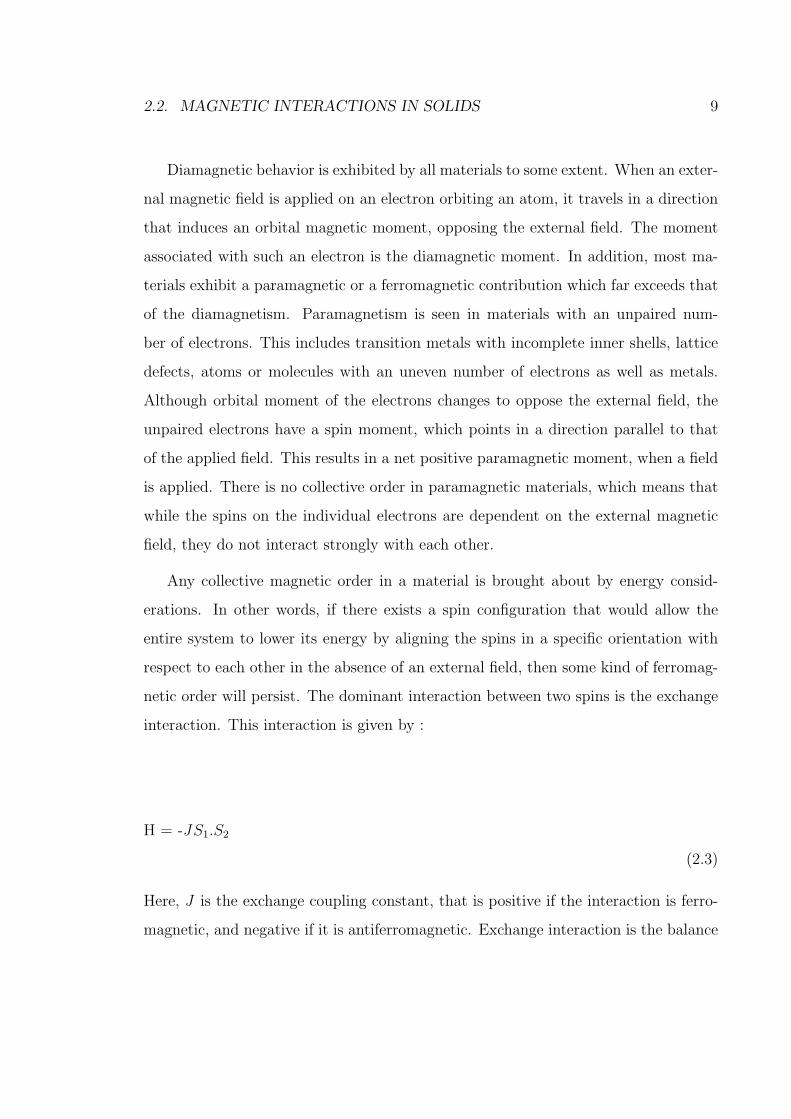
interaction. This interaction is given by :
H = -JS1.S2
(2.3)
Here, J is the exchange coupling constant, that is positive if the interaction is ferro-
magnetic, and negative if it is antiferromagnetic. Exchange interaction is the balance

10 CHAPTER 2. DILUTE MAGNETIC SEMICONDUCTORS
between magnetostatic and electrostatic energies. It can be understood by Pauli’s ex-
clusion principle, which states that no two fermions (electrons, in this case) can have
the exact same quantum state. Consequently, two electrons with the same spin are
spatially separated, thereby decreasing their electrostatic energy. This makes up for
the increase in their magnetostatic energy, which is caused by the magnetic repulsion
of the like spins.
The orientation of a small enough magnetic particles is governed predominantly
by this exchange interaction. However, in a crystal lattice, other longer range interac-
tions such as dipole interactions or anisotropy also begin to affect the magnetization
direction. Dipole energy causes the moments at the surface of a magnetic material
to get oriented along antiferromagnetic directions. On the other hand, anisotropy
tends to orient the magnetic moment along certain crystallographic axes, known as
easy axes. This comes about as a result of spin orbit coupling that results in different
coupling energies along different crystallographic axes. The magnetic behavior of a
material is a result of the sum total of all these interaction energies. In a ferromagnet,
the energy bands are spin-split at the fermi level even when there is no external mag-
netic field present. The exchange interactions in dilute alloys of magnetic elements
are somewhat complex, and are usually understood in terms of hybridization between
the localized spin-split atomic orbitals of the element with the energy bands of the
rest of the lattice. The next section reviews the underlying mechanisms of magnetism
in dilute magnetic semiconductors.
2.3 Models describing magnetism in DMS
The basic model for DMS is of a magnetically inert host semiconductor doped with
localized spins, which may then be doped with electrons or holes. In some cases
such as that of Mn-doped III-V materials, the magnetic ion itself is an acceptor and

2.3. MODELS DESCRIBING MAGNETISM IN DMS 11
acts as a source of holes. The magnetic spins are localized on much smaller scales
than the carriers. The magnetic interactions seen in DMS are governed by an sp-d
exchange, which allows carrier mediated magnetic order and leads to such effects as
a giant Faraday rotation and the formation of bound magnetic polarons. Several
mechanisms have been suggested that explain the origin of magnetism in DMS. Most
theories attempt to identify the various spin coupling energetic concurrent in a system,
and by plugging in the material parameters, attempt to estimate if the energetics lead
to ferromagnetic, antiferromagnetic or spin-glass like interactions between individual
atomic spins.
2.3.1 Mean Field Theory
Zener originally proposed a model for ferromagnetism in dilute alloys of transition
metals, driven by the exchange interaction between carriers and localized spins [11].
The three important ideas behind the model are:
1. In an isolated atom, the lowest energy state is given by the electronic state
where an incomplete d-shell has the highest spin - meaning that all the spins
are aligned.
2. The exchange integral between d-shells of adjacent atoms always leads to anti-
ferromagnetic order
3. The spin of an incomplete shell is strongly coupled to the conduction electrons.
When this coupling dominates over the direct exchange, ferromagnetism is made
possible.
The net spin coupling energy in such a system is a combination of three terms. The
first one is the direct exchange between incomplete d-shell electrons while the second
is the exchange between the d-shell electrons and the conduction electrons. The

12 CHAPTER 2. DILUTE MAGNETIC SEMICONDUCTORS
third interaction is the Fermi kinetic energy of the conduction electrons. This is at a
minimum (0) when there is an even number of spin up and spin down electrons, since
the spin distribution at the Fermi level is balanced. A combination of these three
terms are given by :
Espin = 12αS2
d - βSdSc + 12γS2
c
(2.4)
Here, Sc and Sd are the net spin polarizations of the conduction electrons and the
d-shell electrons respectively. The sign of Espin determines the nature of magnetic
order. While a positive value is indicative of antiferromagnetic order, a negative sign
implies ferromagnetism.
This model was later modified by Dietl et al [9] to understand ferromagnetism in
p-type DMS materials such as GaMnAs. The theory considers ferromagnetic corre-
lation mediated by holes originating from shallow acceptors in the ensemble of the
localized spins in doped magnetic semiconductors. For instance, in GaMnAs, Mn,
which occupies the cation (Ga) sublattice in zinc-blende GaAs provides a localized
spin and at the same time acts as an acceptor. Dietl’s theory can be extended to sev-
eral such p-type DMS, and has been used to estimate Curie temperatures of various
candidates.
2.3.2 Bound Magnetic Polaron
An important attribute of diluted magnetic semiconductors is the sp-d exchange cou-
pling between spins of magnetic ions and those of the impurity electrons in the semi-
conductor band. This results in phenomena such as valence band splitting under
magnetic field and polaron effects. A bound magnetic polaron (BMP) is a collection
of electrons (or holes) bound to impurity atoms through exchange interactions within

2.3. MODELS DESCRIBING MAGNETISM IN DMS 13
an orbit [10]. These interactions can render carriers parallel or anti-parallel to the
magnetic impurity, depending upon the system. These two configurations differ in
energy, and this results in a non-zero spin flip energy that is a characteristic of BMPs.
The net energy of the system can be lowered if the ions are aligned parallel to each
other, since they all interact with carriers the same way. At low temperatures, where
the s-d exchange energy exceeds KBT, mutual alignment of the ions and carriers re-
sults in a ferromagnetic “bubble”. At higher temperatures however, the spins of the
magnetic ions are not constant anymore. A nonzero magnetization results from the
spin fluctuations within any carrier orbit. While the former instance comprises the
“collective” regime, the latter is a characteristic of the “fluctuation” regime.
The temperature up to which a BMP can facilitate magnetic order depends upon
the nature of the interactions between the atomic spins and the charge carriers. The
net exchange has been computed by Durst et al [18] based on the polaron-pair model.
This model considers the interaction between a pair of BMPs via a shared interstitial
area, where the magnetic ions interact with carriers belonging to both the polarons.
Such an area is crucial for carrier mediated ordering of the individual polarons. Fig.
2.2 shows a schematic of the polaron-pair model. The Hamiltonian that results from
this model is given by :
Hm=[(s1.S1)+(s2.S2)]+K’(s1+s2).S3+Js1.s2
(2.5)
where K is the intrapolaron ion-carrier exchange constant,K’ is the interstitial ion-
carrier exchange constant, J is the direct carrier-carrier exchange constant, s1 and s2
are the carrier spins, S1 and S2 are the net polaron spins, and S3 is the collective spin
of the interstitial region.

14 CHAPTER 2. DILUTE MAGNETIC SEMICONDUCTORS
Figure 2.2: Representation of Polaron pair model indicating an interstitial region
Donor bands are relatively large and s-d interactions, weak. Therefore, in cases
where these are involved in the formation of BMPs, the collective phase is observed
only at low temperatures. On the other hand, when the more localized valence bands
are involved, the p-d interaction is strong enough to sustain collective order even at
higher temperatures.
Coey et al [19] have proposed a model for n-type DMS materials based on ex-
change interaction between highly correlated narrow impurity bands and the atomic
spin moment on the dopant ions. Figure 2.3 shows a schematic of the interaction in
oxides, where defects such as oxygen vacancies act as a source of electrons. These
electrons lie in hydrogenic orbitals with characteristic Bohr radii. As their concen-
tration increases, their individual orbits extend out into narrow impurity bands. The
electrons interact with all the magnetic ions that lie within their orbit. Each electron
has an exchange interaction with all the magnetic ions lying within its orbital or
’sphere of influence’. If there are a large enough number of magnetic spins within the
orbital, the electron is completely spin polarized. Furthermore, the atomic magnetic
moments have an indirect exchange interaction mediated by the carriers, that results
in their ferromagnetic ordering.

2.4. SPIN GLASSES 15
Figure 2.3: Representation of Magnetic Polarons in a semiconductor lattice [19]
2.4 Spin glasses
Spin glasses are complex magnetic systems that never equilibrate given any amount
of time. They are comprised of numerous magnetic moments that are constantly in a
state of cooperative relaxation, which can typically only be modeled phenomenologi-
cally.
Glassy behavior was first observed at low temperatures in dilute magnetic alloys
Au:Fe, Ag:Mn and Cu:Mn with Mn concentrations in the range 1-3% was first ob-
served by De Nobel and Du Chantenier (1959) and Zimmermann and Hoare (1960).
They observed an unexplained linear term in the specific heat of these materials which
was independent the Mn concentration. Another curious effect discovered in similar

16 CHAPTER 2. DILUTE MAGNETIC SEMICONDUCTORS
Figure 2.4: Cusp observed in the magnetic susceptibility vs. temperature plot inAu:Fe alloys with 1-2% Fe [20]. Data for 1 % Fe from Lutes and Schmit (1964) arealso included.
dilute alloys by Cannella et al. [20], was a cusp in the magnetic susceptibility (fig.
2.4). This was later understood as the spin glass freezing temperature.
Key ingredients that contribute to glassy behavior in materials are frustration
and quenched disorder. Fig. 2.5 represents these characteristics diagrammatically.
The concept of frustration is understood through the canonical example of antifer-
romagnetically interacting Ising spins on a triangular lattice. For antiferromagnetic
interactions, the lowest energy state for two spins is one in which they point in oppo-
site directions. It is not possible to satisfy all three bonds simultaneously, as having
two spins aligned anti-parallel leads to a conflict for the third spin. More generally,
frustration refers to a situation in which there are competing interactions that cannot
all be satisfied simultaneously.
Frustration alone is not sufficient for spin glass behavior. At low temperatures,

2.5. PROMISING DMS CANDIDATES 17
Figure 2.5: Important characteristics of spin glasses include frustration and quencheddisorder
the magnetic moments in these materials get frozen in an arbitrary state, with no long
range order. Such an ensemble of disordered spins represents a system with quenched
randomness. This can be brought about by disorder of any kind - bond,chemical or
topological. If the single ion anisotropy of the individual spin clusters exceeds long
range order, frustration and quenched disorder can result in spin glass behavior.
2.5 Promising DMS candidates
Regardless of the reason behind the magnetic behavior, the characteristics that are
sought after in novel DMS materials are a high Curie temperature, and a well es-
tablished growth technology. Dietl proposed several suitable candidates as hosts for
DMS based on the mean field theory. All these materials were assumed to be exhibit
p-type conductivity, and the carrier-mediated magnetism was expected to come about
due to sp-d hybridization. However, most of the work published on high temperature
magnetic order DMS materials has involved n-type materials such as Co-doped ZnO

18 CHAPTER 2. DILUTE MAGNETIC SEMICONDUCTORS
Material Eg (eV) Doping µB TC (K) RefGaN 3.5 0.9% Mn 0.9 940 [21]
Cr - > 400 [22]
AlN 4.3 7% Cr 1.2 > 600 [23]5% V 4.2 > 400 [15]
TiO2 3.2 1-2% Co 0.3 > 300 [24]7% Co 1.4 650-700 [25]2% Fe 2.4 > 300 [26]
SnO2 3.5 5% Fe 1.8 610 [27]5% Co 7.5 650 [16]
15% V 0.5 > 350 [28]ZnO 3.3 5% Fe, 1% Cu 0.75 550 [29]
10% Co 2.0 280-330 [30]0.9% Ni 0.06 > 300 [31]
Cu2O 2.0 5% Co, 0.5% Al 0.2 > 300 [32]
In1.8Sn0.2O3 3.8 5% Mn 0.8 > 300 [33]
Table 2.1: High temperature ferromagnetism in n-type DMS [19]
or Mn-doped GaN. Shown in table 2.5 are the reported Curie temperatures of some of
these candidates. Theoretical models based on the formation of impurity bands have
been proposed in order to explain some of these results. Nevertheless, a thorough
understanding of the mechanism behind the magnetic behavior of such n-type DMS
is yet to be firmly established.
The DMS candidate that we have explored in this work, InN is also an n-type
material. The films were deposited over c-sapphire using Molecular beam epitaxy.
GaN buffer layers were employed to accommodate the lattice mismatch between the
film and the substrate. The films were doped with Cr in the range of 0.1-6%, and up
to about 1% Mn. The next few chapters discuss a thorough structural, magnetic and

2.5. PROMISING DMS CANDIDATES 19
electrical investigation of this material. Techniques such as X-ray diffraction (XRD)
and reflection high energy electron diffraction (RHEED) were used for structural char-
acterization and Hall effect measurements for electrical characterization of doped InN
films. Superconducting quantum interference device (SQUID) magnetometry as well
as X-ray magnetic circular dichroism (XMCD) were employed in the investigation of
the magnetic properties. An attempt was made to understand the magnetic behavior
of this novel DMS candidate.

Chapter 3
Growth of InN and doped InN by
MBE
The quest for better DMS candidates has predominantly been dictated by a high Curie
temperature. The more promising candidates turn out to belong to III-V nitride and
II-VI oxide families. A lot of attention has been paid to oxides such as TiO2 and
ZnO as well as nitrides such as GaN and AlN. However, there have been relatively
few reports of diluted magnetic InN alloys [34, 35, 36, 37, 38], despite its attractive
attributes. InN has a low spin orbit coupling of 0.003 eV, as compared to a value of
0.34 eV in GaAs [39]. This translates to a long spin lifetime due to lower spin-orbit
scattering. Furthermore, it also has a high Hall mobility [40] and carrier drift velocity
[41], which could be attractive properties for device applications. The chief issue with
InN is that growth of high quality films is not straightforward. The following section
discusses the chief growth issues and the procedure used for growth of doped InN.
20

3.1. GROWTH OF III-NITRIDES 21
3.1 Growth of III-Nitrides
One of the major challenges in growing epitaxial III-nitrides is the lack of appro-
priately lattice-matched substrate [42]. Like other III-nitrides, InN has a Wurtzite
structure, and ideally requires a substrate with a crystal structure that has three-fold
symmetry. Sapphire is one such substrate with a trigonal lattice structure that is
routinely used for growth of nitrides. However, this is far from ideal, since the lattice
mismatch between sapphire and any of the nitrides is so large that misfit dislocations
are expected at the interface to accommodate the strain [43].
[1120]III−N ‖ [1120]Sapphire [1010]III−N ‖ [1120]Sapphire
AlN -34.6% +13.3%GaN -33.0% +16.0%InN -25.4% +29.2%
Table 3.1: lattice mismatch between sapphire and III-V nitrides
Table 3.1 shows the lattice mismatch values of the nitrides along two different
orientation relationships. The first column shows the mismatch when the [1120]III−N
‖ [1120]Sapphire. In other words, the in-plane axes of the III-N are oriented parallel
to the corresponding axes in the substrate. The second column lists the lattice mis-
match values under the orientation relationship : [1010]III−N ‖ [1120]Sapphire, which
corresponds to the III-N in-plane axes oriented at 30◦ with respect to those of the
substrate. The mismatch values along the second orientation relationship are much
lower in both AlN and GaN compared to that of the first relationship, as depicted for
the case of GaN in fig 3.1. However, InN has comparable mismatch along both these
orientations. Thus, while GaN and AlN have a preferred orientation of deposition
over sapphire, corresponding to that with lower mismatch, InN does not. This results
in yet another challenge in the growth of epitaxial InN films, namely, multi-domain

22 CHAPTER 3. GROWTH OF INN AND DOPED INN BY MBE
Figure 3.1: The preferred orientation of deposition of GaN over sapphire [44]
deposition. InN films grown directly on bare sapphire substrates are not single crys-
tal, but end up with multiple domains including the two mentioned as well as a third
domain corresponding to [1450]InN ‖ [1120]Sapphire [45].
One way to get around this problem is to nitridize the sapphire substrate. This
results in formation of a combination of AlN and AlNOx, depending upon the ni-
tridization temperature [46]. The AlN layer acts as a suitable template for deposition
of InN, and results in the orientation relationship [1010]InN ‖[1010]AlN ‖ [1120]Sapphire.
Alternately, one can deposit thin buffer layers of AlN or GaN over sapphire, prior to
InN deposition, which has the same effect as the nitridized sapphire.
We have used this second approach in this work in order to grow crystalline InN
films. Thin GaN buffer layers grown by CVD were used to accommodate the high
lattice mismatch between InN and Sapphire. In-situ RHEED was used to analyze
the effect of growth temperature and plasma power on the crystalline quality of the

3.2. MOLECULAR BEAM EPITAXY 23
films. X-ray diffraction (XRD) confirmed crystalline films with InN (0001) oriented
parallel to Al2O3 (0001). The following section discusses the growth of InN-based
DMS materials by molecular beam epitaxy.
3.2 Molecular Beam epitaxy
Molecular Beam Epitaxy or MBE was developed in the 1970’s as an alternative to
existing crystalline thin film deposition techniques such as metal-organic chemical
vapor deposition (MOCVD). The key advantage of MBE that distinguished it from
other techniques was the precise control over elemental fluxes in an ultra high vacuum
(UHV) conditions, which allowed deposition of very high quality crystalline films, as
well as atomically abrupt interfaces.
MBE systems are operated in a UHV environment, which corresponds to a pres-
sure range in the order of 1.10−10 Torr. At such low pressures, the level of oxygen or
other contaminants in the chamber is sufficiently low, so that there is minimal incor-
poration of impurities in the films. Furthermore, since the evaporated molecules have
a free path till they hit the substrate, gas phase reactions are also avoided. Deposition
rates in MBE are relatively low, usually lower than 1 A/s. This allows precise control
of layer thicknesses, which is useful for deposition of multi layer device structures.
Figure 3.2 shows a schematic of a typical MBE system similar to the one used used
in this work for growth of InN. Films are deposited by evaporating various sources,
which are pointed in a direction facing the substrate. The sources are usually in
solid form and placed in shuttered ovens known as effusion or Knudsen-cells (K-
cells), where they are resistively heated. When the shutters are opened, the elements
evaporate into gaseous molecules, which move unidirectionally due to the geometry of
the k-cells. Thus formed ’molecular beams’ strike the substrate. Depending on how
much energy a molecule has, it either bounces off the substrate or moves around on

24 CHAPTER 3. GROWTH OF INN AND DOPED INN BY MBE
Figure 3.2: Schematic of Nitride MBE system
the surface until it bonds with another adatom. The UHV environment allows control
over the fluxes of each individual species in order to precisely tailor the composition
of thin film alloys and to vary doping levels in semiconductors.
One important characteristic of MBE is that the substrate temperature used is
much lower than that in other growth techniques such as CVD. This is because the
growth does not depend upon any chemical reactions occurring under equilibrium
conditions. Instead, it relies on providing the individual components at the right flux
ratio, so that they can recombine at the substrate. The bulk diffusion coefficients of
the constituent elements is not large enough at the low growth temperatures. This is
the reason why it is possible to deposit abrupt interfaces by MBE.
The substrate temperature plays a crucial role in the quality of the deposited films.

3.2. MOLECULAR BEAM EPITAXY 25
If it is too high, a large amount of energy is imparted on the incident molecules, mak-
ing them bounce off, thereby leading to a low sticking coefficient. On the other hand,
if the substrate temperature is too low, the adatoms are left with insufficient mobility
to move about on the surface and find an appropriate atom on the previous mono-
layer to attach themselves to. As a result, the films deposited are in the form of rough
3-dimensional islands, and not smooth layers. However, using low growth tempera-
tures results in deposition under non-equilibrium conditions, which can be a powerful
way to grow alloys even with dissimilar constituents. If the energy barrier that must
be overcome in order to transform from a local energy minimum corresponding to a
metastable state into an equilibrium state such as that corresponding to a secondary
precipitate, is larger than the thermal energy of the adatoms, then one can effectively
avoid such phases. Thus there is a tradeoff between structural quality and the ability
to synthesize exotic compounds far from equilibrium conditions.
3.2.1 Growth of InN by MBE
For growth of InN by MBE, while the group III source is solid, a gas source is used
for nitrogen. The gas sources commonly used include NH3 and N2. The dissociation
pressure of InN is relatively low, because of which, its optimum growth temperature
is low compared to that of GaN. This could be a disadvantage while using NH3
as a nitrogen source, since the temperature may not be high enough for effective
decomposition of NH3. This could lead to nitrogen vacancies in the resulting films.
On the other hand, the dissociation energy of N2 molecules is as high as 9.5 eV [42].
Therefore supplying N2 molecules at the substrate surface is not sufficient for any
reaction.
Radio frequency (RF) or electron cyclotron resonance (ECR) plasma sources have
been used to supply the much more reactive atomic nitrogen for the growth of III-
nitrides. One key issue with using plasma sources is that they could produce high

26 CHAPTER 3. GROWTH OF INN AND DOPED INN BY MBE
energy ions that can cause damage during epitaxy [47]. The other problem that they
cause is contamination due to oxygen or carbon dioxide. To prevent this, pyrolytic
boron nitride (PBN) aperture plates are typically used with plasma sources.
The growth temperature is very crucial in determining the quality of films ob-
tained. High growth temperatures above about 550 ◦C result in dissociation of InN.
On the other hand, very low temperatures lead to poor morphology of the films de-
posited. Therefore most groups have reported growth temperatures between 400 and
550 ◦C. Another important parameter that should be controlled in order to obtain
high quality InN is the III/V ratio. A high flux of In leads to the formation of In
droplets, and In-rich films. This is largely because the excess In cannot desorb from
the surface at the typical low growth temperatures. A higher flux of N can be used
to avoid this. However, this again, can increase surface roughening since the migra-
tion of In atoms on the surface is inhibited. Thus the ideal III/V ratio is close to
stoichiometry, on the N-rich side [48].
3.2.2 Reflection High Energy Electron Diffraction (RHEED)
RHEED is an in situ electron diffraction technique which can reveal a lot of informa-
tion about a surface such as roughness, coverage or the coordination and bonding of
the atoms. The RHEED gun emits electron beams with energies in the range of 10 -
20 KeV. The beams are incident at a grazing angle, which is typically well under 5◦.
Due to the grazing angle of incidence, very little momentum gets transferred normal
to the film, and a large area of the surface is probed. This makes RHEED is a surface
sensitive technique.

3.2. MOLECULAR BEAM EPITAXY 27
Figure 3.3: Schematic of RHEED measurement geometry
Figure 3.3 depicts the typical RHEED set up in an MBE chamber. The incident
electron beam gets diffracted off lattice planes parallel the surface, with the diffraction
condition given by :
−−→∆K=
−→G
(3.1)
Where K, the wave vector is given by 2π λ,−−→∆K is the difference between the
incident and diffracted beams and−→G is the reciprocal lattice vector. The relative in-
tensities of the diffracted beams depends upon the morphology of the surface. Planar
2-dimensional surfaces lead to smooth RHEED patterns, whereas surface roughness
or 3-dimensional features such as islands result in spotty streaks. One of the applica-
tions of RHEED is to measure the in-plane lattice parameter in cases where there is
lattice relaxation. Since RHEED is sensitive only to a few monolayers, the interplanar
distance of the top few layers alone can be measured, without averaging out over the
entire film thickness [49, 50]. The spacing between consecutive streaks, t, obtained
along any direction depends inversely upon the interplanar spacing of the planes, and

28 CHAPTER 3. GROWTH OF INN AND DOPED INN BY MBE
is given by :
t = λdparallel
(3.2)
L is the distance of separation between the film and the screen, λ is the wavelength
of the electron beam and dparallel is the interplanar distance between planes parallel
to the electron beam. This can be used to determine the lattice parameters of planes
parallel to the surface.
RHEED measurements were used in this work to monitor the growth process and
to determine optimum deposition conditions. They were also used to examine the
in-plane lattice constant of the Cr-doped films. The following section elaborates the
procedure adopted for growth of InN.
3.3 Growth of Cr and Mn-doped InN
Growth of Cr and Mn-doped InN was carried out in an MBE system that was built by
VG. The pumping on the system included a diffusion pump and a cryopanel, which
was constantly refilled with liquid nitrogen. A phase separator was used to maintain
a closed loop of nitrogen. The pumping geometry allowed a pumping speed of 500
l/s, and the base pressure of the system was typically in the range of 5.10−10 to
1.10−9 mbar. The system had previously been used for deposition of metal films, and
therefore included three electron-beam gun (e-gun) sources in addition to ports for
four effusion-cells. However, for this work, the e-gun sources were not utilized. Instead
effusion cells were used for In, Mn and Cr. A high temperature cell was needed for
Cr, since it has a low vapor pressure at lower temperatures. An RF-plasma nitrogen

3.3. GROWTH OF CR AND MN-DOPED INN 29
atom source was used as the source of atomic nitrogen. The model used was the HD-
25 made by Oxford Applied Research. Purified nitrogen was allowed into the system
through a leak valve, and the pressure of the chamber was maintained at around
2.10−5 mbar during InN deposition. A PBN aperture plate with 10 holes of 0.3 mm
diameter was used at the opening of the source to the chamber. The number of holes
on the aperture plate was relatively small to that used ordinarily in the growth of
III-V nitrides. This small number of holes proved to be a limitation on the amount
of nitrogen available during growth, and hence the growth rate. However, a higher
conductance under the pumping speed would have resulted in the chamber pressure
exceeding the operating limits of the diffusion pump.
The system was equipped with a quartz crystal monitor to measure growth rates
of films deposited. However, this was not adequately sensitive to measure the fluxes
of In, Cr or Mn being used. Therefore, several of the growth runs were monitored by
controlling the temperature of the sources. This gave fairly repeatable growth rates on
a day to day basis. Several calibration runs were made in order to determine growth
rates corresponding to various source temperatures. Typical operating temperatures
were around 750◦C for In, 1100◦C for Cr and 620◦C for Mn. A beam flux monitor was
later built for better control over the flux of incident In atoms prior to deposition.
This monitor was comprised of an ionization gauge mounted at the end of a shaft,
which could be translated in and out of the chamber using a bellowed flange. The
substrates were mounted on a sample stage which rotated in order to maintain the
lateral uniformity of the composition across the wafer. The samples were heated
resistively by a Tantalum heater placed on the back of the stage. The heater could
reach temperatures up to about 550◦C. This was sufficient for most steps involved in
the growth of InN as well as Cr or Mn-doped InN.

30 CHAPTER 3. GROWTH OF INN AND DOPED INN BY MBE
3.3.1 Nitridization of Sapphire
Figure 3.4: Chemistry of nitridization of sapphire [46]
Nitridization of sapphire refers to the surface treatment of the bare substrate at
an elevated temperature under the presence of a reactive nitrogen species, prior to
deposition of III-V nitrides. This step has been shown to result in the formation AlN
or AlNOx) [46, 51]. It has been suggested that active nitrogen reacts with the Al in
sapphire to form AlN, and with the O to form NO. Fig 3.4 shows the possible chemical
reactions that comprise the nitridization process. Depending upon the bonding of
NO, it can either readily desorb or get adsorbed to the Al sites, preventing the
formation of AlN. The latter bonding is favored at higher temperatures, implying
that nitridization at higher temperatures leads to a mixture of AlN and NO, whereas
nitridizing at lower temperatures is more ideally suited to the formation of AlN alone.
The authors of ref. [51] observed this in the RHEED construction obtained at the
end of the nitridization step. A RHEED construction corresponding only to AlN was
observed upon nitridization at 200◦C. Upon increasing the nitridization temperature
to 700◦C, some of the sapphire streaks were still visible in the RHEED construction,
indicating the process remained incomplete.
A similar attempt was made to nitridize a sapphire substrate at a wide range of
temperatures from 100◦C-550◦C. The nitrogen pressure used was 2.10−5 mbar, at a

3.3. GROWTH OF CR AND MN-DOPED INN 31
plasma power of 350 W. Within the temperature range, at every 100◦C, the substrate
was exposed to the nitrogen plasma for about an hour. The RHEED construction
obtained was monitored for any changes. Fig. 3.5(a) shows the RHEED construc-
tion obtained during the process. No change was observed from the sapphire [1120]
RHEED pattern. Nevertheless an InN film was deposited on this substrate.
Figure 3.5: RHEED construction during sapphire nitridization (a) [1120] direction ofSapphire (b) Polycrystalline InN deposited over the substrate
However, this film was observed to be polycrystalline from the RHEED construc-
tion (fig. 3.5 (b)). Thus nitridization of sapphire was unsuccessful within the temper-
ature range accessible by the substrate heater. A potential explanation for this could

32 CHAPTER 3. GROWTH OF INN AND DOPED INN BY MBE
be relatively small nitrogen flux that was available at the sapphire surface. Following
this experiment, further growth of InN was carried out employing a GaN buffer layer.
The details of the growth procedure follow.
3.3.2 Growth of InN and Cr, Mn-doped InN over GaN tem-
plates
The GaN templates employed in the deposition of InN were deposited by MOVPE
at CBL Technologies. The procedure adopted was started with degreasing of the
c-plane sapphire substrates were first degreased and thermally cleaned at 1050◦C for
30 min. The next step was the deposition of low temperature GaN buffer layers at
500◦C, followed by recrystallization at 1050◦C. various thicknesses of GaN were used
in different growth runs. The quality of the InN layers, which were typically under
1000 A in thickness, was not seen to depend upon the thickness of the GaN buffer
layers used.
Following the GaN deposition step, InN buffer and doped layers were grown in
the MBE chamber. Growth proceeded with thermal cleaning of the templates at
500◦C, following which 200-1000 A thick InN buffer layers were deposited at 450◦C.
Thereafter, 200-500 A thick Cr- and Mn-doped InN layers were grown at 350◦C. The
substrate temperature was reduced prior to deposition of the doped layers in order
to prevent formation of secondary precipitates. The nitrogen source was operated
at 350W plasma power with a N2 partial pressure of 2.10−5 mbar. With the In cell
at 750◦C, Cr at 1100◦C and Mn at 620◦C growth rates of the various layers were
low, typically around 90 A/min. Calibration runs were used to keep the growth rates
constant. The Cr doping levels were varied from 0.5% to 6% and Mn from 1% to 2%.
RHEED was used to monitor the depositions. The energy of the electron beam
used was 18.8 keV. Fig. 3.6 shows the RHEED pattern recorded during the deposition

3.3. GROWTH OF CR AND MN-DOPED INN 33
of a 3% Cr-doped film, with the beam parallel to the <1010> direction of InN. Part
(a) shows the RHEED construction that was exhibited by the buffer layer.
Figure 3.6: RHEED construction during deposition (a) InN buffer layer (b) Bufferannealed at 450◦C under N flux (c) Cr-doped InN

34 CHAPTER 3. GROWTH OF INN AND DOPED INN BY MBE
Figure 3.7: SIMS profile of a 5.25% Cr-doped InN film
The spotty-streaks were indicative of roughness in the film. Upon annealing the
film at 450◦C for about 30 min, under a nitrogen flux, the surface roughness, as
observed by RHEED appeared to improve (part (b)). This was followed by deposition
of the Cr-doped InN layer (fig. 3.6(c)).
The films were analyzed by Rutherford backscattering spectroscopy (RBS) and
secondary ion mass spectroscopy (SIMS) for thickness and concentration measure-
ments. The RBS and SIMS data were obtained at IBM Almaden Research Center,
courtesy of Andrew Kellock and Vaughn Deline respectively. Fig. 3.7 shows the SIMS
profile of a 5.525% Cr-doped film. The Cr was seen to form a Gaussian profile near
the surface, in the Cr:InN layer. The total thickness of the film and the concentration
of Cr relative to In were measured by RBS. This information, together with the SIMS
profile was used to determine the thickness of the doped layer, as well as its doping
concentration. Note that the intensities of the various elements were not normalized
by their cross sections, and therefore their relative intensities are not representative
of the sample composition. Instead, RBS was used to confirm stoichiometric In:N

3.3. GROWTH OF CR AND MN-DOPED INN 35
ratio, as well as to determine the Cr doping concentration. Table 3.3.2 shows data
from several films, indicating the fraction of the total sputtering time that was taken
up by the Cr:InN layer.
Sample Time (InCrN : Total) Average % Cr (RBS) %Cr in doped layer(sec:sec)
1641 490:1140 0.4 0.931643 360:1600 0.4 1.771685 167:381 0.8 1.811635 360:640 2.8 5.01681 103:344 1.7 5.53
Table 3.2: SIMS profile of Cr:InN films used to determine composition
Thus Cr and Mn doped InN films were deposited by MBE using GaN templates.
The growth rates were maintained constant by controlling the solid source temper-
atures and the nitrogen pressure. RHEED was used to monitor the growths. The
thicknesses and doping concentrations obtained were measured by using RBS and
SIMS. The next chapters discuss structural, electrical and magnetic characterization
of these films.

Chapter 4
Structural Characterization
One of the main issues with the development of InN based DMS materials is the
ability to grow single crystalline films of reasonable structural quality. The large
lattice mismatch of InN with sapphire, coupled with its tendency to form multiple
crystallographically misoriented domains over this substrate, presents difficulties in
the epitaxy of this material. Growth of high quality films is further deterred by the low
dissociation temperature of InN. This sets a limit on the growth temperature, which,
in turn, leads to roughening and poor quality films. In order to control the magnetic
behavior of InN based DMS, it is important to study the structural properties of this
material.
In this chapter the results of the structural characterization of InN by techniques
such as X-Ray diffraction and transmission electron microscopy are presented. The
effect of doping of the films with Cr and Mn is also studied in detail. A study of the
electrical transport properties made by Hall effect measurements is also presented.
Finally, an investigation of the band gap by photoluminescence measurements are
discussed. The set up and measurement procedures used have been explained before
the data are presented.
36

4.1. TRANSMISSION ELECTRON MICROSCOPY 37
Figure 4.1: TEM of a 100 nm thick InN buffer layer. (a) Shows the bright field image(b) shows the CBED pattern obtained along the InN film
4.1 Transmission Electron Microscopy
Initial structural characterization of a 100 nm thick InN buffer layer deposited over ni-
tridized sapphire was carried out by cross-sectional transmission electron microscopy
(TEM). Figure 4.1(a) shows the TEM bright field image the film. The InN film
appeared to nucleate with a granular structure on the substrate, with the grains
coalescing at higher thicknesses. However, these grains were crystallographically or-
dered, as observed by the consistent convergent beam electron diffraction (CBED)
pattern obtained at various grains (fig. 4.1(b)). Within the grains, several line de-
fects were observed. Thus the InN buffer had several defects, likely due to the large
lattice mismatch between the nitridized sapphire and the film. Further structural
characterization was carried out by X-Ray diffraction.
4.2 X-Ray Diffraction
X-Ray Diffraction (XRD) is a widely used method for characterization of crystalline
materials. It is commonly used as a means for determining crystalline phases present

38 CHAPTER 4. STRUCTURAL CHARACTERIZATION
in a polycrystalline sample, or to determine the crystalline orientation of single-crystal
films. The setup involves an anode, often made of copper, which emits radiation
at a specific wavelength due to electronic transitions. This incident X-Ray is then
monochromated using a crystal monochromator before it is incident on the sample.
Figure 4.2 shows a schematic of the XRD geometry. The incident X-Ray gets
reflected off successive crystalline planes. If the angle of incidence is such that waves
diffracted off successive planes interfere constructively, then an intensity is observed
at that angle by the detector. This relationship is given quantitatively by Bragg’s law
(4.1). An area detector can be used to determine the degree of mosaicity or disorder
in the epitaxial film, since it detects diffracted beams in their off-Bragg condition as
well.
n.λ = 2d.sinθ
(4.1)
Where λ is the wavelength of the incident X-Ray, d is the out-of-plane d-spacing
and θ is the angle of incidence, which is equal to the angle of reflection. If the crystal
is perfect, the peaks obtained at their respective Bragg angles have a full width at
half maximum (FWHM) tending to zero. However, most crystals have structural
imperfections that give them a finite FWHM. Thus the FWHM can be used to gauge
the structural quality of single crystal films.
XRD was used as a tool for structural characterization of epitaxial InN as well
as Cr and Mn-doped InN. The type of measurement made was the 2θ-ω scan. In
order to make this measurement, the angle of the sample stage with respect to the
source, ω (which is numerically equal to θ), is increased in small increments, and the
detector is maintained at an angle of 2θ with respect to the source. Figure 4.3 shows

4.2. X-RAY DIFFRACTION 39
Figure 4.2: X-Ray Diffraction

40 CHAPTER 4. STRUCTURAL CHARACTERIZATION
30 32 34 36 38 40 42
CrN (111)
InN:Cr (0.9%) (0002)
InN:Mn (2%) (0002)
Mn3N
2
(103)
GaN (0002)
2
Sapphire (0006)
Figure 4.3: High Resolution X-Ray Diffraction of Cr- and Mn-doped InN
the typical XRD pattern exhibited by doped InN.
The FWHM of the 2θ-ω rocking curve in most cases was found to be of the order
of 0.1deg, with the (0002) peak of the InN and GaN lined up with the (0006) peak
of sapphire. This is indicative of relatively good crystalline growth. While Cr-doped
InN doped with Cr over a wide range showed no signs of segregation, a clear peak
corresponding to the (103) Mn3N2 peak was observed in several Mn-doped InN films.
In order to gain information about the in-plane orientation of the films, asymmet-
ric peaks were scanned using XRD. These are peaks corresponding to planes whose
axes are not normal to the substrate, but have a component parallel to it. The peaks
that were investigated were those corresponding to the (119) sapphire planes and
(114) InN and GaN planes. The samples were rotated along the Phi direction in or-
der to observe the relative orientations of the InN, GaN and sapphire layers. Figure
4.4 shows the pattern obtained from a typical InN film. The (114) GaN was observed

4.2. X-RAY DIFFRACTION 41
-10 0 10 20 30 40 50 60
Phi
Sapphire (119)
InN (114)
GaN(114)
Figure 4.4: X-Ray Diffraction of Asymmetric peaks of InN

42 CHAPTER 4. STRUCTURAL CHARACTERIZATION
at an angle 30◦ rotated with respect to the (119) Sapphire peak. The InN (114) peak
lined up with the (114) GaN peak. This is an expected result, and is evidence that
the GaN layer did in fact act as a crystallographic template fr InN deposition.
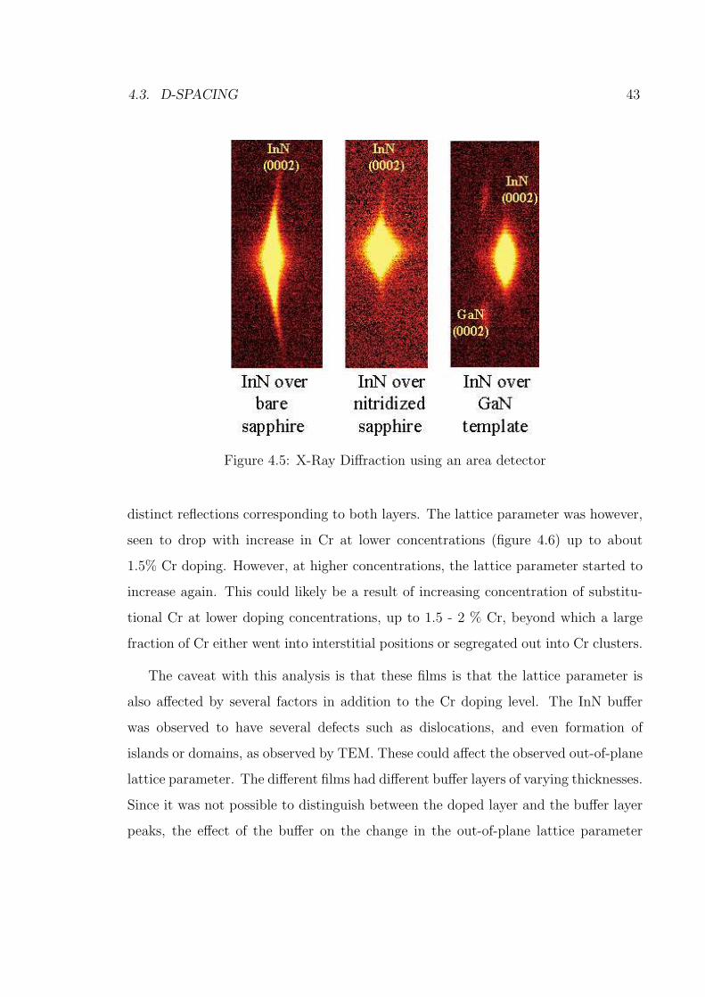
An area detector was also used in order to qualitatively estimate the degree of
disorder in the films. Since an area detector can detect reflections that are off their
Bragg condition, it can be used to observe reflections coming from planes which have
some degree of misorientation or a different lattice constant (figure 4.2(b)). Figure 4.5
shows a comparison between the InN (0002) reflections obtained for films grown under
various growth conditions. Also shown, is the sapphire (0006) peak for reference. The
film deposited on bare sapphire clearly showed the maximum mosaicity, followed by
the film grown over nitridized sapphire. As expected, the film deposited over GaN
showed the smallest width of the InN reflection, indicating the most ordered film.
Another advantage of the area detector is that it can pick up small traces of secondary
elements which do not have any specific crystalline orientation. A peak corresponding
to metal In (101) was seen in some of the In-rich films (not shown), however, no CrN
was observed in any of the films.
4.3 d-spacing
High resolution XRD was used to compute the out-of-plane lattice spacing in several
of the Cr-doped InN films using Bragg’s law. The Cr3+ ion is smaller than In3+,
and the bond length of In-N in the Wurtzite structure is about 2.15 A [52], whereas
that of Cr-N is 2.07 A [53]. Therefore, if all the Cr in Cr:InN went into substitu-
tional positions, the lattice parameter of the alloy would decrease with increase in
doping. Separate diffracted peaks corresponding to the InN and Cr:InN layers were
not observed in any of the Cr-doped films characterized by XRD. Given the struc-
tural disorder in the films, the width of the peaks was not narrow enough in order for
4.3. D-SPACING 43
Figure 4.5: X-Ray Diffraction using an area detector
distinct reflections corresponding to both layers. The lattice parameter was however,
seen to drop with increase in Cr at lower concentrations (figure 4.6) up to about
1.5% Cr doping. However, at higher concentrations, the lattice parameter started to
increase again. This could likely be a result of increasing concentration of substitu-
tional Cr at lower doping concentrations, up to 1.5 - 2 % Cr, beyond which a large
fraction of Cr either went into interstitial positions or segregated out into Cr clusters.
The caveat with this analysis is that these films is that the lattice parameter is
also affected by several factors in addition to the Cr doping level. The InN buffer
was observed to have several defects such as dislocations, and even formation of
islands or domains, as observed by TEM. These could affect the observed out-of-plane
lattice parameter. The different films had different buffer layers of varying thicknesses.
Since it was not possible to distinguish between the doped layer and the buffer layer
peaks, the effect of the buffer on the change in the out-of-plane lattice parameter

44 CHAPTER 4. STRUCTURAL CHARACTERIZATION
Figure 4.6: Out-of-plane d-spacing dependence on concentration
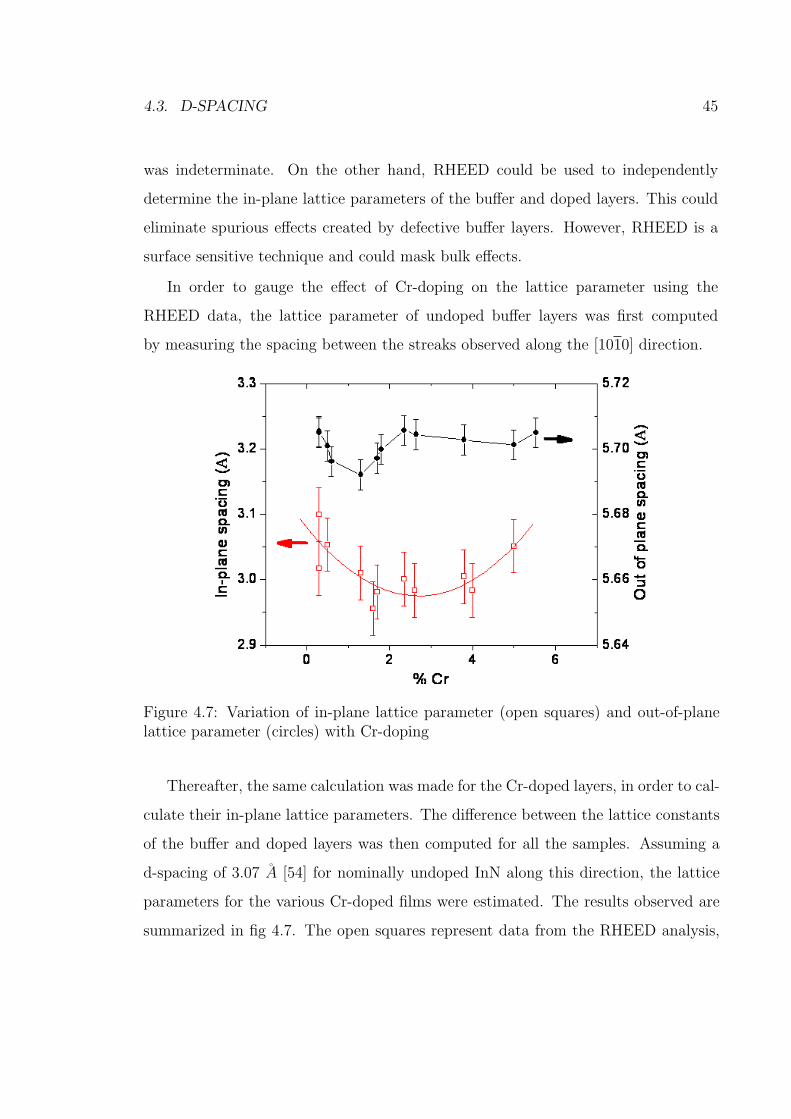
4.3. D-SPACING 45
was indeterminate. On the other hand, RHEED could be used to independently
determine the in-plane lattice parameters of the buffer and doped layers. This could
eliminate spurious effects created by defective buffer layers. However, RHEED is a
surface sensitive technique and could mask bulk effects.
In order to gauge the effect of Cr-doping on the lattice parameter using the
RHEED data, the lattice parameter of undoped buffer layers was first computed
by measuring the spacing between the streaks observed along the [1010] direction.
Figure 4.7: Variation of in-plane lattice parameter (open squares) and out-of-planelattice parameter (circles) with Cr-doping
Thereafter, the same calculation was made for the Cr-doped layers, in order to cal-
culate their in-plane lattice parameters. The difference between the lattice constants
of the buffer and doped layers was then computed for all the samples. Assuming a
d-spacing of 3.07 A [54] for nominally undoped InN along this direction, the lattice
parameters for the various Cr-doped films were estimated. The results observed are
summarized in fig 4.7. The open squares represent data from the RHEED analysis,

46 CHAPTER 4. STRUCTURAL CHARACTERIZATION
Figure 4.8: Schematic of Photoluminescence in a direct band gap material
whereas the circles show the out-of-plane lattice parameter measured by XRD, for ref-
erence. Schematically, the in-plane lattice parameter showed similar behavior to that
of the out of plane lattice constant, dropping in value at lower values of Cr-doping
and increasing beyond a doping level of about 2%.
Once again, this was only a qualitative observation, and the actual amount of Cr
incorporated in the lattice could not be quantitatively calculated. This is because
the lattice parameter also varies depending upon other factors such as antisite de-
fects. Nevertheless, the structural data was taken as evidence that Cr doping led to
substitutional Cr only at lower doping levels, following which, it probably dissolved
as interstitial Cr or segregated into metal rich clusters. This had an effect on the
magnetic behavior of these films as well. This is discussed in greater detail in the
next chapter.

4.4. PHOTOLUMINESCENCE 47
4.4 Photoluminescence
Certain materials can release the energy they absorb from an external source in the
form of radiation. This process is known as luminescence. In order to produce lu-
minescence, electron-hole pairs must first be created, which subsequently recombine
to produce the radiation. For this purpose, excitation energy can be provided in
several ways such as by using a light source or by applying an electric field. Photo-
luminescence (PL) occurs as a result of photon absorption, when a radiative source
such as a laser is used for excitation (fig 4.8). The incident photons must have an
energy that exceeds the band gap value of the material, sufficient to excite electrons
from the valence band to the conduction band, leaving behind excited holes. These
electrons and holes quickly relax by losing their energy non-radiatively to phonons.
While electrons settle at the bottom of the conduction band, holes move to the top
of the valence band. The electrons and holes can relax further by recombining either
radiatively or non-radiatively. The total relaxation time, t, is given by the following
expression:
1t
= 1tr
+ 1tnr
(4.2)
Here, tr and tnr are the radiative and non-radiative lifetimes respectively. In direct
band gap semiconductors such as the III-Vs, the top of the valence band is lined
up with the bottom of the conduction band in momentum or k-space. This allows
direct recombination without an intermediate phonon interaction, unlike in the case
of indirect band gap semiconductors, where momentum conservation requires that
the recombination is phonon assisted. Therefore, the efficiency of radiative recom-
bination is much higher for these materials than in indirect semiconductors such as
48 CHAPTER 4. STRUCTURAL CHARACTERIZATION
Si. This property is utilized in order to measure the band gap of direct band gap
semiconductors. A pump laser emits photons with an energy exceeding the band gap,
which results in the semiconductor luminescing at its band gap energy.
The most commonly quoted band gap value for InN, which is also a direct band
gap semiconductor, is 1.89 eV at room temperature [55]. Most of the earlier band
gap studies on InN films were done by measuring optical absorption, and not pho-
toluminescence since the material quality was not good enough for photon emission.
Photoluminescence (PL) in InN films was first reported in 2001. With the realization
of high quality InN film several groups studied the PL measurement in the single
crystalline InN films. These films were grown by modern deposition techniques such
as MOVPE or MBE. The band gap energy of InN was discovered to be much smaller
than earlier reported 1.89 eV [56, 57, 58]. In fact, it was found to lie around 0.90
eV. This created a controversy about the exact band gap energy, especially because
the newly reported small band gap values were compatible with the wavelength of
the optical fiber. Therefore, if high quality InN films with a direct band gap of 0.65
0.90 eV can be grown, could have potential applications in high speed LEDs and
photodiodes (PDs). With progress in the growth procedure of InN, it has been fairly
well established that the band gap is around 0.65 - 0.9 eV.
PL measurements were used to measure the band gap of the InN as well as Cr:InN
in this work. An Ar ion laser with a wavelength of 514.5 nm was used as a pump source
with a constant incident pump power of 250 mW. An InGaAs photodiode measured
the optical spectrum. Fig 4.9 shows the PL data taken at room temperature. The
intensities are presented on a log scale. Luminescence was observed at 0.84 eV,
which is quite consistent with values reported in the literature. The peak was not
significantly shifted in the Cr-doped films. However, the intensities on the PL peaks
was much lower in Cr-doped films than in nominally undoped InN. This was likely
due to poorer quality of Cr-doped films owing to their lower deposition temperatures.

4.4. PHOTOLUMINESCENCE 49
Figure 4.9: Photoluminescence observed in Cr-doped InN

50 CHAPTER 4. STRUCTURAL CHARACTERIZATION
4.5 Hall Effect Measurement
The electrical behavior of the InN and Cr:InN films was studied using Hall effect
measurements. The Hall effect arises from the interaction of charge carriers in a
semiconductor with an applied electric field in the presence of a magnetic field. Figure
4.10 shows a schematic representation of the setup, where a potential (Vapp) and a
magnetic field (B) are applied across a semiconducting samples along orthogonal
directions. An electron moving with a velocity −→v , in the potential applied feels a
Lorentz force given by :
F = e−→v xB
(4.3)
Holes in the semiconductor experience a similar force along the opposite direction,
leading to an accumulation of charge carriers along opposite edges of the semicon-
ductor. This, in turn, gives rise to electrostatic forces, which, at equilibrium, are
equal and opposite the Lorentz force. Thus a potential develops along this direction,
perpendicular to the applied voltage. This potential is known as the Hall voltage,
and is give by :
VH = IB/ned
(4.4)
Where, n is the density of charge carriers, e is the electron charge and d is the thickness
of the film. The sign of VH gives information whether the material is n-type or p-
type. The sheet resistance of the film can also be measured using the standard Van
Der Pauw technique. This can be used together with VH to calculate the mobility,

4.5. HALL EFFECT MEASUREMENT 51
Figure 4.10: Hall Setup
µ. This is given by :
µ = V H/RSIB = 1/enSrS
(4.5)
4.5.1 Hall Effect measurements on InN and Cr:InN
The high n-type carrier concentration in III-Nitrides has been attributed to both
nitrogen vacancies as well as oxygen [59] incorporation in the films. There are several
sources of oxygen in the growth process. For instance, in MOCVD, the ammonia
precursor could contain oxygen, and in MBE the background water pressure in the
chamber, oxygen from the sapphire substrate or from the quartz cavity on some
plasma sources could all lead to oxygen incorporation.

52 CHAPTER 4. STRUCTURAL CHARACTERIZATION
Hall effect measurements were used in order to get an idea of the type of con-
duction, as well as the mobility. Indium contacts were used in the four point probe
configuration. The Hall setup described above was used, with sheet resistance calcu-
lated by the Van Der Pauw method. The Hall set up was used to determine the sheet
carrier concentration and mobility. As expected the films were observed to exhibit
n-type conduction.
Table 4.5.1 sums up the data obtained for some InN and Cr:InN films. The
sheet concentration obtained varied from about 3.1014 to 1.1015 cm−2. Based on the
assumption that all the conduction occurred through the InN (and InN:Cr) layers,
and not the buffer GaN layers, this yielded a carrier concentration between 1.1019 and
1.1020 cm−3. Cr-doping did not seem to have an effect on the carrier concentration.
This is reasonable since Cr has the same valence as In, and neither acts as a donor, nor
an acceptor in InN. Polycrystalline (sample 1591) as well as crystalline InN (sample
1625) films grown directly over sapphire also exhibited n-type behavior. The mobility
of the films was relatively low, in the range of 25 - 100 cm2V−1s−1. High mobility of
over 3000 cm2V−1s−1 has been observed in high quality InN films [60]. The films in
question were much thicker than our InN films, at about 7500 nm. Thus they were
presumably relatively more defect-free than the ones discussed in this work, which
explains the better electrical properties.
Sample No. Description n (cm−3) Mobility(cm2V−1s−1)
1591 90nm Polycrystalline InN 5.69E+19 25.31593 105nm InN/GaN 1.46E+20 40.21625 45nm InCrN/100nm InN/Sapphire 6.46E+19 25.81639 35nm InCrN/90nm InN/GaN 8.74E+19 97.31642 30nm InCrN/140nm InN/GaN 1.84E+19 76.6
Table 4.1: Hall effect measurement on InN and Cr:InN films
The structural properties of InN as well as Mn and Cr:InN were thus examined

4.5. HALL EFFECT MEASUREMENT 53
by a variety of characterization tools. The films were seen to have relatively good
crystalline quality, with the [0001] direction of InN and GaN pointing parallel to
the c-axis of the substrate. The FWHM of the 2θ-ω XRD curve was 0.1◦. While
secondary phase formation was observed in Mn:InN, Cr:InN did not appear to have
any other phases. However, an examination of the lattice constant of Cr-doped films
revealed that large fractions of the dopant likely went into interstitial positions, or
somehow precipitated out above a doping level of about 1 - 2%. PL measurements
revealed a band gap around 0.84 eV in InN and Cr:InN, which is consistent with
values reported in the literature. Hall effect measurements revealed n-type behavior
in these materials with very high carrier concentrations between 1.1019 and 1.1020
cm−3 . The mobilities were not very high, since the film thicknesses were relatively
low compared to that of high quality InN films. The magnetic properties, and the
effect of the structure of the Cr:InN films on them is discussed in the next couple of
chapters.

Chapter 5
Magnetic and Electrical
Characterization
5.1 Magnetic Characterization
The magnetic behavior of doped InN was measured by Superconducting Quantum
Interference Device (SQUID) magnetometry. The magnetometer used in this work
was designed by Quantum Design, and uses a radio-frequency (RF) SQUID. An
RF SQUID is based on a superconducting coil with a thin insulator sandwiched
in-between, which leads to the formation of a Josephson junction (fig 5.1). The elec-
tron pairs that are responsible for zero resistance conduction in a superconductor are
phase-coherent over long distances. Thus the electrons carrying current in the super-
conducting coil travel as waves, with a constant phase at any point on the coil. A
small change in magnetic flux through the superconducting coil changes the momen-
tum of the electrons, thereby changing their phase. Quantum mechanical boundary
conditions due to which the phase change through the entire coil must be an integral
multiple of 2Π , determine the allowed quantized values of change in magnetic flux
through the coil. Any excess change in flux is balanced out by a small current that is
54
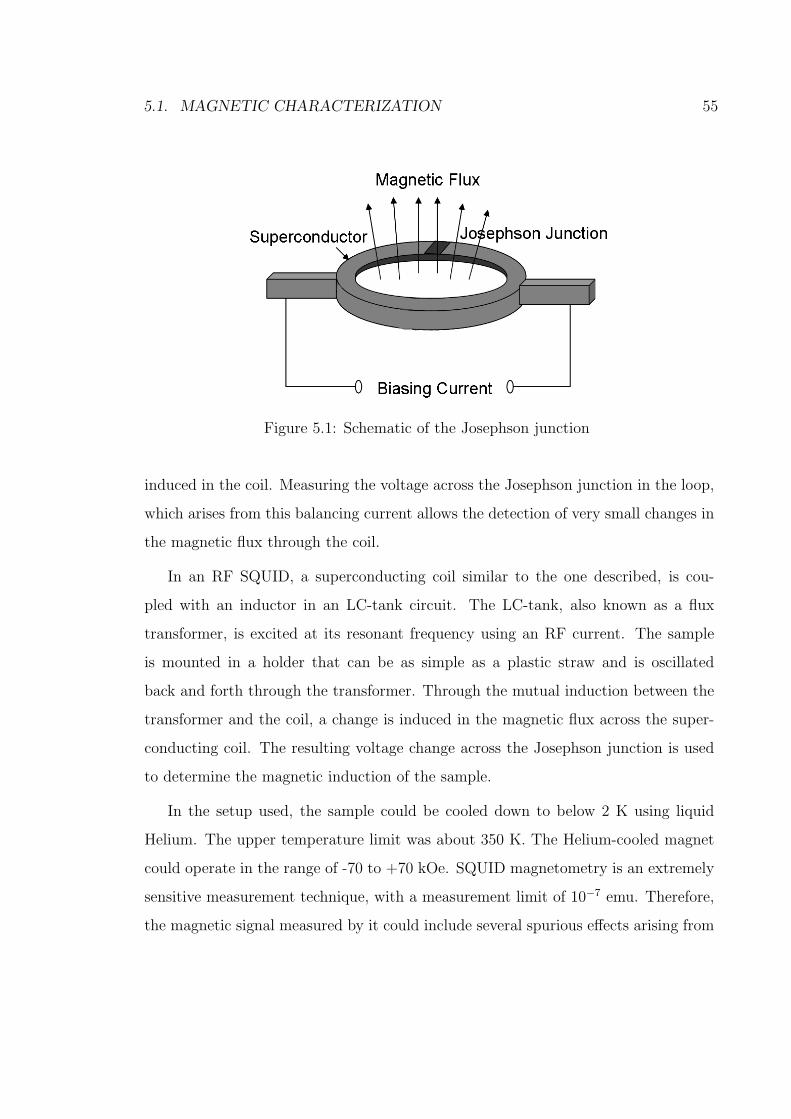
5.1. MAGNETIC CHARACTERIZATION 55
Figure 5.1: Schematic of the Josephson junction
induced in the coil. Measuring the voltage across the Josephson junction in the loop,
which arises from this balancing current allows the detection of very small changes in
the magnetic flux through the coil.
In an RF SQUID, a superconducting coil similar to the one described, is cou-
pled with an inductor in an LC-tank circuit. The LC-tank, also known as a flux
transformer, is excited at its resonant frequency using an RF current. The sample
is mounted in a holder that can be as simple as a plastic straw and is oscillated
back and forth through the transformer. Through the mutual induction between the
transformer and the coil, a change is induced in the magnetic flux across the super-
conducting coil. The resulting voltage change across the Josephson junction is used
to determine the magnetic induction of the sample.
In the setup used, the sample could be cooled down to below 2 K using liquid
Helium. The upper temperature limit was about 350 K. The Helium-cooled magnet
could operate in the range of -70 to +70 kOe. SQUID magnetometry is an extremely
sensitive measurement technique, with a measurement limit of 10−7 emu. Therefore,
the magnetic signal measured by it could include several spurious effects arising from

56 CHAPTER 5. MAGNETIC AND ELECTRICAL CHARACTERIZATION
Figure 5.2: Typical magnetic hysteresis of ferromagnetic materials
magnetic inclusions or precipitates in the films, or contamination introduced during
sample handling. Nevertheless, this was the primary magnetic characterization tool
that was employed to study the temperature and field dependent behavior of the Cr
and Mn-doped samples.
All ferromagnetic materials exhibit magnetic hysteresis, when subjected to an ex-
ternal magnetic field. Fig 5.2 shows the typical hysteresis obtained by a ferromagnet.
As the external field is increased, the magnetization of the sample also increases till
its magnetization reaches a saturation value, given by Ms. Thereafter, even if the
field is completely removed, the sample still retains some of its magnetization, known
as remanence or MR. If the external field is now reversed, the magnetization slowly
drops, until it is completely demagnetized, at a value for the external field correspond-
ing to the coercive field, or HC . Thus the sample absorbs energy from the externally
applied magnetic field.

5.2. MAGNETIC BEHAVIOR OF CR AND MN-DOPED INN 57
The shape of the hysteresis curve is also indicative of whether the sample is mag-
netized along its easy or hard axis. The difference between these two axes is that the
magnetization of a sample can be saturated along its easy axis with a much lower
external applied field, than what is required to saturate the sample along its hard
axis. The anisotropy of a sample is the energy required to flip its magnetization from
the easy to the hard axis. The reason for anisotropy is the coupling between the spin
magnetic moment and the crystal lattice. Anisotropy can come about from various
sources such as shape of the sample, or crystalline orientation, stress etc.
5.2 Magnetic behavior of Cr and Mn-doped InN
Most Cr-doped films exhibited magnetic hysteresis from 5 K up to room temperature.
Fig 5.3(a) shows the magnetic hysteresis of a 0.9% Cr-doped InN sample, with the low
field behavior shown in 5.3(b). A small coercivity of about 100 Oe was observed in this
as well as several other samples. The hysteresis was rounded in shape, which could
indicate partial demagnetization at low fields. This behavior has been observed in
several nitride DMS materials [61, 62]. The hysteresis was corrected for a diamagnetic
background, measured at 300 K from 30 to 70 kOe. This background was attributed
to the sapphire substrate and buffer layers. The background was measured from
the hysteresis at 300 K since the paramagnetic background is negligible at higher
temperatures. The additional paramagnetic background seen at 5 K under high
fields was attributed to imperfections in the InN buffer layers resulting from the large
lattice mismatch of 10% between GaN and InN and was also observed in undoped
InN films (not shown). Mn-doped samples, however, showed very weak hysteresis at
low temperatures and none at room temperature. This is consistent with XRD that
suggested a lack of solubility of Mn in InN.

58 CHAPTER 5. MAGNETIC AND ELECTRICAL CHARACTERIZATION
Figure 5.3: Magnetic behavior of 0.9% Cr-doped InN. (a)Shows magnetic hysteresisobserved at various temperatures. (b) Shows the low field behavior

5.2. MAGNETIC BEHAVIOR OF CR AND MN-DOPED INN 59
Temperature dependence of remanent magnetization was measured from 5 to 350
K. The moment of the samples was saturated by applying a field of 50 kOe prior to
each measurement. While Cr-doped films exhibited a steady drop in remanence with
increase in temperature, indicating magnetic order (Fig 5.4(a)), Mn-doped samples
showed paramagnetic behavior (Fig 5.4(b)), with a 1T-like temperature dependence.
Cr-doped samples exhibited a signal arising from two distinct contributions. The high
remanence seen at low temperatures was attributed to the paramagnetic background
from the InN and GaN buffer layers and was observed in undoped films as well
(not shown). At higher temperatures, Cr-doped films exhibited a smooth drop in
remanence with temperature, indicating magnetic order. The shape of the remanence
was different from that observed in conventional ferromagnets, however was quite
similar to that observed in several n-type DMS such as Mn:GaN. In contrast, Mn-
doped and undoped films showed no temperature dependence of remanence in this
region. The difference in magnetic behavior between Cr- and Mn-doped InN can, once
again, be ascribed to secondary phases. Mn forms several compounds with N, most of
which, including Mn3N2, are antiferromagnetic with high Neel temperatures [14, 63]
The small magnetic moment observed in InN:Mn is likely due to uncompensated spins
resulting from clusters of Mn3N2 randomly distributed in the InN matrix, whose
presence was confirmed by X-Ray diffraction. On the other hand, Cr essentially
forms only one compound, CrN, with N. Although it can purportedly react with
N to form Cr2N, there are no experimental accounts of this compound. CrN is an
antiferromagnet with a Neel temperature of 273 K [64]. Although this compound
was not observed by high resolution X-Ray diffraction, this was insufficient proof of
its absence in Cr:InN. Instead, other indirect tools such as the magnetic signature
of this phase, and spectroscopy at the Cr L-edge were used to probe deeper into
the possibility of potential precipitation of CrN. For this purpose, CrN films were
deposited on two different substrates.

60 CHAPTER 5. MAGNETIC AND ELECTRICAL CHARACTERIZATION
Figure 5.4: Magnetic remanence of doped InN. (a) Cr:InN shows steady decrease inMR with temperature. (b) Mn:InN shows paramagnetic remanence behavior

5.3. NORMALIZED SATURATION MAGNETIZATION MOMENT 61
Figure 5.5: Small anisotropy observed in 1.8% Cr-doped InN. In-plane easy axis (opensquares) and out of plane hard axis (circles)
A small anisotropy was also observed in Cr:InN, as depicted in fig 5.5. The easy
axis was observed to be in the plane of the film, while the out of plane axis was the
hard axis.
5.3 Normalized saturation magnetization moment
The saturated magnetic moment of Cr-doped InN at 300 K was normalized per unit
Cr atom for a wide range of Cr-doped films. In order to make this calculation, the
saturation moment observed at 300 K was divided by the volume of the Cr-doped
film and the doping level. Fig 5.6 shows the summary of the observed normalized
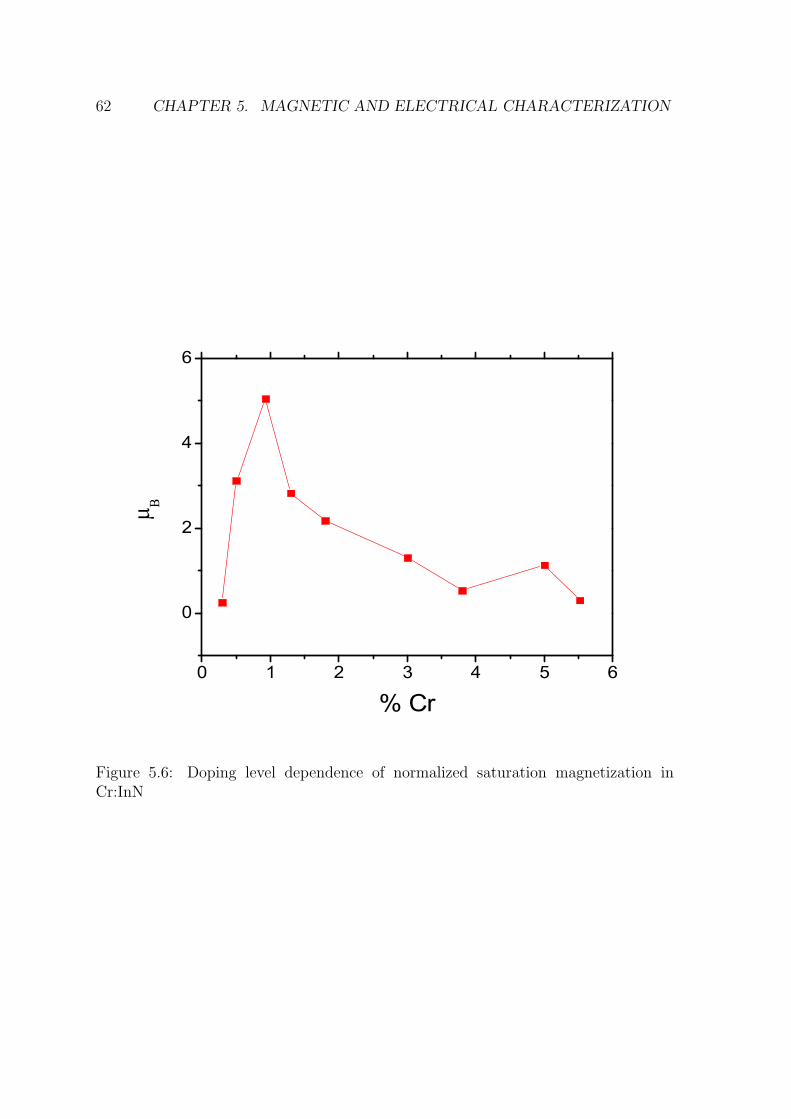
62 CHAPTER 5. MAGNETIC AND ELECTRICAL CHARACTERIZATION
0 1 2 3 4 5 6
0
2
4
6
% Cr
Figure 5.6: Doping level dependence of normalized saturation magnetization inCr:InN

5.3. NORMALIZED SATURATION MAGNETIZATION MOMENT 63
moment. The moment had a peculiar dependence upon doping concentration. At
lower concentration levels, below about 1% Cr, it tended to rise with increase in dop-
ing, dropping off thereafter. Some of the behavior could be explained by correlating
the magnetism with the structural behavior. Both XRD and RHEED indicated sug-
gested that an Cr increasingly dissolved in the InN matrix up to about 1-2% doping,
as suggested by the in-plane as well as out-of-plane d-spacing reducing in this range.
This would suggest that more and more Cr went into substitutional positions as the
nominal Cr doping was increased, thereby causing a rise in the moment per Cr. The
mechanism by which this would happen is not obvious. One could potentially model
this system in a manner similar to that of Gd:GaN [14], where the magnetic ions have
a region of influence in their vicinity that they magnetically polarize. Such a theory
could explain the relatively large moment obtained per Cr atom, which was as high
as 5 µB in the case of the 0.9% Cr-doped film.
At higher Cr doping levels, the normalized magnetic moment was observed to
fall off as the doping level increased. This observation was consistent with the the
structural analysis, which suggested that large fractions of Cr were likely present in the
form of precipitates or went into interstitial positions, rendering them magnetically
inactive. This was also corroborated by the higher paramagnetic moment exhibited
at lower temperatures by films with higher Cr doping than that shown by comparable
films with a lower Cr doping level. Fig 5.8 shows this behavior in two films - one
with 5.5% Cr and the other with 0.9% Cr. The magnetic moment measured has
been normalized per Cr atom in both cases. As observed, the film with higher Cr
concentration exhibits a larger slope at higher fields, indicating greater paramagnetic
contribution. Furthermore, signs of low temperature paramagnetic ’blocking’ were
observed in some of the films with a higher Cr concentration, pointing towards the
formation of paramagnetic clusters. This is discussed in more detail in the following
sections.

64 CHAPTER 5. MAGNETIC AND ELECTRICAL CHARACTERIZATION
Figure 5.7: Doping level dependence of normalized saturation magnetization inCr:InN

5.3. NORMALIZED SATURATION MAGNETIZATION MOMENT 65
Figure 5.8: A comparison of the magnetic hysteresis obtained at 20 K from a 0.9%Cr:InN(open circles) film with that of a 5.5% Cr:InN (squares) film

66 CHAPTER 5. MAGNETIC AND ELECTRICAL CHARACTERIZATION
Figure 5.9: Field cooled vs. Zero field cooled measurements.
5.4 Spin-Glass like Behavior
5.4.1 Measurement Procedure
Field-cooled vs zero-field cooled (FC/ZFC) measurements are used to study the in-
fluence of the sample history on its temperature dependent magnetization. The tech-
nique attempts to determine if it is possible to freeze any spin clusters by applying
a magnetic field at lower temperatures. Figure 5.9 shows a schematic of the how the
measurement is made. During the field cooled measurement, a high field, typically 50
kOe is applied in order to saturate the film following which, it is cooled down. The
sample is subsequently warmed up under a much smaller field, of the order of 100 Oe.
If the film is comprised of clusters, their moments get saturated. When the sample
is heated up under a much smaller field, domain formation reduces the moment. The
zero field cooled measurement involves cooling the sample under 0 magnetic field.

5.5. METASTABLE BEHAVIOR 67
The clusters, which have random spin orientations, get frozen in their orientation.
Now during the warm up step, the domains orient themselves with the external field.
This causes an increase in the magnetization as temperature is increased up to a
point, beyond which it drops again. While a separation of the FC and ZFC curves
is indicative of hysteretic behavior, a cusp in the ZFC trace is a clear indicator of
spin-glass or cluster-glass behavior.
5.4.2 FC/ZFC measurements in Cr-doped InN
The magnetic behavior of Cr-doped InN was probed deeper by means of FC vs.
ZFC measurements. Fig 5.10 shows the FC vs.ZFC traces observed in a 2.5% Cr-
doped InN film. A clear separation was observed between the two traces for the entire
temperature range, indicating hysteretic behavior above room temperature. However,
this measurement did not indicate conventional ferromagnetism, since the tendency
to form a broad cusp-like feature was observed at relatively high temperatures. All
Cr-doped films in the Cr-doping range from 0.5-6% Cr exhibited this behavior, where
a cusp could not be observed since the samples could only be measured up to about
350 K. Thus the Cr:InN exhibited spin-glass like behavior.
5.5 Metastable behavior
In addition to the FC/ZFC behavior which indicated a deviation from traditional
ferromagnetism, Cr:InN also exhibited metastability in its temperature dependence
of remanent magnetization. Figure 5.11 shows the typical measurements made that
revealed this behavior. A 0.9% Cr:InN film was first cooled down to 5 K and a field
of 50 kOe was applied to saturate the sample. The field was then set to zero again
followed by the measurement of the remanence while warming up the sample to 300
K. The remanence was seen to smoothly decrease with temperature. Subsequently,

68 CHAPTER 5. MAGNETIC AND ELECTRICAL CHARACTERIZATION
0 100 200 300 400
3.6x10⁻⁶
4.5x10⁻⁶
5.4x10⁻⁶
6.3x10⁻⁶
M (e
mu)
Temperature (K)
ZFC (warmed under 100 Oe)
FC (warmed under 100Oe)
Figure 5.10: Field cooled vs. Zero field cooled measurements in a 0.9% Cr-dopedInN.

5.5. METASTABLE BEHAVIOR 69
Figure 5.11: Remanence dependence on temperature in 0.9% Cr-doped InN. Increasein remanence due to application of magnetic field observed.
the sample was again saturated at 300 K in a field of 50 kOe, the field is switched
off, and the remanence was now measured while cooling the sample down to 5 K.
Two surprising observations were noted which are atypical for common ferromagnets.
First of all, after applying the external field, the remanence increased by about 10%
as compared to its value at the end of the warm-up. We referred to this effect as
∆MR. Secondly, the remanence did not increase with decreasing temperature but
stayed constant.
Fig. 5.12 shows the dependence of ∆MR on the warm up temperature. This data
was obtained by warming up to different end temperatures, followed by applying a
field of 50 kOe before the subsequent cool down. The increase in remanence was
observed only down to 200 K, below which, no such effect was observed. Below

70 CHAPTER 5. MAGNETIC AND ELECTRICAL CHARACTERIZATION
200 K, the remanence previously measured while warming could be re-established by
applying 50 kOe, while at higher temperatures from about 250 K up to 400 K a ∆MR
as high as 13% was obtained, with a 2-3% uncertainty.
An explanation of these findings is not obvious. The reduction in remanence with
warming could potentially arise from magnetic domain formation, which are removed
upon application of external field, thereby leading to an increase in remanence. How-
ever, this is not a plausible explanation as it assumes that either this domain formation
occurs only above 200 K. This would imply that below this temperature, relaxation
originates from other mechanisms such as spin waves or magnetic fluctuations, which
are typically reversible with temperature. However, this is in contradiction with the
remanence staying constant with cool down. The other possibility is that magnetic
domains do exist below 200 K, but 50 kOe is insufficient to remove them. However
this is not likely, since 50 kOe is sufficient to reestablish the remanence at lower
temperatures. Thus the ∆MR and its temperature dependence do not seem to have
an explanation which point in the direction of traditional ferromagnetism, and sug-
gest spin glass like behavior. Comparable observations were also made in a Gd:GaN
sample with a Gd concentration of about 2.1019cm−3 [65].
Since the remanence exhibited metastable behavior, its relaxation behavior with
time was also looked into. The 0.9% Cr:InN films was subjected to a magnetic
field of 50 kOe to saturate it. The field was then removed, and the remanence was
measured as a function of time. Fig. 5.13 shows the summary of the results obtained.
The measurement was made at 300 K and 350 K. As observed, the remanence stayed
constant over a timescale of hours, showing no tendency to relax. Thus the metastable
behavior was temperature dependent, but not time dependent. This could indicate
that the spin glass freezing or ordering temperature for this material is well above
350 K.
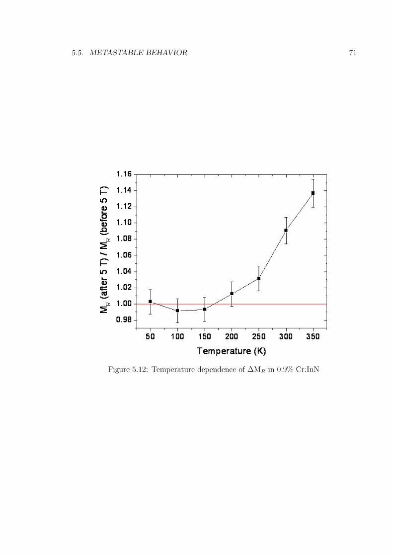
5.5. METASTABLE BEHAVIOR 71
Figure 5.12: Temperature dependence of ∆MR in 0.9% Cr:InN

72 CHAPTER 5. MAGNETIC AND ELECTRICAL CHARACTERIZATION
Figure 5.13: Remanence stays constant with time in 0.9% Cr-doped InN.
5.6. EVIDENCE OF SPIN POLARIZED CARRIERS 73
5.6 Evidence of spin polarized carriers
Hall effect measurements suggested n-type conductivity in Cr:InN, as discussed in
chapter 4. Ferromagnetic materials exhibit a Hall resistance, which carries an addi-
tional term, proportional to their magnetization. This phenomenon is known as the
anomalous Hall effect. It occurs as a result of spin orbit coupling between spin polar-
ized carriers in a spin-split band, that leads to asymmetry in orbital momentum. The
anomalous Hall coefficient is much larger than the normal coefficient, and it tends to
saturate at high fields. Thus the net Hall resistivity of a ferromagnet can be given by
the relation :
ρH = R0µ0H + RsM
(5.1)
Here, ρH is the net resistance, µ0H is the magnetic induction, Rs is the anomalous
Hall coefficient, and M is the magnetization of the material. A description of this
effect in III-V DMS is based on the mean field theory, whereby, the valence band is
spin-split due to exchange interaction with transition metal moment. This interaction
leads to an additional term in the Hamiltonian [66], given by :
Hsplit = hm.−→s(5.2)
Where, m corresponds to the localized moment of Mn atoms, −→s is the spin of an
electron and h is proportional to the average magnetization field, and is non-zero only

74 CHAPTER 5. MAGNETIC AND ELECTRICAL CHARACTERIZATION
in the ferromagnetic state. If the Mn is fully polarized, then
H = NMnJpdS
(5.3)
where S is the spin of the polarized Mn (5/2), NMn is the density of Mn atoms
and Jpd is the exchange interaction between the local moments and the valence band
electrons. This leads to an effective magnetic field within the crystal, which, alongside
spin orbit coupling is responsible for giving rise to the anomalous hall effect (AHE).
Figure 5.14: Schematic of the Physical Property Measurement System (PPMS) :Courtesy Quantum Design
The geometry used for measurement of anomalous Hall effect (AHE) in Cr:InN was
the same as that for the Hall effect. A four point probe method was used, via Indium
contacts on the films. The magnetic field applied out of plane was varied in magnitude,
in order to measure any hysteretic behavior of the carriers. The measurements were

5.6. EVIDENCE OF SPIN POLARIZED CARRIERS 75
made on a physical property measurement system (PPMS) built by Quantum Design
(fig. 5.14). The system is designed to make measurements over a temperature range
of 2 K - 400 K. The applied magnetic field could be varied from -70 kOe to 70 kOe.
The Hall voltage of several Cr-doped InN films was measured using this setup
using an AC excitation voltage, whose magnitude was varied. While most films only
showed a magnetoresistance (MR) and linear Hall background, a small anomalous
contribution was measured in one of the films doped with 1.8 % Cr. Figure 5.15 shows
the raw signal from this film including the linear, MR and anomalous signal. Also
shown is the anomalous part alone, obtained by subtracting the other contributions.
It shows a hysteretic behavior, giving first evidence of spin polarized transport in this
material. The anomalous part was compared to the magnetization measurement in
this material. Figure 5.16 shows this comparative plot. The Hall voltage follows the
out-of-plane magnetization quite closely. This is reasonable since the Hall voltage is
measured under a magnetic field pointing out of plane.
In summary of the magnetic behavior of InN based DMS, Mn:InN behaved like a
paramagnet, presumably due to precipitation of Mn3N2, while Cr:InN exhibited long
range magnetic order up to room temperature. Behavior that supported long range
magnetic order included demonstration of a magnetic hysteresis, remanence that de-
creased with increase in temperature and first evidence of spin polarized transport
in this material. However the magnetic order in Cr:InN was far from traditional
ferromagnetism. The FC/ZFC behavior was indicative of spin-glass like behavior.
Furthermore, the remanence exhibited a metastability with temperature, although it
did not show signs of relaxation with time. These results could point towards sec-
ondary phase formation, although no structural evidence of any such phase was seen
by XRD. The next chapter deals with one such potential secondary phase - CrN. The
magnetic properties of this compound are studied. Further, spectroscopic techniques
are used in order to understand the origin of magnetism in Cr:InN.

76 CHAPTER 5. MAGNETIC AND ELECTRICAL CHARACTERIZATION
Figure 5.15: Small anomalous Hall contribution observed in a 1.8% Cr-doped InNfilm, in addition to a normal Hall effect and a positive magnetoresistance.

5.6. EVIDENCE OF SPIN POLARIZED CARRIERS 77
-20 0 20
Nor
mal
ized
Sig
nal (
a.u.
)
H (KOe)
Hysteresis (Out of Plane) Hysteresis (In Plane)
300K
Anomalous Hall Contribution
Figure 5.16: Comparison between anomalous Hall contribution (open squares) ofa 1.8 % Cr-doped InN film and its in plane (triangles) and out of plane (circles)magnetization measurement.

Chapter 6
Secondary Phases and Cr L-Edge
Spectroscopy
The bulk of the evidence of magnetic order in Cr:InN that has been discussed so far
is based on measurements made by SQUID magnetometry. However, as mentioned in
chapter 5, the SQUID magnetometer is extremely sensitive to small magnetic signals
obtained from contamination, secondary phases and precipitates. Moreover, such
phases often cannot be detected by techniques such as XRD. Therefore, other methods
are required to probe deeper into the origin of magnetic behavior of these films.
These could include spectroscopic methods such as X-ray absorption spectroscopy
(XAS) or X-ray magnetic dichroism (XMCD), which can be used to probe the element
specificity of the magnetism. Also, the magnetic signature of potential secondary
phases can be compared with that of the Cr-doped InN, in order to assess whether they
play any role in the magnetic behavior of the films. In this chapter, these techniques
are used to determine whether the magnetic order observed in Cr:InN comes about
from an intrinsic source or if it is a result of contamination and impurities.
78
6.1. POTENTIAL SECONDARY PHASE - CRN 79
6.1 Potential secondary phase - CrN
Although no trace of CrN observed by X-Ray diffraction in the Cr-doped InN films,
the possibility of the presence of this secondary phase could not be eliminated al-
together. Therefore, the magnetic properties of CrN were examined in some detail.
Two films of CrN were grown, one over a (001) MgO substrate and the other over
c-sapphire. CrN, in the bulk form is an antiferromagnet with a Neel temperature
around 280 K. This is accompanied by a structural transformation from the NaCl
structure to an orthorhombic structure [64]. Although it is antiferromagnetic in the
bulk form, CrN inclusions could lead to uncompensated moments that give rise to a
magnetic signal.
6.1.1 Growth and structure
The CrN films were grown on thermally precleaned (001) MgO as well as c-plane
sapphire substrates by RF plasma-assisted MBE. Thus it has cubic symmetry. When
grown over the trigonal sapphire substrate, it is expected to get deposited in the
(111) orientation, which also has a three fold symmetry of the substrate. This film
deposited over sapphire was grown in order to gauge the magnetic signature of CrN
clusters that could potentially have been the source of magnetism in Cr:InN. On the
other hand, the film deposited over MgO was expected to have better crystalline
quality, and was used as a reference film.
The film over MgO was deposited at a substrate temperature of 400◦ C, while the
growth temperature over sapphire was 350◦ C. the thickness of CrN over sapphire was
40 A while that over MgO was 330 A. In both cases, a plasma power of 345 W was
used, with a nitrogen partial pressure of 2.10−5 mbar. The growths were monitored
in situ by RHEED. RBS, with an experimental accuracy of under 1% was used to
confirm the stoichiometry of the CrN films and to determine the film thickness. The

80 CHAPTER 6. SECONDARY PHASES AND CR L-EDGE SPECTROSCOPY
Figure 6.1: XRD 2θ-ω patterns obtained from CrN films grown over (a) sapphire and(b)(001) MgO. The insets show the RHEED patterns recorded during the deposition.

6.1. POTENTIAL SECONDARY PHASE - CRN 81
structural properties of these films were investigated by XRD.
Figure 6.1 shows the XRD pattern obtained from the two films. The XRD 2θ-ω
measurement made on the CrN film grown over sapphire revealed that the CrN was
oriented with its (111) plane oriented parallel to the [0001] direction of the sapphire
(fig. 6.1 (a)). This was expected since sapphire has 3-fold symmetry. The (111) CrN
peak was very broad, with a FWHM of about 2.5◦ indicating poor crystalline quality.
The CrN deposited over MgO had its (001) plane oriented along the [001] direction
of MgO. This film had a FWHM of about 0.6◦, which indicated better crystalline
quality.
6.1.2 Magnetic properties of CrN
The magnetic behavior of the two films was measured using SQUID magnetometry.
Figure 6.2 shows the hysteresis measurement made on the CrN films. The CrN
deposited over sapphire was seen to qualitatively behave in a manner very similar
to the Cr-doped InN films (fig. 6.2(a)). Clear magnetic hysteresis was observed
up to room temperature, with a small coercive field of about 150 Oe. This was a
surprising result given that CrN is expected to behave antiferromagnetically. The poor
crystalline quality of the film, which was in the form of weakly ordered grains, could
explain the hysteretic behavior, which could come about from uncompensated Cr
moments along grain boundaries. The saturation moment per Cr atom was estimated
for this film, and was found to be about 0.47 µB. This is only about an order of
magnitude lower than the highest moment obtained in Cr-doped InN films.
On the other hand, CrN deposited over MgO did not exhibit any ferromagnetic-like
behavior (fig. 6.2(b)). This film behaved in a paramagnetic manner. The difference
between the hysteretic behavior of the CrN/Sapphire and the CrN/MgO films is more
apparent in fig. 6.3. It reveals schematically, the paramagnetic signal obtained from
the film grown over MgO at low temperatures, as opposed to the additional saturation
82 CHAPTER 6. SECONDARY PHASES AND CR L-EDGE SPECTROSCOPY
observed in the CrN/sapphire sample. Since the MgO substrate has paramagnetic
impurities, it could contribute largely to the paramagnetic moment. Therefore, the
contribution of the bare substrate was measured separately and subtracted from the
total magnetic signal. It was observed that the CrN alone exhibited a large para-
magnetic moment of 2.17 µB at low temperatures, which is very close to the bulk
antiferromagnetic moment of 2.36 µB [64], implying that most of the Cr atoms were
not antiferromagnetically aligned. The reason for this behavior was attributed to the
epitaxial constraints imposed by the substrate on the crystal structure of the CrN
film, which did not allow the transformation into the antiferromagnetic orthorhom-
bic structure [67]. This was evident from the measured values of the in-plane and
out-of-plane lattice parameters in this film.
The value of the in-plane parameter was estimated by comparing the RHEED
streak spacing obtained from the MgO substrate with that of the CrN film, using the
technique described in section 3.2.2. On the other hand, the out-of-plane parameter
was measured by high resolution XRD measurements. Using these techniques, the in-
plane lattice constant was estimated at 4.139 A and the out-of-plane lattice constant,
4.132 A, indicating a nearly cubic crystalline structure. Thus epitaxial constraint
resulted in paramagnetic behavior in the CrN film deposited over MgO.
Further magnetic characterization included field-cooled vs. zero field-cooled mea-
surements, which have been summarized in fig. 6.4. The measurement procedure used
was the same as that used for Cr:InN, where the FC measurement involved cool-down
under 50 kOe, and warm up under 100 Oe, and the ZFC measurement involved cool
down under zero field, and warm up at 100 Oe. The CrN deposited over sapphire
exhibited a separation between the FC and ZFC traces, indicating hysteretic behavior
(fig. 6.4 (a)). It behaved in a manner similar to that of Cr-doped InN, exhibiting
different slopes in the two traces, and showing some evidence of a high temperature
blocking-like behavior. On the other hand, the CrN over MgO behaved much like

6.1. POTENTIAL SECONDARY PHASE - CRN 83
Figure 6.2: Magnetic behavior of CrN films. (a) CrN deposited over sapphire showsa small hysteresis (b) CrN deposited over MgO shows no hysteresis.

84 CHAPTER 6. SECONDARY PHASES AND CR L-EDGE SPECTROSCOPY
Figure 6.3: Comparison of the hysteretic behavior of CrN/sapphire with that ofCrN/MgO

6.2. X-RAY ABSORPTION SPECTROSCOPY 85
a paramagnet (fig. 6.4(b)) with no separation between the two traces, implying the
absence of hysteresis. The 1T-like dependence over temperature also pointed towards
paramagnetism.
Thus it is clear that the magnetic behavior of the two films differed vastly, and
that this could be attributed to their structure. The CrN deposited over MgO had
much better crystalline quality than that deposited over sapphire. This film behaved
like a paramagnet down to low temperatures, presumably because the cubic to or-
thorhombic distortion accompanying the paramagnetic to antiferromagnetic phase
transformation was suppressed by epitaxial constraints. On the other hand, the CrN
over sapphire was likely granular in structure. The uncompensated moments at the
grain boundaries could potentially result in the hysteretic behavior observed. The
FC/ZFC behavior in this film suggests that similar CrN clusters in InN could lead
to the spin-glass like behavior in Cr:InN as well, although no CrN was observed by
XRD. Somewhat similar behavior has been observed in Mn:GaN as well [68, 69], with
a cusp observed in the ZFC trace. In neither case was any evidence
of secondary precipitates observed by XRD or TEM. The behavior was attributed
to the spin glass character of Mn:GaN [68]. Further experiments observing the Cr L-
edge using spectroscopic techniques were performed in order to understand whether
all the magnetic behavior of Cr:InN could be explained by the formation of CrN
clusters.
6.2 X-Ray Absorption Spectroscopy
X-Ray absorption is a technique used to probe the core electronic levels of elements in
order to determine their local environment. fig.6.5 shows a schematic of the absorption
process. An X-Ray beam is used to excite a core electron. When the energy of the
incident photon exceeds the binding energy of the electron, it is absorbed by the

86 CHAPTER 6. SECONDARY PHASES AND CR L-EDGE SPECTROSCOPY
Figure 6.4: Field cooled vs. Zero field cooled behavior of CrN films. FC measurementwas made by cooling under 50 kOe, followed by a warm up at 100 Oe, and ZFCmeasurement involved cool down under zero field followed by warm up at 100 Oe. (a)CrN deposited over sapphire shows spin glass like behavior (b) CrN deposited overMgO shows paramagnetic behavior

6.2. X-RAY ABSORPTION SPECTROSCOPY 87
Figure 6.5: Schematic of X-Ray Absorption process
electron, promoting it to a higher energy level. This is accompanied by a sharp
increase in the absorption, resulting in an absorption edge. Since the binding energy
of electrons in a certain atomic orbital is fixed, the corresponding absorption edge is
abrupt.The absorption can be measured in several ways. The excited photoelectron
yield can be measured as a current, or alternately, X-Ray fluorescence can also be
measured. Fluorescence occurs when the hole left behind by the excited core electron
is filled by an electron from a higher level. The energy thus lost by the electron
is emitted in the form of a fluorescent photon of the characteristic energy of the
transition. Another interaction that can come about by such photon absorption is the
generation of Auger electrons. This happens when the fluorescent photon produced
is reabsorbed by third electron, which is then promoted to a higher energy state.
XAS is typically used to study L-edge absorption, which involves transitions from
2p to 3d levels. The excited core electrons are promoted to empty valence band
levels. Therefore, the absorption spectrum reveals information about these empty
levels. This is the reason why elements in compounds, which have localized electrons
exhibit several multiplet features, whereas metals with delocalized electrons do not.
The X-ray measurements on Cr:InN were carried out at Beamline 4 at the Ad-
vanced Light Source (ALS) at Lawrence Berkeley National Lab. Measurements were
carried out in the soft X-ray regime, with the X-ray beam at normal incidence with
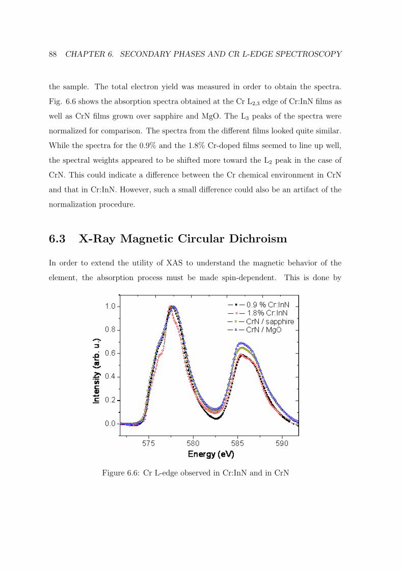
88 CHAPTER 6. SECONDARY PHASES AND CR L-EDGE SPECTROSCOPY
the sample. The total electron yield was measured in order to obtain the spectra.
Fig. 6.6 shows the absorption spectra obtained at the Cr L2,3 edge of Cr:InN films as
well as CrN films grown over sapphire and MgO. The L3 peaks of the spectra were
normalized for comparison. The spectra from the different films looked quite similar.
While the spectra for the 0.9% and the 1.8% Cr-doped films seemed to line up well,
the spectral weights appeared to be shifted more toward the L2 peak in the case of
CrN. This could indicate a difference between the Cr chemical environment in CrN
and that in Cr:InN. However, such a small difference could also be an artifact of the
normalization procedure.
6.3 X-Ray Magnetic Circular Dichroism
In order to extend the utility of XAS to understand the magnetic behavior of the
element, the absorption process must be made spin-dependent. This is done by
Figure 6.6: Cr L-edge observed in Cr:InN and in CrN
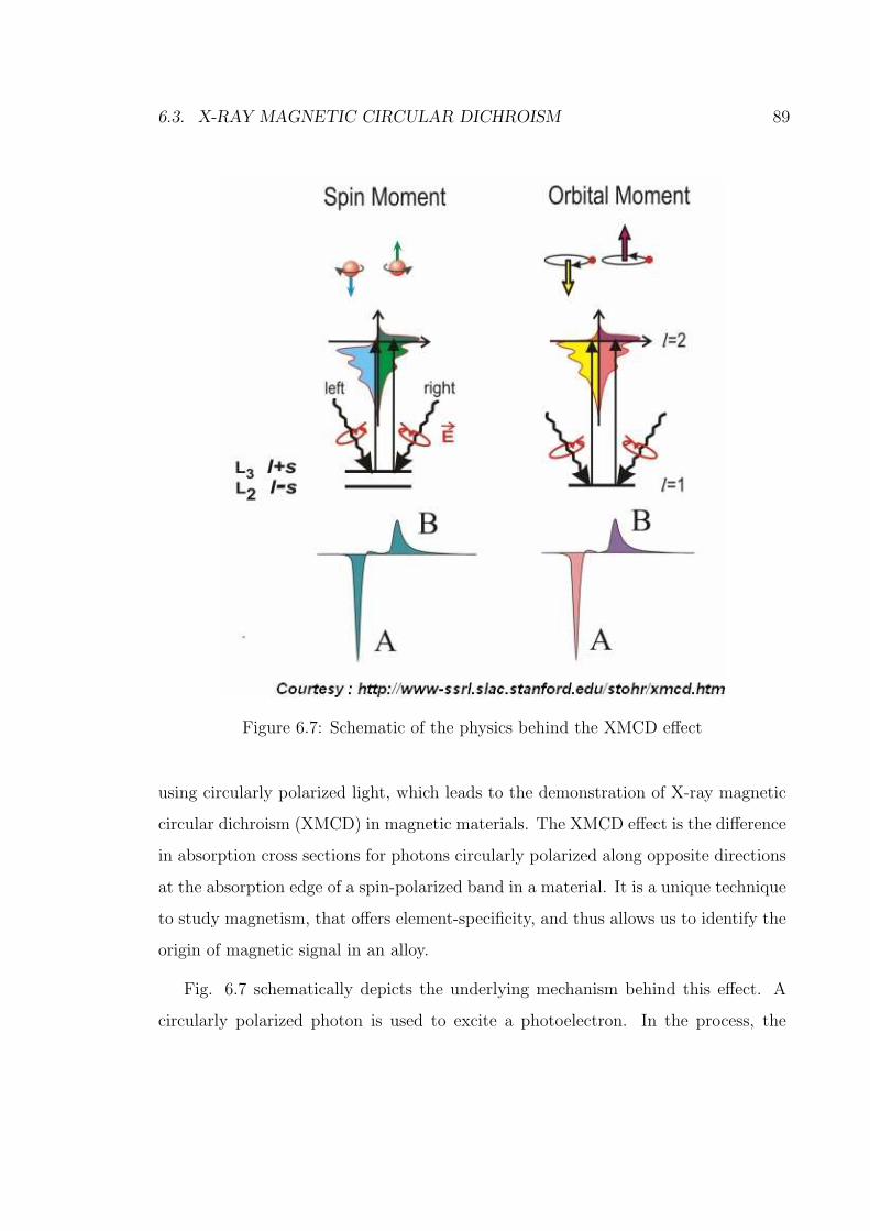
6.3. X-RAY MAGNETIC CIRCULAR DICHROISM 89
Figure 6.7: Schematic of the physics behind the XMCD effect
using circularly polarized light, which leads to the demonstration of X-ray magnetic
circular dichroism (XMCD) in magnetic materials. The XMCD effect is the difference
in absorption cross sections for photons circularly polarized along opposite directions
at the absorption edge of a spin-polarized band in a material. It is a unique technique
to study magnetism, that offers element-specificity, and thus allows us to identify the
origin of magnetic signal in an alloy.
Fig. 6.7 schematically depicts the underlying mechanism behind this effect. A
circularly polarized photon is used to excite a photoelectron. In the process, the
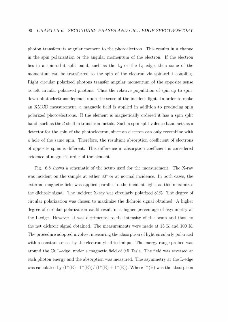
90 CHAPTER 6. SECONDARY PHASES AND CR L-EDGE SPECTROSCOPY
photon transfers its angular moment to the photoelectron. This results in a change
in the spin polarization or the angular momentum of the electron. If the electron
lies in a spin-orbit split band, such as the L2 or the L3 edge, then some of the
momentum can be transferred to the spin of the electron via spin-orbit coupling.
Right circular polarized photons transfer angular momentum of the opposite sense
as left circular polarized photons. Thus the relative population of spin-up to spin-
down photoelectrons depends upon the sense of the incident light. In order to make
an XMCD measurement, a magnetic field is applied in addition to producing spin
polarized photoelectrons. If the element is magnetically ordered it has a spin split
band, such as the d-shell in transition metals. Such a spin-split valence band acts as a
detector for the spin of the photoelectron, since an electron can only recombine with
a hole of the same spin. Therefore, the resultant absorption coefficient of electrons
of opposite spins is different. This difference in absorption coefficient is considered
evidence of magnetic order of the element.
Fig. 6.8 shows a schematic of the setup used for the measurement. The X-ray
was incident on the sample at either 30◦ or at normal incidence. In both cases, the
external magnetic field was applied parallel to the incident light, as this maximizes
the dichroic signal. The incident X-ray was circularly polarized 81%. The degree of
circular polarization was chosen to maximize the dichroic signal obtained. A higher
degree of circular polarization could result in a higher percentage of asymmetry at
the L-edge. However, it was detrimental to the intensity of the beam and thus, to
the net dichroic signal obtained. The measurements were made at 15 K and 100 K.
The procedure adopted involved measuring the absorption of light circularly polarized
with a constant sense, by the electron yield technique. The energy range probed was
around the Cr L-edge, under a magnetic field of 0.5 Tesla. The field was reversed at
each photon energy and the absorption was measured. The asymmetry at the L-edge
was calculated by (I+(E) - I−(E))/ (I+(E) + I−(E)). Where I+(E) was the absorption

6.3. X-RAY MAGNETIC CIRCULAR DICHROISM 91
Figure 6.8: XMCD measurement setup
with the photon helicity parallel to the magnetic field at photon energy E, while I−(E)
was that with the helicity antiparallel to the field. Similar measurements were made
with the incident photons circularly polarized along the opposite sense. This was
done in order to check if the dichroic signal changed sign, thereby confirming that
the observed asymmetry was in fact real, and not a measurement artifact.
Figure 6.9 shows the dichroism observed at the Cr L-edge in the 0.9% Cr-doped
InN at 15K, under normal incidence. A small but clear dichroism was observed at
the L-edge, and the sign of the signal reversed upon changing the sense of the circular
polarization of the incident X-ray. This was evidence that the Cr in Cr:InN did exhibit
long range magnetic order. One point to note was the magnitude of the dichroic signal.
The asymmetry was only 0.15% of the edge jump, which was very small given that the
normalized moment per Cr in this sample was computed to be about 5 µB. Sum rules
normally relate the spin and orbital momentum quantitatively to a linear combination

92 CHAPTER 6. SECONDARY PHASES AND CR L-EDGE SPECTROSCOPY
Figure 6.9: Dichroism at the Cr L-edge in Cr-doped InN
of the L2 and L3 branches of the dichroic signals [70]. These however, are less effective
in the case of early 3d elements [71] such as Cr, mainly because of mixing of the
L3,2 branches which makes deconvolution of the two branches difficult. Therefore
the spin moment per Cr was not computed from the dichroic signal. Nevertheless,
it could be concluded qualitatively, that the Cr moment suggested by XMCD was
significantly lower than that observed by SQUID. This discrepancy suggests that
some of the magnetic signal observed could probably be attributed to polarization
of the In or N. However, no XMCD signal was observed at the In L-edge. Similar
observation has been made with Co-doped ZnO [19], and has been attributed to the
magnetic polarization of the semiconductor lattice. The caveat is that while, XMCD
is sensitive only to the top 2 nm of the film, SIMS data for this film suggested that
it was terminated with a 1 nm layer of Nitrogen. This could be the reason for the
small dichroic signal observed.

6.3. X-RAY MAGNETIC CIRCULAR DICHROISM 93
Dichroism was observed as high as 100 K. Fig. 6.10 shows the spectrum taken at
100 K, with the data smoothed out for improved clarity. The signal was significantly
smaller due to the temperature dependence of the magnetization. The observation
dichroism under an applied field of 5 kOe at 100 K ruled out paramagnetic behavior,
indicating either ferromagnetic order or spin-glass behavior that was robust up to
high temperatures.
While dichroism was observed at the Cr L-edge in several Cr-doped InN films,
neither of the CrN films showed any dichroism. This, in addition to the XAS spectra
was taken to be evidence that CrN inclusions were probably not responsible for the
magnetic behavior of Cr:InN. To compare the behavior of Cr-doped InN to reports in
the literature, the absorption spectrum appears similar to that exhibited by CrO2 [72].
However, the dichroic signal is different, with CrO2 exhibiting a stronger multiplet
structure. Furthermore, a large fraction of the negative weight of the asymmetry is
observed at the low energy side of the L3 edge in Cr-doped InN, whereas it is right at
the L3 edge in CrO2. The dichroism is more similar to that exhibited by chalcogenides
CuCr2Se4 [73]. Earlier work on CoCrTa and CoCrPt indicate that the two features
with opposite sign in the asymmetry for the Cr L3 edge are not observed in metallic
Cr [74]. Thus the electronic and magnetic configuration of Cr in Cr:InN is most not
metallic in nature either, but similar to that in chalcogenides.
In summary, the role of secondary phases and the origin of the magnetic behavior
of Cr-doped InN was probed in greater detail using both SQUID magnetometry and
spectroscopic techniques. CrN deposited over MgO had relatively good crystalline
quality and behaved like a paramagnet. On the other hand, CrN grown on sapphire
was deposited in the form of grains and exhibited similar magnetic behavior to that
of Cr:InN. While there was a difference between the shape of the Cr L-edge absorp-
tion spectrum of Cr:InN and that of CrN, this could not conclusively be considered
evidence that the chemical environment of Cr was different in the two compounds.

94 CHAPTER 6. SECONDARY PHASES AND CR L-EDGE SPECTROSCOPY
Figure 6.10: Temperature dependence of dichroism observed at the Cr L-edge inCr-doped InN. The spectrum taken at 100 K has been smoothed out.

6.3. X-RAY MAGNETIC CIRCULAR DICHROISM 95
However, a dichroism was observed at the Cr L-edge in Cr:InN up to 100 K,
indicating long range magnetic order, which was not observed in CrN. The magnitude
of the signal was very small compared to the large moment observed by SQUID. This
led us to conclude that it was possible that the InN matrix was partially polarized,
and that it contributed to the net magnetization.

Chapter 7
Conclusions
While dilute magnetic semiconductors could be a useful class of materials and as-
sume a crucial role in enabling the semiconductor spintronic devices, much remains
unanswered with regards to the mechanism of magnetism in these materials. Tra-
ditional III-V candidates such as GaMnAs and InMnAs, which are typically p-type,
have been studied in great detail. Optical as well as electrical measurements have
established carrier-mediated ferromagnetism in these materials. However, the highest
Tc obtained in these materials still remains under 200 K, making them undesirable for
technological applications. On the other hand, up and coming n-type candidates such
as doped GaN and ZnO seem to exhibit magnetic order at much higher temperatures.
However, with no solid theories explaining the observed properties such as magnetic
hysteresis in n-type materials, the origin of magnetism is still under debate.
In this work we have studied one such candidate - Cr and Mn doped InN. The
growth, structure and magnetism in Cr-doped InN was examined in detail. The films
were deposited by MBE, which is an ideal technique for growth of these materials
that need to be deposited under non-equilibrium conditions. C-plane sapphire sub-
strates were used, and thin GaN buffer layers, whose thickness was typically around
1000 A. Thereafter, InN films of thickness varying between 250 A and 1500 A were
96

97
deposited, followed by the Cr or Mn-doped layers, whose thickness was in the range
of 100-700 A. The growths were monitored in situ by reflection high energy electron
diffraction, which indicated a smooth 2-dimensional deposition. The films were of
reasonably good structural quality, as observed by a full width at half maximum of
0.1◦ rocking curve X-Ray Diffraction. Cr-doped films showed no signs of secondary
phase segregation, whereas Mn-doped films clearly exhibited segregation of Mn3N2.
Both Cr-doped films and nominally undoped films exhibited a very high n-type
carrier concentration, around 5.1019 - 1.1020 cm−3. The high carrier concentration is
expected to arise from defects in the crystal such as nitrogen vacancies and oxygen
inclusions. Cr-doped films showed n-type behavior as well. The films showed poor
mobility, under 100 cm2V−1s−1. This could be a result of the small thickness of the
films, which would lead to films with a high defect concentration. Further, since
the Cr-doped layers were deposited at low temperatures, they had poorer structural
quality, leading to the low mobilities. Photoluminescence revealed a band gap of 0.84
eV in both InN and Cr:InN.
Magnetic characterization of Cr:InN revealed a hysteresis up to room temperature,
with a rounded shape, and small coercivity. The remanence showed a steady drop
with increase in temperature. All this indicated long range magnetic order up to
room temperature. On the other hand, Mn:InN exhibited paramagnetic behavior,
showing a very weak hysteresis behavior, and a 1/T-like temperature dependence of
magnetism. This was attributed to secondary phase formation in this material. The
moment obtained per Cr atom was relatively large in Cr:InN, with one of the 0.9%
doped films exhibiting a moment as large as 5µB. Further, first evidence of spin
polarized transport was also seen in one of the Cr:InN samples doped with 1.8% Cr,
as a small anomalous Hall contribution.
Despite all this evidence indicating ferromagnetism, there were aspects of the
magnetic behavior that pointed towards frustrated or spin-glass like behavior. Field

98 CHAPTER 7. CONCLUSIONS
cooled vs.zero field cooled measurements showed different slopes for the FC and ZFC
traces. Further, the remanence showed irreversibility in it temperature dependence,
although it did not show any signs of relaxation with time. One potential secondary
phase that could produce this behavior, CrN was also studied. Although this material
exhibited magnetic behavior similar qualitatively to that of Cr:InN, X-ray absorption
spectroscopy showed a difference in the Cr L-edge between CrN and Cr:InN. Moreover,
a small dichroism was observed at the Cr L-edge up to 100 K, indicating magnetic
order of the Cr. This was not observed in CrN.
One interesting point about the magnetic behavior was the magnitude of the
saturated moment per Cr. While the moment obtained by SQUID in the 0.9% Cr-
doped InN film was relatively large (5 µB), the asymmetry relative to the edge jump
at the L-edge in this sample was only 0.15%. This would indicate a much smaller
atomic spin moment on the Cr than that measured by SQUID. This discrepancy in the
magnitudes of the moment on the Cr could be explained in part from an inflation in
the signal measured due to impurities, or reduction in the XMCD signal due to surface
contamination. However, this behavior was consistently observed in several samples,
and has also been seen in Gd:GaN [65]. Therefore, it is possible that polarization of
the lattice by the magnetic ions results contributes to the magnetic signal observed.
In summary, Cr:InN appears to be a frustrated system, exhibiting such properties
as thermomagnetic irreversibility. However, it shows magnetic order that is robust
with time, and is observed well above room temperature. Further, the high saturation
moment exhibited as well as first evidence seen of spin-polarized transport make this
and other similar n-type DMS materials potentially significant materials, both from
the point of view of understanding the magnetism, as well as for device applications.
Bibliography
[1] “Cramming more components onto integrated circuits”, Gordon Moore, Elec-
tronics, 38, (1965).
[2] S. Datta and B. Das, Appl. Phys. Lett. 56, 665667 (1990).
[3] G. Schmidt, D. Ferrand, L.W. Molenkamp, A.T. Filip, and B.J. Van Wees, Phys.
Rev.B 62, R4790 (2000).
[4] S. Methfessel and D. C. Mattis, in Magnetism, Magnetic Semiconductors, vol.
XVIII/1 of Encyclopedia of Physics, 389562 (1968).
[5] H. Ohno, D. Chiba, F. Matsukura, T. Omiya, E. Abe, T. Dietl, Y. Ohno, and
K. Ohtani, Nature, 408, p. 944 (2000).
[6] S. Koshihara, A. Oiwa, M. Hirasawa, S. Katsumoto, Y. Iye, C. Urano, H. Takagi,
and H. Munekata, Phys. Rev. Lett. 78, 4617 (1997).
[7] T. Kasuya and A. Yanase, Rev. Mod. Phys. 40, 684 (1968).
[8] H. Munekata, H. Ohno, S. Von Molnar, A. Segmuller, L. L. Chang, L. Esaki,
Phys. Rev. Lett. 63, 1849 (1989).
[9] T. Dietl, H. Ohno, F. Matsukura, J. Cibert, and D. Ferrand, Science 287, 1019
(2000).
99

100 BIBLIOGRAPHY
[10] M. Herbich, A. Twardowsky, D. Scalbert, A. Petrou , Phys. Rev.B 58, 7024
(1998).
[11] C. Zener, Phys. Rev. 81, p. 440 (1950); Phys. Rev. 83, p. 299 (1950).
[12] J. Furdyna, J. Appl. Phys. 64, R29 (1986).
[13] H. Ohno, A. Shen, F. Matsukura, A. Oiwa, A. Endo, S. Katsumoto, and Y. Iye,
Appl. Phys. Lett. 9 , p. 363 (1996).
[14] S. Dhar, O. Brandt, and K. Ploog, Appl. Phys. Lett. 86, 112504 (2005).
[15] N. Y. H. Hong, J. Sakai, and A. Hassini, Appl. Phys. Lett. 84, p. 26022604
(2004).
[16] S. B. Ogale et al, Phys. Rev. Lett. 91, p. 077205 (2003).
[17] ’Introduction to Solid State Physics’, C. Kittel (1996)
[18] Adam C. Durst, R. N. Bhatt, and P. A. Wolff, Phys. Rev. B, 65, p. 235205
(2002).
[19] J. M. D.Coey, M. Venkatesan, and C. B. Fitzgerald, Nature Mat. 4 p.173 (2005).
[20] V. Canella and J.A. Mydosh, Phys. Rev. B 6, p. 4220 (1972).
[21] S. Sonoda, S. Shimizu, T. Sasaki, T. Yamamoto, and H. Hori, J. Cryst. Growth
237, p. 13581362 (2002).
[22] M. Hashimoto, Y. K. Zhou, M. Kanamura, H. Asahi, Solid State Commun. 122,
p. 3739 (2002).
[23] S. Y. Wu et al, Appl. Phys. Lett. 82, p. 30473049 (2003).
[24] Y. Matsumoto, et al. Science 291,p. 854856 (2001).

BIBLIOGRAPHY 101
[25] S. R. Shinde, et al. Phys. Rev B 67, p. 115211 (2003).
[26] Z. J. Wang, J. K. Tang, L. D. Tung, W. L. Zhou, and L. Spinu, J. Appl. Phys.
93, p. 78707872 (2003).
[27] J. M. D. Coey, A. P. Douvalis, C. B. Fitzgerald, an M. Venkatesan, Appl. Phys.
Lett. 84, p. 13321334 (2004).
[28] H. Saeki, H. Tabata, and T. Kawai, Solid State Commun. 120, p.439443 (2001).
[29] S. J. Han et al, Appl.Phys. Lett. 83, p. 920922 (2003).
[30] K. Ueda, H. Tabata, and T. Kawai, Appl. Phys. Lett. 79, p. 988990 (2001).
[31] P. V. Radovanovic, and D. R. Gamelin, Phys. Rev. Lett. 91, p. 157202 (2003).
[32] S. N. Kale, et al, Appl. Phys. Lett. 83, p. 21002102 (2003).
[33] J. Philip, N. Theodoropolou, G. Berera, J. S. Moodera, and B. Satpati, Appl.
Phys. Lett. 85, p. 777 (2004).
[34] P. P. Chen, H. Makino, and T. Yao, Sol. State Comm., 130, p. 25 (2004).
[35] R. Rajaram, A. Ney, G. Solomon, J. S. Harris, Jr., R. F. C. Farrow, and S. S. P.
Parkin, Appl. Phys. Lett. 87, 172511 (2005).
[36] P. A. Anderson, R. J. Kinsey, S. M. Durbin, A. Markwitz, V. J. Kennedy, A.
Asadov, W. Gao, and R. J. Reeves, J.Appl. Phys. 98, 043903 (2005).
[37] A. Ney, R. Rajaram, R. F. C. Farrow, J. S. Harris, Jr., and S. S. P. Parkin, J.
Superconductivity 18, 41 (2005).
[38] A. Ney, R. Rajaram, E. Arenholz, J. S. Harris, Jr.,M. Samant, R. F. C. Farrow,
and S. S. P. Parkin, J. Mag. Mag. Mat. 300, p. 1-7 (2006).

102 BIBLIOGRAPHY
[39] A. Zubrilov, in Properties of Advanced Semiconductor Materials GaN, AlN, InN,
BN, SiC, SiGe, M. E. Levinshtein, S. L. Rumyantsev, and M. S. Shur, eds. (Wiley,
New York, 2001), pp. 4966.
[40] Q. X. Guo, N. Nisho, H. Ogawa, and A. Yoshida, Jpn. J. Appl. Phys. Part 2 38,
L490 (1999).
[41] B. E. Foutz, S. K. OLeary, M. S. Shur, and L. F. Eastman, J. Appl. Phys. 85,
7727 (1999).
[42] A. G. Bhuyian, A. Hashimoto, and A. Yamamoto, J. Appl. Phys. 94, 2779 (2003).
[43] Chinkyo Kim, I. K. Robinson, Jaemin Myoung, Kyu-Hwan Shim, and Kyekyoon
Kim J. Appl. Phys. 85, 4040 (1999).
[44] T. W. Kima, D. U. Lee, Haengdang-dong, Seongdong-gu, H. S. Lee, J. Y. Lee,
Gusung-dong, Yusung-ku, J. Appl. Phys. 96, p. 7118 (2004).
[45] T. Yamaguchi, Y. Saito, K. Kano, T. Araki, N. Teraguchi, A. Suzuki, and Y.
Nanishi, phys. stat. sol. (b) 228, 17 (2001).
[46] Maria Losurdo, Pio Capezzuto, Giovanni Bruno, Gon Namkoong, W. Alan
Doolittle, and April S. Brown J. Appl. Phys. 91, 2508 (2002).
[47] W. E. Hoke, P. J. Lemonias, and D. G. Weir, J. Cryst. Growth 111, 1024 (1991).
[48] Yasushi Nanishi, Yoshiki Saito and Tomohiro Yamaguchi, Jpn. J. Appl. Phys.,
42, pp. 25492559 (2003).
[49] G. J. Whaley, and P. I. Cohen, J. Vac. Sci. Tech. B, 6, p. 625 (1988).
[50] P. R. Berger, K. Chang, P. K. Bhattacharya, and J. Singh, J. Vac. Sci. Tech. B,
5, p. 1162 (1987).

BIBLIOGRAPHY 103
[51] Gon Namkoonga, W. Alan Doolittle, April S. Brown, Maria Losurdoc, Maria M.
Giangregorioc, Giovanni Brunoc, J. Cryst. Growth, 252, p. 159166 (2003).
[52] L. Bellaiche, S.H. Wei, and Alex Zunger, Phys. Rev. B 56, 13872 (1997).
[53] M. Hashimoto, S. Emura, H. Tanaka, T. Honma, N. Umesaki, S. Hasegawa, and
H. Asahi, J. App. Phys. 100, 103907 (2006).
[54] B. Jahnen, M. Albrecht, W. Dorsch , S. Christiansen, H. P. Strunk, D. Hanser,
and Robert F. Davis, Mat. Res. Soc. Internet J. Niride Semicond. Res. 3, p. 39
(1998).
[55] T. L. Tansley and C. P. Foley, J. Appl. Phys. 59, p. 3241 (1986).
[56] V. Y. Davydov et al., Phys. Status Solidi B 230, R4 (2002).
[57] J. Wu, W. Walukiewicz, K. M. Yu, J. W. Ager III, E. E. Haller, H. Lu, W. J.
Schaff, Y. Saito, and Y. Nanishi, Appl. Phys. Lett. 80, p. 3967 (2002).
[58] T. Matsuoka, H. Okamoto, M. Nakao, H. Harima, and E. Kurimoto, Appl. Phys.
Lett. 81, p. 1246 (2002).
[59] Yoshiki Saito, Nobuaki Teraguchi, Akira Suzuki, Tsutomu Araki, and Yasushi
Nanishi, Jpn. J. Appl. Phys., 40, pp. L 91L 93 (2001).
[60] Craig H. Swartz, Randy P. Tomkins, Thomas H. Myers, Hai Lu, and William J.
Schaff, phys. stat. sol. (c) 7, p. 2250 (2005).
[61] M. L. Reed, N. A. El-Masry, H. H. Stadelmaier, M. K. Ritums, M. J. Reed, C.
A. Parker, J. C. Roberts, and S. M. Bedair, Appl. Phys. Lett. 79, p. 3473 (2001).
[62] S. Dhar, O. Brandt, A. Trampert, L. Dweritz, K. J. Friedland, K. H. Ploog, J.
Keller, B. Beschoten, and G. Gntherodt, Appl. Phys. Lett. 82, p. 2077 (2003).

104 BIBLIOGRAPHY
[63] H. Yang, H. Al-Birthen, E. Trifan, D. C. Ingram, and A. Smith, J. Appl. Phys.
91, 1053 (2002).
[64] L. M. Corliss, N. Elliot, and J. M. Hastings, Phys. Rev. 117, 929 (1960).
[65] A. Ney, R. Rajaram, T. Kammermeier, E. Manuel, V. Ney, S. Dhar, E. Arenholz,
F. Wilhelm, A. Rogalev, K. H. Ploog, and S. S. P. Parkin, submitted.
[66] T. Jungwirth, Qian Niu, and A. H. MacDonald, Phys. Rev. Lett., 88, p. 207208
(2002).
[67] A. Ney, R. Rajaram, S. S. P. Parkin, T. Kammermeier, and S. Dhar, Appl. Phys.
Lett. 89, p. 112504 (2006).
[68] S. Dhar, O. Brandt, A. Trampert, K. J. Friedland, Y. J. Sun, and K. H. Ploog,
Phys. Rev. B 67, 165205 (2003).
[69] G. T. Thaler, M. E. Overberg, B. Gila, R. Frazier, C. R. Abernathy, S. J. Pearton,
J. S. Lee, S. Y. Lee, Y. D. Park, Z. G. Khim, J. Kim, and F. Ren, Appl. Phys.
Lett., 80, p. 3964 (2003).
[70] B. T. Thole, P. Carra, F. Sette, and G. van der Laan, Phys. Rev. Lett. 68, p.
1943 (1992).
[71] A. Scherz, H.Wende, C. Sorg, K. Baberschke, J. Minar, D. Benea, and H. Ebert,
Physica Scripta. Vol. T 115, p. 586588 (2005).
[72] E. Goering, A. Bayer, S. Gold, G. Schutz, M. Rabe, U. Rudiger, G. Guntherodt,
Phys. Rev. Lett. 88, p. 207203 (2002).
[73] A. Kimura, J. Matsuno, J. Okabayashi, A. Fujimori, T. Shishidou, E. Kulatov,
T. Kanomata, Phys. Rev. B 63, p. 224420 (2001).

BIBLIOGRAPHY 105
[74] K. M. Kemner, Y. U. Idzerda, V.G. Harris, V. Chakarian, W. T. Elam, C. C.
Kao, E. Johnson, Y.C. Feng, D. E. Laughlin, C. T. Chen, K. B. Lee, J. C.
Lodder, J. Appl. Phys. 81, p. 1002 (1997).


![Oxides and nitrides as alternative plasmonic materials in ...aeb/pubs/Oxides and nitrides as... · Oxides and nitrides as alternative plasmonic materials in the optical range [Invited]](https://static.fdocuments.us/doc/165x107/5c78446609d3f2cb498ba301/oxides-and-nitrides-as-alternative-plasmonic-materials-in-aebpubsoxides-and.jpg)