Spectral Breathing and Its Mitigation in Digital ...
11
IEEE JOURNAL OF SOLID-STATE CIRCUITS, VOL. 56, NO. 10, OCTOBER 2021 3191 Spectral Breathing and Its Mitigation in Digital Fractional- N PLLs Enrique Alvarez-Fontecilla , Eslam Helal , Amr I. Eissa , and Ian Galton , Fellow, IEEE Abstract—Although digital phase-locked loops (PLLs) offer several advantages over their analog counterparts, they suffer from a major disadvantage that is rarely mentioned in pub- lished articles. The disadvantage, known as spectral breathing, is caused by component mismatches among the frequency control elements within a PLL’s digitally controlled oscillator (DCO). The mismatches introduce DCO frequency modulation nonlinearity which fluctuates and, therefore, causes erratic variations in the PLL’s measured phase noise spectrum as the DCO’s free-running frequency drifts. The phenomenon is called spectral breathing because the measured phase noise spectrum tends to slowly swell and contract over time as if taking breaths of air. During these breaths, the PLL’s phase noise often becomes severely degraded. This article presents an experimental demonstration of the spectral breathing phenomenon and its solution in a digital fractional- N PLL. The demonstrated solution is a multi-rate dynamic element matching technique and a mismatch-noise cancellation technique that together eliminate spectral breathing. Index Terms— Digital calibration, digitally controlled oscillator (DCO), digital phase-locked loop (PLL), frequency control element (FCE), frequency synthesis, inter-symbol interfer- ence (ISI), multi-rate dynamic element matching (MR-DEM), mismatch-noise cancellation (MNC), spectral breathing. I. I NTRODUCTION D IGITAL fractional- N phase-locked loops (PLLs) offer several advantages over analog PLLs, such as lower loop filter circuit area and better compatibility with highly scaled CMOS IC technology [1], [2]. However, unlike their analog counterparts, many digital PLLs suffer from a problem called spectral breathing which can significantly degrade phase noise performance. Spectral breathing is the result of nonlinear frequency mod- ulation from inevitable mismatches among the frequency con- trol elements (FCEs) in a PLL’s digitally controlled oscillator (DCO) [3]. Flicker noise, temperature variations, and supply voltage variations cause the DCO’s free-running frequency to drift over time, so different FCEs are exercised as the PLL adjusts the DCO’s input sequence to compensate for the drift. This causes the DCO’s frequency modulation nonlinearity to Manuscript received January 4, 2021; revised March 12, 2021 and April 18, 2021; accepted April 19, 2021. Date of publication May 12, 2021; date of current version September 24, 2021. This article was approved by Associate Editor Pietro Andreani. This work was supported by the National Science Foundation under Award 1617545. (Corresponding author: Enrique Alvarez-Fontecilla.) Enrique Alvarez-Fontecilla is with Analog Devices Inc., San Diego, CA 92128 USA (e-mail: [email protected]). Eslam Helal, Amr I. Eissa, and Ian Galton are with the Electrical and Computer Engineering Department, University of California, San Diego, La Jolla, CA 92092 USA. Color versions of one or more figures in this article are available at https://doi.org/10.1109/JSSC.2021.3074814. Digital Object Identifier 10.1109/JSSC.2021.3074814 vary and, therefore, the PLL’s measured phase noise spectrum to swell up from time to time as if taking breaths of air. The effect is particularly significant in the large percentage of digital PLLs that use a digital delta-sigma () modulator to oversample the fractional part of the DCO input. In such PLLs, the modulator drives a bank of FCEs called the fractional FCE bank and the integer part of the DCO input drives a separate bank of FCEs called the integer FCE bank. The fractional FCE bank’s FCEs are exercised many times per reference period because they are driven by the oversampling modulator. In contrast, the integer FCE bank’s FCEs are exercised at most once per reference period because they are driven directly by the integer part of the DCO’s input sequence. Accordingly, the error introduced by the integer FCE bank as a result of FCE mismatches is the main problem; it is spread over a much smaller Nyquist band than the corresponding error introduced by the fractional FCE bank, so much less of it is suppressed by the DCO’s lowpass frequency-to-phase filtering operation. Perhaps because the problem is not visible when mea- surements are restricted to time periods during which the integer FCE bank input bits do not change, it is seldom mentioned in the published literature. Nevertheless, in prac- tice the integer FCE bank input bits do change, at least over time periods of several seconds, because of the DCO’s free-running frequency drift, so the problem is significant in applications. To the knowledge of the authors, the phenomenon was first reported and explained, although not yet named, in [2]. The PLL presented in [2] uses the DCO frequency control method described above, which was already well-known and widely used at the time, so the authors of [2] were surprised to find that FCE mismatches caused the PLL’s measured phase noise spectrum to vary significantly over time. The reason the frequency control method described above is so widely used in digital PLLs is that it is very power-efficient because only the fractional part of the DCO input sequence is oversampled. Unfortunately, this very feature is what exac- erbates the spectral breathing problem. To date, only three solutions that mitigate spectral breathing yet retain this feature have been proposed [21]. An offline calibration technique is proposed in [4] and [5] to compensate for FCE mismatches, but the technique requires several minutes to complete. A dig- ital integer-boundary avoider circuit prior to the DCO is pro- posed in [3], yet the technique is only effective in cases where the integer FCE bank input bits change relatively infrequently. To the authors’ knowledge, the only published comprehensive solution is the combination of a multi-rate dynamic element 0018-9200 © 2021 IEEE. Personal use is permitted, but republication/redistribution requires IEEE permission. See https://www.ieee.org/publications/rights/index.html for more information. Authorized licensed use limited to: Univ of Calif San Diego. Downloaded on September 25,2021 at 01:33:36 UTC from IEEE Xplore. Restrictions apply.
Transcript of Spectral Breathing and Its Mitigation in Digital ...
IEEE JOURNAL OF SOLID-STATE CIRCUITS, VOL. 56, NO. 10, OCTOBER 2021 3191
Spectral Breathing and Its Mitigation in DigitalFractional-N PLLs
Enrique Alvarez-Fontecilla , Eslam Helal , Amr I. Eissa , and Ian Galton , Fellow, IEEE
Abstract— Although digital phase-locked loops (PLLs) offerseveral advantages over their analog counterparts, they sufferfrom a major disadvantage that is rarely mentioned in pub-lished articles. The disadvantage, known as spectral breathing,is caused by component mismatches among the frequency controlelements within a PLL’s digitally controlled oscillator (DCO). Themismatches introduce DCO frequency modulation nonlinearitywhich fluctuates and, therefore, causes erratic variations in thePLL’s measured phase noise spectrum as the DCO’s free-runningfrequency drifts. The phenomenon is called spectral breathingbecause the measured phase noise spectrum tends to slowlyswell and contract over time as if taking breaths of air. Duringthese breaths, the PLL’s phase noise often becomes severelydegraded. This article presents an experimental demonstrationof the spectral breathing phenomenon and its solution in a digitalfractional-N PLL. The demonstrated solution is a multi-ratedynamic element matching technique and a mismatch-noisecancellation technique that together eliminate spectral breathing.
Index Terms— Digital calibration, digitally controlled oscillator(DCO), digital phase-locked loop (PLL), frequency controlelement (FCE), frequency synthesis, inter-symbol interfer-ence (ISI), multi-rate dynamic element matching (MR-DEM),mismatch-noise cancellation (MNC), spectral breathing.
I. INTRODUCTION
D IGITAL fractional-N phase-locked loops (PLLs) offerseveral advantages over analog PLLs, such as lower loop
filter circuit area and better compatibility with highly scaledCMOS IC technology [1], [2]. However, unlike their analogcounterparts, many digital PLLs suffer from a problem calledspectral breathing which can significantly degrade phase noiseperformance.
Spectral breathing is the result of nonlinear frequency mod-ulation from inevitable mismatches among the frequency con-trol elements (FCEs) in a PLL’s digitally controlled oscillator(DCO) [3]. Flicker noise, temperature variations, and supplyvoltage variations cause the DCO’s free-running frequency todrift over time, so different FCEs are exercised as the PLLadjusts the DCO’s input sequence to compensate for the drift.This causes the DCO’s frequency modulation nonlinearity to
Manuscript received January 4, 2021; revised March 12, 2021 andApril 18, 2021; accepted April 19, 2021. Date of publication May 12,2021; date of current version September 24, 2021. This article was approvedby Associate Editor Pietro Andreani. This work was supported by theNational Science Foundation under Award 1617545. (Corresponding author:Enrique Alvarez-Fontecilla.)
Enrique Alvarez-Fontecilla is with Analog Devices Inc., San Diego,CA 92128 USA (e-mail: [email protected]).
Eslam Helal, Amr I. Eissa, and Ian Galton are with the Electrical andComputer Engineering Department, University of California, San Diego,La Jolla, CA 92092 USA.
Color versions of one or more figures in this article are available athttps://doi.org/10.1109/JSSC.2021.3074814.
Digital Object Identifier 10.1109/JSSC.2021.3074814
vary and, therefore, the PLL’s measured phase noise spectrumto swell up from time to time as if taking breaths of air.
The effect is particularly significant in the large percentageof digital PLLs that use a digital delta-sigma (��) modulatorto oversample the fractional part of the DCO input. In suchPLLs, the �� modulator drives a bank of FCEs calledthe fractional FCE bank and the integer part of the DCOinput drives a separate bank of FCEs called the integer FCEbank. The fractional FCE bank’s FCEs are exercised manytimes per reference period because they are driven by theoversampling �� modulator. In contrast, the integer FCEbank’s FCEs are exercised at most once per reference periodbecause they are driven directly by the integer part of theDCO’s input sequence. Accordingly, the error introduced bythe integer FCE bank as a result of FCE mismatches is themain problem; it is spread over a much smaller Nyquist bandthan the corresponding error introduced by the fractional FCEbank, so much less of it is suppressed by the DCO’s lowpassfrequency-to-phase filtering operation.
Perhaps because the problem is not visible when mea-surements are restricted to time periods during which theinteger FCE bank input bits do not change, it is seldommentioned in the published literature. Nevertheless, in prac-tice the integer FCE bank input bits do change, at leastover time periods of several seconds, because of the DCO’sfree-running frequency drift, so the problem is significant inapplications.
To the knowledge of the authors, the phenomenon was firstreported and explained, although not yet named, in [2]. ThePLL presented in [2] uses the DCO frequency control methoddescribed above, which was already well-known and widelyused at the time, so the authors of [2] were surprised to findthat FCE mismatches caused the PLL’s measured phase noisespectrum to vary significantly over time.
The reason the frequency control method described above isso widely used in digital PLLs is that it is very power-efficientbecause only the fractional part of the DCO input sequenceis oversampled. Unfortunately, this very feature is what exac-erbates the spectral breathing problem. To date, only threesolutions that mitigate spectral breathing yet retain this featurehave been proposed [21]. An offline calibration technique isproposed in [4] and [5] to compensate for FCE mismatches,but the technique requires several minutes to complete. A dig-ital integer-boundary avoider circuit prior to the DCO is pro-posed in [3], yet the technique is only effective in cases wherethe integer FCE bank input bits change relatively infrequently.To the authors’ knowledge, the only published comprehensivesolution is the combination of a multi-rate dynamic element
0018-9200 © 2021 IEEE. Personal use is permitted, but republication/redistribution requires IEEE permission.See https://www.ieee.org/publications/rights/index.html for more information.
Authorized licensed use limited to: Univ of Calif San Diego. Downloaded on September 25,2021 at 01:33:36 UTC from IEEE Xplore. Restrictions apply.

3192 IEEE JOURNAL OF SOLID-STATE CIRCUITS, VOL. 56, NO. 10, OCTOBER 2021
matching (MR-DEM) technique and a mismatch-noise cancel-lation (MNC) technique [21].
This article presents a fractional-N digital PLL IC thatincorporates the MR-DEM and MNC techniques to avoid spec-tral breathing. In addition to providing the first experimentaldemonstration of the techniques proposed in [21], it presentsimplementation details, refinements, and practical observationsthat are not presented in [21].
II. BACKGROUND INFORMATION
A. Conventional DCO Frequency Control Techniques
Most fractional-N digital PLLs have the general structureshown in Fig. 1(a), which consists of a phase-error-to-digitalconverter (PEDC), a digital loop filter (DLF), and a DCO.The PLL’s input, vref(t), is generated by a reference oscillatornot shown in the figure and the PLL’s output, vPLL(t), ideallyis periodic with frequency fPLL = (N + α) fref , where fref
is the reference oscillator frequency, N is a positive integer,and α is a fractional value. The PEDC generates an fref -ratesequence of the form −θPLL[n] + ep[n], where θPLL[n] is thePLL’s phase error and ep[n] represents the combined effect ofall other errors. The PEDC output is filtered by the DLF, andthe DLF output, d[n], controls the DCO frequency.
The DCO’s instantaneous frequency, fDCO(t), can be writtenas a fixed offset frequency plus ftune(t), where ftune(t) dependson the states of the DCO’s FCEs. Ideally, ftune(t) = d[nt ],where nt = n over the nth period of the fref -rate clockthat updates d[n], so nt is a continuous-time function thattakes on values n = 0, 1, 2, 3, . . . as t increases. If d[n]is represented as a b-bit two’s complement code sequenceand its least-significant bit (LSB) represents a frequency stepof �, then, d[nt ] = (−2b−1db−1[nt ] + 2b−2db−2[nt ] + . . . +20d0[nt ])�, where di [nt ] is the i th bit of the d[nt ] codefor i = 0, 1, . . . , b − 1. In principle, the DCO could beimplemented with b FCEs, where the i th FCE increasesor decreases fDCO(t) by 2i� whenever the FCE’s input bitchanges from 0 to 1 or 1 to 0, respectively. In this case, theinput to the i th FCE would be di [nt ] for i = 0, 1, . . . , b − 2,and 1 − di[nt ] for i = b − 1. Unfortunately, in most PLLs thiswould require FCEs with impractically small frequency steps.
Fig. 1(b) shows an example configuration of a DCO controltechnique that is widely used to circumvent this problem [1].In this example, the minimum practical FCE frequency stepis �min = 28�, and d[n] is decomposed into an integer part,dI [n], that takes on values that are multiples of �min, and afractional part, dF [n], that takes on values in the range {0, �,2�, . . . ,�min–�}. The dI [n] sequence drives an integer FCEbank directly. The dF [n] sequence is oversampled at a rateof ffast > fref and re-quantized by a digital �� modulator.The �� modulator output is converted to a thermometer codethat drives a fractional FCE bank which consists of fourFCEs, each with a frequency step of �min. Thus, ftune(t) isequal to d[nt ] plus ffast-rate highpass-shaped �� modulatorquantization error that is lowpass filtered by the DCO.
Ideally, the contribution to fDCO(t) from the i th FCE instan-taneously increases or decreases by �i when the FCE’s inputbit changes from 0 to 1 or 1 to 0, respectively, where �i is the
Fig. 1. (a) General form of a digital fractional-N PLL, (b) conventionalDCO control technique, and (c) illustration of the effects of non-ideal FCEbehavior on the PLL’s phase noise spectrum.
FCE’s nominal frequency step. In practice, non-ideal circuitbehavior causes the FCE’s frequency transitions to be non-instantaneous, and component mismatches cause its frequencystep to deviate somewhat from �i as illustrated in Fig. 1(c).These nonidealities introduce input-code-dependent DCO fre-quency modulation nonlinearity. As illustrated in Fig. 1(c),this causes the PLL’s phase noise spectrum to vary overtime as the DCO’s free-running frequency, and, hence, dI [n],drift [21].
In most low-noise PLLs that generate unmodulated outputtones, the short-term variation of d[n] is much less than �min.In such cases, the PLL output frequency can be tuned suchthat d[n] is far enough from an integer boundary that dI [n]initially remains constant. To the extent that this conditionpersists over time, the integer FCE bank does not introducedynamic error. However, flicker noise, temperature variations,and supply voltage variations inevitably cause the DCO’s free-running frequency to drift, and the PLL responds by adjustingd[n] to compensate for the drift. Eventually, this causes d[n]to get close enough to an integer boundary that dI [n] beginsto toggle, thereby causing the spectral breathing problem.Typically, such spectral breathing events occur at time intervalsranging from a few seconds to a few minutes.
Even if the DCO’s free-running frequency drift couldsomehow be avoided, preventing the integer FCE bank fromintroducing dynamic error by avoiding PLL output frequenciesfor which dI [n] toggles would not be practical in most appli-cations because it would arbitrarily prohibit the use of severalPLL output frequency bands. Moreover, in PLLs designed togenerate frequency or phase-modulated output waveforms, theshort-term variation of d[n] typically exceeds �min, in whichcase the integer FCE bank continuously introduces dynamicerror and severely degrades the PLL’s phase noise.
Authorized licensed use limited to: Univ of Calif San Diego. Downloaded on September 25,2021 at 01:33:36 UTC from IEEE Xplore. Restrictions apply.

ALVAREZ-FONTECILLA et al.: SPECTRAL BREATHING AND ITS MITIGATION IN DIGITAL FRACTIONAL-N PLLs 3193
Fig. 2. (a) Block diagram of a digital fractional-N PLL with the MR-DEMand MNC techniques and (b) MR-DEM technique details.
One solution is to apply DEM clocked at the �� modulatoroutput rate to all the DCO’s FCEs. This causes all error fromFCE mismatches to be free of nonlinear distortion and shapedto high-enough frequencies that it is largely suppressed bythe DCO. Unfortunately, the solution is prohibitively power-hungry because of the high sample rate, and having so manyrapidly toggling digital lines routed in close proximity to theDCO’s tank tends to couple noise and spurious tones into theDCO output.
A somewhat lower-power, but only partial solution is to havea single FCE bank driven by the output of an oversampling�� modulator with input d[n] rather than just dF [n] [16].While this option does not cause error from FCE mismatchesto be free of nonlinear distortion or shaped to high frequencies,it does spread the error over a larger Nyquist band so that moreof it gets suppressed by the DCO. Hence, it reduces, but doesnot eliminate, the spectral breathing problem, and it does notnecessarily avoid the problem of having a large number ofrapidly toggling digital lines routed in close proximity to theDCO’s tank.
The latter problem can be avoided by implementingthe DCO as an oversampling �� digital-to-analog con-verter (DAC) followed by a voltage-controlled oscillator(VCO) [9], [15], [17]–[20]. If the �� DAC implements DEM,then spectral breathing is avoided, but the problem of highpower consumption remains. Without DEM, as long as the ��DAC oversamples d[n] and not just dF [n], then the spectralbreathing problem is mitigated, but still not eliminated, for thereasons described above.
B. MR-DEM and MNC Techniques
Fig. 2(a) shows a high-level diagram of a digital fractional-N PLL that includes the MR-DEM and MNC techniques. Thesystem is similar to that shown in Fig. 1(a), except for theaddition of two digital blocks: an MR-DEM encoder that isbuilt into the DCO and an MNC logic block.
Fig. 3. Slow DEM encoder signal processing.
The MR-DEM encoder is based on the same principle asmismatch-shaping DEM encoders [6]. The idea is to shuffle theerror introduced by FCE mismatches, so that ftune(t) equals ascaled version of d[nt ] plus additive highpass-shaped error thatdepends on pseudorandom digital sequences that are known tothe system because they are generated within the MR-DEMencoder. This additive error has both fref -rate and ffast-ratecomponents. Most of the fref -rate error component in ftune(t)is cancelled by the MNC technique, which applies a least-mean-square (LMS)-like algorithm to compute digital coeffi-cients with which it forms a correction sequence, eMNC[p],that is injected into the MR-DEM encoder. The ffast-rate errorcomponent is not cancelled by the MNC technique, but its highsample-rate in conjunction with its highpass spectral shapeensures that most of its contribution to the DCO’s phase noisegets suppressed by the DCO’s first-order lowpass frequency-modulation-to-phase-noise transfer function.
Fig. 2(b) shows the details of the MR-DEM techniquefor an example case where d[n] has 16 bits. It consists ofan MR-DEM encoder that comprises a slow DEM encoder,a second-order digital �� modulator, and a fast DEM encoder.The slow DEM encoder is a modified version of a con-ventional segmented DEM encoder, the details of which aredescribed shortly, and the fast DEM encoder is a conventionalnon-segmented DEM encoder. The slow DEM encoder isclocked by the fref -rate clock signal, clkref(t), whereas theMR-DEM encoder’s fractional path, which consists of thedigital �� modulator and the fast DEM encoder, is clockedby the ffast-rate clock signal, clkfast(t).
The signal processing details of the slow DEM encoder areshown in Fig. 3, where the � multiplication prior to the x f [n]output denotes that the LSB of x f [n] represents a frequencystep of �. The slow DEM encoder consists of 25 digitalswitching blocks (SBs), labeled Sk,r for k = 1, 2, . . . , 16 andr = 1, 2, . . . , 17. The shaded SBs are called segmenting SBs,whereas the remaining SBs are called non-segmenting SBs.The functional details of each SB type are also shown in Fig. 3,
Authorized licensed use limited to: Univ of Calif San Diego. Downloaded on September 25,2021 at 01:33:36 UTC from IEEE Xplore. Restrictions apply.

3194 IEEE JOURNAL OF SOLID-STATE CIRCUITS, VOL. 56, NO. 10, OCTOBER 2021
Fig. 4. (a) MNC logic signal processing, (b) sk,r [n] residue estimator signalprocessing, and (c) illustration of the MNC technique operation where pt = pover the pth period of clkfast(t).
where ck,r [n] is the input sequence of Sk,r . The outputs of eachsegmenting SB are ½(ck,1[n]–1–sk,1[n]) and 1+ sk,1[n], wheresk,1[n], called a switching sequence, is 0 when ck,1[n] is oddand ±1 otherwise. The outputs of each non-segmenting SBare ½(ck,r [n]–sk,r [n]) and ½(ck,r [n] + sk,r [n]), where sk,r [n]is 0 when ck,r [n] is even and ±1 otherwise. Each switchingsequence is zero-mean and has a highpass-shaped powerspectral density that peaks at fref /2.
As explained in [21], in the absence of the MNC techniquethe MR-DEM encoder would cause
ftune(t) ∼= d[nt ] + �∑k,r
δk,r sk,r [nt ]
+ pfast(t)�∑k,r
γk,r (t)(sk,r [nt − 1] − sk,r [nt ]) (1)
where δk,r and γk,r (t) are constant and 1/ ffast-periodic wave-forms, respectively, that depend only on FCE errors, andpfast(t) is a series of unit-amplitude, 1/ ffast-width pulses thatgo high whenever nt changes.1 As implied by (1), the MR-DEM technique causes ftune(t) to be a linear function ofd[nt ] at the expense of introducing two additive error terms.One of the error terms is caused by FCE static gain errors,i.e., mismatch-induced errors in the FCEs’ frequency step-sizes. The other error term is inter-symbol interference (ISI)
1The summation indices in (1) indicate the summation over all k and rvalues corresponding to the SBs within the slow DEM encoder.
Fig. 5. Adder-free slow DEM encoder implementation.
that results from non-instantaneous rise and fall frequencytransients of individual FCEs [21].
The details of the MNC logic are shown in Fig. 4(a).It consists of 25 sk,r [n] residue estimators that each computea correction sequence corresponding to one of the slow DEMencoder’s switching sequences, and an adder that combinesthese sequences to form eMNC[p]. As shown in Fig. 4(b), eachsk,r [n] residue estimator comprises two branches, one to com-pute the correction sequence associated with FCE static gainerror, and another to compute the correction sequence associ-ated with ISI error, hereafter referred to as the static-error andISI-error correction branches, respectively.
As indicated in Fig. 4, the MNC logic block’s output is
eMNC[p] = �∑k,r
ak,r [n]sk,r [n]
+ pfast(t)�∑k,r
bk,r [n](sk,r [n − 1] − sk,r [n]) (2)
where ak,r [n] and bk,r [n] are measures called MNC coef-ficients that correspond to δk,r and γk,r (t), respectively.As explained in [21], the MNC coefficients converge suchthat eMNC[p] is a sampled measure of the additive error termsin (1). As illustrated conceptually in Fig. 4(c), when injectedinto the DCO as shown in Fig. 2(b), eMNC[p] largely preventsthese terms from contributing to the DCO’s phase noise.
III. IMPLEMENTATION DETAILS
The MR-DEM and MNC techniques were implementedas modifications to the 6.5-GHz digital fractional-N PLLpresented in [4]. The PEDC is based on a second-order ��frequency-to-digital converter (FDC). The �� FDC is basedon a dual-mode ring oscillator (DMRO) and it incorporates theall-digital enhancements described in [7] in addition to a timeamplifier (TA) prior to the phase-frequency detector (PFD).The DLF consists of a loop gain multiplier, three single-poleIIR stages, and a proportional-integral stage. As the details of
Authorized licensed use limited to: Univ of Calif San Diego. Downloaded on September 25,2021 at 01:33:36 UTC from IEEE Xplore. Restrictions apply.

ALVAREZ-FONTECILLA et al.: SPECTRAL BREATHING AND ITS MITIGATION IN DIGITAL FRACTIONAL-N PLLs 3195
Fig. 6. MNC logic bit-level implementation.
the underlying PLL are explained in [4], only the additionalimplementation details relevant to the MR-DEM and MNCtechniques are presented here.
A. MR-DEM Encoder
The high-level details of the implemented MR-DEMencoder are identical to those shown in Fig. 2(b). The second-order digital �� modulator is implemented as an errorfeedback structure to reduce its hardware complexity [8].The fast DEM encoder is implemented as a 4-layer tree ofnon-segmenting SBs with first-order highpass-shaped switch-ing sequences [9], [10]. The slow DEM encoder is imple-mented as shown in Fig. 5. The SBs within the slow and fastDEM encoders are identical to the adder-free SBs describedin [11], except for a modification made in the slow DEMencoder’s SBs for them to accommodate both white and first-order highpass-shaped switching sequences.
It follows from Fig. 3 that the slow DEM encoder bottomoutput, x f [n], is given by
�
16∑k=9
216−ksk,1[n], (3)
which can be computed by combining the bottom outputsof S16,1, S15,1, . . . and S9,1 as indicated in Fig. 3. However,in this work, x f [n] is instead computed without using adders toreduce the block’s hardware complexity. As explained shortly,the LSB, c8,1-LSB[n], of the input to S8,1, c8,1[n], correspondsto a quantized version of dF [n], and its quantization erroris proportional to (3). The proposed slow DEM encoderarchitecture takes advantage of this property to generate x f [n]by simply combining the bits of the dF [n] and c8,1-LSB[n]sequences as indicated in Fig. 5.
Fig. 5 implies that
x f [n] = −28
(1 − c8,1-LSB[n]
�
)� + dF [n] (4)
and the SB signal processing operations shown in Fig. 3 implythat
c8,1[n] = 1
28
(c[n] + 1 − 28 −
16∑k=9
216−ksk,1[n])
�. (5)
As explained in [29], the segmenting SBs use negative-extra-LSB encoding, so c8,1-LSB[n] has a negative weight. Thiswith the segmenting SB details presented in [29] implies thatc8,1-LSB[n] is given by minus the right side of (5) with c[n]replaced by dF [n]/�, i.e.,
c8,1-LSB[n] = − 1
28
(dF [n]
�+ 1 − 28 −
16∑k=9
216−ksk,1[n])
�.
(6)
Substituting (6) into (4) yields (3) plus a −� offset. Thisoffset is not a problem in practice because it is suppressed bya zero-frequency zero in the PLL’s transfer function.
B. MNC Logic
The MNC logic implementation details are shown in Fig. 6.Each variable is represented in fixed-point, two’s complementformat, and its number of bits is specified via the notation{bI .bF }, where bI and bF are the numbers of integer andfractional bits, respectively. The braces and bF are omitted incases where bF = 0.
Each sk,r [n] residue estimator computes two sequences,ek,r-stat[n] and ek,r-ISI[n]. The ek,r-stat[n] sequences are com-bined to form eMNC-stat[n], which corresponds to the first
Authorized licensed use limited to: Univ of Calif San Diego. Downloaded on September 25,2021 at 01:33:36 UTC from IEEE Xplore. Restrictions apply.

3196 IEEE JOURNAL OF SOLID-STATE CIRCUITS, VOL. 56, NO. 10, OCTOBER 2021
Fig. 7. Integer and fractional FCE banks layout.
summation in (2), i.e., the part of eMNC[p] associated withFCE static gain errors. The ek,r-ISI[n] sequences are combinedand then multiplied by the unit-amplitude pulse sequence,pfast(t), to form eMNC-ISI[p], which corresponds to the secondsummation in (2), i.e., the part of eMNC[p] associated withFCE ISI errors. Although not shown in Fig. 6, eMNC-stat[n]and eMNC-ISI[p] are combined at the �� modulator’s inputin Fig. 2(b) to form eMNC[p].
As explained in [28], each sk,r [n] is a concatenation ofsequences of the form 1, 0, . . . , 0, −1, 0, . . . , 0 or −1,0, . . . , 0, 1, 0, . . . , 0. Thus, |sk,r [n]| ≤ 1 and |sk,r [n]−sk,r [n −1]| ≤ 2 for all n, and the running sum of sk,r [n] never exceeds1 or −1. However, after startup, the finite state machines thatgenerate the switching sequences do not necessarily start atthe beginning of their respective cycles, which could cause themagnitudes of the running sums of some switching sequencesto exceed 1. This issue is avoided by the inclusion of a±1 clipper within each sk,r [n] accumulator as shown in Fig. 6.
Each MNC coefficient within each sk,r [n] residue estimatoris the output of a 29-bit clipping accumulator. The 20 LSBsof the coefficients are dropped prior to their respective mul-tiplication by sk,r [n] and sk,r [n − 1] − sk,r [n], which reducespower consumption at the expense of reducing the accuracywith which eMNC[p] cancels the additive error terms in (1).The number of bits to drop was determined with the aid ofsimulations performed by the authors using a bit-accurate,event-driven, C-language, custom PLL simulator such that thecontribution to the PLL’s phase noise from the residual errorthat is left after MNC is applied is negligible.
The purpose of the clipping operations in the sk,r [n] residueestimators is to reduce the maximum MNC coefficient conver-gence time by preventing the accumulator magnitudes frombecoming unnecessarily large prior to convergence. Providedthe clipping bounds are larger than the magnitudes of theconverged MNC coefficients, they have no effect once theMNC coefficients converge. The clipper bounds of ±255 werechosen with the aid of behavioral simulations that consideredpessimistic FCE mismatches. None of the MNC coefficientmagnitudes were expected to exceed 128 after convergence,so the bounds of ±255 provide a considerable margin.
The Ka and Kb gains are restricted to powers of 2 so theimplementation of their respective multipliers only involves
bus-shifting. Consequently, as shown in Fig. 6, the MNC logicrequires no actual digital multipliers.
C. DCO FCE Banks
The DCO consists of a single-turn center-tapped inductor, across-coupled NMOS pair, a tail resonant tank [12], a triode-MOS tail source, and integer and fractional FCE banks. Theimplemented FCEs are of the type presented in [2], andthe minimum-size FCE has an equivalent frequency step of�min = 160 kHz at 6.5 GHz. The integer FCE bank compriseseight 32 ×�min FCEs and five pairs of 16×, 8×, 4×, 2× and1 × �min FCEs, whereas the fractional FCE bank comprises16 �min FCEs. All FCEs are implemented by connecting oneor more �min FCEs in parallel.
Both FCE banks are laid out as illustrated in Fig. 7,where the FCEs are indexed according to their respectivecontrol bits. Each FCE is driven by a flip-flop clocked byclkfast(t), followed by a buffer. The size of each buffer isscaled according to the number of parallel �min FCEs itdrives so as to minimize the systematic mismatches amongthe FCE frequency transients, and, hence, lower the errorcontribution from ISI. Behavioral simulations performed bythe authors in which estimates of the FCE frequency transientswere implemented suggest that for the specific FCE archi-tecture used, the contribution to the PLL’s phase noise fromthe MR-DEM technique’s ISI error component is much lesssignificant than that of the static gain error component. Thisobservation was experimentally validated, as demonstratedin Section IV.
As shown in Fig. 7, the ten largest FCEs of the integerFCE bank, FCEs 25–34, are split into two halves each,which are laid out in a common-centroid fashion to avoidthe FCE mismatches from being exacerbated. As explainedin Section II-B, the MNC technique cancels much of theerror that arises from FCE mismatches, but the larger theFCE mismatches, the larger the required dynamic range ofeMNC[p] and the larger the resulting output dynamic range ofthe MR-DEM encoder’s fractional path. A larger fractionalpath output dynamic range is undesirable in practice as itincreases the MR-DEM encoder’s power consumption, as wellas the number of control lines that need to be routed from the
Authorized licensed use limited to: Univ of Calif San Diego. Downloaded on September 25,2021 at 01:33:36 UTC from IEEE Xplore. Restrictions apply.
ALVAREZ-FONTECILLA et al.: SPECTRAL BREATHING AND ITS MITIGATION IN DIGITAL FRACTIONAL-N PLLs 3197
DCO control to the FCE banks’ drivers. Therefore, care wastaken with the layout to minimize FCE mismatches.
IV. MEASUREMENT RESULTS
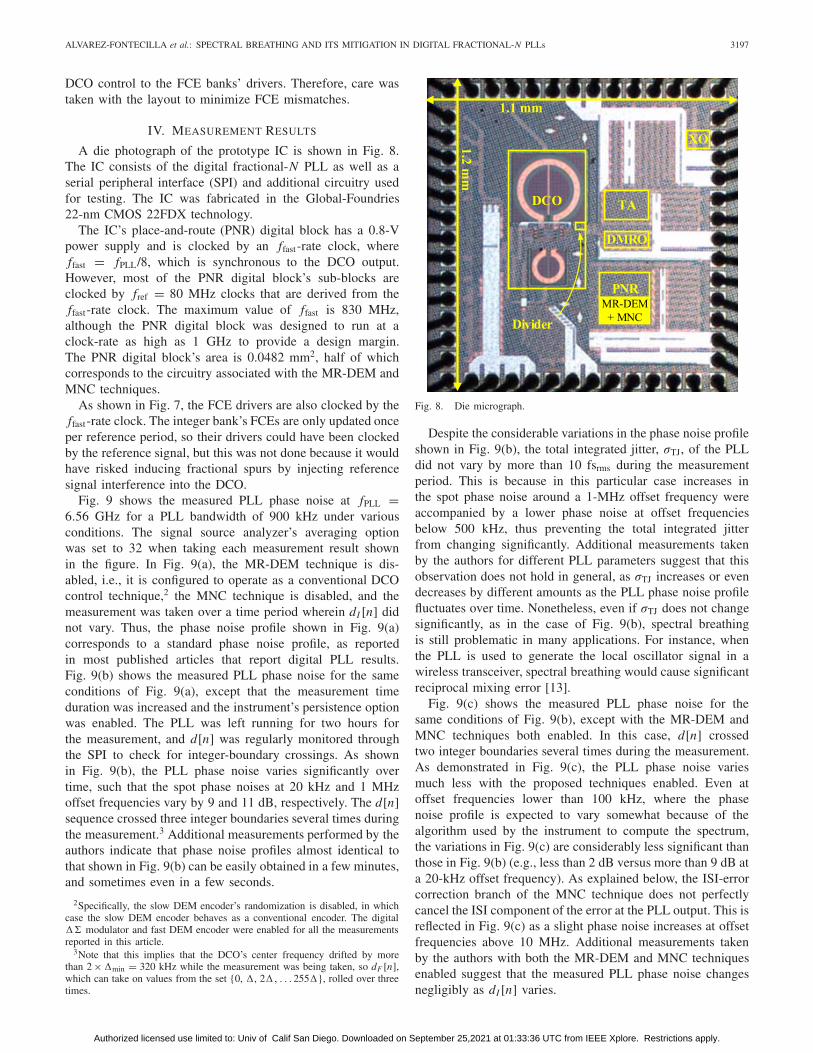
A die photograph of the prototype IC is shown in Fig. 8.The IC consists of the digital fractional-N PLL as well as aserial peripheral interface (SPI) and additional circuitry usedfor testing. The IC was fabricated in the Global-Foundries22-nm CMOS 22FDX technology.
The IC’s place-and-route (PNR) digital block has a 0.8-Vpower supply and is clocked by an ffast-rate clock, whereffast = fPLL/8, which is synchronous to the DCO output.However, most of the PNR digital block’s sub-blocks areclocked by fref = 80 MHz clocks that are derived from theffast-rate clock. The maximum value of ffast is 830 MHz,although the PNR digital block was designed to run at aclock-rate as high as 1 GHz to provide a design margin.The PNR digital block’s area is 0.0482 mm2, half of whichcorresponds to the circuitry associated with the MR-DEM andMNC techniques.
As shown in Fig. 7, the FCE drivers are also clocked by theffast-rate clock. The integer bank’s FCEs are only updated onceper reference period, so their drivers could have been clockedby the reference signal, but this was not done because it wouldhave risked inducing fractional spurs by injecting referencesignal interference into the DCO.
Fig. 9 shows the measured PLL phase noise at fPLL =6.56 GHz for a PLL bandwidth of 900 kHz under variousconditions. The signal source analyzer’s averaging optionwas set to 32 when taking each measurement result shownin the figure. In Fig. 9(a), the MR-DEM technique is dis-abled, i.e., it is configured to operate as a conventional DCOcontrol technique,2 the MNC technique is disabled, and themeasurement was taken over a time period wherein dI [n] didnot vary. Thus, the phase noise profile shown in Fig. 9(a)corresponds to a standard phase noise profile, as reportedin most published articles that report digital PLL results.Fig. 9(b) shows the measured PLL phase noise for the sameconditions of Fig. 9(a), except that the measurement timeduration was increased and the instrument’s persistence optionwas enabled. The PLL was left running for two hours forthe measurement, and d[n] was regularly monitored throughthe SPI to check for integer-boundary crossings. As shownin Fig. 9(b), the PLL phase noise varies significantly overtime, such that the spot phase noises at 20 kHz and 1 MHzoffset frequencies vary by 9 and 11 dB, respectively. The d[n]sequence crossed three integer boundaries several times duringthe measurement.3 Additional measurements performed by theauthors indicate that phase noise profiles almost identical tothat shown in Fig. 9(b) can be easily obtained in a few minutes,and sometimes even in a few seconds.
2Specifically, the slow DEM encoder’s randomization is disabled, in whichcase the slow DEM encoder behaves as a conventional encoder. The digital�� modulator and fast DEM encoder were enabled for all the measurementsreported in this article.
3Note that this implies that the DCO’s center frequency drifted by morethan 2 ×�min = 320 kHz while the measurement was being taken, so dF [n],which can take on values from the set {0, �, 2�, . . . 255�}, rolled over threetimes.
Fig. 8. Die micrograph.
Despite the considerable variations in the phase noise profileshown in Fig. 9(b), the total integrated jitter, σTJ, of the PLLdid not vary by more than 10 fsrms during the measurementperiod. This is because in this particular case increases inthe spot phase noise around a 1-MHz offset frequency wereaccompanied by a lower phase noise at offset frequenciesbelow 500 kHz, thus preventing the total integrated jitterfrom changing significantly. Additional measurements takenby the authors for different PLL parameters suggest that thisobservation does not hold in general, as σTJ increases or evendecreases by different amounts as the PLL phase noise profilefluctuates over time. Nonetheless, even if σTJ does not changesignificantly, as in the case of Fig. 9(b), spectral breathingis still problematic in many applications. For instance, whenthe PLL is used to generate the local oscillator signal in awireless transceiver, spectral breathing would cause significantreciprocal mixing error [13].
Fig. 9(c) shows the measured PLL phase noise for thesame conditions of Fig. 9(b), except with the MR-DEM andMNC techniques both enabled. In this case, d[n] crossedtwo integer boundaries several times during the measurement.As demonstrated in Fig. 9(c), the PLL phase noise variesmuch less with the proposed techniques enabled. Even atoffset frequencies lower than 100 kHz, where the phasenoise profile is expected to vary somewhat because of thealgorithm used by the instrument to compute the spectrum,the variations in Fig. 9(c) are considerably less significant thanthose in Fig. 9(b) (e.g., less than 2 dB versus more than 9 dB ata 20-kHz offset frequency). As explained below, the ISI-errorcorrection branch of the MNC technique does not perfectlycancel the ISI component of the error at the PLL output. This isreflected in Fig. 9(c) as a slight phase noise increases at offsetfrequencies above 10 MHz. Additional measurements takenby the authors with both the MR-DEM and MNC techniquesenabled suggest that the measured PLL phase noise changesnegligibly as dI [n] varies.
Authorized licensed use limited to: Univ of Calif San Diego. Downloaded on September 25,2021 at 01:33:36 UTC from IEEE Xplore. Restrictions apply.

3198 IEEE JOURNAL OF SOLID-STATE CIRCUITS, VOL. 56, NO. 10, OCTOBER 2021
Fig. 9. Measured PLL phase noise at fPLL = 6.56 GHz for (a) conventional DCO control technique with constant dI [n], (b) conventional DCO controltechnique and persistence enabled for 2 hrs, (c) MR-DEM and MNC enabled and persistence enabled for 2 hrs, and (d) MR-DEM disabled, MNC enabledwith coefficients frozen after convergence, and persistence enabled for 2 hrs.
Fig. 9(d) shows the measured PLL phase noise for the sameconditions of Fig. 9(c), except that the MR-DEM techniquewas disabled and the MNC technique’s coefficients werefrozen after convergence but prior to the measurement. In thiscase, d[n] crossed two integer boundaries several times duringthe measurement. The phase noise profile shown in Fig. 9(d)is similar to that shown in Fig. 9(c), except for slightly largervariations at offset frequencies below 200 kHz and at a 1-MHzoffset frequency, and the phase noise at offset frequenciesabove 10 MHz which does not exhibit the excess noise shownin Fig. 9(c). The increase in phase noise variation at lowoffset frequencies in Fig. 9(d) compared to Fig. 9(c) happensbecause MNC coefficient noise gets sampled, and, hence,locked in when the MNC coefficients are frozen. Hence, in thisconfiguration, the PLL’s performance is expected to be similarto that of the PLL without the MR-DEM and MNC techniquesenabled but with considerably smaller FCE mismatches.
The phase noise profile shown in Fig. 9(d) was obtained bysetting the MNC loop gains, Ka and Kb in Fig. 4(b), to 2−7 and2−8, respectively. Unfortunately, these are the minimum values
of Ka and Kb supported by this design, although it would havebeen simple to make the design support smaller values. Hadsmaller values of Ka and Kb been used, it is expected thatless “residual” spectral breathing would have occurred.
Fig. 10 shows the measured PLL phase noise at fPLL =6.56 GHz with the signal source analyzer’s averaging optionset to 32 and different combinations of the proposed tech-niques enabled and disabled. The PLL bandwidth was set to900 kHz in each case. Fig. 10(a) shows the effect on thePLL phase noise of the MR-DEM technique in the absence ofMNC compared to the baseline case of Fig. 9(a). As shownin the figure, the spot phase noise increases by up to 11.5 dBcompared to the case of Fig. 9(a), whereas σTJ from 10 kHzto 80 MHz increases from 176 to 190 fsrms. Fig. 10(b) showsthe measured PLL phase noise with the MR-DEM techniqueand only the static-error correction branch of the MNC tech-nique enabled. The spot phase noise around a 20-MHz offsetfrequency decreases by 8 dB, which corresponds to most ofthe noise introduced by the MR-DEM technique. Fig. 10(c)shows the measured PLL phase noise with the MR-DEM
Authorized licensed use limited to: Univ of Calif San Diego. Downloaded on September 25,2021 at 01:33:36 UTC from IEEE Xplore. Restrictions apply.

ALVAREZ-FONTECILLA et al.: SPECTRAL BREATHING AND ITS MITIGATION IN DIGITAL FRACTIONAL-N PLLs 3199
Fig. 10. Measured PLL phase noise at fPLL = 6.56 GHz for (a) MR-DEMenabled and MNC disabled, (b) MR-DEM and MNC (stat. branch only)enabled, and (c) MR-DEM and MNC (both stat. and ISI branches) enabled.
technique and both branches of the MNC technique enabled.As shown in Fig. 10(c), the improvement after applying ISIerror correction results in a 1.2 dB spot phase noise reductionaround a 20-MHz offset frequency, and the resulting phasenoise profile still shows some residual error, although its effecton σTJ is almost negligible.
As explained in [21], each bk,r [n] coefficient in (2) con-verges to a value proportional to the average over 1/ ffast of itsrespective γk,r (t) coefficient in (1). Consequently, the ISI-errorcorrection branch of the MNC technique does not perfectlycancel the third term from the right side of (1). Nonetheless,as demonstrated in Fig. 10, this is not a problem in practicebecause the power of the ISI-error component introduced bythe MR-DEM technique is much smaller than that of thestatic-error component. Additional measurements taken by theauthors for the same conditions used to generate Fig. 9(d),except with the MNC technique’s ISI-error correction branchdisabled, yielded phase noise profiles virtually identical tothat shown in Fig. 9(d). This suggests that, at least in thecase of the presented prototype IC, the ISI-error correctionbranch of the MNC technique could be omitted to save bothpower and area without significantly affecting the effectivenessof the MR-DEM and MNC techniques to mitigate spectralbreathing.
Although originally intended to work with highpass-shapedswitching sequences, the MNC technique also workswith white switching sequences. Fig. 11 shows mea-sured PLL phase noise profiles similar to those shown inFig. 10(a) and (c) but for white switching sequences withinthe slow DEM encoder. As shown in Fig. 11(a), the PLL phasenoise is severely degraded when enabling MR-DEM in thiscase. The spot phase noise increases by up to 12.6 dB, andσTJ increases from 176 to 425 fsrms. Nonetheless, as shownin Fig. 11(b), the MNC technique cancels most of the noiseintroduced by the MR-DEM technique, except for a smallportion for the reasons explained above. As in the casewith highpass-shaped switching sequences, most of the noisein Fig. 11(a) gets cancelled when enabling the MNC tech-nique’s static-error correction branch; the ISI-error correctionbranch accounts for less than a 1 dB reduction.
Table I summarizes the increase of the PNR digitalblock’s power consumption for different combinations ofthe MR-DEM and MNC techniques enabled and disabled.As shown in the table, the proposed techniques increase thepower consumption by up to 1.64 and 1.4 mW when usinghighpass-shaped and white switching sequences, respectively.In both cases, the most significant contributor is the ISI-errorcorrection branch of the MNC technique.
The proposed techniques can be used without signifi-cantly increasing the PLL’s power consumption by freezingthe MNC coefficients after convergence and disabling theMR-DEM technique, in which case the PLL’s power consump-tion only increases by 250 μW. However, as demonstratedin Fig. 9(c) and (d), the effectiveness of the techniques tomitigate spectral breathing is slightly reduced is in this case.
Additional measurements taken by the authors suggest thatthe proposed techniques have no effect on the PLL’s frac-tional spur performance. In contrast, the reference spur powerincreases by 10 dB (from −80 to −70 dBc) as a result ofenabling MR-DEM, but it does not increase when MNC isenabled with its coefficients frozen and MR-DEM is disabled.
Although the reference spur is expected to increase whenenabling MR-DEM due to coupling from the DCO controllines to the DCO outputs, the authors believe that the reported
Authorized licensed use limited to: Univ of Calif San Diego. Downloaded on September 25,2021 at 01:33:36 UTC from IEEE Xplore. Restrictions apply.

3200 IEEE JOURNAL OF SOLID-STATE CIRCUITS, VOL. 56, NO. 10, OCTOBER 2021
Fig. 11. Measured PLL phase noise at fPLL = 6.56 GHz with MR-DEM enabled for (a) MNC disabled and (b) MNC (both stat. and ISI branches) enabled.
TABLE I
PNR DIGITAL BLOCK POWER CONSUMPTION
increase of 10 dB is exacerbated by a layout issue in theDCO, which was not caught prior to fabrication because ofa post-layout extraction tool flaw. As explained in [4], thisissue caused the DCO’s quality factor to be significantly lowerthan expected even after FIB surgery. Consequently, the swingof the DCO outputs is extremely low, even when raising theDCO tank’s supply voltage to 0.9 V, and the DCO is highlysensitive to interference from other circuit blocks.
V. CONCLUSION
This article presents the first experimental demonstration ofthe MR-DEM and MNC techniques described in [21], whichmitigate the spectral breathing problem in digital PLLs thatresults from non-ideal FCE behavior. Additionally, implemen-tation details, as well as practical observations that comple-ment the techniques’ descriptions in [21], are presented.
The MR-DEM technique linearizes the DCO input-outputcharacteristics at the expense of additive highpass-shaped errorwhich depends on known digital sequences. This error has acomponent that arises from FCE static gain errors, and anothercomponent that arises from ISI, both of which are cancelled bythe MNC technique. By freezing the MNC coefficients after
convergence and disabling MR-DEM, the presented techniquessignificantly mitigate the spectral breathing problem whileonly negligibly increasing the PLL’s total power consumption.
Measurement results suggest that for this particular DCOdesign, the power of the ISI component of the DCO error ismuch less significant than that of the component that arisesfrom FCE static gain errors. Furthermore, the results suggestthat white switching sequences can be used in the MR-DEMtechnique’s slow DEM encoder to reduce digital logic com-plexity, thereby reducing both power and area consumption.
REFERENCES
[1] R. B. Staszewski et al., “All-digital TX frequency synthesizer anddiscrete-time receiver for Bluetooth radio in 130-nm CMOS,” IEEE J.Solid-State Circuits, vol. 39, no. 12, pp. 2278–2291, Dec. 2004.
[2] C. Venerus and I. Galton, “A TDC-free mostly-digital FDC-PLL fre-quency synthesizer with a 2.8-3.5 GHz DCO,” IEEE J. Solid-StateCircuits, vol. 50, no. 2, pp. 450–463, Feb. 2015.
[3] C. Weltin-Wu, G. Zhao, and I. Galton, “A 3.5 GHz digital fractional-N PLL frequency synthesizer based on ring oscillator frequency-to-digital conversion,” IEEE J. Solid-State Circuits, vol. 50, no. 12,pp. 2988–3002, Dec. 2015.
[4] E. Helal, E. Alvarez-Fontecilla, A. I. Eissa, and I. Galton, “A timeamplifier assisted frequency-to-digital converter based digital fractional-N PLL,” IEEE J. Solid-State Circuits, early access, Feb. 2, 2021, doi:10.1109/JSSC.2020.3048650.
[5] H. Liu, D. Tang, Z. Sun, W. Deng, H. C. Ngo, and K. Okada, “A sub-mW fractional-N ADPLL With FOM of –246 dB for IoT Applications,”IEEE J. Solid-State Circuits, vol. 53, no. 12, pp. 3540–3552, Dec. 2018.
[6] C.-C. Li, M.-S. Yuan, C.-C. Liao, Y.-T. Lin, C.-H. Chang, andR. B. Staszewski, “All-digital PLL for Bluetooth low energy using32.768-kHz reference clock and ≤0.45-V supply,” IEEE J. Solid-StateCircuits, vol. 53, no. 12, pp. 3660–3671, Dec. 2018.
[7] A. Elkholy, S. Saxena, G. Shu, A. Elshazly, and P. K. Hanumolu, “Low-jitter multi-output all-digital clock generator using DTC-based openloop fractional dividers,” IEEE J. Solid-State Circuits, vol. 53, no. 6,pp. 1806–1817, Jun. 2018.
[8] C.-W. Yao et al., “A 14-nm 0.14-psrmsFractional-N digital PLL witha 0.2-ps resolution ADC-assisted coarse/fine-conversion chopping TDCand TDC nonlinearity calibration,” IEEE J. Solid-State Circuits, vol. 52,no. 12, pp. 3446–3457, Dec. 2017.
[9] M. Talegaonkar et al., “A 5GHz digital fractional-N PLL using a 1-bitdelta-sigma frequency-to-digital converter in 65 nm CMOS,” IEEE J.Solid-State Circuits, vol. 52, no. 9, pp. 2306–2320, Sep. 2017.
Authorized licensed use limited to: Univ of Calif San Diego. Downloaded on September 25,2021 at 01:33:36 UTC from IEEE Xplore. Restrictions apply.

ALVAREZ-FONTECILLA et al.: SPECTRAL BREATHING AND ITS MITIGATION IN DIGITAL FRACTIONAL-N PLLs 3201
[10] Y. Wu, M. Shahmohammadi, Y. Chen, P. Lu, and R. B. Staszewski,“A 3.5-6.8-GHz wide-bandwidth DTC-assisted fractional-N all-digitalPLL with a MASH ��-TDC for low in-band phase noise,” IEEE J.Solid-State Circuits, vol. 52, no. 7, pp. 1885–1903, Jul. 2017.
[11] D. Liao, H. Wang, F. F. Dai, Y. Xu, R. Berenguer, and S. M. Hermoso,“An 802.11a/b/g/n digital fractional-N PLL with automatic TDC lin-earity calibration for spur cancellation,” IEEE J. Solid-State Circuits,vol. 52, no. 5, pp. 1210–1220, May 2017.
[12] D. Pfaff, R. Abbott, X.-J. Wang, S. Moazzeni, R. Mason, andR. R. Smith, “A 14-GHz bang-bang digital PLL with sub-150-fs inte-grated jitter for wireline applications in 7-nm FinFET CMOS,” IEEE J.Solid-State Circuits, vol. 55, no. 3, pp. 580–591, Mar. 2020.
[13] A. Santiccioli, M. Mercandelli, A. L. Lacaita, C. Samori, andS. Levantino, “A 1.6-to-3.0-GHz fractional-N MDLL with a digital-to-time converter range-reduction technique achieving 397-fs jitterat 2.5-mW power,” IEEE J. Solid-State Circuits, vol. 54, no. 11,pp. 3149–3160, Nov. 2019.
[14] H. Liu et al., “A 265-μW fractional-N digital PLL with seamlessautomatic switching sub-sampling/sampling feedback path and duty-cycled frequency-locked loop in 65-nm CMOS,” IEEE J. Solid-StateCircuits, vol. 54, no. 12, pp. 3478–3492, Dec. 2019.
[15] L. Bertulessi, L. Grimaldi, D. Cherniak, C. Samori, and S. Levantino,“A low-phase-noise digital bang-bang PLL with fast lock over a widelock range,” in IEEE Int. Solid-State Circuits Conf. (ISSCC) Dig. Tech.Papers, Feb. 2018, pp. 252–254.
[16] S. Kim et al., “A 2 GHz synthesized fractional-N ADPLL with dual-referenced interpolating TDC,” J. Solid-State Circuits, vol. 51, no. 2,pp. 391–400 Feb. 2016.
[17] M. Dayanik and M. Flynn, “Digital fractional-N PLLs based on acontinuous-time third-order noise-shaping time-to-digital converter fora 240-GHz FMCW radar system,” J. Solid-State Circuits, vol. 53, no. 6,pp. 1719–1730, Jun. 2018.
[18] A. Elkholy, T. Anand, W.-S. Choi, A. Elshazly, and P. K. Hanumolu,“A 3.7 mW low-noise wide-bandwidth 4.5 GHz digital Fractional-N PLLusing time amplifier-based TDC,” IEEE J. Solid-State Circuits, vol. 50,no. 4, pp. 867–881, Apr. 2015.
[19] D. Weyer, M. B. Dayanik, S. Jang, and M. P. Flynn, “A 36.3-to-38.2GHz–216dBc/Hz2 40nm CMOS fractional-N FMCW chirp synthesizer PLLwith a continuous-time bandpass delta-sigma time-to-digital converter,”in IEEE Int. Solid-State Circuits Conf. (ISSCC) Dig. Tech. Papers,Feb. 2018, pp. 250–252.
[20] A. Santiccioli et al., “A 66-fs-rms jitter 12.8-to-15.2-GHz fractional-Nbang–bang PLL with digital frequency-error recovery for fast locking,”IEEE J. Solid-State Circuits, vol. 55, no. 12, pp. 3349–3361, Dec. 2020.
[21] E. Alvarez-Fontecilla, C. Venerus, and I. Galton, “Multi-rate DEM withmismatch-noise cancellation for DCOs in digital PLLs,” IEEE Trans.Circuits Syst. I, Reg. Papers, vol. 65, no. 10, pp. 3125–3137, Oct. 2018.
[22] O. Eliezer, B. Staszewski, J. Mehta, F. Jabbar, and I. Bashir, “Accurateself-characterization of mismatches in a capacitor array of a digitally-controlled oscillator,” in Proc. IEEE Dallas Circuits Syst. Workshop,Oct. 2010, pp. 17–18.
[23] O. Eliezer, B. Staszewski, and S. Vemulapalli, “Digitally controlledoscillator in a 65nm GSM/EDGE transceiver with built-in compensationfor capacitor mismatches,” in Proc. IEEE Radio Freq. Integr. CircuitsSymp., Jun. 2011, pp. 5–7.
[24] I. Galton, “Why dynamic-element-matching DACs work,” IEEE Trans.Circuits Syst. II, Exp. Briefs, vol. 57, no. 2, pp. 69–74, Feb. 2010.
[25] E. Alvarez-Fontecilla, A. I. Eissa, E. Helal, C. Weltin-Wu, and I. Galton,“Delta-sigma FDC enhancements for FDC-based digital fractional-NPLLs,” IEEE Trans. Circuits Syst. I, Reg. Papers, vol. 68, no. 3,pp. 965–974, Mar. 2021.
[26] P. Kiss, J. Arias, D. Li, and V. Boccuzzi, “Stable high-order delta-sigmadigital-to-analog converters,” IEEE Trans. Circuits Syst. I, Reg. Papers,vol. 51, no. 1, pp. 200–205, Jan. 2004.
[27] I. Galton, “Spectral shaping of circuit errors in digital-to-analog con-verters,” IEEE Trans. Circuits Syst. II, Analog Digit. Signal Process.,vol. 44, no. 10, pp. 808–817, Oct. 1997.
[28] J. Welz, I. Galton, and E. Fogleman, “Simplified logic for first-orderand second-order mismatch-shaping digital-to-analog converters,” IEEETrans. Circuits Syst. II, Analog Digit. Signal Process., vol. 48, no. 11,pp. 1014–1028, Nov. 2001.
[29] C. Venerus, J. Remple, and I. Galton, “Simplified logic for tree-structuresegmented DEM encoders,” IEEE Trans. Circuits Syst. II, Exp. Briefs,vol. 63, no. 11, pp. 1029–1033, Nov. 2016.
[30] E. Hegazi, H. Sjoland, and A. A. Abidi, “A filtering technique to lowerLC oscillator phase noise,” IEEE J. Solid-State Circuits, vol. 36, no. 12,pp. 1921–1930, Dec. 2001.
[31] B. Razavi, RF Microelectronics. Upper Saddle River, NJ, USA: Prentice-Hall, 1998.
Enrique Alvarez-Fontecilla received the B.Sc. andM.Sc. degrees from Pontificia Universidad Católicade Chile (PUC), Santiago, Chile, in 2011 and 2013,respectively, and the Ph.D. degree from the Uni-versity of California at San Diego, San Diego, CA,USA, in 2021, all in electrical engineering.
From 2012 to 2015, he was an Adjunct AssistantProfessor at the School of Engineering and theInstitute of Philosophy, PUC. He is currently anAlgorithm Design Engineer with Analog DevicesInc., San Diego, CA, USA. He is also de Founderof Castor Barracuda.
Eslam Helal received the B.Sc. (Hons.) and M.Sc.degrees in electrical engineering from Ain ShamsUniversity (ASU), Cairo, Egypt, in 2014 and 2018,respectively. He is currently pursuing the Ph.D.degree with the University of California at SanDiego, San Diego, CA, USA.
From 2014 to 2018, he was a part-time AnalogDesign Engineer at Si-Ware Systems (now GoodixTechnology), Cairo, Egypt. Also, he was a Teachingand Research Assistant with the Electronics andCommunications Engineering Department at ASU.
His research interests include analog/mixed-signal integrated circuits andsystems, frequency synthesizers, and data converters.
Amr I. Eissa received the B.Sc. (Hons.) and M.Sc.degrees in electrical engineering from Ain ShamsUniversity (ASU), Cairo, Egypt, in 2012 and 2016,respectively. Currently, he is pursuing the Ph.D.degree in electronic circuits and systems at theUniversity of California, San Diego, CA, USA.
From 2013 to 2016, he was a Teaching andResearch Assistant with the Electronics and Com-munications Engineering Department, ASU. Hisresearch interests include the analysis and design ofanalog/mixed-signal integrated circuits and systems.
Ian Galton (Fellow, IEEE) received the B.Sc.degree from Brown University, Providence, RI,USA, in 1984, and the M.S. and Ph.D. degrees fromthe California Institute of Technology, Pasadena,CA, USA, in 1989 and 1992, respectively, all inelectrical engineering.
Since 1996, he has been a Professor of electricalengineering with the University of California, SanDiego, CA, where he teaches and conducts researchin the field of mixed-signal integrated circuits andsystems for communications. His research involves
the invention, analysis, and integrated circuit implementation of criticalcommunication system blocks such as data converters and phase-locked loops.
Authorized licensed use limited to: Univ of Calif San Diego. Downloaded on September 25,2021 at 01:33:36 UTC from IEEE Xplore. Restrictions apply.