
Solid-state Compact Kicker Pulsar using Strip-line Type...
3
SOLID-STATE COMPACT KICKER PULSAR USING STRIP-LINE TYPE BLUMLEIN WITH SIC-MOSFET IN SPRING-8 C. Mitsuda ∗ , T. Honiden, K. Kobayashi, T. Kobayashi, and S. Sasaki JASRI/SPring-8, Hyogo 679-5198, Japan N. Sekine, Sekine Electric Works Co. Ltd, Osaka 583-0841, Japan Abstract In the case of handling an electron beam by bunch-by- bunch and turn-by-turn with a kicker at the SPring-8, the per- formances required to a pulsar are short pulse width (<40 ns) and high repetitions (208 kHz). For this purpose, we devel- oped the prototype Blumlein pulsar as an experimental at- tempt. The prototype was composed of the solid state switch of SiC power MOSFET and 6 series Blumlein pulse forming networks (BPFNs) made by stripline of 2 m. By connecting the pulsar to coil inductance of 2.5 μH, the 2.0 MW power pulse of 158 ns pulse width was obtained without any failure by supplying 2 kV high voltage. At 120 pps burst repeti- tions under natural air-cooling condition, the high current stability of 0.14 % and high amplified voltage of 14.0 kV was achieved. INTRODUCTION SPring-8 storage ring has no enough space to install the additional kicker system due to the many non-linear optics correction magnets. The averaged remaining drift space is about less than 30 cm length. There are two subjects in our kicker pulsar development. Firstly, pulsar must satisfy requirements of both compact size and high power output to compensate the shortness of the magnet length to install small space anywhere. Secondary, pulsar must be able to generate a pulse with high repetition and short pulse width when it is used as beam control of turn-by-turn and bunch- by-bunch. For first requirements, our kicker system is separated into magnet coil, pulsar(=driving circuit), and DC high voltage and control power source. By separating the kicker system into three functions, separated compact pulsar can be set up near to the load so that the lead-line inductance from the pulsar to a magnet is reduced as small as possible. In our system, the compactness of the pulsar is one of the important feature. One of the solution realizing the second requirements is using solid-state power MOSFET instead of the thylatron, because power MOSFET prepares merits of low switching power loss, fast switching speed and small discrete package. But, in order to increase the voltage resistance of the pulsar, the highly technological development to stack the serial and parallel jointed MOSFET is needed so that the disadvantage of its small breakdown voltage is compensated. In the SPring-8, compact pulsar using Si MOSFET is operated in the storage ring for fast correction kicker [1]. ∗ [email protected] This pulsar is composed of single switching module which use 2 serial (2s) and 6 parallel (6p) jointed Si MOSFETs whose breakdown voltage is 1.2 kV each [2]. Therefore, this module has the withstanding voltage of 2.4 kV. To increase output voltage of the pulsar and to achieve a shorter pulse by using this switching module, Blumlein amplifying method is proposed. Because Blumlein length is in proportion to the generated short pulse width, it is suitable to make a pulsar compact for short pulse generation. As a result, an amplified high power output, short pulse and compactness which are our development purposes are accomplished by Blumlein circuit with MOSFET switch. PROTOTYPE BLUMLEIN CIRCUITS SiC Solid-state Switcher Initial targeted values of output pulse width, high voltage, current and burst repetition rate were 100 ns, 12 kV, 200 A and 1 kHz respectively for an inductance load. In order to realize these parameters, 6 series BPFNs was designed to amplify the supplied 2.0 kV high voltage by a factor of 6. In this development, our already developed 2.4 kV switching module was modified for two technical elements. First one is that SiC power MOSFET (Rohm:SCH2080KE) which has smaller ON resistance and faster switching speed was intro- duced to our switching module instead of Si power MOSFET (IXYS:IXFB30N120P) for the first time. The gate driver circuit was also improved to fit to the SiC gate characteristics. Second one is that MOSFET arrangement on the board of Figure 1: Schematic view of n series BPFNs circuit. our module was changed. Whereas 2s x 6p jointed MOS- FET were arranged in round circle shape to reduce the stray impedance to output terminal in utilization as single module, 1s x 6p jointed MOSFET were re-arranged in arc shape to the BPFN terminal. By this way, the impedance from 6 parallel MOSFETs on the single module to single line of BPFN was Proceedings of IPAC2016, Busan, Korea THPMW020 07 Accelerator Technology T16 Pulsed Power Technology ISBN 978-3-95450-147-2 3585 Copyright © 2016 CC-BY-3.0 and by the respective authors
Transcript of Solid-state Compact Kicker Pulsar using Strip-line Type...
SOLID-STATE COMPACT KICKER PULSAR USING STRIP-LINE TYPEBLUMLEIN WITH SIC-MOSFET IN SPRING-8
C. Mitsuda∗, T. Honiden, K. Kobayashi, T. Kobayashi, and S. SasakiJASRI/SPring-8, Hyogo 679-5198, Japan
N. Sekine, Sekine Electric Works Co. Ltd, Osaka 583-0841, Japan
AbstractIn the case of handling an electron beam by bunch-by-
bunch and turn-by-turn with a kicker at the SPring-8, the per-
formances required to a pulsar are short pulse width (<40 ns)
and high repetitions (208 kHz). For this purpose, we devel-
oped the prototype Blumlein pulsar as an experimental at-
tempt. The prototype was composed of the solid state switch
of SiC power MOSFET and 6 series Blumlein pulse forming
networks (BPFNs) made by stripline of 2 m. By connecting
the pulsar to coil inductance of 2.5 μH, the 2.0 MW power
pulse of 158 ns pulse width was obtained without any failure
by supplying 2 kV high voltage. At 120 pps burst repeti-
tions under natural air-cooling condition, the high current
stability of 0.14 % and high amplified voltage of 14.0 kV
was achieved.
INTRODUCTIONSPring-8 storage ring has no enough space to install the
additional kicker system due to the many non-linear optics
correction magnets. The averaged remaining drift space is
about less than 30 cm length. There are two subjects in
our kicker pulsar development. Firstly, pulsar must satisfy
requirements of both compact size and high power output
to compensate the shortness of the magnet length to install
small space anywhere. Secondary, pulsar must be able to
generate a pulse with high repetition and short pulse width
when it is used as beam control of turn-by-turn and bunch-
by-bunch.
For first requirements, our kicker system is separated into
magnet coil, pulsar(=driving circuit), and DC high voltage
and control power source. By separating the kicker system
into three functions, separated compact pulsar can be set up
near to the load so that the lead-line inductance from the
pulsar to a magnet is reduced as small as possible. In our
system, the compactness of the pulsar is one of the important
feature.
One of the solution realizing the second requirements is
using solid-state power MOSFET instead of the thylatron,
because power MOSFET prepares merits of low switching
power loss, fast switching speed and small discrete package.
But, in order to increase the voltage resistance of the pulsar,
the highly technological development to stack the serial and
parallel jointed MOSFET is needed so that the disadvantage
of its small breakdown voltage is compensated.
In the SPring-8, compact pulsar using Si MOSFET is
operated in the storage ring for fast correction kicker [1].
This pulsar is composed of single switching module which
use 2 serial (2s) and 6 parallel (6p) jointed Si MOSFETs
whose breakdown voltage is 1.2 kV each [2]. Therefore, this
module has the withstanding voltage of 2.4 kV. To increase
output voltage of the pulsar and to achieve a shorter pulse by
using this switching module, Blumlein amplifying method
is proposed. Because Blumlein length is in proportion to the
generated short pulse width, it is suitable to make a pulsar
compact for short pulse generation. As a result, an amplified
high power output, short pulse and compactness which are
our development purposes are accomplished by Blumlein
circuit with MOSFET switch.
PROTOTYPE BLUMLEIN CIRCUITSSiC Solid-state Switcher
Initial targeted values of output pulse width, high voltage,
current and burst repetition rate were 100 ns, 12 kV, 200 A
and 1 kHz respectively for an inductance load. In order to
realize these parameters, 6 series BPFNs was designed to
amplify the supplied 2.0 kV high voltage by a factor of 6. In
this development, our already developed 2.4 kV switching
module was modified for two technical elements. First one
is that SiC power MOSFET (Rohm:SCH2080KE) which has
smaller ON resistance and faster switching speed was intro-
duced to our switching module instead of Si power MOSFET
(IXYS:IXFB30N120P) for the first time. The gate driver
circuit was also improved to fit to the SiC gate characteristics.
Second one is that MOSFET arrangement on the board of
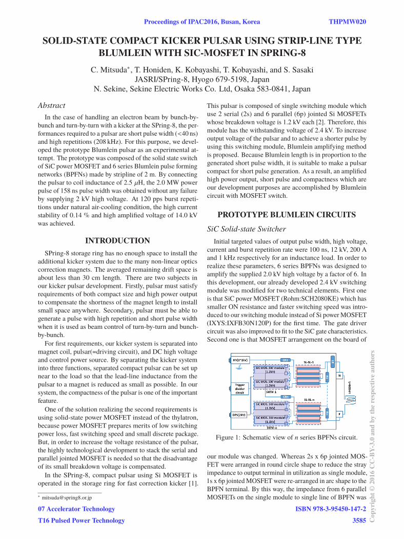
Figure 1: Schematic view of n series BPFNs circuit.
our module was changed. Whereas 2s x 6p jointed MOS-
FET were arranged in round circle shape to reduce the stray
impedance to output terminal in utilization as single module,
1s x 6p jointed MOSFET were re-arranged in arc shape to the
BPFN terminal. By this way, the impedance from 6 parallel
MOSFETs on the single module to single line of BPFN was
Proceedings of IPAC2016, Busan, Korea THPMW020
07 Accelerator Technology
T16 Pulsed Power Technology
ISBN 978-3-95450-147-2
3585 Cop
yrig
ht©
2016
CC
-BY-
3.0
and
byth
ere
spec
tive
auth
ors
reduced. Finally, one BPFN circuit jointed to two series 1.2
kV switching modules had 2.4 kV withstanding voltage.
Table 1: Design Parameter of Single Line for 3 and 6 BPFNs.
Parameter/single line 6 series 3 series
WCu (mm) 30 16
Wp (mm) 40 40
Line length (m) 2.0 4.0
L (nH) 25 94
C (nF) 5.8 6.2
Z (Ω) 2.0 3.9
Transmission vel. (m/s) 1.65×10⁸
Resonance freq. (MHz) 262.8
Pulse width for R=40Ω (ns) 24 48
Pulse width for L=600nH (ns) 130 189
Output current for R=40Ω (A) 317 159
Output current for L=600nH (A) 139 112
Figure 1 shows the schematic view of the pulsar. The
pulsar is connected to the high voltage and controller power
source and trigger generator out of the accelerator tunnel
with 30 m cable in ground floating. In the schematic view,
except for the inductance load, the pulsar totally consists of
twelve 1.2 kV switching modules (SW), six stripline (SL)
BPFNs and trigger and controller power source distributors.
The current charged in the 99 kΩ resistor (CR shown in
the figure) is released at the external trigger (DG645) tim-
ing. Another 1.5 kΩ resistor (R) is also used as impedance
matching resistance for BPFN capacity. The resistor (LR)
between output terminal and BPFNs is composed of par-
allel jointed RC snuber, 200 Ω limiting resistor and super
fast diode (IXYS, DSEP30-12CR) bank which suppress the
undershoot of the output pulse.
Stripline Type Blumlein
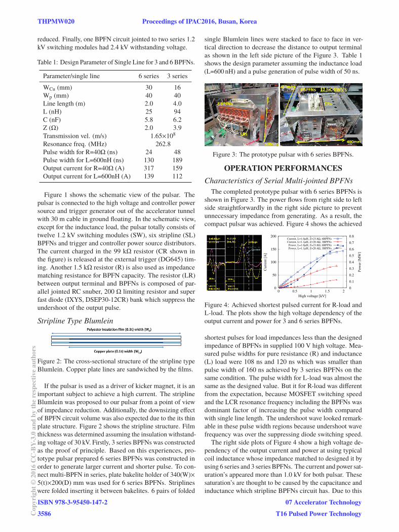
Figure 2: The cross-sectional structure of the stripline type
Blumlein. Copper plate lines are sandwiched by the films.
If the pulsar is used as a driver of kicker magnet, it is an
important subject to achieve a high current. The stripline
Blumlein was proposed to our pulsar from a point of view
of impedance reduction. Additionally, the downsizing effect
of BPFN circuit volume was also expected due to the its thin
plate structure. Figure 2 shows the stripline structure. Film
thickness was determined assuming the insulation withstand-
ing voltage of 30 kV. Firstly, 3 series BPFNs was constructed
as the proof of principle. Based on this experiences, pro-
totype pulsar prepared 6 series BPFNs was constructed in
order to generate larger current and shorter pulse. To con-
nect multi-BPFN in series, plate bakelite holder of 340(W)×5(t)×200(D) mm was used for 6 series BPFNs. Striplines
were folded inserting it between bakelites. 6 pairs of folded
single Blumlein lines were stacked to face to face in ver-
tical direction to decrease the distance to output terminal
as shown in the left side picture of the Figure 3. Table 1
shows the design parameter assuming the inductance load
(L=600 nH) and a pulse generation of pulse width of 50 ns.
Figure 3: The prototype pulsar with 6 series BPFNs.
OPERATION PERFORMANCESCharacteristics of Serial Multi-jointed BPFNs
The completed prototype pulsar with 6 series BPFNs is
shown in Figure 3. The power flows from right side to left
side straightforwardly in the right side picture to prevent
unnecessary impedance from generating. As a result, the
compact pulsar was achieved. Figure 4 shows the achieved
0
50
100
150
200
0 0.5 1 1.5 2 0
0.1
0.2
0.3
0.4
0.5
0.6
0.7
0.8
Cur
rent
[A]
Pow
er [M
W]
High voltage [kV]
Current, L=1.0μH, Z=23.8Ω, 6BPFNs
Current, L=1.1μH, Z=20.4Ω, 3BPFNs
Power, L=1.0μH, Z=23.8Ω, 6BPFNs
Power, L=1.1μH, Z=20.4Ω, 3BPFNs
Figure 4: Achieved shortest pulsed current for R-load and
L-load. The plots show the high voltage dependency of the
output current and power for 3 and 6 series BPFNs.
shortest pulses for load impedances less than the designed
impedance of BPFNs in supplied 100 V high voltage. Mea-
sured pulse widths for pure resistance (R) and inductance
(L) load were 108 ns and 120 ns which was smaller than
pulse width of 160 ns achieved by 3 series BPFNs on the
same condition. The pulse width for L-load was almost the
same as the designed value. But it for R-load was different
from the expectation, because MOSFET switching speed
and the LCR resonance frequency including the BPFNs was
dominant factor of increasing the pulse width compared
with single line length. The undershoot wave looked remark-
able in these pulse width regions because undershoot wave
frequency was over the suppressing diode switching speed.
The right side plots of Figure 4 show a high voltage de-
pendency of the output current and power at using typical
coil inductance whose impedance matched to designed it by
using 6 series and 3 series BPFNs. The current and power sat-
uration’s appeared more than 1.0 kV for both pulsar. These
saturation’s are thought to be caused by the capacitance and
inductance which stripline BPFNs circuit has. Due to this
THPMW020 Proceedings of IPAC2016, Busan, Korea
ISBN 978-3-95450-147-2
3586Cop
yrig
ht©
2016
CC
-BY-
3.0
and
byth
ere
spec
tive
auth
ors
07 Accelerator Technology
T16 Pulsed Power Technology

saturation, the measured current was almost the same as the
estimation for L-load (L=600 nH).
Figure 5 shows the impedance dependency of the output
power and gain efficiency (Eff.=Voutput/6or3×Vsupply×100.)
for the BPFNs series number at the 100 V high voltage supply.
The matching impedance was indicated at about 45 Ω for
L and R load. Although the BPFN designed impedance
of 24 Ω was not consistent with measured results due to
underestimating the blumlein capacitance, the impedance
of multi-stacking BPFNs circuit was kept low as expected
by using stripline BPFN. It was confirmed that the output
power for R-load was exactly increased by a factor of 2
by increasing series number of BPFN from 3 to 6. Then,
as noteworthy result, the high gain-efficiency of 80% was
obtained for L-load.
0
2
4
6
8
10
12
14
0 20 40 60 80 100 0
20
40
60
80
100
120
140
0 0.02 0.04 0.06 0.08 0.1 0.12 0.14 0.16
Pow
er [k
W]
Effic
ienc
y [%
]
Z [Ω]
Inductance [μH]
Power for R-load, 6BPFNs
Power for R-load, 3BPFNs
Efficeincy for R-load, 6BPFNs
Efficeincy for R-load, 3BPFNs
0
2
4
6
8
10
12
0 10 20 30 40 50 60 0
20
40
60
80
100
120 0 0.5 1 1.5 2 2.5 3
Pow
er [k
W]
Effic
ienc
y [%
]
Z [Ω]
Inductance [μH]
Power for L-load, 6BPFNs
Power for L-load, 3BPFNs
Efficeincy for L-load, 6BPFNs
Efficiency for L-load, 3BPFNs
Figure 5: The R and L load impedance dependency of the
output power and gain efficiency for the number of BPFNs.
Jitter of Multi-stacked SiC Switches
Table 2: Jitters for Pulse Width and Fire Timing
Burst repetition 1 pps 100 pps
Firing jitter (ps) at 100 V 186.6±10.6 180.5±7.9
Firing jitter (ps) at 1 kV 120.1±15.0 119.9±6.1
Pulse width jitter (ps) 86.5±4.6 89.4±2.2
Table 2 shows the timing jitter for firing and pulse width
at 300 V high voltage supply. In the measurement of firing
jitter, the jitter of about 30 ps which trigger generator has
was included. Although our pulsar must drives whole 72
switching elements simultaneously, the jitter level was kept
low enough to satisfy the requirement of beam operation.
There was a tendency that the jitter was slightly increased in
supplying high voltage of less than 300 V in this measure-
ment. It is thought to be caused due to the SiC solid state
characteristics. Figure 6 shows current stability for the burst
repetitions in the high power operation test. From 1 pps to 1
kpps, it was also kept <0.1%.
FIRST HIGH POWER OPERATION TEST
0.1
1
10
100
101
102
103
0.001
0.01
0.1
1
Pow
er [M
W]
Cur
rent
stab
ility
[%]
Burst repetition rate [pps]
Output power, 1kV supplied, L=1.0μH
Output current stability, L=1.0μH
Output power, 2kV supplied, L=2.5μH
Output current stability, L=2.5μH
Figure 6: The pulse shape at 120 pps high power test and the
plots show the power and current stability for repetitions.
First of all, the low power and 1 kpps burst repetition
test was tried under the condition which the pulsar was con-
nected 1.0 μH inductance coil and the 1.0 kV high voltage
was supplied. Maximum power was 0.27 MW.As shown in
Figure 6, the output power and current stability tended to
decrease in the burst repetition of more than 200 pps. At this
test, the surface temperature of charging resistor, switching
module, and blumlein circuit increased by 60, 2, and 7 ◦Cunder natural air-cooling condition. The resistances in the
circuit were changed by the heat generation whereas SiC
MOSFET had little heating loss for high repetitions. The
highest power output of 2.0 MW and amplified voltage of
14.0 kV was achieved for the inductance load (L=2.5 μH).
The measured output current is shown in Figure 6. On this
condition, the 120 pps burst repetition was succeeded under
natural air-cooling. The burst repetition rate was limited by
the temperature of the charging register in this test.
CONCLUSIONThe prototype pulsar must be improved for the tempera-
ture increasing of the resistor and blumlein circuit by using
fan or water cooling system for higher burst repetition test.
However, the combination of the stripline BPFN and SiC
solid-state switch showed the high capability in the point of
the stability, high burst repetition, and high power output for
L-load. And, it also demonstrated to achieve the downsizing
of the pulsar volume even for high power output.
REFERENCES[1] C. Mitsuda, et al., proc. of IPAC’14, Dresden, Ger-
many(2014),p280
[2] C. Mitsuda, et al., proc. of IPAC’13, Shanghai,
China(2013),p666
Proceedings of IPAC2016, Busan, Korea THPMW020
07 Accelerator Technology
T16 Pulsed Power Technology
ISBN 978-3-95450-147-2
3587 Cop
yrig
ht©
2016
CC
-BY-
3.0
and
byth
ere
spec
tive
auth
ors