SoC with the Satellite Navigation Unit based on the … · SoC with the Satellite Navigation Unit...
22
SoC with the Satellite Navigation Unit based on the single-core Rocket chip Khabarov Sergey, Nefedov Denis
Transcript of SoC with the Satellite Navigation Unit based on the … · SoC with the Satellite Navigation Unit...

SoC with the Satellite Navigation Unit based on the single-core
Rocket chipKhabarov Sergey,
Nefedov Denis

Who we are:• The startup company that emerged with the support of the “Laboratory of
Modeling and Design of Special Computer Systems Architectures” of Moscow Institute of Physics and Technology (MIPT)
Moscow Institute of Physics and Technology (S tate University), MIPT, 2015 2
Goal:
• To become a first prominent private ASIC design center in CIS region, that provides its customers their IP integration into SOC designs.
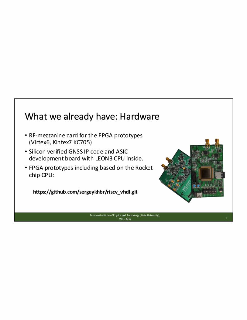
What we already have: Hardware
• RF-mezzanine card for the FPGA prototypes (Virtex6, Kintex7 KC705)• Silicon verified GNSS IP code and ASIC
development board with LEON3 CPU inside.• FPGA prototypes including based on the Rocket-
chip CPU:
https://github.com/sergeykhbr/riscv_vhdl.git
Moscow Institute of Physics and Technology (S tate University), MIPT, 2015 3

What we already have: Software
• Universal receiver firmware with the plug-n-play support for different targets: ASIC, FPGA and behavior simulation.• Host application for data analysis• See details:
www.gnss-sensor.com
Moscow Institute of Physics and Technology (S tate University), MIPT, 2015 4

ASIC design complexity:• Chip area: 10800x10800 um2
• 180nm CMOS process• 32 x Channels GNSS engine• 3 x Fast Search Engines (GPS/Glonass/Galileo)• 512KB Internal SRAM• 4KB (boot) + 128KB (FW) ROM• CPU with MMU and 16KB x2(I/D) Caches
Moscow Institute of Physics and Technology (S tate University), MIPT, 2015 5

What we are doing now:
Moscow Institute of Physics and Technology (S tate University), MIPT, 2015 6
ARCH: SPARC V8CPU: LEON3 32-bitsFPU: NoneTech: 180 nmFreq: 120 MHz
ARCH: RISC-VCPU: Rocket-chipFPU: YesTech: 90 nmFreq: 300 MHz
• Demonstration of portability of the Satellite Navigation IP.• Learn the new CPU architecture.
Rocket-chip based SoC goals:• Modular• Portable• Written in VHDL• Standard interfaces• CAD tool independence• Uniform method for HW & SW debug• Plug-n-play support• Transfer design on RISC-V architecture using all the best ideas of the GPL
licensed ‘grlib’ library.
Moscow Institute of Physics and Technology (S tate University), MIPT, 2015 7

Overview of the Rocket-chip based mockup
Available on: https://github.com/sergeykhbr/riscv_vhdl.gitMoscow Institute of Physics and Technology (S tate University),
MIPT, 2015 8
ROM: Boot0x00000000
ROM: FWImage0x00010000
RAM: 512 KB0x10000000
GPIO0x80000000
UART0x80001000
IRQController0x80002000
PNP config.0xFFFFF000
VHDL Bridge:
TileLinkIOAXI4 (NASTI)
RocketTile
cached
uncached
HostIO
AXI BUS interface
IRQ pins

Portability:• Process portability achieved through block wrappers.• Definition of 'virtual' components (PLL, IO pads, memory etc.).• Size, technology etc. are set through VHDL generics.• Technology specific mega-cells are instantiated with VHDL generate
statements.• Modular design - new technology easily added• Support of both ASIC and FPGA technologies • Example:
https://github.com/sergeykhbr/riscv_vhdl.git
Moscow Institute of Physics and Technology (S tate University), MIPT, 2015 9

CAD tools independence:• Robust coding style – 'least common denominator‘ inherited from GRLIB.• Project supports all major CAD tools.• Mentor, Cadence, Synopsys• ISE Studio, Vivado, Quartus.
• New CAD tool easily added but needs thorough testing.
Moscow Institute of Physics and Technology (S tate University), MIPT, 2015 10
Plug and Play
Moscow Institute of Physics and Technology (S tate University), MIPT, 2015 11
• Inherited from GRLIB method to quickly assemble a complex SOC design.• PCI-style plug&play support for AMBA (AXI4) configuration.• Device, ID, Vendor ID and version identification.• Address and interrupt configuration• Cacheability, pre-fetch information
• Several memory BARs per slave device.• Configuration set through VHDL generics• Plug&play information routed in sideband signals accessible via dedicated
slave device on system bus.• Fully compatible with AMBA AXI4.

UART output example
Moscow Institute of Physics and Technology (S tate University), MIPT, 2015 12
[uart0] # RISC-V: Rocket-Chip demonstration design[uart0] # HW version: 0x20151217[uart0] # Target technology: Virtex6[uart0] # AXI4: slv0: GNSS Sensor Ltd. Boot ROM[uart0] # 0x00000000...0x00001FFF, size = 8 KB[uart0] # AXI4: slv1: GNSS Sensor Ltd. FW Image ROM[uart0] # 0x00100000...0x0013FFFF, size = 256 KB[uart0] # AXI4: slv2: GNSS Sensor Ltd. Internal SRAM[uart0] # 0x10000000...0x1007FFFF, size = 512 KB[uart0] # AXI4: slv3: GNSS Sensor Ltd. Generic GPIO[uart0] # 0x80000000...0x80000FFF, size = 4 KB[uart0] # AXI4: slv4: GNSS Sensor Ltd. Generic UART[uart0] # 0x80001000...0x80001FFF, size = 4 KB[uart0] # AXI4: slv5: GNSS Sensor Ltd. Interrupt Controller[uart0] # 0x80002000...0x80002FFF, size = 4 KB[uart0] # AXI4: slv6: GNSS Sensor Ltd. GNSS Engine[uart0] # 0x80003000...0x80003FFF, size = 4 KB

Repository features
Moscow Institute of Physics and Technology (S tate University), MIPT, 2015 13
• Plug-n-play configuration module with the AXI interface.• Interrupt controller with the AXI interface either as UART and GPIO.• Project includes generic parameter allowing enable/disable L1toL2 interconnect
(L2 cache).• GNSS related functionality was stubbed• SoC implements self-loading procedure from the Boot ROM just after reset (see
next slide).• Constraints and ISE Studio projects files included.
This is ready-to-use SoC template for the Virtex6 and Kintex7 FPGA boards (ML605, KC705) that sequentially turns on/off LEDs and prints PnP information into UART.

Memory access optimization
Moscow Institute of Physics and Technology (S tate University), MIPT, 2015 14
• Single core.• L2 cache disabled• Read/Write access to the AXI peripheries for one clock cycle.
Burst read example1 clock address request + 4 clocks burst operation

Boot procedure overview
Moscow Institute of Physics and Technology (S tate University), MIPT, 2015 15
• Registers initialization.• Copying ROM FW Image into internal SRAM (total 512 KB available).• Go to SRAM entry point 0x10000000 in user mode.• Initialization of the “Interrupt Registers” by proper handler.• Initialization of the UART• Start main task.Features:• Automatic Detection of the target (Simulation, FPGA). • Speed-up behavior simulation by selecting reduced registers values.• One firmware for all platforms.
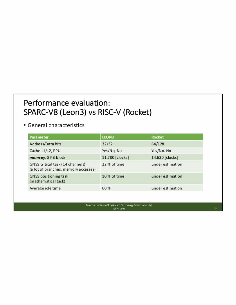
Performance evaluation: SPARC-V8 (Leon3) vs RISC-V (Rocket)
Moscow Institute of Physics and Technology (S tate University), MIPT, 2015 16
• General characteristics
Parameter LEON3 Rocket
Address/Data bits 32/32 64/128
Cache L1/L2, FPU Yes/No, No Yes/No, No
memcpy, 8 KB block 11.780 [clocks] 14.630 [clocks]
GNSS critical task (14 channels)(a lot of branches, memory accesses)
22 % of time under estimation
GNSS positioning task(mathematical task)
10 % of time under estimation
Average idle time 60 % under estimation

Our next step
Moscow Institute of Physics and Technology (S tate University), MIPT, 2015 17
• Producing SOC on 90 nm technology with the 256 channels GNSS engine.• Add L2/L3/L5 bandwidth support in GNSS Engine.
We have a lot of difficulties with the firmware debugging due to the lack of a convenient debugger and one general problem is:• Receiver’s firmware processing depends of the satellites constellation and
noise condition.
So, we’ve decided to implement our own Debug Support Unit (DSU) on the system bus using experience with a similar device in GRLIB and own software with OS Windows support.
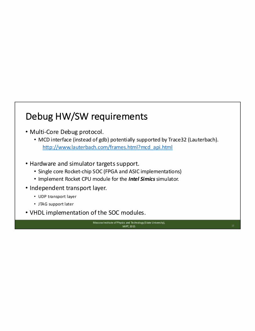
Debug HW/SW requirements
Moscow Institute of Physics and Technology (S tate University), MIPT, 2015 18
• Multi-Core Debug protocol.• MCD interface (instead of gdb) potentially supported by Trace32 (Lauterbach).
http://www.lauterbach.com/frames.html?mcd_api.html
• Hardware and simulator targets support.• Single core Rocket-chip SOC (FPGA and ASIC implementations)• Implement Rocket CPU module for the Intel Simics simulator.
• Independent transport layer.• UDP transport layer
• JTAG support later
• VHDL implementation of the SOC modules.

Real HW debug structure
Moscow Institute of Physics and Technology (S tate University), MIPT, 2015 19
Real Hardware
User's Front-end
1. Own application.
2. Compatible with the Trace32 by Lauterbach
HostLibrary
MACwithEDCL
TAP
AXI4Master
AXI B
US in
terfa
ce
DSU
CPU"Rocket"
HostIO
UDP
JTAG(postponed)
MCD
Debug description
Moscow Institute of Physics and Technology (S tate University), MIPT, 2015 20
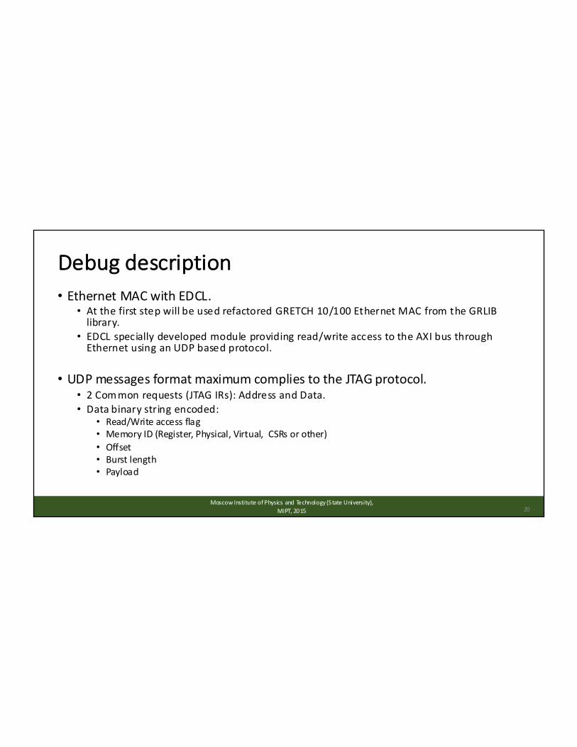
• Ethernet MAC with EDCL.• At the first step will be used refactored GRETCH 10/100 Ethernet MAC from the GRLIB
library.• EDCL specially developed module providing read/write access to the AXI bus through
Ethernet using an UDP based protocol.
• UDP messages format maximum complies to the JTAG protocol.• 2 Com mon requests (JTAG IRs): Address and Data.• Data binary string encoded:
• Read/Write access flag• Memory ID (Register, Physical, Virtual, CSRs or other)• Offset• Burst length• Payload

Ideal simulator in our opinion
Moscow Institute of Physics and Technology (S tate University), MIPT, 2015 21
We have enough experience to develop functional model of the RISC-V CPU using Simics API. It depends on the demands.Lauterbach has to become interested to support new architecture.
User's Front-end: Trace32
MCD
Simics with the loaded RISC-V platform

That’s all
Moscow Institute of Physics and Technology (S tate University), MIPT, 2015 22
• Thank you for your attention.
• GNSS related information:www.gnss-sensor.com
• Open source repository with the VHDL SOC template:https://github.com/sergeykhbr/riscv_vhdl.git