SN54ACT8990, SN74ACT8990 TEST-BUS CONTROLLERS …
20
SN54ACT8990, SN74ACT8990 TEST-BUS CONTROLLERS IEEE STD 1149.1 (JTAG) TAP MASTERS WITH 16-BIT GENERIC HOST INTERFACES SCAS190E – JUNE 1990 – REVISED JANUARY 1997 1 POST OFFICE BOX 655303 • DALLAS, TEXAS 75265 Members of the Texas Instruments SCOPE Family of Testability Products Compatible With the IEEE Standard 1149.1-1990 (JTAG) Test Access Port and Boundary-Scan Architecture Control Operation of Up to Six Parallel Target Scan Paths Accommodate Pipeline Delay to Target of Up to 31 Clock Cycles Scan Data Up to 2 32 Clock Cycles Execute Instructions for Up to 2 32 Clock Cycles Each Device Includes Four Bidirectional Event Pins for Additional Test Capability Inputs Are TTL-Voltage Compatible EPIC (Enhanced-Performance Implanted CMOS) 1-μm Process Packaged in 44-Pin Plastic Leaded Chip Carrier (FN), 68-Pin Ceramic Pin Grid Array (GB), and 68-Pin Ceramic Quad Flat Packages (HV) description The ’ACT8990 test-bus controllers (TBC) are members of the Texas Instruments SCOPE testability integrated-circuit family. This family of components supports IEEE Standard 1149.1-1990 (JTAG) boundary scan to facilitate testing of complex circuit-board assemblies. The ’ACT8990 differ from other SCOPE integrated circuits. Their function is to control the JTAG serial-test bus rather than being target boundary -scannable devices. The required signals of the JTAG serial-test bus – test clock (TCK), test mode select (TMS), test data input (TDI), and test data output (TDO) can be connected from the TBC to a target device without additional logic. This is done as a chain of IEEE Standard 1149.1-1990 boundary-scannable components that share the same serial-test bus. The TBC generates TMS and TDI signals for its target(s), receives TDO signals from its target(s), and buffers its test clock input (TCKI) to a test clock output (TCKO) for distribution to its target(s). The TMS, TDI, and TDO signals can be connected to a target directly or via a pipeline, with a retiming delay of up to 31 bits. Since the TBC can be configured to generate up to six separate TMS signals [TMS (5 – 0)], it can be used to control up to six target scan paths that are connected in parallel (i.e., sharing common TCK, TDI, and TDO signals). While most operations of the TBC are synchronous to TCKI, a test-off (TOFF ) input is provided for output control of the target interface, and a test-reset (TRST ) input is provided for hardware/software reset of the TBC. In addition, four event [EVENT (3 – 0)] I/Os are provided for asynchronous communication to target device(s). Each event has its own event generation/detection logic, and detected events can be counted by two 16-bit counters. The TBC operates under the control of a host microprocessor/microcontroller via the 5-bit address bus [ADRS (4–0)] and the 16-bit read/write data bus [DATA (15–0)]. Read (RD ) and write (WR ) strobes are implemented such that the critical host-interface timing is independent of the TCKI period. Any one of 24 registers can be addressed for read and/or write operations. In addition to control and status registers, the TBC contains two command registers, a read buffer, and a write buffer. Status of the TBC is transmitted to the host via ready (RDY ) and interrupt (INT ) outputs. Major commands can be issued by the host to cause the TBC to generate the TMS sequences necessary to move the target(s) from any stable test-access-port (TAP) controller state to any other stable TAP state, to execute instructions in the Run-Test/Idle TAP state, or to scan instruction or test data through the target(s). A 32-bit counter can be preset to allow a predetermined number of execution or scan operations. Serial data that appears at the selected TDI input (TDI1 or TDI0) is transferred into the read buffer, which can be read by the host to obtain up to 16 bits of the serial-data stream. Serial data that is transmitted from the TDO output is written by the host to the write buffer. Copyright 1997, Texas Instruments Incorporated PRODUCTION DATA information is current as of publication date. Products conform to specifications per the terms of Texas Instruments standard warranty. Production processing does not necessarily include testing of all parameters. SCOPE and EPIC are trademarks of Texas Instruments Incorporated. Please be aware that an important notice concerning availability, standard warranty, and use in critical applications of Texas Instruments semiconductor products and disclaimers thereto appears at the end of this data sheet. On products compliant to MIL-PRF-38535, all parameters are tested unless otherwise noted. On all other products, production processing does not necessarily include testing of all parameters.
Transcript of SN54ACT8990, SN74ACT8990 TEST-BUS CONTROLLERS …

SN54ACT8990, SN74ACT8990TEST-BUS CONTROLLERS
IEEE STD 1149.1 (JTAG) TAP MASTERS WITH 16-BIT GENERIC HOST INTERFACES
SCAS190E – JUNE 1990 – REVISED JANUARY 1997
1POST OFFICE BOX 655303 • DALLAS, TEXAS 75265
Members of the Texas InstrumentsSCOPE Family of Testability Products
Compatible With the IEEE Standard1149.1-1990 (JTAG) Test Access Port andBoundary-Scan Architecture
Control Operation of Up to Six ParallelTarget Scan Paths
Accommodate Pipeline Delay to Target ofUp to 31 Clock Cycles
Scan Data Up to 2 32 Clock Cycles
Execute Instructions for Up to 2 32 ClockCycles
Each Device Includes Four BidirectionalEvent Pins for Additional Test Capability
Inputs Are TTL-Voltage Compatible
EPIC (Enhanced-Performance ImplantedCMOS) 1-µm Process
Packaged in 44-Pin Plastic Leaded ChipCarrier (FN), 68-Pin Ceramic Pin Grid Array(GB), and 68-Pin Ceramic Quad FlatPackages (HV)
description
The ’ACT8990 test-bus controllers (TBC) are members of the Texas Instruments SCOPE testabilityintegrated-circuit family. This family of components supports IEEE Standard 1149.1-1990 (JTAG) boundaryscan to facilitate testing of complex circuit-board assemblies. The ’ACT8990 differ from other SCOPEintegrated circuits. Their function is to control the JTAG serial-test bus rather than being targetboundary-scannable devices.
The required signals of the JTAG serial-test bus – test clock (TCK), test mode select (TMS), test data input (TDI),and test data output (TDO) can be connected from the TBC to a target device without additional logic. This isdone as a chain of IEEE Standard 1149.1-1990 boundary-scannable components that share the sameserial-test bus. The TBC generates TMS and TDI signals for its target(s), receives TDO signals from its target(s),and buffers its test clock input (TCKI) to a test clock output (TCKO) for distribution to its target(s). The TMS, TDI,and TDO signals can be connected to a target directly or via a pipeline, with a retiming delay of up to 31 bits.Since the TBC can be configured to generate up to six separate TMS signals [TMS (5 –0)], it can be used tocontrol up to six target scan paths that are connected in parallel (i.e., sharing common TCK, TDI, and TDOsignals).
While most operations of the TBC are synchronous to TCKI, a test-off (TOFF) input is provided for output controlof the target interface, and a test-reset (TRST) input is provided for hardware/software reset of the TBC. Inaddition, four event [EVENT (3–0)] I/Os are provided for asynchronous communication to target device(s).Each event has its own event generation/detection logic, and detected events can be counted by two 16-bitcounters.
The TBC operates under the control of a host microprocessor/microcontroller via the 5-bit address bus[ADRS (4–0)] and the 16-bit read/write data bus [DATA (15–0)]. Read (RD) and write (WR) strobes areimplemented such that the critical host-interface timing is independent of the TCKI period. Any one of24 registers can be addressed for read and/or write operations. In addition to control and status registers, theTBC contains two command registers, a read buffer, and a write buffer. Status of the TBC is transmitted to thehost via ready (RDY) and interrupt (INT) outputs.
Major commands can be issued by the host to cause the TBC to generate the TMS sequences necessary tomove the target(s) from any stable test-access-port (TAP) controller state to any other stable TAP state, toexecute instructions in the Run-Test/Idle TAP state, or to scan instruction or test data through the target(s). A32-bit counter can be preset to allow a predetermined number of execution or scan operations.
Serial data that appears at the selected TDI input (TDI1 or TDI0) is transferred into the read buffer, which canbe read by the host to obtain up to 16 bits of the serial-data stream. Serial data that is transmitted from the TDOoutput is written by the host to the write buffer.
Copyright 1997, Texas Instruments IncorporatedPRODUCTION DATA information is current as of publication date.Products conform to specifications per the terms of Texas Instrumentsstandard warranty. Production processing does not necessarily includetesting of all parameters.
SCOPE and EPIC are trademarks of Texas Instruments Incorporated.
Please be aware that an important notice concerning availability, standard warranty, and use in critical applications ofTexas Instruments semiconductor products and disclaimers thereto appears at the end of this data sheet.
On products compliant to MIL-PRF-38535, all parameters are testedunless otherwise noted. On all other products, productionprocessing does not necessarily include testing of all parameters.

SN54ACT8990, SN74ACT8990TEST-BUS CONTROLLERSIEEE STD 1149.1 (JTAG) TAP MASTERS WITH 16-BIT GENERIC HOST INTERFACES
SCAS190E – JUNE 1990 – REVISED JANUARY 1997
2 POST OFFICE BOX 655303 • DALLAS, TEXAS 75265
description (continued)
The SN54ACT8990 is characterized for operation over the full military temperature range of –55°C to 125°C.The SN74ACT8990 is characterized for operation from 0°C to 70°C.
AD
RS
0G
ND
INT
NC
NC
AD
RS
4A
DR
S3
NC
AD
RS
2A
DR
S1
NC
DA
TA14 NC
DA
TA15
TO
FF
DA
TA10 NC
DA
TA11
DA
TA12 NC
DA
TA13NC
DA
TA9
RD
YR
DN
CT
DI0
TD
I1N
C
NC
WR
TR
ST
NC
28 29
NCTMS5/EVENT3TMS4/EVENT2NCTMS3/EVENT1TMS2/EVENT0NCVCCGNDTMS1NCTMS0TDONCTCKOTCKINC
60
59
58
57
56
55
54
53
52
51
50
49
48
47
46
45
4430
10
11
12
13
14
15
16
17
18
19
20
21
22
23
24
25
26
NCDATA0DATA1
NCDATA2DATA3
NCDATA4
GNDVCCNC
DATA5DATA6
NCDATA7DATA8
NC31 32 33 34
8 7 6 5 49 3 1 68 672
35 36 37 38 39
66 65
27
64 63 62 61
40 41 42 43
SN54ACT8990 . . . HV PACKAGE(TOP VIEW)
CC
V
NC – No internal connection
SN54ACT8990, SN74ACT8990TEST-BUS CONTROLLERS
IEEE STD 1149.1 (JTAG) TAP MASTERS WITH 16-BIT GENERIC HOST INTERFACES
SCAS190E – JUNE 1990 – REVISED JANUARY 1997
3POST OFFICE BOX 655303 • DALLAS, TEXAS 75265
RD
YR
DW
RT
RS
T
AD
RS
4A
DR
S3
AD
RS
2A
DR
S1
AD
RS
0G
ND
INT
DA
TA15
TO
FF
TD
I0T
DI1
DA
TA9
DA
TA10
DA
TA11
DA
TA12
DA
TA13
DA
TA14CC
V
SN74ACT8990 . . . FN PACKAGE(TOP VIEW)
TMS5/EVENT3TMS4/EVENT2TMS3/EVENT1TMS2/EVENT0VCCGNDTMS1TMS0TDOTCKOTCKI
39
38
37
36
35
34
33
32
31
30
2918 19
7
8
9
10
11
12
13
14
15
16
17
DATA0DATA1DATA2DATA3DATA4
GNDVCC
DATA5DATA6DATA7DATA8
20 21 22 23
5 4 3 2 16 44
42 41 4043
24 25 26 27 28
K
1 2 3 4 5 6 7 8 9 10 11
J
H
G
F
E
D
C
B
A
L
SN54ACT8990 . . . GB PACKAGE(TOP VIEW)

SN54ACT8990, SN74ACT8990TEST-BUS CONTROLLERSIEEE STD 1149.1 (JTAG) TAP MASTERS WITH 16-BIT GENERIC HOST INTERFACES
SCAS190E – JUNE 1990 – REVISED JANUARY 1997
4 POST OFFICE BOX 655303 • DALLAS, TEXAS 75265
Table 1. Terminal Assignments
TERMINAL TERMINAL TERMINAL TERMINAL
NO. NAME NO. NAME NO. NAME NO. NAME
A2 NC B10 NC F11 NC K6 NC
A3 ADRS4 B11 NC G1 DATA5 K7 VCC
A4 NC C1 DATA2 G2 NC K8 DATA15
A5 ADRS1 C2 DATA1 G10 NC K9 TDI0
A6 ADRS0 C3 NC G11 TMS1 K10 NC
A7 NC C10 TMS4/EVENT2 H1 NC K11 TCKI
A8 INT C11 TMS5/EVENT3 H2 DATA6 L2 DATA9
A9 RD D1 DATA4 H10 TDO L3 NC
A10 TRST D2 DATA3 H11 TMS0 L4 DATA12
B1 DATA0 D10 TMS3/EVENT1 J1 DATA8 L5 DATA13
B2 NC D11 NC J2 DATA7 L6 NC
B3 ADRS3 E1 NC J10 TCKO L7 DATA14
B4 ADRS2 E2 GND J11 NC L8 TOFF
B5 NC E10 VCC K1 NC L9 TDI1
B6 NC E11 TMS2/EVENT0 K2 NC L10 NC
B7 GND F1 VCC K3 DATA10
B8 RDY F2 NC K4 DATA11
B9 WR F10 GND K5 NC
NC – No internal connection
functional block diagram
4
2
2
16
1616
5
RD
WR
RDY
INT
ADRS(4–0)
DATA(15–0)†
HostInterface
TargetInterface
TMS(5–2)/EVENT(3–0)†
TMS(1–0)
TDI(1–0)†
TDO
TOFF†
TCKO
TCKI
TRST†
EventBlock
SequencerBlock
Counter Block
Command Block
Serial Block
HostBlock
Read Data Bus
Write Data Bus
† Inputs have internal pullup resistors.

SN54ACT8990, SN74ACT8990TEST-BUS CONTROLLERS
IEEE STD 1149.1 (JTAG) TAP MASTERS WITH 16-BIT GENERIC HOST INTERFACES
SCAS190E – JUNE 1990 – REVISED JANUARY 1997
5POST OFFICE BOX 655303 • DALLAS, TEXAS 75265
Terminal Functions
TERMINAL NAME I/O DESCRIPTION
ADRS4– ADRS0 IAddress inputs. ADRS4– ADRS0 form the 5-bit address bus that interfaces the TBC to its host. These inputsspecify the TBC register to be read from or written to.
DATA15–DATA0 I/OData inputs and outputs. DATA15–DATA0 form the 16-bit bidirectional data bus that interfaces the TBC to itshost. Data is read from or written to the TBC register using this data bus.
GND Ground
INT OInterrupt. INT transmits an interrupt signal to the host. When the TBC requires service from the host, INT isasserted (low). INT will remain asserted (low) until the host has completed the required service.
NC No connection
RD IRead strobe. RD is the active low output enable for the data bus. RD is used as the strobe for reading data fromthe selected TBC register.
RDY OReady. RDY transmits a status signal to the host. When the TBC is ready to accept a read or write operationfrom the host, RDY is asserted (low). RDY is not asserted (high) when the TBC is in recovery from a read, write,command, or reset operation.
TCKI ITest clock input. TCKI is the clock input for the TBC. Most operations of the TBC are synchronous to TCKI.When enabled, all target interface outputs change on the falling edge of TCKI. Sampling of target interfaceinputs are configured to occur on either the rising edge or falling edge of TCKI.
TCKO OTest clock output. TCKO distributes TCK to the target(s). The TCKO is configured to be disabled, constant zero,constant one, or to follow TCKI. When TCKO follows TCKI, it is delayed to match the delay of generating theTDO and TMS signals.
TDI1–TDI0 ITest data inputs. The TDI1–TDI0 serial inputs are used for shifting test data from the target(s). The TDI inputscan be directly connected to the TDO pin(s) of the target(s).
TDO OTest data output. TDO is used for shifting test data into the target(s). TDO can be directly connected to the TDIterminal(s) of the target(s).
TMS1–TMS0 OTest mode select outputs. These parallel outputs transmit TMS signals to the target(s), which direct themthrough their TAP controller states. TMS1–TMS0 can be directly connected to the TMS terminals of thetarget(s).
TMS5–TMS2/EVENT3–EVENT0
I/OTest mode select outputs or event inputs/outputs. These I/Os can be configured for use as either TMS outputsor event inputs/outputs. As TMS outputs, they function similarly to TMS1–TMS0 above. As event I/Os, theycan be used to receive/transmit interrupt signals to/from the target(s).
TOFF ITest-off input. TOFF is the active low output disable for all outputs and I/Os of the target interface (TCKO, TDO,TMS, TMS/EVENT).
TRST ITest-reset input. TRST is used to initiate hardware and software reset operations of the TBC. Hardware resetbegins when TRST is asserted (low). Software reset begins when TRST is released (high) and proceedssynchronously to TCKI to completion in a predetermined number of cycles.
WR IWrite input. WR is the strobe for writing data to a TBC data register. Signals present at the data and addressbuses are captured on the rising edge of WR.
VCC Supply voltage

SN54ACT8990, SN74ACT8990TEST-BUS CONTROLLERSIEEE STD 1149.1 (JTAG) TAP MASTERS WITH 16-BIT GENERIC HOST INTERFACES
SCAS190E – JUNE 1990 – REVISED JANUARY 1997
6 POST OFFICE BOX 655303 • DALLAS, TEXAS 75265
absolute maximum ratings over operating free-air temperature range (unless otherwise noted) †
Supply voltage range, VCC –0.5 V to 7 V. . . . . . . . . . . . . . . . . . . . . . . . . . . . . . . . . . . . . . . . . . . . . . . . . . . . . . . . . . Input voltage range, VI (see Note 1) –0.5 V to VCC. . . . . . . . . . . . . . . . . . . . . . . . . . . . . . . . . . . . . . . . . . . . . . . . . Output voltage range, VO (see Note 1) –0.5 V to VCC. . . . . . . . . . . . . . . . . . . . . . . . . . . . . . . . . . . . . . . . . . . . . . Input clamp current, IIK (VI < 0 or VI > VCC) ±20 mA. . . . . . . . . . . . . . . . . . . . . . . . . . . . . . . . . . . . . . . . . . . . . . . . Output clamp current, IOK (VO < 0 or VO > VCC) ±20 mA. . . . . . . . . . . . . . . . . . . . . . . . . . . . . . . . . . . . . . . . . . . . Continuous output current, IO (VO = 0 to VCC) ±25 mA. . . . . . . . . . . . . . . . . . . . . . . . . . . . . . . . . . . . . . . . . . . . . . Maximum power dissipation at TA = 55°C (in still air) (see Note 2): FN package 1.5W. . . . . . . . . . . . . . . . . . . Storage temperature range, Tstg –65°C to 150°C. . . . . . . . . . . . . . . . . . . . . . . . . . . . . . . . . . . . . . . . . . . . . . . . . . .
† Stresses beyond those listed under “absolute maximum ratings” may cause permanent damage to the device. These are stress ratings only, andfunctional operation of the device at these or any other conditions beyond those indicated under “recommended operating conditions” is notimplied. Exposure to absolute-maximum-rated conditions for extended periods may affect device reliability.
NOTES: 1. The input and output voltage ratings may be exceeded if the input and output clamp-current ratings are observed.2. The maximum package power dissipation is calculated using a junction temperature of 150°C and a board trace length of 75 mils.
For more information, refer to the Package Thermal Considerations application note in the ABT Advanced BiCMOS Technology DataBook, literature number SCBD002.
recommended operating conditions
SN54ACT8990 SN74ACT8990UNIT
MIN MAX MIN MAXUNIT
VCC Supply voltage 4.5 5.5 4.5 5.5 V
VIH High-level input voltage 2 2 V
VIL Low-level input voltage 0.8 0.8 V
VI Input voltage 0 VCC 0 VCC V
VO Output voltage 0 VCC 0 VCC V
IOH High-level output current –8 –8 mA
IOL Low-level output current 8 8 mA
TA Operating free-air temperature –55 125 0 70 °C

SN54ACT8990, SN74ACT8990TEST-BUS CONTROLLERS
IEEE STD 1149.1 (JTAG) TAP MASTERS WITH 16-BIT GENERIC HOST INTERFACES
SCAS190E – JUNE 1990 – REVISED JANUARY 1997
7POST OFFICE BOX 655303 • DALLAS, TEXAS 75265
electrical characteristics over recommended operating free-air temperature range (unlessotherwise noted)
PARAMETER TEST CONDITIONSTA = 25°C SN54ACT8990 SN74ACT8990
UNITPARAMETER TEST CONDITIONSMIN TYP† MAX MIN MAX MIN MAX
UNIT
VCC = 4 5 VIOH = –20 µA 4.4 4.4 4.4
VOH
VCC = 4.5 VIOH = –8 mA 3.7 3.7 3.7
VVOHVCC = 5 5 V
IOH = –20 µA 5.4 5.4 5.4V
VCC = 5.5 VIOH = –8 mA 4.7 4.7 4.7
VOLVCC = 4.5 V IOL = 20 µA 0.1 0.1 0.1
VVOLCC
to 5.5 V IOL = 8 mA 0.5 0.5 0.5V
I
ADRS, RD,WR, TCKI
VCC = 5.5 V, VI = VCC or GND ±1 ±1 ±1
AIITDI, TOFF, VCC = 5 5 V
VI = VCC ±1 ±1 ±1µA
TDI, TOFF,TRST
VCC = 5.5 VVI = GND –35 –70 –250 –35 –250 –35 –250
I ‡
INT, RDY, TCKO,TDO, TMS
VCC = 5.5 V, VO = VCC or GND ±10 ±10 ±10
AIOZ‡DATA,
VCC = 5 5 VVO = VCC ±10 ±10 ±10
µA,
TMS/EVENTVCC = 5.5 V
VO = GND –35 –70 –250 –35 –250 –35 –250
VCC = 5.5 V,VI = VCC or GND 450* 450 450 µA
IIO = 0,
VI = VCC or GND 450* 450 450 µA
ICC VCC = 5.5 V, CL = 50 pF100 mA
fclock = 30 MHz100 mA
Ci VI = VCC or GND 5* pF
Cio VI = VCC or GND 9* pF
Co VI = VCC or GND 8* pF
* On products compliant to MIL-PRF-38535, this parameter does not apply.† Typical values are at VCC = 5 V.‡ For I/O ports, the parameter IOZ includes the input leakage.

SN54ACT8990, SN74ACT8990TEST-BUS CONTROLLERSIEEE STD 1149.1 (JTAG) TAP MASTERS WITH 16-BIT GENERIC HOST INTERFACES
SCAS190E – JUNE 1990 – REVISED JANUARY 1997
8 POST OFFICE BOX 655303 • DALLAS, TEXAS 75265
timing requirements over recommended ranges of supply voltage and operating free-airtemperature (see Figure 1)
SN54ACT8990 SN74ACT8990UNIT
MIN MAX MIN MAXUNIT
fclock Clock frequency 0 30 0 30 MHz
RD low† 5.5 ns
WR low 5.5 5.5
tw Pulse duration EVENT high or low 8 8ns
TCKI high or low 10.5 10.5ns
TRST low 6 6
ADRS† before RD↑ 6.5 ns
ADRS before WR↑ 6.5 6.5
DATA before WR↑ 6 6
tsu Setup time EVENT before TCKI↑ 6 5.5ns
EVENT before TCKI↓ 5 5ns
TDI before TCKI↑ 2 2
TDI before TCKI↓ 2 2
ADRS† after RD↑ 5 ns
ADRS after WR↑ 5.5 5
DATA after WR↑ 5.5 5.5
th Hold time EVENT after TCKI↑ 5.5 5ns
EVENT after TCKI↓ 5 5ns
TDI after TCKI↑ 4 2.5
TDI after TCKI↓ 4 2.5† Applies only in the case where ADRS (4-0) = 10110 (read buffer).
SN54ACT8990, SN74ACT8990TEST-BUS CONTROLLERS
IEEE STD 1149.1 (JTAG) TAP MASTERS WITH 16-BIT GENERIC HOST INTERFACES
SCAS190E – JUNE 1990 – REVISED JANUARY 1997
9POST OFFICE BOX 655303 • DALLAS, TEXAS 75265
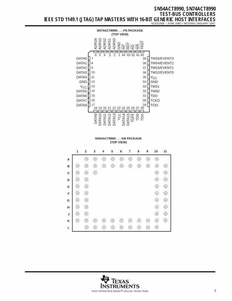
switching characteristics over recommended ranges of supply voltage and operating free-airtemperature (see Figure 1)
PARAMETERFROM TO SN54ACT8990 SN74ACT8990
UNITPARAMETER(INPUT) (OUTPUT) MIN MAX MIN MAX
UNIT
fmax 30 30 MHz
tPLHADRS DATA
8 43 19.5 39.3ns
tPHLADRS DATA
8 43 19.5 39.3ns
tPLHRD↑
RDY5.3 17 5.3 13.8
nstPLHWR↑
RDY2.5 16 2.5 13
ns
tPLHTCKI↑ INT
3.7 16 3.7 12.9ns
tPHLTCKI↑ INT
5.5 15 5.5 13.1ns
tPHL TCKI↑ RDY 4.4 15 4.4 13.4 ns
tPLH TCKI↑ TCKO 3.3 17 3.3 14.1 ns
tPLHTCKI↓ TCKO
2.3 19 2.3 15.9ns
tPHLTCKI↓ TCKO
3.6 17 3.6 15.6ns
tPLHTCKI↓ TDO
2.9 19 2.9 17.5ns
tPHLTCKI↓ TDO
5.2 20 5.2 17.9ns
tPLHTCKI↓ TMS
3.1 19 3.1 17.5ns
tPHLTCKI↓ TMS
5.1 19 5.1 18.2ns
tPLHTCKI↓ TMS/EVENT
1.5 19 1.5 17.5ns
tPHLTCKI↓ TMS/EVENT
3.5 20 3.5 18.9ns
tPZHRD↓ DATA
3.8 21 3.8 17.6ns
tPZLRD↓ DATA
6.8 28 6.8 22.6ns
tPZH TCKI↑INT 4.9 19 4.9 15.3
nstPZH TCKI↑RDY 3.6 19 3.6 15.3
ns
tPZHTCKI↓ TCKO
4.1 23 4.1 19.2ns
tPZLTCKI↓ TCKO
4.8 20 4.8 17.4ns
tPZHTCKI↓ TDO
4.3 22 4.3 19.5ns
tPZLTCKI↓ TDO
5 20 5 17.7ns
tPZHTCKI↓ TMS
4.6 23 4.6 19.9ns
tPZLTCKI↓ TMS
5.1 20 5.1 18.5ns
tPZHTCKI↓ TMS/EVENT
2 21 2 18.8ns
tPZLTCKI↓ TMS/EVENT
3.2 20 3.2 18.7ns
tPZHTOFF↑ TCKO
4.6 16 4.6 12.2ns
tPZLTOFF↑ TCKO
3.1 14 3.1 10.3ns
tPZHTOFF↑ TDO
4.4 15 4.4 12.2ns
tPZLTOFF↑ TDO
3.5 14 3.5 10.8ns
tPZHTOFF↑ TMS
3.1 16.2 3.1 14.7ns
tPZLTOFF↑ TMS
1.9 16.7 1.9 13.6ns

SN54ACT8990, SN74ACT8990TEST-BUS CONTROLLERSIEEE STD 1149.1 (JTAG) TAP MASTERS WITH 16-BIT GENERIC HOST INTERFACES
SCAS190E – JUNE 1990 – REVISED JANUARY 1997
10 POST OFFICE BOX 655303 • DALLAS, TEXAS 75265
switching characteristics over recommended ranges of supply voltage and operating free-airtemperature (continued) (see Figure 1)
PARAMETERFROM TO SN54ACT8990 SN74ACT8990
UNITPARAMETER(INPUT) (OUTPUT) MIN MAX MIN MAX
UNIT
tPZHTOFF↑ TMS/EVENT
2.3 15.3 2.3 13.8ns
tPZLTOFF↑ TMS/EVENT
2.7 16.4 2.7 13.9ns
tPHZRD↑ DATA
3.8 18.4 3.8 15.4ns
tPLZRD↑ DATA
4.1 17.1 4.1 14.8ns
tPHZTCKI↓ TCKO
6.7 20.4 6.7 19.8ns
tPLZTCKI↓ TCKO
4.8 21.1 4.8 20.4ns
tPHZTCKI↓ TDO
5.1 21.7 5.1 21.3ns
tPLZTCKI↓ TDO
5 20.7 5 20.3ns
tPHZTCKI↓ TMS
6.9 22.4 6.9 21.9ns
tPLZTCKI↓ TMS
4.6 20.6 4.6 20.1ns
tPHZTCKI↓ TMS/EVENT
4.7 22.5 4.7 22.1ns
tPLZTCKI↓ TMS/EVENT
2.8 20.5 2.8 20.1ns
tPHZTOFF↓ TCKO
5 15.6 5 15.4ns
tPLZTOFF↓ TCKO
4.4 15.5 4.4 15.3ns
tPHZTOFF↓ TDO
5.6 16.6 5.6 16.5ns
tPLZTOFF↓ TDO
4.6 15.4 4.6 15.4ns
tPHZTOFF↓ TMS
4.8 19.1 4.8 17.1ns
tPLZTOFF↓ TMS
4.4 17 4.4 15.8ns
tPHZTOFF↓ TMS/EVENT
4.5 18.8 4.5 17.3ns
tPLZTOFF↓ TMS/EVENT
2.4 17.1 2.4 16.2ns
tPHZTRST↓ DATA
5.7 23 5.7 20.8ns
tPLZTRST↓ DATA
4.2 20.3 4.2 20ns
tPHZTRST↓ INT
6 19.6 8 19.5ns
tPLZTRST↓ INT
6.1 18 6.1 17.8ns
tPHZTRST↓ RDY
6.5 18.8 6.5 18.7ns
tPLZTRST↓ RDY
4.8 17.8 4.8 17.8ns
tPHZTRST↓ TMS/EVENT
6 21.1 6 21.1ns
tPLZTRST↓ TMS/EVENT
4.2 20 4.2 19.9ns

SN54ACT8990, SN74ACT8990TEST-BUS CONTROLLERS
IEEE STD 1149.1 (JTAG) TAP MASTERS WITH 16-BIT GENERIC HOST INTERFACES
SCAS190E – JUNE 1990 – REVISED JANUARY 1997
11POST OFFICE BOX 655303 • DALLAS, TEXAS 75265
PARAMETER MEASUREMENT INFORMATION
thtsu
From Output Under Test
CL = 50 pF
LOAD CIRCUIT
S1
VCC
Open
GND
1 kΩ tPLH/tPHLtPLZ/tPZLtPHZ/tPZH
OpenVCCGND
OutputControl
(high-levelenabling)
OutputWaveform 1
S1 at VCC(see Note B)
OutputWaveform 2
S1 at GND(see Note B)
VOL
VOH
tPZL
tPZH
tPLZ
tPHZ
1.5 V1.5 V
≈ VCC
0 V
50% VCC≈ 0 V
3 VData Input
Timing Input 1.5 V
3 V
0 V
1.5 V 1.5 V3 V
0 V
3 V
0 V
1.5 V 1.5 V
tw
Input
(see Note A)
50% VCC 10% VCC
90% VCC
tPLHtPHL
1.5 V 1.5 V
3 V
0 V
50% VCC 50% VCC
VOH
VOL
Input
Output
VOLTAGE WAVEFORMSPULSE DURATION
VOLTAGE WAVEFORMSENABLE AND DISABLE TIMES
VOLTAGE WAVEFORMSPROPAGATION DELAY TIMES
VOLTAGE WAVEFORMSSETUP AND HOLD TIMES
TEST S1
NOTES: A. CL includes probe and jig capacitance.B. Waveform 1 is for an output with internal conditions such that the output is low except when disabled by the output control.
Waveform 2 is for an output with internal conditions such that the output is high except when disabled by the output control.C. All input pulses are supplied by generators having the following characteristics: PRR ≤ 10 MHz, ZO = 50 Ω, tr ≤ 3 ns, tf ≤ 3 ns.
For testing pulse duration: tr = tf = 1 to 3 ns. Pulse polarity can be either high-to-low-to-high or low-to-high-to-low.D. The outputs are measured one at a time with one transition per measurement.
Figure 1. Load Circuit and Voltage Waveforms

PACKAGE OPTION ADDENDUM
www.ti.com 9-Mar-2021
Addendum-Page 1
PACKAGING INFORMATION
Orderable Device Status(1)
Package Type PackageDrawing
Pins PackageQty
Eco Plan(2)
Lead finish/Ball material
(6)
MSL Peak Temp(3)
Op Temp (°C) Device Marking(4/5)
Samples
5962-9322801MXA ACTIVE CFP HV 68 1 Non-RoHS &Non-Green
Call TI N / A for Pkg Type -55 to 125 5962-9322801MXASNJ54ACT8990HV
5962-9322801MYA ACTIVE CPGA GB 68 1 Non-RoHS &Non-Green
SNPB N / A for Pkg Type -55 to 125 5962-9322801MYASNJ54ACT8990GB
SN74ACT8990FN ACTIVE PLCC FN 44 26 RoHS & Green NIPDAU Level-3-260C-168 HR -40 to 85 ACT8990
SN74ACT8990FNR ACTIVE PLCC FN 44 500 RoHS & Green NIPDAU Level-3-260C-168 HR -40 to 85 ACT8990
SNJ54ACT8990GB ACTIVE CPGA GB 68 1 Non-RoHS &Non-Green
SNPB N / A for Pkg Type -55 to 125 5962-9322801MYASNJ54ACT8990GB
SNJ54ACT8990HV ACTIVE CFP HV 68 1 Non-RoHS &Non-Green
Call TI N / A for Pkg Type -55 to 125 5962-9322801MXASNJ54ACT8990HV
(1) The marketing status values are defined as follows:ACTIVE: Product device recommended for new designs.LIFEBUY: TI has announced that the device will be discontinued, and a lifetime-buy period is in effect.NRND: Not recommended for new designs. Device is in production to support existing customers, but TI does not recommend using this part in a new design.PREVIEW: Device has been announced but is not in production. Samples may or may not be available.OBSOLETE: TI has discontinued the production of the device.
(2) RoHS: TI defines "RoHS" to mean semiconductor products that are compliant with the current EU RoHS requirements for all 10 RoHS substances, including the requirement that RoHS substancedo not exceed 0.1% by weight in homogeneous materials. Where designed to be soldered at high temperatures, "RoHS" products are suitable for use in specified lead-free processes. TI mayreference these types of products as "Pb-Free".RoHS Exempt: TI defines "RoHS Exempt" to mean products that contain lead but are compliant with EU RoHS pursuant to a specific EU RoHS exemption.Green: TI defines "Green" to mean the content of Chlorine (Cl) and Bromine (Br) based flame retardants meet JS709B low halogen requirements of <=1000ppm threshold. Antimony trioxide basedflame retardants must also meet the <=1000ppm threshold requirement.
(3) MSL, Peak Temp. - The Moisture Sensitivity Level rating according to the JEDEC industry standard classifications, and peak solder temperature.
(4) There may be additional marking, which relates to the logo, the lot trace code information, or the environmental category on the device.
PACKAGE OPTION ADDENDUM
www.ti.com 9-Mar-2021
Addendum-Page 2
(5) Multiple Device Markings will be inside parentheses. Only one Device Marking contained in parentheses and separated by a "~" will appear on a device. If a line is indented then it is a continuationof the previous line and the two combined represent the entire Device Marking for that device.
(6) Lead finish/Ball material - Orderable Devices may have multiple material finish options. Finish options are separated by a vertical ruled line. Lead finish/Ball material values may wrap to twolines if the finish value exceeds the maximum column width.
Important Information and Disclaimer:The information provided on this page represents TI's knowledge and belief as of the date that it is provided. TI bases its knowledge and belief on informationprovided by third parties, and makes no representation or warranty as to the accuracy of such information. Efforts are underway to better integrate information from third parties. TI has taken andcontinues to take reasonable steps to provide representative and accurate information but may not have conducted destructive testing or chemical analysis on incoming materials and chemicals.TI and TI suppliers consider certain information to be proprietary, and thus CAS numbers and other limited information may not be available for release.
In no event shall TI's liability arising out of such information exceed the total purchase price of the TI part(s) at issue in this document sold by TI to Customer on an annual basis.
OTHER QUALIFIED VERSIONS OF SN54ACT8990, SN74ACT8990 :
• Catalog: SN74ACT8990
• Military: SN54ACT8990
NOTE: Qualified Version Definitions:
• Catalog - TI's standard catalog product
• Military - QML certified for Military and Defense Applications


MECHANICAL DATA
MCPG023A – OCTOBER 1997 – REVISED DECEMBER 2001
1POST OFFICE BOX 655303 • DALLAS, TEXAS 75265
GB (S-CPGA-P68) CERAMIC PIN GRID ARRAY
7 8 93 4 5 6
J
H
G
F
E
D
1 2
B
A
C
0.800 (20,32) TYP
4040114-14/D 11/01
0.970 (24,63)
0.072 (1,83)0.088 (2,23)
0.536 (13,61)
0.524 (13,31)
0.950 (24,13)
4 Places0.050 (1,27) DIA
0.018 (0,46) DIA TYP
0.166 (4,16)0.194 (4,98)
0.055 (1,39)0.045 (1,14)
0.100 (2,54)
A1 Corner
Bottom View
NOTES: A. All linear dimensions are in inches (millimeters).B. This drawing is subject to change without notice.C. Index mark may appear on top or bottom depending vendor.D. Pins are located within 0.010 (0,25) diameter of true position relative to each other at maximum material condition and within
0.030 (0,76) diameter relative to the edges of the ceramic.E. This package can be hermetically sealed with metal lids or with ceramic lids using glass frit.F. The pins can be gold plated or solder dipped.G. Falls within MIL STD 1835 CMGA1-PN, CMGA13-PN and JEDEC MO-067 AA, MO-066 AA respectively

www.ti.com
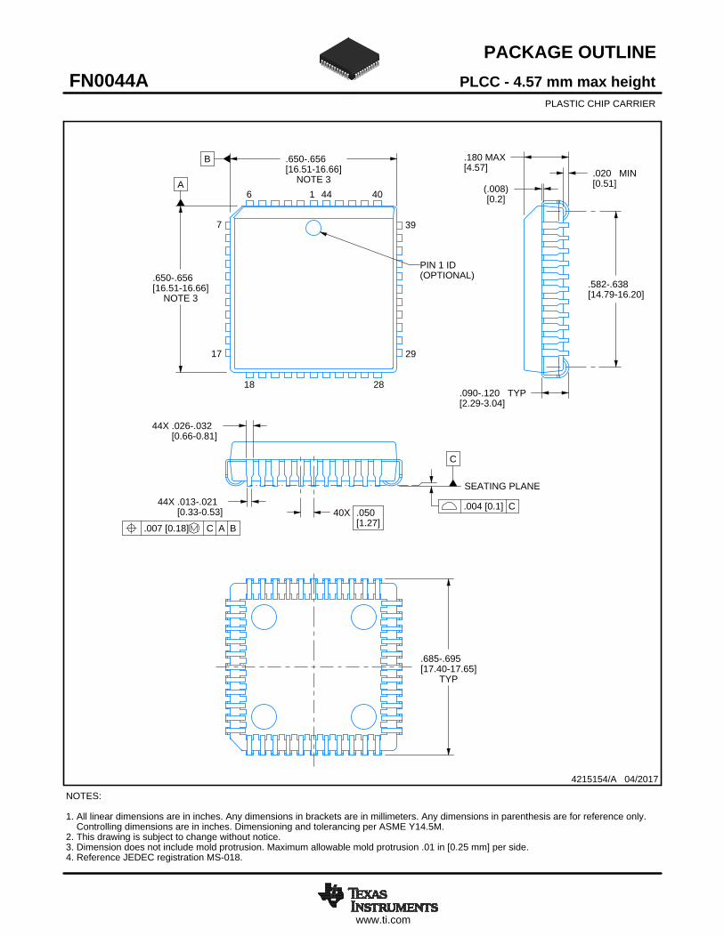
PACKAGE OUTLINE
C
44X -.021.013-0.530.33[ ]
44X -.032.026-0.810.66[ ]
TYP
-.695.685-17.6517.40[ ]
40X .050[1.27]
-.638.582-16.2014.79[ ]
.020 MIN[0.51]
TYP-.120.090-3.042.29[ ]
.180 MAX[4.57]
B
NOTE 3
-.656.650-16.6616.51[ ]
A
NOTE 3
-.656.650-16.6616.51[ ]
(.008)[0.2]
4215154/A 04/2017
4215154/A 04/2017
PLCC - 4.57 mm max heightFN0044APLASTIC CHIP CARRIER
NOTES: 1. All linear dimensions are in inches. Any dimensions in brackets are in millimeters. Any dimensions in parenthesis are for reference only. Controlling dimensions are in inches. Dimensioning and tolerancing per ASME Y14.5M. 2. This drawing is subject to change without notice.3. Dimension does not include mold protrusion. Maximum allowable mold protrusion .01 in [0.25 mm] per side.4. Reference JEDEC registration MS-018.
PIN 1 ID(OPTIONAL)
1 446
18 28
29
39
40
7
17
.004 [0.1] C
.007 [0.18] C A B
SEATING PLANE
SCALE 0.800

www.ti.com
EXAMPLE BOARD LAYOUT
.002 MAX[0.05]
ALL AROUND
.002 MIN[0.05]
ALL AROUND
44X (.093 )[2.35]
44X (.030 )[0.75]
40X (.050 )[1.27]
(.64 )[16.2]
(.64 )[16.2]
(R.002 ) TYP[0.05]
4215154/A 04/2017
4215154/A 04/2017
PLCC - 4.57 mm max heightFN0044APLASTIC CHIP CARRIER
NOTES: (continued) 5. Publication IPC-7351 may have alternate designs.6. Solder mask tolerances between and around signal pads can vary based on board fabrication site.
LAND PATTERN EXAMPLEEXPOSED METAL SHOWN
SCALE:4X
SYMM
SYMM
1 446
18 28
29
39
40
7
17
METAL SOLDER MASKOPENING
NON SOLDER MASKDEFINED
(PREFERRED)
SOLDER MASK DETAILS
EXPOSED METAL
SOLDER MASKOPENING
METAL UNDERSOLDER MASK
SOLDER MASKDEFINED
EXPOSED METAL

www.ti.com
EXAMPLE STENCIL DESIGN
44X (.030 )[0.75]
44X (.093 )[2.35]
(.64 )[16.2]
(.64 )[16.2]
40X (.050 )[1.27]
(R.002 ) TYP[0.05]
PLCC - 4.57 mm max heightFN0044APLASTIC CHIP CARRIER
4215154/A 04/2017
PLCC - 4.57 mm max heightFN0044APLASTIC CHIP CARRIER
NOTES: (continued) 7. Laser cutting apertures with trapezoidal walls and rounded corners may offer better paste release. IPC-7525 may have alternate design recommendations.8. Board assembly site may have different recommendations for stencil design.
SOLDER PASTE EXAMPLEBASED ON 0.125 mm THICK STENCIL
SCALE:4X
SYMM
SYMM
1 446
18 28
29
39
40
7
17

IMPORTANT NOTICE AND DISCLAIMERTI PROVIDES TECHNICAL AND RELIABILITY DATA (INCLUDING DATASHEETS), DESIGN RESOURCES (INCLUDING REFERENCEDESIGNS), APPLICATION OR OTHER DESIGN ADVICE, WEB TOOLS, SAFETY INFORMATION, AND OTHER RESOURCES “AS IS”AND WITH ALL FAULTS, AND DISCLAIMS ALL WARRANTIES, EXPRESS AND IMPLIED, INCLUDING WITHOUT LIMITATION ANYIMPLIED WARRANTIES OF MERCHANTABILITY, FITNESS FOR A PARTICULAR PURPOSE OR NON-INFRINGEMENT OF THIRDPARTY INTELLECTUAL PROPERTY RIGHTS.These resources are intended for skilled developers designing with TI products. You are solely responsible for (1) selecting the appropriateTI products for your application, (2) designing, validating and testing your application, and (3) ensuring your application meets applicablestandards, and any other safety, security, or other requirements. These resources are subject to change without notice. TI grants youpermission to use these resources only for development of an application that uses the TI products described in the resource. Otherreproduction and display of these resources is prohibited. No license is granted to any other TI intellectual property right or to any third partyintellectual property right. TI disclaims responsibility for, and you will fully indemnify TI and its representatives against, any claims, damages,costs, losses, and liabilities arising out of your use of these resources.TI’s products are provided subject to TI’s Terms of Sale (https:www.ti.com/legal/termsofsale.html) or other applicable terms available eitheron ti.com or provided in conjunction with such TI products. TI’s provision of these resources does not expand or otherwise alter TI’sapplicable warranties or warranty disclaimers for TI products.IMPORTANT NOTICE
Mailing Address: Texas Instruments, Post Office Box 655303, Dallas, Texas 75265Copyright © 2021, Texas Instruments Incorporated


![CAN bus Data Stream Wrapper - DiVA portal1095657/FULLTEXT01.pdf · The Controller Area Network (CAN) bus [3] is a vehicle bus standard designed to allow micro-controllers and devices](https://static.fdocuments.us/doc/165x107/5e9af5e106ccb7365b4c3227/can-bus-data-stream-wrapper-diva-1095657fulltext01pdf-the-controller-area.jpg)