SMSC USB3320 vs TUSB1210 - Texas...
15
TI Confidential – NDA Restrictions SMSC USB3320 vs TUSB1210 Ver1.2 28July 2010 TUSB1210 Overview : • TUSB1210 is TI’s first single-chip stand-alone USB2.0 HS transceiver chip with ULPI interface, and master/slave mode clock capability allowing it to be seamlessly connected with OMAP24xx and OMAP 34xx application processors or any other ULPI-interface USB2.0 HS controller device. • TUSB1210 is available in a 32QFN package, and sampling soon !! • TUSB1210 was designed to be pin-to-pin compatible with SMSC USB3320 device. • However TUSB1210 is not a drop-in replacement for SMSC USB3320, some minor changes are required • To allow a single application board to be capable of using both devices it is recommended to follow the guidelines in the following slides • Both devices are compared for: – Block Diagram – Pinout – Application Diagram 1. ULPI input clock mode 2. ULPI output clock mode (REFCLK = 26MHz) 3. ULPI output clock mode (REFCLK = 19.2MHz) – Package Create PDF files without this message by purchasing novaPDF printer (http://www.novapdf.com)
Transcript of SMSC USB3320 vs TUSB1210 - Texas...

TI Confidential – NDA Restrictions
SMSC USB3320 vs TUSB1210 Ver1.2 28July 2010
TUSB1210 Overview :• TUSB1210 is TI’s first single-chip stand-alone USB2.0 HS transceiver chip with ULPI interface,
and master/slave mode clock capability allowing it to be seamlessly connected with OMAP24xx and OMAP 34xx application processors or any other ULPI-interface USB2.0 HS controllerdevice.
• TUSB1210 is available in a 32QFN package, and sampling soon !! • TUSB1210 was designed to be pin-to-pin compatible with SMSC USB3320 device. • However TUSB1210 is not a drop-in replacement for SMSC USB3320, some minor changes
are required• To allow a single application board to be capable of using both devices it is recommended to
follow the guidelines in the following slides• Both devices are compared for:
– Block Diagram– Pinout– Application Diagram
1. ULPI input clock mode2. ULPI output clock mode (REFCLK = 26MHz)3. ULPI output clock mode (REFCLK = 19.2MHz)
– Package
Create PDF files without this message by purchasing novaPDF printer (http://www.novapdf.com)

TI Confidential – NDA Restrictions
SMSC3320 vs TUSB1210: Block Diagram
TUSB1210
USB-IP
OTG
1V5
3V3
1V8
PORVBAT
PLL
PHYANA
PHYDIG
+ULPI
+REGS
32KSLICER
EEPROM
BGAP& REF
PORDIG
DIG
OTG_D
JTAG
TRIM
PWR FSM
PORVIO
CTRL
RST_DIG
VDDIO (32)
VBAT (21)
N/C (24)
VDD15 (12)
VDD18 (28)VDD33 (20)
DP (18)DM (19)
ID (23)
(22) VBUS
( 1) REFCLK(25) N/C
(17) CPEN
(3:7,9:10,13) D
ATA
(7:0)(2 ) N
XT(31) D
IR(29) STP(26) C
LOC
K
(16) N/C(15) N/C
VDD18 (30)
PKG Substrate (Ground)
(14) CFG(11) CS( 8) N/C
(27) RESETB
SMSC USB3320
Create PDF files without this message by purchasing novaPDF printer (http://www.novapdf.com)
TI Confidential – NDA Restrictions
SMSC3320 vs TUSB1210 : Pinout
PIN # SMSC USB 3320 TUSB1210 COMMENT
1 CLKOUT REFCLK To match SMSC ULPI input mode. Tie to VDDIO in ULPI input clock mode
8 REFSEL0 N/C Not bonded. Only 19.2M/26M input frequencies supported, via CFG pin #14..
11 REFSEL1 CS
Active-high chip select pin. When low the IC is in power down and ULPI bus is tri-stated. When high normal operation. Tie to VDDIO if unused.
12 N/C VDD15 Bypass capacitor required on this pin for internal VDD15 LDO stability.
14 REFSEL2 CFG REFCLK input frequency is 26M when this bit is '1' else 19.2MHz.
15 SPK_L N/C High-impedance (test pin). Audio switch feature not supported.
16 SPK_R N/C Not bonded. Audio switch feature not supported.
25 XO N/C XTAL Oscillator not supported
26 REFCLK CLOCK CLOCK pin placed at pin#26 to match SMSC ULPI input mode. Connect to 60MHz clock output pin of Link.
VD
DIO
DIR
VD
D1
8
ST
P
VD
D1
8
RE
SET
B
CLO
CK
N/
C
32
31
30
29
28
27
26
25
REFCLK 1 24 N/CNXT 2 23 ID
DATA0 3 TUSB1210 22 VBUSDATA1 4 32-pin QFN 21 VBATDATA2 5 20 VDD33DATA3 6 19 DMDATA4 7 GND 18 DP
N/C 8 17 CPEN
9 10
11
12
13
14
15
16
DA
TA
5
DA
TA
6
CS
VD
D1
5
DA
TA
7
CFG
N/
C
N/
C
SMSC USB3320
Create PDF files without this message by purchasing novaPDF printer (http://www.novapdf.com)
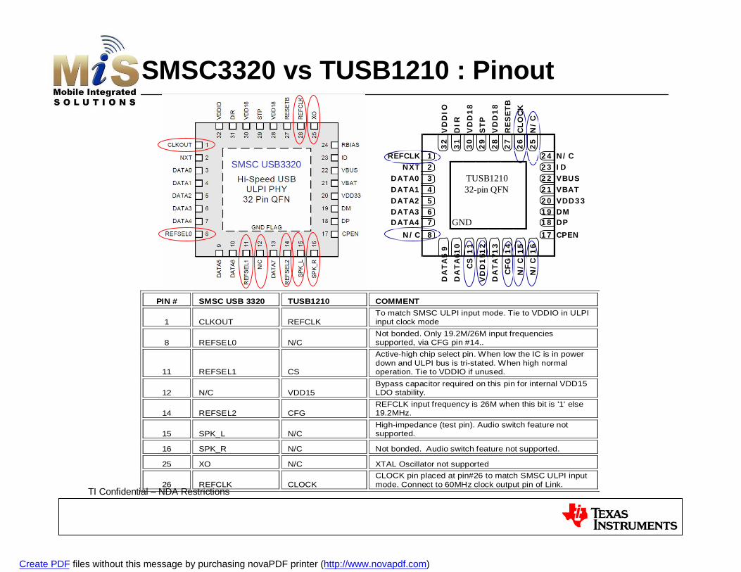
TI Confidential – NDA Restrictions
Suggested Application Diagram : TUSB1210 ULPI Input Clock Mode
Suggested Application Diagram for compatibility with OMAP3 (Host or OTG, ULPI input-clock mode)
RESETB
DATA7DATA6DATA5DATA4DATA3DATA2DATA1DATA0
STPNXTDIR
REFCLK
N/C
CLOCK
VDDIO
VDD18
N/CGND
CFGCSN/C
CPEN
VBUS
VBAT
VDD33
ID
DM
DP
N/CN/C
VDDIO Supply
3.1~5.5VSupply
VDDIO Supply
1.8V Supply
RESETB
DATA7DATA6DATA5DATA4DATA3DATA2DATA1DATA0STPNXTDIRCLOCK
TUSB1210
OptionalSignals
to DP/DM
USBReceptacle
ID
DM
DPSHIELD
GND
VBUS
5VOUT
ENIN
VBUS Switch
LinkController
TUSB1210: V1.2 17MAR 2010Pin11 (CS) must be tied high.Pin14 (CFG) tie-high is don’t care since ULPI clock is used in input modePin8 (N/C) tie-high is don’t care since non-connected internally
Ext 3V supply
supported
CVBUS CVDD33
CBYP
CVDD18
CVDDIO
Open
Short
VDD15CVDD15
14118
17
12
22
21
20
23
19
18
15
16
27
1310976543292311
25
26
32
28,30
24
Short
ESD
Open
Pin1 (REFCLK)) must be tied low.
1A
Create PDF files without this message by purchasing novaPDF printer (http://www.novapdf.com)

TI Confidential – NDA Restrictions
Suggested Application Diagram : SMSC USB3320ULPI Input Clock Mode
Suggested Application Diagram for compatibility with OMAP3 (Host or OTG, ULPI input-clock mode)
RESETB
DATA7DATA6DATA5DATA4DATA3DATA2DATA1DATA0
STPNXTDIR
CLKOUT
XO
REFCLK
VDDIO
VDD18
RBIASGND
REFSEL2REFSEL1REFSEL0
CPEN
VBUS
VBAT
VDD33
ID
DM
DP
SPK_LSPK_R
VDDIO Supply
3.1~5.5VSupply
VDDIO Supply
1.8V Supply
RESETB
DATA7DATA6DATA5DATA4DATA3DATA2DATA1DATA0STPNXTDIRCLOCK
SMSC USB3320
OptionalSignals
to DP/DM
USBReceptacle
ID
DM
DPSHIELD
GND
VBUS
5VOUT
ENIN
VBUS Switch
LinkController
Ext 3V supply
supported
CVBUS COUT
CBYP
CBYP
CBYP
RBIAS
Open
Open
RVBUS
Taken from SMSC USB3320 spec Rev0.5 available on web (ULPI clock input mode)
1411
8
17
22
21
20
23
19
18
15
16
27
1310976543292311
25
26
32
28,30
24
N/CCVDD15
12
Open
SMSC USB3320 17MAR 2010
1B
Create PDF files without this message by purchasing novaPDF printer (http://www.novapdf.com)

TI Confidential – NDA Restrictions
TUSB1210/SMSC USB3320 Connection rulesULPI Input Clock Mode
• TUSB1210 – Clock connection:
• Slave mode clock (ULPI clock input from LINK): – Pin1 (REFCLK) 0-ohm to GND– Pin26 (CLOCK) <- LINK ULPI CLKOUT
– Pin12 (VDD15) 0-ohm to CVDD15 (2.2uF)– Pin22 (VBUS) 0-ohm series resistor– Pin24(NC) open
• SMSC USB3320 – Note Pin numbers and physical package pin positions are same as TUSB1210 (but
pin names differ)– Clock Connection:
• Slave mode clock (ULPI clock output to LINK): – Pin1 (CLKOUT) 0-ohm to VDDIO– Pin26 (REFCLK) <- LINK ULPI CLKOUT
– Pin12 (NC) open– Pin22 (VBUS) RVBUS 10kohm 5% for HOST device, 1kohm 5% resistor for OTG
device – Pin24 (RBIAS) RBIAS 8.06kohm +/-1%
1C
Create PDF files without this message by purchasing novaPDF printer (http://www.novapdf.com)

TI Confidential – NDA Restrictions
Suggested Application Diagram : TUSB1210ULPI Output Clock Mode (REFCLK 26MHz)
Suggested Application Diagram for compatibility with OMAP3 (Device, ULPI output-clock mode)
2A
Create PDF files without this message by purchasing novaPDF printer (http://www.novapdf.com)

TI Confidential – NDA Restrictions
Suggested Application Diagram for compatibility with OMAP3 (Device, ULPI output-clock mode)
2B
RESETB
DATA7DATA6DATA5DATA4DATA3DATA2DATA1DATA0
STPNXTDIR
CLKOUT
XO
REFCLK
VDDIO
VDD18
RBIASGND
REFSEL2REFSEL1REFSEL0
CPEN
VBUS
VBAT
VDD33
ID
DM
DP
SPK_LSPK_R
VDDIO Supply
3.1~5.5VSupply
VDDIO Supply
1.8V Supply
SMSC USB3320
OptionalSignals
to DP/DM
USBReceptacle
DM
DPSHIELD
GND
VBUSExt 3V supply
supported
CVBUS COUT
CBYP
CBYP
CBYP
RBIAS
Open
Open
RVBUS
Taken from SMSC USB3320 spec Rev0.5 available on web (ULPI clock output mode) REFCLK 26MHz
1411
8
17
22
21
20
23
19
18
15
16
27
1310976543292311
25
26
32
28,30
24
N/CCVDD15
12
Open
SMSC USB3320 28JUL 2010
DATA7DATA6DATA5DATA4DATA3DATA2DATA1DATA0STPNXTDIRCLKIN
LinkController
RESETB
REFCLK
Suggested Application Diagram : SMSC USB3320ULPI Output Clock Mode (REFCLK 26MHz)
Create PDF files without this message by purchasing novaPDF printer (http://www.novapdf.com)

TI Confidential – NDA Restrictions
TUSB1210/SMSC USB3320 Connection rulesULPI Output Clock Mode (REFCLK 26MHz)
• TUSB1210 – Clock connection:
• Master mode clock (ULPI clock output to Link): – Note: TUSB1210 Pin1 (REFCLK) input level must be 3.3V (square-wave). May require Level Shifter – Pin1 (REFCLK) <- LINK REFCLK– Pin26 (CLOCK) -> LINK ULPI CLKIN
– Pin12 (VDD15) 0-ohm to CVDD15 (2.2uF)– Pin22 (VBUS) 0-ohm series resistor– Pin24(NC) open
• SMSC USB3320 – Note Pin numbers and physical package pin positions are same as TUSB1210 (but pin
names differ)– Clock Connection:
• Master mode clock: (ULPI clock output to LINK): – Pin1 (CLKOUT) -> LINK ULPI CLKIN– Pin26 (REFCLK) <- LINK REFCLK
– Pin12 (NC) open– Pin22 (VBUS) RVBUS 10kohm 5% for HOST device, 1kohm 5% resistor for OTG
device – Pin24 (RBIAS) RBIAS 8.06kohm +/-1%
2C
Create PDF files without this message by purchasing novaPDF printer (http://www.novapdf.com)

TI Confidential – NDA Restrictions
Suggested Application Diagram : TUSB1210ULPI Output Clock Mode (REFCLK 19.2MHz)
Suggested Application Diagram for compatibility with OMAP3 (Device, ULPI output-clock mode)
3A
Create PDF files without this message by purchasing novaPDF printer (http://www.novapdf.com)

TI Confidential – NDA Restrictions
Suggested Application Diagram for compatibility with OMAP3 (Device, ULPI output-clock mode)
3B
RESETB
DATA7DATA6DATA5DATA4DATA3DATA2DATA1DATA0
STPNXTDIR
CLKOUT
XO
REFCLK
VDDIO
VDD18
RBIASGND
REFSEL2REFSEL1REFSEL0
CPEN
VBUS
VBAT
VDD33
ID
DM
DP
SPK_LSPK_R
3.1~5.5VSupply
VDDIO Supply
1.8V Supply
SMSC USB3320
OptionalSignals
to DP/DM
USBReceptacle
DM
DPSHIELD
GND
VBUSExt 3V supply
supported
CVBUS COUT
CBYP
CBYP
CBYP
RBIAS
Open
Open
RVBUS
Taken from SMSC USB3320 spec Rev0.5 available on web (ULPI clock output mode) REFCLK 19.2MHz
1411
8
17
22
21
20
23
19
18
15
16
27
1310976543292311
25
26
32
28,30
24
N/CCVDD15
12
Open
SMSC USB3320 17MAR 2010
DATA7DATA6DATA5DATA4DATA3DATA2DATA1DATA0STPNXTDIRCLKIN
LinkController
RESETB
REFCLK
VDDIO Supply
Suggested Application Diagram : SMSC USB3320ULPI Output Clock Mode (REFCLK 19.2MHz)
Create PDF files without this message by purchasing novaPDF printer (http://www.novapdf.com)

TI Confidential – NDA Restrictions
TUSB1210/SMSC USB3320 Connection rulesULPI Output Clock Mode (REFCLK 19.2MHz)
• TUSB1210 – Clock connection:
• Master mode clock (ULPI clock output to Link): – Note: TUSB1210 Pin1 (REFCLK) input level must be 3.3V (square-wave). May require Level Shifter – Pin1 (REFCLK) <- LINK REFCLK– Pin26 (CLOCK) -> LINK ULPI CLKIN
– Pin11(CS) 0-ohm to VDDIO– Pin14(CFG) 0-ohm to GND– Pin12 (VDD15) 0-ohm to CVDD15 (2.2uF)– Pin22 (VBUS) 0-ohm series resistor– Pin24(NC) open
• SMSC USB3320 – Note Pin numbers and physical package pin positions are same as TUSB1210 (but pin names differ)– Clock Connection:
• Master mode clock: (ULPI clock output to LINK): – Pin1 (CLKOUT) -> LINK ULPI CLKIN– Pin26 (REFCLK) <- LINK REFCLK
– Pin11(REFSEL1) 0-ohm to GND– Pin14(REFSEL2) 0-ohm to VDDIO– Pin12 (NC) open– Pin22 (VBUS) RVBUS 10kohm 5% for HOST device, 1kohm 5% resistor for OTG device – Pin24 (RBIAS) RBIAS 8.06kohm +/-1%
3C
Create PDF files without this message by purchasing novaPDF printer (http://www.novapdf.com)

TI Confidential – NDA Restrictions
TUSB1210 External Components Summary
• Excerpt from TUSB1210 Datasheet (*)(*) This is intended for reference only, the TUSB1210 datasheet is the official information source
Create PDF files without this message by purchasing novaPDF printer (http://www.novapdf.com)
TI Confidential – NDA Restrictions
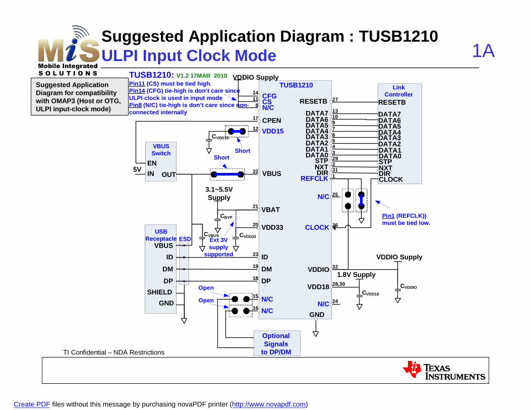
Package : TUSB1210
• Package:– QFN 32-pin– 5 x 5– 0.5mm pitch
Create PDF files without this message by purchasing novaPDF printer (http://www.novapdf.com)

TI Confidential – NDA Restrictions
Package : SMSC USB3320
Create PDF files without this message by purchasing novaPDF printer (http://www.novapdf.com)