
TUSB1210-Q1 Standalone USB Transceiver Chip … Folder Sample & Buy Technical Documents Tools &...
66
Product Folder Sample & Buy Technical Documents Tools & Software Support & Community TUSB1210-Q1 SLLSEL4A – SEPTEMBER 2014 – REVISED OCTOBER 2014 TUSB1210-Q1 Standalone USB Transceiver Chip Silicon 1 Features 3 Description The TUSB1210-Q1 is a USB2.0 transceiver chip, 1• AEC-Q100 Qualified with: designed to interface with a USB controller via a ULPI – Temperature Grade 3: –40°C to 85°C interface. It supports all USB2.0 data rates (High- – HBM ESD Classification 1C Speed 480 Mbps, Full-Speed 12 Mbps and Low- Speed 1.5 Mbps), and is compliant to both Host and – CDM ESD Classification C4B Peripheral modes. It additionally supports a UART • USB2.0 PHY Transceiver Chip, Designed to mode and legacy ULPI serial modes. Interface with a USB Controller via a ULPI 12-pin TUSB1210-Q1 also supports the OTG (Ver1.3) Interface, Fully Compliant With: optional addendum to the USB 2.0 Specification, – Universal Serial Bus Specification Rev. 2.0 including Host Negotiation Protocol (HNP) and – On-The-Go Supplement to the USB 2.0 Session Request Protocol (SRP). Specification Rev. 1.3 The DP/DM external component compensation in the – UTMI+ Low Pin Interface (ULPI) Specification transmitter compensates for variations in the series Rev. 1.1 impendence in order to match with the data line • DP/DM Line External Component Compensation impedance and the receiver input impedance, to limit data reflections, and thereby, improve eye diagrams. (Patent #US7965100 B1) • Interfaces to Host, Peripheral and OTG Device Device Information (1) Cores; Optimized for Portable Devices or System PART NUMBER PACKAGE BODY SIZE (NOM) ASICs with Built-in USB OTG Device Core TUSB1210-Q1 VQFN (32) 5.00 mm x 5.00 mm • Complete USB OTG Physical Front-End that (1) For all available packages, see the orderable addendum at Supports Host Negotiation Protocol (HNP) and the end of the datasheet. Session Request Protocol (SRP) • ULPI Interface: Diagram – I/O Interface (1.8 V) Optimized for Non- Terminated 50 Ω Line Impedance – ULPI CLOCK Pin (60 MHz) Supports Both Input and Output Clock Configurations – Fully Programmable ULPI-Compliant Register Set • Available in a 32-Pin Quad Flat No Lead [QFN (RHB)] Package 2 Applications • Mobile Phones • Tablet Devices • Desktop Computers • Portable Computers • Video Game Consoles • Portable Music Players 1 An IMPORTANT NOTICE at the end of this data sheet addresses availability, warranty, changes, use in safety-critical applications, intellectual property matters and other important disclaimers. PRODUCTION DATA.
Transcript of TUSB1210-Q1 Standalone USB Transceiver Chip … Folder Sample & Buy Technical Documents Tools &...
Product
Folder
Sample &Buy
Technical
Documents
Tools &
Software
Support &Community
TUSB1210-Q1SLLSEL4A –SEPTEMBER 2014–REVISED OCTOBER 2014
TUSB1210-Q1 Standalone USB Transceiver Chip Silicon1 Features 3 Description
The TUSB1210-Q1 is a USB2.0 transceiver chip,1• AEC-Q100 Qualified with:
designed to interface with a USB controller via a ULPI– Temperature Grade 3: –40°C to 85°C interface. It supports all USB2.0 data rates (High-– HBM ESD Classification 1C Speed 480 Mbps, Full-Speed 12 Mbps and Low-
Speed 1.5 Mbps), and is compliant to both Host and– CDM ESD Classification C4BPeripheral modes. It additionally supports a UART• USB2.0 PHY Transceiver Chip, Designed to mode and legacy ULPI serial modes.Interface with a USB Controller via a ULPI 12-pinTUSB1210-Q1 also supports the OTG (Ver1.3)Interface, Fully Compliant With:optional addendum to the USB 2.0 Specification,– Universal Serial Bus Specification Rev. 2.0 including Host Negotiation Protocol (HNP) and
– On-The-Go Supplement to the USB 2.0 Session Request Protocol (SRP).Specification Rev. 1.3
The DP/DM external component compensation in the– UTMI+ Low Pin Interface (ULPI) Specification transmitter compensates for variations in the series
Rev. 1.1 impendence in order to match with the data line• DP/DM Line External Component Compensation impedance and the receiver input impedance, to limit
data reflections, and thereby, improve eye diagrams.(Patent #US7965100 B1)• Interfaces to Host, Peripheral and OTG Device Device Information(1)
Cores; Optimized for Portable Devices or SystemPART NUMBER PACKAGE BODY SIZE (NOM)ASICs with Built-in USB OTG Device Core
TUSB1210-Q1 VQFN (32) 5.00 mm x 5.00 mm• Complete USB OTG Physical Front-End that(1) For all available packages, see the orderable addendum atSupports Host Negotiation Protocol (HNP) and
the end of the datasheet.Session Request Protocol (SRP)• ULPI Interface: Diagram
– I/O Interface (1.8 V) Optimized for Non-Terminated 50 Ω Line Impedance
– ULPI CLOCK Pin (60 MHz) Supports BothInput and Output Clock Configurations
– Fully Programmable ULPI-Compliant RegisterSet
• Available in a 32-Pin Quad Flat No Lead[QFN (RHB)] Package
2 Applications• Mobile Phones• Tablet Devices• Desktop Computers• Portable Computers• Video Game Consoles• Portable Music Players
1
An IMPORTANT NOTICE at the end of this data sheet addresses availability, warranty, changes, use in safety-critical applications,intellectual property matters and other important disclaimers. PRODUCTION DATA.
TUSB1210-Q1SLLSEL4A –SEPTEMBER 2014–REVISED OCTOBER 2014 www.ti.com
Table of Contents7.4 Device Functional Modes........................................ 181 Features .................................................................. 17.5 Register Map........................................................... 202 Applications ........................................................... 1
8 Application and Implementation ........................ 493 Description ............................................................. 18.1 Application Information............................................ 494 Revision History..................................................... 28.2 Typical Application .................................................. 495 Pin Configuration and Functions ......................... 38.3 External Components.............................................. 536 Specifications......................................................... 4
9 Power Supply Recommendations ...................... 546.1 Absolute Maximum Ratings ...................................... 49.1 TUSB1210 Power Supply ....................................... 546.2 Handling Ratings....................................................... 49.2 Ground .................................................................... 546.3 Recommended Operating Conditions....................... 59.3 Power Providers...................................................... 546.4 Thermal Information .................................................. 59.4 Power Modules ....................................................... 546.5 Analog I/O Electrical Characteristics ........................ 59.5 Power Consumption................................................ 556.6 Digital I/O Electrical Characteristics.......................... 5
10 Layout................................................................... 566.7 Digital IO Pins (Non-ULPI) ....................................... 510.1 Layout Guidelines ................................................. 566.8 PHY Electrical Characteristics .................................. 610.2 Layout Example .................................................... 566.9 Pullup/Pulldown Resistors......................................... 8
11 Device and Documentation Support ................. 576.10 OTG Electrical Characteristics................................ 911.1 Documentation Support ........................................ 576.11 Power Characteristics ........................................... 1011.2 Community Resources.......................................... 576.12 Switching Characteristics ...................................... 1011.3 Trademarks ........................................................... 576.13 Timing Requirements ............................................ 1111.4 Electrostatic Discharge Caution............................ 576.14 Typical Characteristics .......................................... 1311.5 Glossary ................................................................ 577 Detailed Description ............................................ 14
12 Mechanical, Packaging, and Orderable7.1 Overview ................................................................. 14Information ........................................................... 587.2 Functional Block Diagram ....................................... 1412.1 Via Channel........................................................... 587.3 Feature Description................................................. 1512.2 Packaging Information .......................................... 58
4 Revision History
Changes from Original (September 2014) to Revision A Page
• Changed the Features list ..................................................................................................................................................... 1• Deleted 5 paragraphs from the Description following: "TUSB1210-Q1 also supports the OTG (Ver1.3).."........................... 1• Changed the Diagram image.................................................................................................................................................. 1• Added VIL and VIH to the Recommended Operating Conditions table .................................................................................. 5• Changed the Thermal Information table ................................................................................................................................ 5• Changed the Digital I/O Electrical Characteristics table ........................................................................................................ 5• Digital IO Electrical Characteristics sections to the Switching Characteristics..................................................................... 10• Added the Typical Characteristics section............................................................................................................................ 13• Added 5 new paragraphs to the Overview section............................................................................................................... 14
2 Submit Documentation Feedback Copyright © 2014, Texas Instruments Incorporated
Product Folder Links: TUSB1210-Q1

VD
DIO
DIR
VD
D18
ST
P
VD
D18
RE
SE
TB
CLO
CK
N/C
32
31
30
29
28
27
26
25
REFCLK 1 24 N/C
NXT 2 23 ID
DATA0 3 22 VBUS
DATA1 4 21 VBAT
DATA2 5 20 VDD33
DATA3 6 19 DM
DATA4 7 GND 18 DP
N/C 8 17 CPEN
9
10
11
12
13
14
15
16
DA
TA
5
DA
TA
6
CS
VD
D15
DA
TA
7
CF
G
N/C
N/C
TUSB1210-Q1www.ti.com SLLSEL4A –SEPTEMBER 2014–REVISED OCTOBER 2014
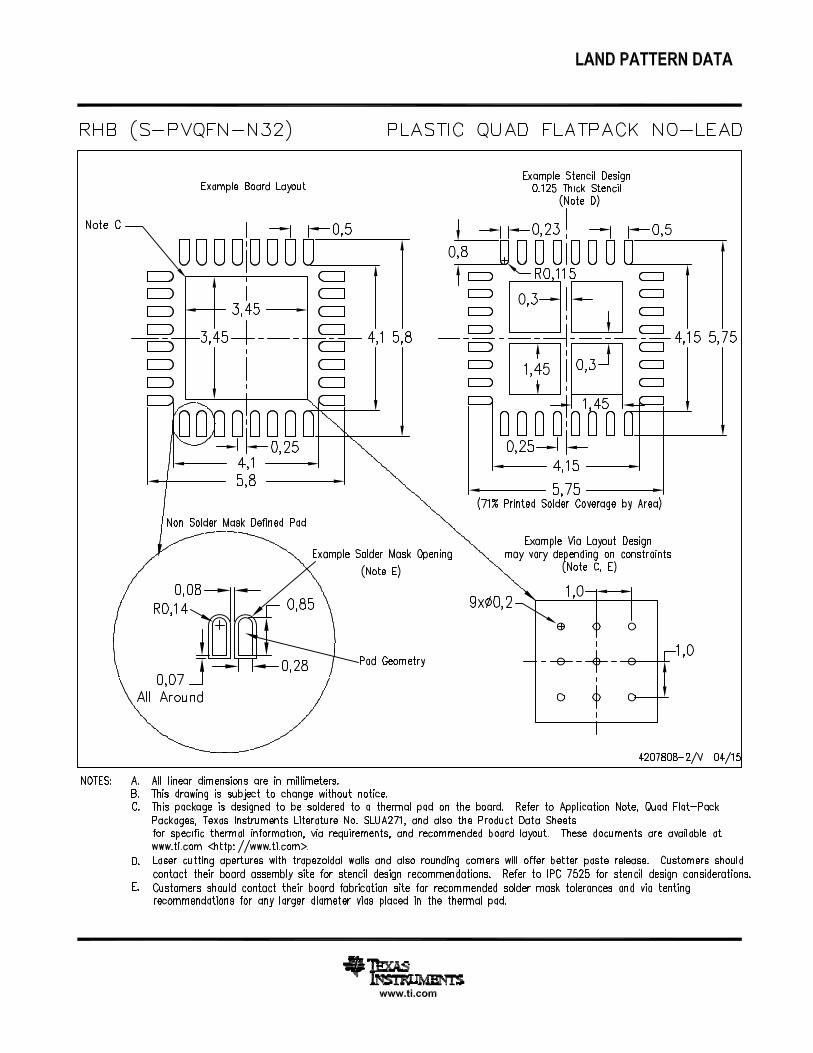
5 Pin Configuration and Functions
RHB PackageTop View
Pin FunctionsPIN
A/D TYPE LEVEL DESCRIPTIONNAME NO.
REFCLK clock frequency configuration pin. Two frequencies are supported: 19.2 MHzCFG 14 D I VDDIO when 0, or 26 MHz when 1.
ULPI 60 MHz clock on which ULPI data is synchronized.
Two modes are possible:CLOCK 26 D O VDDIO Input Mode: CLOCK defaults as an input.
Output Mode: When an input clock is detected on REFCLK pin (after 4rising edges) then CLOCK will change to an output.
CPEN 17 D O VDD33 CMOS active-high digital output control of external 5V VBUS supply
Active-high chip select pin. When low the IC is in power down and ULPI bus is tri-CS 11 D I VDDIO stated. When high normal operation. Tie to VDDIO if unused.
DATA0 3 D I/O VDDIO ULPI DATA input/output signal 0 synchronized to CLOCK
DATA1 4 D I/O VDDIO ULPI DATA input/output signal 1 synchronized to CLOCK
DATA2 5 D I/O VDDIO ULPI DATA input/output signal 2 synchronized to CLOCK
DATA3 6 D I/O VDDIO ULPI DATA input/output signal 3 synchronized to CLOCK
DATA4 7 D I/O VDDIO ULPI DATA input/output signal 4 synchronized to CLOCK
DATA5 9 D I/O VDDIO ULPI DATA input/output signal 5 synchronized to CLOCK
DATA6 10 D I/O VDDIO ULPI DATA input/output signal 6 synchronized to CLOCK
DATA7 13 D I/O VDDIO ULPI DATA input/output signal 7 synchronized to CLOCK
DIR 31 D O VDDIO ULPI DIR output signal
DM 19 A I/O VDD33 DM pin of the USB connector
DP 18 A I/O VDD33 DP pin of the USB connector
ID 23 A I/O VDD33 Identification (ID) pin of the USB connector
N/C 8 – – VDDIO No connect
15,16, 24,N/C – – – No connect24
NXT 2 D O VDDIO ULPI NXT output signal
Copyright © 2014, Texas Instruments Incorporated Submit Documentation Feedback 3
Product Folder Links: TUSB1210-Q1
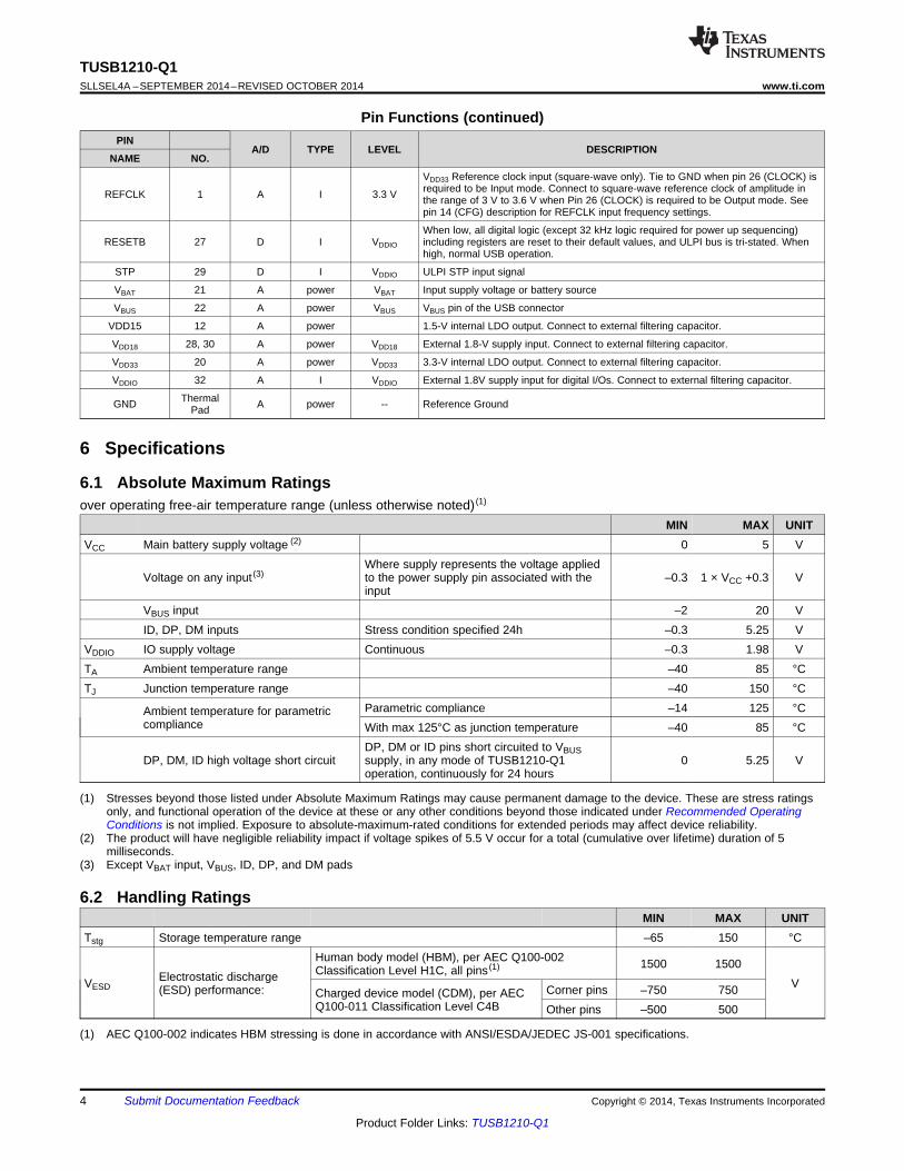
TUSB1210-Q1SLLSEL4A –SEPTEMBER 2014–REVISED OCTOBER 2014 www.ti.com
Pin Functions (continued)PIN
A/D TYPE LEVEL DESCRIPTIONNAME NO.
VDD33 Reference clock input (square-wave only). Tie to GND when pin 26 (CLOCK) isrequired to be Input mode. Connect to square-wave reference clock of amplitude inREFCLK 1 A I 3.3 V the range of 3 V to 3.6 V when Pin 26 (CLOCK) is required to be Output mode. Seepin 14 (CFG) description for REFCLK input frequency settings.
When low, all digital logic (except 32 kHz logic required for power up sequencing)RESETB 27 D I VDDIO including registers are reset to their default values, and ULPI bus is tri-stated. When
high, normal USB operation.
STP 29 D I VDDIO ULPI STP input signal
VBAT 21 A power VBAT Input supply voltage or battery source
VBUS 22 A power VBUS VBUS pin of the USB connector
VDD15 12 A power 1.5-V internal LDO output. Connect to external filtering capacitor.
VDD18 28, 30 A power VDD18 External 1.8-V supply input. Connect to external filtering capacitor.
VDD33 20 A power VDD33 3.3-V internal LDO output. Connect to external filtering capacitor.
VDDIO 32 A I VDDIO External 1.8V supply input for digital I/Os. Connect to external filtering capacitor.
ThermalGND A power -- Reference GroundPad
6 Specifications
6.1 Absolute Maximum Ratingsover operating free-air temperature range (unless otherwise noted) (1)
MIN MAX UNITVCC Main battery supply voltage (2) 0 5 V
Where supply represents the voltage appliedVoltage on any input (3) to the power supply pin associated with the –0.3 1 × VCC +0.3 V
inputVBUS input –2 20 VID, DP, DM inputs Stress condition specified 24h –0.3 5.25 V
VDDIO IO supply voltage Continuous –0.3 1.98 VTA Ambient temperature range –40 85 °CTJ Junction temperature range –40 150 °C
Parametric compliance –14 125 °CAmbient temperature for parametriccompliance With max 125°C as junction temperature –40 85 °C
DP, DM or ID pins short circuited to VBUSDP, DM, ID high voltage short circuit supply, in any mode of TUSB1210-Q1 0 5.25 V
operation, continuously for 24 hours
(1) Stresses beyond those listed under Absolute Maximum Ratings may cause permanent damage to the device. These are stress ratingsonly, and functional operation of the device at these or any other conditions beyond those indicated under Recommended OperatingConditions is not implied. Exposure to absolute-maximum-rated conditions for extended periods may affect device reliability.
(2) The product will have negligible reliability impact if voltage spikes of 5.5 V occur for a total (cumulative over lifetime) duration of 5milliseconds.
(3) Except VBAT input, VBUS, ID, DP, and DM pads
6.2 Handling RatingsMIN MAX UNIT
Tstg Storage temperature range –65 150 °CHuman body model (HBM), per AEC Q100-002 1500 1500Classification Level H1C, all pins (1)
Electrostatic dischargeVESD V(ESD) performance: Corner pins –750 750Charged device model (CDM), per AECQ100-011 Classification Level C4B Other pins –500 500
(1) AEC Q100-002 indicates HBM stressing is done in accordance with ANSI/ESDA/JEDEC JS-001 specifications.
4 Submit Documentation Feedback Copyright © 2014, Texas Instruments Incorporated
Product Folder Links: TUSB1210-Q1

TUSB1210-Q1www.ti.com SLLSEL4A –SEPTEMBER 2014–REVISED OCTOBER 2014
6.3 Recommended Operating Conditionsover operating free-air temperature range (unless otherwise noted)
PARAMETER TEST CONDITIONS MIN NOM MAX UNIT
Battery supply voltage 2.7 3.6 4.8 V
VBAT When VDD33 is supplied internally 3.15Battery supply voltage for USB 2.0 Vcompliancy (USB 2.0 certification) When VDD33 is shorted to VBAT externally 3.05
VDDIO Digital IO pin supply 1.71 1.98 V
VIL Low-level input voltage CLOCK, STP, DIR, NXT, DATA0 to DATA7 0.35 x VDDIO V
VIH High-level output voltage CLOCK, STP, DIR, NXT, DATA0 to DATA7 0.65 x VDDIO V
TA Ambient temperature range –40 85 °C
6.4 Thermal InformationRHB
THERMAL METRIC (1) UNIT(16 Pins)
RθJA Junction-to-ambient thermal resistance 34.72RθJC(top) Junction-to-case(top) thermal resistance 37.3RθJB Junction-to-board thermal resistance 10.3
°C/WψJT Junction-to-top characterization parameter 0.5ψJB Junction-to-board characterization parameter 10.5RθJC(bottom) Junction-to-case(bottom) thermal resistance 3.6
(1) For more information about traditional and new thermal metrics, see the IC Package Thermal Metrics application report, SPRA953.
6.5 Analog I/O Electrical Characteristicsover operating free-air temperature range (unless otherwise noted)
PARAMETER CONDITIONS MIN TYP MAX UNITCPEN Output PinVOL CPEN low-level output voltage IOL = 3 mA 0.3 VVOH CPEN high-level output voltage IOH = –3 mA VDD33 – 0.3 V
6.6 Digital I/O Electrical Characteristicsover operating free-air temperature range (unless otherwise noted)
PARAMETER TEST CONDITIONS MIN TYP MAX UNITCLOCKVOL Low-level output voltage 0.45 V
Frequency = 60 MHz, Load = 10 pFVOH High-level output voltage VDDIO - 0.45 VSTP, DIR, NXT, DATA0 to DATA7VOL Low-level output voltage 0.45
Frequency = 30 MHz, Load = 10 pFVOH High-level output voltage VDDIO - 0.45
6.7 Digital IO Pins (Non-ULPI)over operating free-air temperature range (unless otherwise noted)
PARAMETER TEST CONDITIONS MIN TYP MAX UNITCS, CFG, RESETB Input PinsVIL Maximum low-level input voltage 0.35 x VDDIO VVIH Minimum high-level input voltage 0.65 x VDDIO VRESETB Input Pin Timing Spectw(POR) Internal power-on reset pulse 0.2 μswidth
Copyright © 2014, Texas Instruments Incorporated Submit Documentation Feedback 5
Product Folder Links: TUSB1210-Q1

TUSB1210-Q1SLLSEL4A –SEPTEMBER 2014–REVISED OCTOBER 2014 www.ti.com
Digital IO Pins (Non-ULPI) (continued)over operating free-air temperature range (unless otherwise noted)
PARAMETER TEST CONDITIONS MIN TYP MAX UNITtw(RESET) Applied to external RESETB pin CLOCKExternal RESETB pulse width 8when CLOCK is toggling. cycles
6.8 PHY Electrical Characteristicsover operating free-air temperature range (unless otherwise noted)
PARAMETER COMMENTS MIN TYP MAX UNIT
LS/FS Single-Ended Receivers
USB single-ended receivers
SKWVP_VM Skew between VP and VM Driver outputs unloaded –2 0 2 ns
VSE_HYS Single-ended hysteresis 50 mV
VIH High (driven) 2 V
VIL Low 0.8 V
VTH Switching threshold 0.8 2 V
LS/FS Differential Receiver
VDI Differential input sensitivity Ref. USB2.0 200 mV
VCM Differential Common mode range Ref. USB2.0 0.8 2.5 V
LS Transmitter
VOL Low Ref. USB2.0 0 300 mV
VOH High (driven) Ref. USB2.0 2.8 3.6 V
Ref. USB2.0, covered by eyeVCRS Output signal crossover voltage 1.3 2 Vdiagram
Ref. USB2.0, covered by eyetr Rise time 75 300 nsdiagram
tf Fall time 75 300 ns
tFRFM Differential rise and fall time matching 80% 125%
Ref. USB2.0, covered by eyetFDRATE Low-speed data rate 1.4775 1.5225 Mb/sdiagram
tDJ1 To next transition –25 25Source jitter total (including frequency Ref. USB2.0, covered by eye nsFor pairedtolerance) diagramtDJ2 –10 10transitions
Ref. USB2.0, covered by eyetFEOPT Source SE0 interval of EOP 1.25 1.5 µsdiagram
Ref. USB2.0, covered by eyeDownstream eye diagram diagram
VCM Differential common mode range Ref. USB2.0 0.8 2.5 V
FS Transmitter
VOL Low Ref. USB2.0 0 300 mV
VOH High (driven) Ref. USB2.0 2.8 3.6 V
Ref. USB2.0, covered by eyeVCRS Output signal crossover voltage 1.3 2 Vdiagram
tFR Rise time Ref. USB2.0 4 20 ns
tFF Fall time Ref. USB2.0 4 20 ns
Ref. USB2.0, covered by eyetFRFM Differential rise and fall time matching 90% 111.11%diagram
ZDRV Driver output resistance Ref. USB2.0 28 44 Ω
Ref. USB2.0, covered by eyeTFDRATE Full-speed data rate 11.97 12.03 Mb/sdiagram
tDJ1 To next transition –2 2Source jitter total (including frequency Ref. USB2.0, covered by eye nsFor pairedtolerance) diagramtDJ2 –1 1transitions
Ref. USB2.0, covered by eyeTFEOPT Source SE0 interval of EOP 160 175 nsdiagram
Ref. USB2.0, covered by eyeDownstream eye diagram diagram
6 Submit Documentation Feedback Copyright © 2014, Texas Instruments Incorporated
Product Folder Links: TUSB1210-Q1

TUSB1210-Q1www.ti.com SLLSEL4A –SEPTEMBER 2014–REVISED OCTOBER 2014
PHY Electrical Characteristics (continued)over operating free-air temperature range (unless otherwise noted)
PARAMETER COMMENTS MIN TYP MAX UNIT
Upstream eye diagram
HS Differential Receiver
High-speed squelch detection threshold (differential signalVHSSQ Ref. USB2.0 100 150 mVamplitude)
High-speed disconnect detection threshold (differential signalVHSDSC Ref. USB2.0 525 625 mVamplitude)
Ref. USB2.0, specified by eyeHigh-speed differential input signaling levels mVpattern templates
High-speed data signaling common mode voltage rangeVHSCM Ref. USB2.0 –50 500 mV(guidelines for receiver)
Ref. USB2.0, specified by eyeReceiver jitter tolerance 150 pspattern templates
HS Transmitter
VHSOI High-speed idle level Ref. USB2.0 –10 10 mV
VHSOH High-speed data signaling high Ref. USB2.0 360 440 mV
VHSOL High-speed data signaling low Ref. USB2.0 –10 10 mV
VCHIRPJ Chirp J level (differential voltage) Ref. USB2.0 700 1100 mV
VCHIRPK Chirp K level (differential voltage) Ref. USB2.0 -900 -500 mV
Ref. USB2.0, covered by eyetr Rise Time (10% - 90%) 500 psdiagram
Ref. USB2.0, covered by eyetf Fall time (10% - 90%) 500 psdiagram
Driver output resistance (which also serves as high-speedZHSDRV Ref. USB2.0 40.5 49.5 Ωtermination)
Ref. USB2.0, covered by eyeTHSDRAT High-speed data range 479.76 480.24 Mb/sdiagram
Ref. USB2.0, covered by eyeData source jitter diagram
Ref. USB2.0, covered by eyeDownstream eye diagram diagram
Ref. USB2.0, covered by eyeUpstream eye diagram diagram
CEA-2011/UART Transceiver
UART Transmitter CEA-2011
tPH_UART_EDGE Phone UART edge rates DP_PULLDOWN asserted 1 Μs
VOH_SER Serial interface output high ISOURCE = 4 mA 2.4 3.3 3.6 V
VOL_SER Serial interface output low ISINK = –4 mA 0 0.1 0.4 V
UART Receiver CEA-2011
VIH_SER Serial interface input high DP_PULLDOWN asserted 2 V
VIL_SER Serial interface input low DP_PULLDOWN asserted 0.8 V
VTH Switching threshold 0.8 2 V
Copyright © 2014, Texas Instruments Incorporated Submit Documentation Feedback 7
Product Folder Links: TUSB1210-Q1

TUSB1210-Q1SLLSEL4A –SEPTEMBER 2014–REVISED OCTOBER 2014 www.ti.com
6.9 Pullup/Pulldown Resistorsover operating free-air temperature range (unless otherwise noted)
PARAMETER COMMENTS MIN TYP MAX UNITBus pullup resistor on upstream portRPUI Bus idle 0.9 1.1 1.575 kΩ(idle bus)Bus pullup resistor on upstream portRPUA Bus driven/driver's outputs unloaded 1.425 2.2 3.09(receiving)
Pullups/pulldowns on both DP andVIHZ High (floating) 2.7 3.6 VDM linesVPH_DP_UP Phone D+ pullup voltage Driver's outputs unloaded 3 3.3 3.6 V
Pulldown resistorsRPH_DP_DWN Phone D+/– pulldown Driver's outputs unloaded 14.25 18 24.8 kΩRPH_DM_DWN
Pullups/pulldowns on both DP andVIHZ High (floating) 2.7 3.6 VDM linesD+/– Data line
CINUB Upstream facing port [1.0] 22 75 pFVOTG_DATA_LKG On-the-go device leakage [2] 0.342 V
Input impedance exclusive ofZINP Driver's outputs unloaded 300 kΩpullup/pulldown
8 Submit Documentation Feedback Copyright © 2014, Texas Instruments Incorporated
Product Folder Links: TUSB1210-Q1
TUSB1210-Q1www.ti.com SLLSEL4A –SEPTEMBER 2014–REVISED OCTOBER 2014
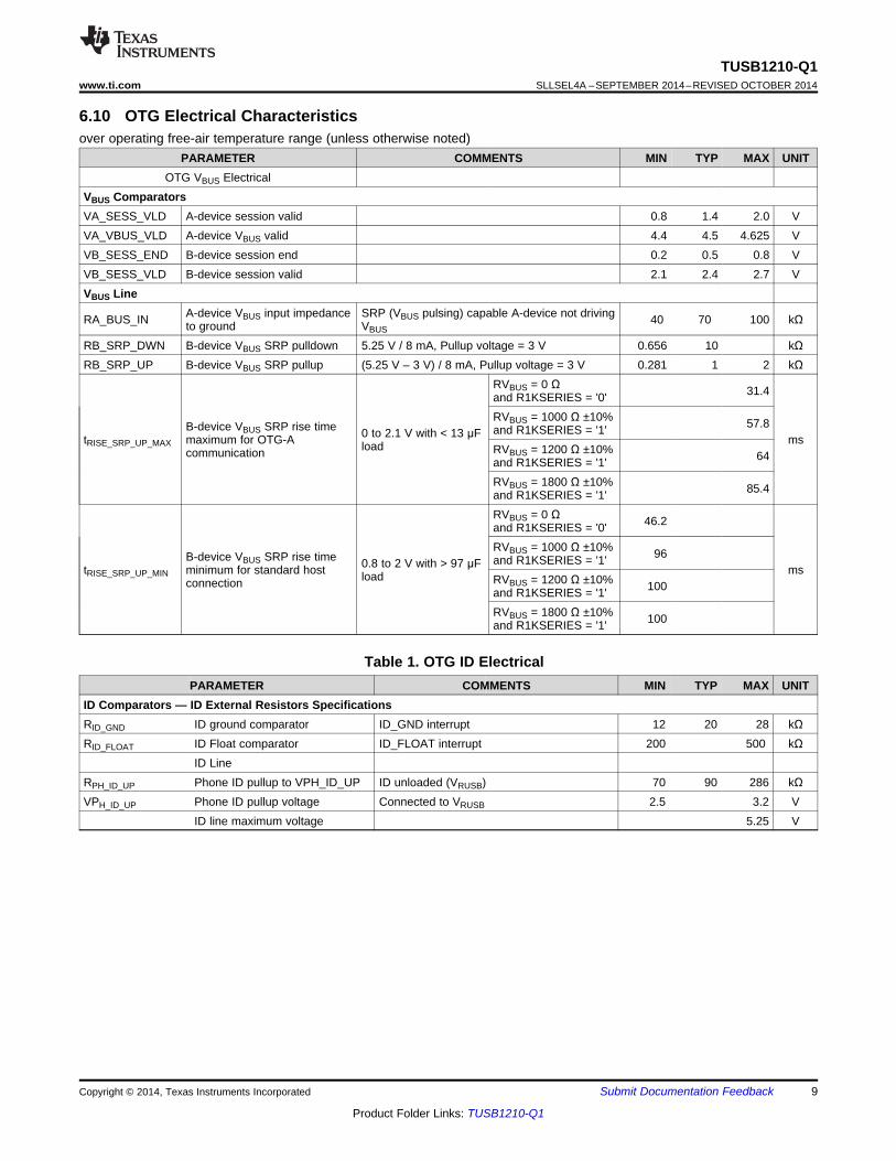
6.10 OTG Electrical Characteristicsover operating free-air temperature range (unless otherwise noted)
PARAMETER COMMENTS MIN TYP MAX UNITOTG VBUS Electrical
VBUS ComparatorsVA_SESS_VLD A-device session valid 0.8 1.4 2.0 VVA_VBUS_VLD A-device VBUS valid 4.4 4.5 4.625 VVB_SESS_END B-device session end 0.2 0.5 0.8 VVB_SESS_VLD B-device session valid 2.1 2.4 2.7 VVBUS Line
A-device VBUS input impedance SRP (VBUS pulsing) capable A-device not drivingRA_BUS_IN 40 70 100 kΩto ground VBUS
RB_SRP_DWN B-device VBUS SRP pulldown 5.25 V / 8 mA, Pullup voltage = 3 V 0.656 10 kΩRB_SRP_UP B-device VBUS SRP pullup (5.25 V – 3 V) / 8 mA, Pullup voltage = 3 V 0.281 1 2 kΩ
RVBUS = 0 Ω 31.4and R1KSERIES = '0'RVBUS = 1000 Ω ±10% 57.8B-device VBUS SRP rise time and R1KSERIES = '1'0 to 2.1 V with < 13 μFtRISE_SRP_UP_MAX maximum for OTG-A msload RVBUS = 1200 Ω ±10%communication 64and R1KSERIES = '1'RVBUS = 1800 Ω ±10% 85.4and R1KSERIES = '1'RVBUS = 0 Ω 46.2and R1KSERIES = '0'RVBUS = 1000 Ω ±10% 96B-device VBUS SRP rise time and R1KSERIES = '1'0.8 to 2 V with > 97 μFtRISE_SRP_UP_MIN minimum for standard host msload RVBUS = 1200 Ω ±10%connection 100and R1KSERIES = '1'RVBUS = 1800 Ω ±10% 100and R1KSERIES = '1'
Table 1. OTG ID ElectricalPARAMETER COMMENTS MIN TYP MAX UNIT
ID Comparators — ID External Resistors SpecificationsRID_GND ID ground comparator ID_GND interrupt 12 20 28 kΩRID_FLOAT ID Float comparator ID_FLOAT interrupt 200 500 kΩ
ID LineRPH_ID_UP Phone ID pullup to VPH_ID_UP ID unloaded (VRUSB) 70 90 286 kΩVPH_ID_UP Phone ID pullup voltage Connected to VRUSB 2.5 3.2 V
ID line maximum voltage 5.25 V
Copyright © 2014, Texas Instruments Incorporated Submit Documentation Feedback 9
Product Folder Links: TUSB1210-Q1

TUSB1210-Q1SLLSEL4A –SEPTEMBER 2014–REVISED OCTOBER 2014 www.ti.com
6.11 Power Characteristicsover operating free-air temperature range (unless otherwise noted)
PARAMETER TEST CONDITIONS MIN TYP MAX UNITVDD33 Internal LDO Regulator CharacteristicsVINVDD33 Input voltage VBAT USB VVDD33 typ + 0.2 3.6 4.5 V
VUSB3V3_VSEL = ‘000 2.4 2.5 2.6VUSB3V3_VSEL = ‘001 2.65 2.75 2.85VUSB3V3_VSEL = ‘010 2.9 3.0 3.1VUSB3V3_VSEL = ‘011 (default) 3.0 3.1 3.2
VVDD33 Output voltage ON mode, VVUSB3V3_VSEL = ‘100 3.1 3.2 3.3VUSB3V3_VSEL = ‘101 3.2 3.3 3.4VUSB3V3_VSEL = ‘110 3.3 3.4 3.5VUSB3V3_VSEL = ‘111 3.4 3.5 3.6Active mode 15
IVDD33 Rated output current VBAT USB mASuspend/reset mode 1
VDD15 Internal LDO Regulator CharacteristicsVIN VDD15 Input voltage On mode, VIN VDD15 = VBAT 2.7 3.6 4.5 VVVDD15 Output voltage VINVDD15 min – VINVDD15 max 1.45 1.56 1.65 VIVDD15 Rated output current On mode 30 mA
6.12 Switching Characteristicsover operating free-air temperature range (unless otherwise noted)
PARAMETER TEST CONDITIONS MIN TYP MAX UNITElectrical Characteristics: Clock Input
Clock input duty cycle 40 60%fCLK Clock nominal frequency 60 MHz
Clock input rise/fall time In % of clock period tCLK ( = 1/fCLK ) 10%Clock input frequency accuracy 250 ppmClock input integrated jitter 600 ps rms
Electrical Characteristics: REFCLKREFCLK input duty cycle 40 60%
When CFG pin is tied to GND 19.2fREFCLK REFCLK nominal frequency MHz
When CFG pin is tied to VDDIO 26In % of clock period tREFCLK ( =REFCLK input rise/fall time 20%1/fREFCLK )
REFCLK input frequency accuracy 250 ppmREFCLK input integrated jitter 600 ps rmsREFCLK HIZ Leakage current 3
µAREFCLK HIZ Leakage current –3
Digital IO Electrical Characteristics: CLOCKtr Rise time Frequency = 60 MHz, Load = 10 pF 1 nstf Fall time Frequency = 30 MHz, Load = 10 pF 1 nsDigital IO Electrical Characteristics: STP, DIR, NXT, DATA0 to DATA7tr Rise time 1 ns
Frequency = 30 MHz, Load = 10 pFtf Fall time 1 ns
10 Submit Documentation Feedback Copyright © 2014, Texas Instruments Incorporated
Product Folder Links: TUSB1210-Q1

VBAT , VDD33
VDDIO, VDD18
IORST
CS
ICACT
VDD15
DIGPOR
CK32K
BGOK
CK32KOK
MNTR_(VDD18,VIO)_OK
MNTR_VDD33_OK
RESETN_PWR
TDELRSTPWR (61us)
TDELMNTRVIOEN (91.5us)
TDELVDD33EN (91.5us)
TMNTR (183.1us)
(input 60M) CLOCK
PLL 480M LOCKED
TPLL (300us)
DIR
TBGAP (2ms)
TPWONVDD15 (100us)
RESETBTDELRESETB (244.1us)
TVBBDET (10us)
TCK32K_PWON (125us)
TMNTR (183.1us)
TDEL_CS_SUPPLYOK (2.84ms) TDEL_RST_DIR (0.54ms)
NO
PW
R
OF
F
HW
RS
T
CO
LD
RS
T
AC
TIV
E
TUSB1210-Q1www.ti.com SLLSEL4A –SEPTEMBER 2014–REVISED OCTOBER 2014
6.13 Timing Requirements
INPUT CLOCK OUTPUT CLOCKPARAMETER UNIT
MIN MAX MIN MAX
ULPI Interface Timing
tSC, tSD Set-up time (control in, 8-bit data in) 3 6 ns
tSC, tHD Hold time (control in, 8-bit data in) 1.5 0 ns
tDC, tDD Output delay (control out, 8-bit data out) 6 9 ns
USB UART Interface Timing
tPH_DP_CON Phone D+ connect time 100 ms
tPH_DISC_DET Phone D+ disconnect time 150 ms
fUART_DFLT Default UART signaling rate (typical rate) 9600 bps
Figure 1. TUSB1210-Q1 Power-Up Timing (ULPI Clock Input Mode)
Table 2. Timers and DebouncePARAMETER COMMENTS MIN TYP MAX UNIT
tDEL_CS_SUPPLYOK Chip-select-to-supplies OK delay 2.84 4.10 ms
RESETB to PHY PLL locked and DIR falling-tDEL_RST_DIR 0.54 0.647 msedge delay
tVBBDET VBAT detection delay 10 µs
tBGAP Bandgap power-on delay 2 ms
tPWONVDD15 VDD15 power-on delay 100 µs
tPWONCK32K 32-KHz RC-OSC power-on delay 125 µs
tDELRSTPWR Power control reset delay 61 µs
tDELMNTRVIOEN Monitor enable delay 91.5 µs
tMNTR Supply monitoring debounce 183.1 µs
tDELVDD33EN VDD33 LDO enable delay 93.75 µs
tDELRESETB RESETB internal delay 244.1 µs
tPLL PLL lock time 300 µs
Copyright © 2014, Texas Instruments Incorporated Submit Documentation Feedback 11
Product Folder Links: TUSB1210-Q1

TUSB1210-Q1SLLSEL4A –SEPTEMBER 2014–REVISED OCTOBER 2014 www.ti.com
6.13.1 Timing Parameter DefinitionsThe timing parameter symbols used in the timing requirement and switching characteristic tables are created inaccordance with JEDEC Standard 100. To shorten the symbols, some pin names and other related terminologieshave been abbreviated as shown in Table 3.
Table 3. Timing Parameter DefinitionsLOWERCASE SUBSCRIPTS
SYMBOL PARAMETERC Cycle time (period)D Delay time
Dis Disable timeEn Enable timeH Hold timeSu Setup time
START Start bitT Transition timeV Valid timeW Pulse duration (width)X Unknown, changing, or don't care levelH HighL LowV ValidIV InvalidAE Active edgeFE First edgeLE Last edgeZ High impedance
6.13.2 Interface Target FrequenciesTable 4 assumes testing over the recommended operating conditions.
Table 4. TUSB1210-Q1 Interface Target FrequenciesIO TARGET FREQUENCYINTERFACE DESIGNATIONINTERFACE 1.5 V
High speed 480 Mbits/sUSB Universal serial bus Full speed 12 Mbits/s
Low speed 1.5 Mbits/s
12 Submit Documentation Feedback Copyright © 2014, Texas Instruments Incorporated
Product Folder Links: TUSB1210-Q1

TUSB1210-Q1www.ti.com SLLSEL4A –SEPTEMBER 2014–REVISED OCTOBER 2014
6.14 Typical Characteristics
Figure 2. High-Speed Eye Diagram Figure 3. Full-Speed Eye Diagram
Copyright © 2014, Texas Instruments Incorporated Submit Documentation Feedback 13
Product Folder Links: TUSB1210-Q1

USB-IP
OTG
1V5
3V3
1V8
POR
VBAT
PLL
PHY
ANA
PHY
DIG
+
ULPI
+
REGS
32KBGAP
& REF
POR
DIG
DIG
TEST
OTG
PWR_ FSM
POR
VIOCTRL
RST_DIG
VDDIO (32)
VBAT (21)
N/C(24)
VDD15 (12)
VDD18 (28)
VDD33 (20)
DP (18)DM (19)
ID (23)
(22)VBUS
( 1) REFCLK
(25) N/C
(17) CPEN
(3:7
,9:1
0,1
3)
DA
TA
(7:0
)(2
)N
XT
(31
)D
IR
(29
)S
TP
(26
)C
LO
CK
(16) N/C
(15) N/C
VDD18 (30)
PKG Substrate
(Ground )
(14) CFG
(11) CS
( 8) N/C
(27) RESETB
TUSB1210-Q1SLLSEL4A –SEPTEMBER 2014–REVISED OCTOBER 2014 www.ti.com
7 Detailed Description
7.1 OverviewThe TUSB1210-Q1 is a USB2.0 transceiver chip, designed to interface with a USB controller via a ULPIinterface. It supports all USB2.0 data rates High-Speed, Full-Speed, and Low-Speed. Compliant to both Host andPeripheral (OTG) modes. It additionally supports a UART mode and legacy ULPI serial modes. TUSB1210-Q1Integrates a 3.3-V LDO, which makes it flexible to work with either battery operated systems or pure 3.3 Vsupplied systems. Also, it has an integrated PLL Supporting 2 Clock Frequencies 19.2 MHz/26 MHz. The ULPIclock pin (60 MHz) supports both input and output clock configurations. TUSB1210-Q1 has low powerconsumption, optimized for portable devices, and complete USB OTG Physical Front-End that supports HostNegotiation Protocol (HNP) and Session Request Protocol (SRP).
TUSB1210-Q1 is optimized to be interfaced through a 12-pin SDR UTMI Low Pin Interface (ULPI), supportingboth input clock and output clock modes, with 1.8 V interface supply voltage.
TUSB1210-Q1 integrates a 3.3 V LDO, which makes it flexible to work with either battery operated systems orpure 3.3 V supplied systems. Both the main supply and the 3.3 V power domain can be supplied through anexternal switched-mode converter for optimized power efficiency.
TUSB1210-Q1 includes a POR circuit to detect supply presence on VBAT and VDDIO pins. TUSB1210-Q1 can bedisabled or configured in low power mode for energy saving.
TUSB1210-Q1 is protected against accidental shorts to 5 V or ground on its exposed interface (DP/DM/ID). It isalso protected against up to 20 V surges on VBUS.
TUSB1210-Q1 integrates a high-performance low-jitter 480 MHz PLL and supports two clock configurations.Depending on the required link configuration, TUSB1210-Q1 supports both ULPI input and output clock mode :input clock mode, in which case a square-wave 60 MHz clock is provided to TUSB1210-Q1 at the ULPI interfaceCLOCK pin; and output clock mode in which case TUSB1210-Q1 can accept a square-wave reference clock atREFCLK of either 19.2 MHz, 26 MHz. Frequency is indicated to TUSB1210-Q1 via the configuration pin CFG.This can be useful if a reference clock is already available in the system.
7.2 Functional Block Diagram
14 Submit Documentation Feedback Copyright © 2014, Texas Instruments Incorporated
Product Folder Links: TUSB1210-Q1

TUSB1210-Q1www.ti.com SLLSEL4A –SEPTEMBER 2014–REVISED OCTOBER 2014
7.3 Feature Description
7.3.1 Processor Subsystem
7.3.1.1 Clock Specifications
7.3.1.1.1 USB PLL Reference Clock
The USB PLL block generates the clocks used to synchronize :• the ULPI interface (60 MHz clock)• the USB interface (depending on the USB data rate, 480 Mbps, 12 Mbps or 1.5 Mbps)
TUSB1210-Q1 requires an external reference clock which is used as an input to the 480 MHz USB PLL block.Depending on the clock configuration, this reference clock can be provided either at REFCLK pin or at CLOCKpin. By default CLK pin is configured as an input.
Two clock configurations are possible:• Input clock configuration (see ULPI Input Clock Configuration)• Output clock configuration (see ULPI Output Clock Configuration)
7.3.1.1.2 ULPI Input Clock Configuration
In this mode REFCLK must be externally tied to GND. CLOCK remains configured as an input.
When the ULPI interface is used in input clock configuration, that is, the 60 MHz ULPI clock is provided toTUSB1210-Q1 on Clock pin, then this is used as the reference clock for the 480 MHz USB PLL block. SeeSwitching Characteristics.
7.3.1.1.3 ULPI Output Clock Configuration
In this mode a reference clock must be externally provided on REFCLK pin When an input clock is detected onREFCLK pin then CLK will automatically change to an output, i.e., 60 MHz ULPI clock is output by TUSB1210-Q1 on CLK pin.
Two reference clock input frequencies are supported. REFCLK input frequency is communicated to TUSB1210-Q1 via a configuration pin, CFG, see fREFCLK in Table 11 for frequency correspondence. TUSB1210-Q1 supportssquare-wave reference clock input only. Reference clock input must be square-wave of amplitude in the range 3V to 3.6 V. See Switching Characteristics.
7.3.1.1.4 Clock 32 kHz
An internal clock generator running at 32 kHz has been implemented to provide a low-speed, low-power clock tothe system See Clock 32 kHz
7.3.1.1.5 Reset
All logic is reset if CS = 0 or VBAT are not present.
All logic (except 32 kHz logic) is reset if VDDIO is not present.
PHY logic is reset when any supplies are not present (VDDIO, VDD15, VDD18, VDD33) or if RESETB pin is low.
TUSB1210-Q1 may be reset manually by toggling the RESETB pin to GND for at lease 200 ns.
If manual reset via RESETB is not required then RESETB pin may be tied to VDDIO permanently.
7.3.1.2 USB TransceiverThe TUSB1210-Q1 device includes a universal serial bus (USB) on-the-go (OTG) transceiver that supports USB480 Mb/s high-speed (HS), 12 Mb/s full-speed (FS), and USB 1.5 Mb/s low-speed (LS) through a 12-pin UTMI+low pin interface (ULPI).
Copyright © 2014, Texas Instruments Incorporated Submit Documentation Feedback 15
Product Folder Links: TUSB1210-Q1

TUSB1210-Q1SLLSEL4A –SEPTEMBER 2014–REVISED OCTOBER 2014 www.ti.com
Feature Description (continued)
NOTELS device mode is not allowed by a USB2.0 HS capable PHY, therefore it is not supportedby TUSB1210-Q1. This is stated in USB2.0 standard Chapter 7, page 119, secondparagraph: “A high-speed capable upstream facing transceiver must not support low-speed signaling mode..” There is also some related commentary in Chapter 7.1.2.3.
7.3.1.2.1 PHY Electrical Characteristics
The PHY is the physical signaling layer of the USB 2.0. It essentially contains all the drivers and receiversrequired for physical data and protocol signaling on the DP and DM lines.
The PHY interfaces to the USB controller through a standard 12-pin digital interface called UTMI+ low pininterface (ULPI).
The transmitters and receivers inside the PHY are classified into two main classes.• The full-speed (FS) and low-speed (LS) transceivers. These are the legacy USB1.x transceivers.• The HS (HS) transceivers
In order to bias the transistors and run the logic, the PHY also contains reference generation circuitry whichconsists of:• A DPLL which does a frequency multiplication to achieve the 480-MHz low-jitter lock necessary for USB and
also the clock required for the switched capacitor resistance block.• A switched capacitor resistance block which is used to replicate an external resistor on chip.
Built-in pullup and pulldown resistors are used as part of the protocol signaling.
Apart from this, the PHY also contains circuitry which protects it from accidental 5-V short on the DP and DMlines.
7.3.1.2.1.1 LS/FS Single-Ended Receivers
In addition to the differential receiver, there is a single-ended receiver (SE–, SE+) for each of the two data linesD+/–. The main purpose of the single-ended receivers is to qualify the D+ and D– signals in the full-speed/low-speed modes of operation. See PHY Electrical Characteristics.
7.3.1.2.1.2 LS/FS Differential Receiver
A differential input receiver (Rx) retrieves the LS/FS differential data signaling. The differential voltage on the lineis converted into digital data by a differential comparator on DP/DM. This data is then sent to a clock and datarecovery circuit which recovers the clock from the data. An additional serial mode exists in which the differentialdata is directly output on the RXRCV pin. See Switching Characteristics.
7.3.1.2.1.3 LS/FS Transmitter
The USB transceiver (Tx) uses a differential output driver to drive the USB data signal D+/– onto the USB cable.The driver's outputs support 3-state operation to achieve bidirectional half-duplex transactions. See SwitchingCharacteristics.
7.3.1.2.1.4 HS Differential Receiver
The HS receiver consists of the following blocks:
A differential input comparator to receive the serial data• A squelch detector to qualify the received data• An oversampler-based clock data recovery scheme followed by a NRZI decoder, bit unstuffing, and serial-to-
parallel converter to generate the ULPI DATAOUTSee Switching Characteristics.
16 Submit Documentation Feedback Copyright © 2014, Texas Instruments Incorporated
Product Folder Links: TUSB1210-Q1
TUSB1210-Q1www.ti.com SLLSEL4A –SEPTEMBER 2014–REVISED OCTOBER 2014
Feature Description (continued)7.3.1.2.1.5 HS Differential Transmitter
The HS transmitter is always operated via the ULPI parallel interface. The parallel data on the interface isserialized, bit stuffed, NRZI encoded, and transmitted as a dc output current on DP or DM depending on thedata. Each line has an effective 22.5-Ω load to ground, which generates the voltage levels for signaling.
A disconnect detector is also part of the HS transmitter. A disconnect on the far end of the cable causes theimpedance seen by the transmitter to double thereby doubling the differential amplitude seen on the DP/DM linesof Switching Characteristics.
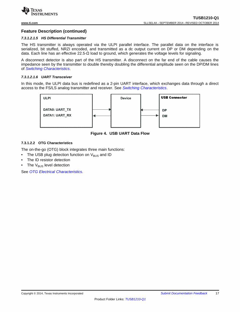
7.3.1.2.1.6 UART Transceiver
In this mode, the ULPI data bus is redefined as a 2-pin UART interface, which exchanges data through a directaccess to the FS/LS analog transmitter and receiver. See Switching Characteristics.
Figure 4. USB UART Data Flow
7.3.1.2.2 OTG Characteristics
The on-the-go (OTG) block integrates three main functions:• The USB plug detection function on VBUS and ID• The ID resistor detection• The VBUS level detection
See OTG Electrical Characteristics.
Copyright © 2014, Texas Instruments Incorporated Submit Documentation Feedback 17
Product Folder Links: TUSB1210-Q1

TUSB1210-Q1SLLSEL4A –SEPTEMBER 2014–REVISED OCTOBER 2014 www.ti.com
7.4 Device Functional Modes
7.4.1 TUSB1210-Q1 Modes vs ULPI Pin StatusTable 5, Table 6, and Table 7 show the status of each of the 12 ULPI pins including input/output direction andwhether output pins are driven to ‘0’ or to ‘1’, or pulled up/pulled down via internal pullup/pulldown resistors.
Note that pullup/pulldown resistors are automatically replaced by driven ‘1’/’0’ levels respectively once internalIORST is released, with the exception of the pullup on STP which is maintained in all modes.
Pin assignment changes in ULPI 3-pin serial mode, ULPI 6-pin serial mode, and UART mode. Unused pins aretied low in these modes as shown below.
Table 5. TUSB1210-Q1 Modes vs ULPI Pin Status:ULPI Synchronous Mode Power-UpULPI SYNCHRONOUS MODE POWER-UP
UNTIL IORST RELEASE PLL OFF PLL ON + STP HIGH PLL ON + STP LOWPIN PIN NAME DIR PU/PD DIR PU/PD DIR PU/PD DIR PU/PDNO.26 CLOCK Hiz PD I PD IO - IO -31 DIR Hiz PU O, (‘1’) - O, (‘0’) - O -2 NXT Hiz PD O, (‘0’) - O, (‘0’) - O -
29 STP Hiz PU I PU I PU I PU3 DATA0 Hiz PD O, (‘0’) - I PD IO -4 DATA1 Hiz PD O, (‘0’) - I PD IO -5 DATA2 Hiz PD O, (‘0’) - I PD IO -6 DATA3 Hiz PD O, (‘0’) - I PD IO -7 DATA4 Hiz PD O, (‘0’) - I PD IO -9 DATA5 Hiz PD O, (‘0’) - I PD IO -
10 DATA6 Hiz PD O, (‘0’) - I PD IO -13 DATA7 Hiz PD O, (‘0’) - I PD IO -
Table 6. TUSB1210-Q1 Modes vs ULPI Pin Status: USB Suspend ModeLINK / EXTERNAL RECOMMENDED SETTING DURINGSUSPEND MODE SUSPEND MODE
PIN NO. PIN NAME DIR PU/PD DIR PU/PD
26 CLOCK I - O -
31 DIR O, (‘1’) - I -
2 NXT O, (‘0’) - I -
29 STP I PU (1) O, (‘0’) -
3 DATA0 O, (LINESTATE0) - I -
4 DATA1 O, (LINESTATE1) - I -
5 DATA2 O, (‘0’) - I -
6 DATA3 O, (INT) - I -
7 DATA4 O, (‘0’) - I -
9 DATA5 O, (‘0’) - I -
10 DATA6 O, (‘0’) - I -
13 DATA7 O, (‘0’) - I -
(1) Can be disabled by software before entering Suspend Mode to reduce current consumption
18 Submit Documentation Feedback Copyright © 2014, Texas Instruments Incorporated
Product Folder Links: TUSB1210-Q1
TUSB1210-Q1www.ti.com SLLSEL4A –SEPTEMBER 2014–REVISED OCTOBER 2014
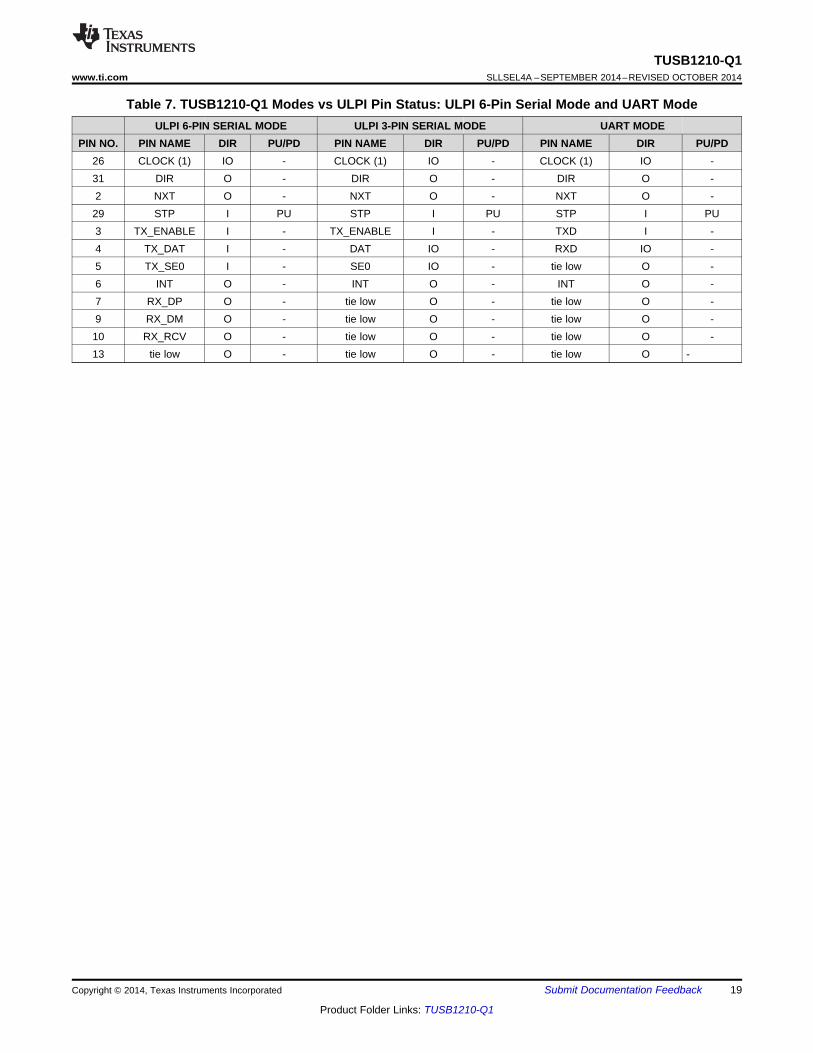
Table 7. TUSB1210-Q1 Modes vs ULPI Pin Status: ULPI 6-Pin Serial Mode and UART ModeULPI 6-PIN SERIAL MODE ULPI 3-PIN SERIAL MODE UART MODE
PIN NO. PIN NAME DIR PU/PD PIN NAME DIR PU/PD PIN NAME DIR PU/PD26 CLOCK (1) IO - CLOCK (1) IO - CLOCK (1) IO -31 DIR O - DIR O - DIR O -2 NXT O - NXT O - NXT O -29 STP I PU STP I PU STP I PU3 TX_ENABLE I - TX_ENABLE I - TXD I -4 TX_DAT I - DAT IO - RXD IO -5 TX_SE0 I - SE0 IO - tie low O -6 INT O - INT O - INT O -7 RX_DP O - tie low O - tie low O -9 RX_DM O - tie low O - tie low O -10 RX_RCV O - tie low O - tie low O -13 tie low O - tie low O - tie low O -
Copyright © 2014, Texas Instruments Incorporated Submit Documentation Feedback 19
Product Folder Links: TUSB1210-Q1

TUSB1210-Q1SLLSEL4A –SEPTEMBER 2014–REVISED OCTOBER 2014 www.ti.com
7.5 Register Map
Table 8. USB Register SummaryREGISTER NAME TYPE REGISTER WIDTH (BITS) PHYSICAL ADDRESSVENDOR_ID_LO R 8 0x00VENDOR_ID_HI R 8 0x01
PRODUCT_ID_LO R 8 0x02PRODUCT_ID_HI R 8 0x03
FUNC_CTRL RW 8 0x04FUNC_CTRL_SET RW 8 0x05FUNC_CTRL_CLR RW 8 0x06
IFC_CTRL RW 8 0x07IFC_CTRL_SET RW 8 0x08IFC_CTRL_CLR RW 8 0x09
OTG_CTRL RW 8 0x0AOTG_CTRL_SET RW 8 0x0BOTG_CTRL_CLR RW 8 0x0C
USB_INT_EN_RISE RW 8 0x0DUSB_INT_EN_RISE_SET RW 8 0x0EUSB_INT_EN_RISE_CLR RW 8 0x0F
USB_INT_EN_FALL RW 8 0x10USB_INT_EN_FALL_SET RW 8 0x11USB_INT_EN_FALL_CLR RW 8 0x12
USB_INT_STS R 8 0x13USB_INT_LATCH R 8 0x14
DEBUG R 8 0x15SCRATCH_REG RW 8 0x16
SCRATCH_REG_SET RW 8 0x17SCRATCH_REG_CLR RW 8 0x18
Reserved R 8 0x19 0x2EACCESS_EXT_REG_SET RW 8 0x2F
Reserved R 8 0x30 0x3CVENDOR_SPECIFIC1 RW 8 0x3D
VENDOR_SPECIFIC1_SET RW 8 0x3EVENDOR_SPECIFIC1_CLR RW 8 0x3F
VENDOR_SPECIFIC2 RW 8 0x80VENDOR_SPECIFIC2_SET RW 8 0x81VENDOR_SPECIFIC2_CLR RW 8 0x82VENDOR_SPECIFIC1_STS R 8 0x83
VENDOR_SPECIFIC1_LATCH R 8 0x84VENDOR_SPECIFIC3 RW 8 0x85
VENDOR_SPECIFIC3_SET RW 8 0x86VENDOR_SPECIFIC3_CLR RW 8 0x87
20 Submit Documentation Feedback Copyright © 2014, Texas Instruments Incorporated
Product Folder Links: TUSB1210-Q1
TUSB1210-Q1www.ti.com SLLSEL4A –SEPTEMBER 2014–REVISED OCTOBER 2014
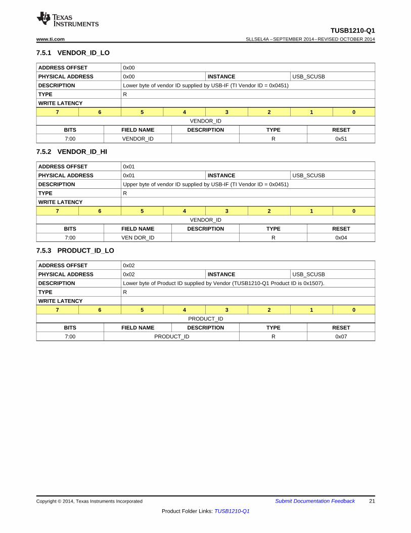
7.5.1 VENDOR_ID_LO
ADDRESS OFFSET 0x00PHYSICAL ADDRESS 0x00 INSTANCE USB_SCUSBDESCRIPTION Lower byte of vendor ID supplied by USB-IF (TI Vendor ID = 0x0451)TYPE RWRITE LATENCY
7 6 5 4 3 2 1 0VENDOR_ID
BITS FIELD NAME DESCRIPTION TYPE RESET7:00 VENDOR_ID R 0x51
7.5.2 VENDOR_ID_HI
ADDRESS OFFSET 0x01PHYSICAL ADDRESS 0x01 INSTANCE USB_SCUSBDESCRIPTION Upper byte of vendor ID supplied by USB-IF (TI Vendor ID = 0x0451)TYPE RWRITE LATENCY
7 6 5 4 3 2 1 0VENDOR_ID
BITS FIELD NAME DESCRIPTION TYPE RESET7:00 VEN DOR_ID R 0x04
7.5.3 PRODUCT_ID_LO
ADDRESS OFFSET 0x02PHYSICAL ADDRESS 0x02 INSTANCE USB_SCUSBDESCRIPTION Lower byte of Product ID supplied by Vendor (TUSB1210-Q1 Product ID is 0x1507).TYPE RWRITE LATENCY
7 6 5 4 3 2 1 0PRODUCT_ID
BITS FIELD NAME DESCRIPTION TYPE RESET7:00 PRODUCT_ID R 0x07
Copyright © 2014, Texas Instruments Incorporated Submit Documentation Feedback 21
Product Folder Links: TUSB1210-Q1

TUSB1210-Q1SLLSEL4A –SEPTEMBER 2014–REVISED OCTOBER 2014 www.ti.com
7.5.4 PRODUCT_ID_HI
ADDRESS OFFSET 0x03PHYSICAL ADDRESS 0x03 INSTANCE USB_SCUSBDESCRIPTION Upper byte of Product ID supplied by Vendor (TUSB1210-Q1 Product ID is 0x1507).TYPE RWRITE LATENCY
7 6 5 4 3 2 1 0PRODUCT_ID
BITS FIELD NAME DESCRIPTION TYPE RESET7:00 PRODUCT_ID R 0x15
7.5.5 FUNC_CTRL
ADDRESS OFFSET 0x04PHYSICAL ADDRESS 0x04 INSTANCE USB_SCUSBDESCRIPTION Controls UTMI function settings of the PHY.TYPE RWWRITE LATENCY
7 6 5 4 3 2 1 0Reserved SUSPENDM RESET OPMODE TERMSELECT XCVRSELECT
BITS FIELD NAME DESCRIPTION TYPE RESET7 Reserved R 06 SUSPENDM Active low PHY suspend. Put PHY into Low Power Mode. In Low Power RW 1
Mode the PHY power down all blocks except the full speed receiver, OTGcomparators, and the ULPI interface pins. The PHY automatically set this bitto '1' when Low Power Mode is exited.
5 RESET Active high transceiver reset. Does not reset the ULPI interface or ULPI RW 0register set.Once set, the PHY asserts the DIR signal and reset the UTMI core. When thereset is completed, the PHY de-asserts DIR and clears this bit. After de-asserting DIR, the PHY re-assert DIR and send an RX command update.Note: This bit is auto-cleared, this explain why it can't be read at '1'.
4:03 OPMODE Select the required bit encoding style during transmit RW 0x00x0: Normal operation0x1: Non-driving0x2: Disable bit-stuff and NRZI encoding0x3: Reserved (No SYNC and EOP generation feature not supported)
2 TERMSELECT Controls the internal 1.5Kohms pull-up resistor and 45ohms HS terminations. RW 0Control over bus resistors changes depending on XcvrSelect, OpMode,DpPulldown and DmPulldown.
1:00 XCVRSELECT Select the required transceiver speed. RW 0x10x0: Enable HS transceiver0x1: Enable FS transceiver0x2: Enable LS transceiver0x3: Enable FS transceiver for LS packets
(FS preamble is automatically pre-pended)
7.5.6 FUNC_CTRL_SET
ADDRESS OFFSET 0x05PHYSICAL ADDRESS 0x05 INSTANCE USB_SCUSB
22 Submit Documentation Feedback Copyright © 2014, Texas Instruments Incorporated
Product Folder Links: TUSB1210-Q1
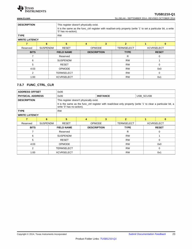
TUSB1210-Q1www.ti.com SLLSEL4A –SEPTEMBER 2014–REVISED OCTOBER 2014
DESCRIPTION This register doesn't physically exist.It is the same as the func_ctrl register with read/set-only property (write '1' to set a particular bit, a write'0' has no-action).
TYPE RWWRITE LATENCY
7 6 5 4 3 2 1 0Reserved SUSPENDM RESET OPMODE TERMSELECT XCVRSELECT
BITS FIELD NAME DESCRIPTION TYPE RESET7 Reserved R 06 SUSPENDM RW 15 RESET RW 0
4:03 OPMODE RW 0x02 TERMSELECT RW 0
1:00 XCVRSELECT RW 0x1
7.5.7 FUNC_CTRL_CLR
ADDRESS OFFSET 0x06PHYSICAL ADDRESS 0x06 INSTANCE USB_SCUSBDESCRIPTION This register doesn't physically exist.
It is the same as the func_ctrl register with read/clear-only property (write '1' to clear a particular bit, awrite '0' has no-action).
TYPE RWWRITE LATENCY
7 6 5 4 3 2 1 0Reserved SUSPENDM RESET OPMODE TERMSELECT XCVRSELECT
BITS FIELD NAME DESCRIPTION TYPE RESET7 Reserved R 06 SUSPENDM RW 15 RESET RW 0
4:03 OPMODE RW 0x02 TERMSELECT RW 0
1:00 XCVRSELECT RW 0x1
Copyright © 2014, Texas Instruments Incorporated Submit Documentation Feedback 23
Product Folder Links: TUSB1210-Q1
TUSB1210-Q1SLLSEL4A –SEPTEMBER 2014–REVISED OCTOBER 2014 www.ti.com
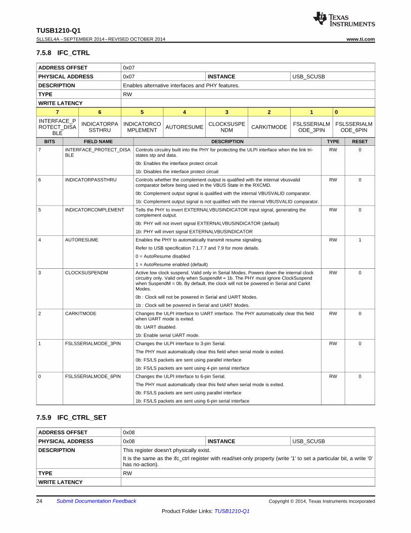
7.5.8 IFC_CTRL
ADDRESS OFFSET 0x07PHYSICAL ADDRESS 0x07 INSTANCE USB_SCUSBDESCRIPTION Enables alternative interfaces and PHY features.TYPE RWWRITE LATENCY
7 6 5 4 3 2 1 0INTERFACE_P INDICATORPA INDICATORCO CLOCKSUSPE FSLSSERIALM FSLSSERIALMROTECT_DISA AUTORESUME CARKITMODESSTHRU MPLEMENT NDM ODE_3PIN ODE_6PINBLE
BITS FIELD NAME DESCRIPTION TYPE RESET
7 INTERFACE_PROTECT_DISA Controls circuitry built into the PHY for protecting the ULPI interface when the link tri- RW 0BLE states stp and data.
0b: Enables the interface protect circuit
1b: Disables the interface protect circuit
6 INDICATORPASSTHRU Controls whether the complement output is qualified with the internal vbusvalid RW 0comparator before being used in the VBUS State in the RXCMD.
0b: Complement output signal is qualified with the internal VBUSVALID comparator.
1b: Complement output signal is not qualified with the internal VBUSVALID comparator.
5 INDICATORCOMPLEMENT Tells the PHY to invert EXTERNALVBUSINDICATOR input signal, generating the RW 0complement output.
0b: PHY will not invert signal EXTERNALVBUSINDICATOR (default)
1b: PHY will invert signal EXTERNALVBUSINDICATOR
4 AUTORESUME Enables the PHY to automatically transmit resume signaling. RW 1
Refer to USB specification 7.1.7.7 and 7.9 for more details.
0 = AutoResume disabled
1 = AutoResume enabled (default)
3 CLOCKSUSPENDM Active low clock suspend. Valid only in Serial Modes. Powers down the internal clock RW 0circuitry only. Valid only when SuspendM = 1b. The PHY must ignore ClockSuspendwhen SuspendM = 0b. By default, the clock will not be powered in Serial and CarkitModes.
0b : Clock will not be powered in Serial and UART Modes.
1b : Clock will be powered in Serial and UART Modes.
2 CARKITMODE Changes the ULPI interface to UART interface. The PHY automatically clear this field RW 0when UART mode is exited.
0b: UART disabled.
1b: Enable serial UART mode.
1 FSLSSERIALMODE_3PIN Changes the ULPI interface to 3-pin Serial. RW 0
The PHY must automatically clear this field when serial mode is exited.
0b: FS/LS packets are sent using parallel interface
1b: FS/LS packets are sent using 4-pin serial interface
0 FSLSSERIALMODE_6PIN Changes the ULPI interface to 6-pin Serial. RW 0
The PHY must automatically clear this field when serial mode is exited.
0b: FS/LS packets are sent using parallel interface
1b: FS/LS packets are sent using 6-pin serial interface
7.5.9 IFC_CTRL_SET
ADDRESS OFFSET 0x08PHYSICAL ADDRESS 0x08 INSTANCE USB_SCUSBDESCRIPTION This register doesn't physically exist.
It is the same as the ifc_ctrl register with read/set-only property (write '1' to set a particular bit, a write '0'has no-action).
TYPE RWWRITE LATENCY
24 Submit Documentation Feedback Copyright © 2014, Texas Instruments Incorporated
Product Folder Links: TUSB1210-Q1

TUSB1210-Q1www.ti.com SLLSEL4A –SEPTEMBER 2014–REVISED OCTOBER 2014
7 6 5 4 3 2 1 0INTERFACE_P INDICATORPA INDICATORCO AUTORESUME CLOCKSUSPE CARKITMODE FSLSSERIALM FSLSSERIALMROTECT_DISA SSTHRU MPLEMENT NDM ODE_3PIN ODE_6PIN
BLEBITS FIELD NAME DESCRIPTION TYPE RESET
7 INTERFACE_PROTECT_DISABLE RW 06 INDICATORPASSTHRU RW 05 INDICATORCOMPLEMENT RW 04 AUTORESUME RW 13 CLOCKSUSPENDM RW 02 CARKITMODE RW 01 FSLSSERIALMODE_3PIN RW 00 FSLSSERIALMODE_6PIN R 0
Copyright © 2014, Texas Instruments Incorporated Submit Documentation Feedback 25
Product Folder Links: TUSB1210-Q1

TUSB1210-Q1SLLSEL4A –SEPTEMBER 2014–REVISED OCTOBER 2014 www.ti.com
7.5.10 IFC_CTRL_CLR
ADDRESS OFFSET 0x09PHYSICAL ADDRESS 0x09 INSTANCE USB_SCUSBDESCRIPTION This register doesn't physically exist.
It is the same as the ifc_ctrl register with read/clear-only property (write '1' to clear a particular bit, awrite '0' has no-action).
TYPE RWWRITE LATENCY
7 6 5 4 3 2 1 0INTERFACE_P IN INDICATORCO AUTORESUME CLOCKSUSPE CARKITMODE FSLSSERIALM FSLSSERIALMROTECT_DISA DICATORPAS MPLEMENT NDM ODE_3PIN ODE_6PIN
BLE STHRUBITS FIELD NAME DESCRIPTION TYPE RESET
7 INTERFACE_PROTECT_DISABLE RW 06 INDICATORPASSTHRU RW 05 INDICATORCOMPLEMENT RW 04 AUTORESUME RW 13 CLOCKSUSPENDM RW 02 CARKITMODE RW 01 FSLSSERIALMODE_3PIN RW 00 FSLSSERIALMODE_6PIN R 0
26 Submit Documentation Feedback Copyright © 2014, Texas Instruments Incorporated
Product Folder Links: TUSB1210-Q1

TUSB1210-Q1www.ti.com SLLSEL4A –SEPTEMBER 2014–REVISED OCTOBER 2014
7.5.11 OTG_CTRL
ADDRESS OFFSET 0x0APHYSICAL ADDRESS 0x0A INSTANCE USB_SCUSBDESCRIPTION Controls UTMI+ OTG functions of the PHY.TYPE RWWRITE LATENCY
7 6 5 4 3 2 1 0USEEXTERNA DRVVBUSEXT DRVVBUS CHRGVBUS DISCHRGVBU DMPULLDOW DPPULLDOWN IDPULLUPLVBUSINDICA ERNAL S N
TORBITS FIELD NAME DESCRIPTION TYPE RESET
7 USEEXTERNALVBUSINDICATO Tells the PHY to use an external VBUS over-current indicator. RW 0R
0b: Use the internal OTG comparator (VA_VBUS_VLD) or internal VBUS validindicator (default)
1b: Use external VBUS valid indicator signal.
6 DRVVBUSEXTERNAL Selects between the internal and the external 5 V VBUS supply. RW 0
0b: Pin17 (CPEN) is disabled (output GND level). TUSB1210-Q1 does notsupport internal VBUS supply.
1b: Pin17 (CPEN) is set to ‘1’ (output VDD33 voltage level) if DRVVBUS bit is‘1’, else Pin17 (CPEN) is disabled (output GND level) if DRVVBUS bit is ‘0’
5 DRVVBUS VBUS output control bit RW 0
0b : do not drive VBUS
1b : drive 5V on VBUS
Note: Both DRVVBUS and DRVVBUSEXTERNAL bits must be set to 1 in orderto to set Pin17 (CPEN). CPEN pin can be used to enable an external VBUSsupply
4 CHRGVBUS Charge VBUS through a resistor. Used for VBUS pulsing SRP. The Link must RW 0first check that VBUS has been discharged (see DischrgVbus register bit), andthat both D+ and D- data lines have been low (SE0) for 2ms.
0b : do not charge VBUS
1b : charge VBUS
3 DISCHRGVBUS Discharge VBUS through a resistor. If the Link sets this bit to 1, it waits for an RW 0RX CMD indicating SessEnd has transitioned from 0 to 1, and then resets thisbit to 0 to stop the discharge.
0b : do not discharge VBUS
1b : discharge VBUS
2 DMPULLDOWN Enables the 15k Ohm pull-down resistor on D-. RW 1
0b : Pull-down resistor not connected to D-.
1b : Pull-down resistor connected to D-.
1 DPPULLDOWN Enables the 15k Ohm pull-down resistor on D+. RW 1
0b : Pull-down resistor not connected to D+.
1b : Pull-down resistor connected to D+.
0 IDPULLUP Connects a pull-up to the ID line and enables sampling of the signal level. RW 0
0b : Disable sampling of ID line.
1b : Enable sampling of ID line.
7.5.12 OTG_CTRL_SET
ADDRESS OFFSET 0x0BPHYSICAL ADDRESS 0x0B INSTANCE USB_SCUSBDESCRIPTION This register doesn't physically exist.
It is the same as the otg_ctrl register with read/set-only property (write '1' to set a particular bit, a write'0' has no-action).
TYPE RWWRITE LATENCY
Copyright © 2014, Texas Instruments Incorporated Submit Documentation Feedback 27
Product Folder Links: TUSB1210-Q1

TUSB1210-Q1SLLSEL4A –SEPTEMBER 2014–REVISED OCTOBER 2014 www.ti.com
7 6 5 4 3 2 1 0USEEXTERNA DRVVBUSEXT DISCHRGVBU DMPULLDOWLVBUSINDICA DRVVBUS CHRGVBUS DPPULLDOWN IDPULLUPERNAL S NTOR
BITS FIELD NAME DESCRIPTION TYPE RESET7 USEEXTERNALVBUSINDICATOR RW 06 DRVVBUSEXTERNAL RW 05 DRVVBUS RW 04 CHRGVBUS RW 03 DISCHRGVBUS RW 02 DMPULLDOWN RW 11 DPPULLDOWN RW 10 IDPULLUP RW 0
28 Submit Documentation Feedback Copyright © 2014, Texas Instruments Incorporated
Product Folder Links: TUSB1210-Q1
TUSB1210-Q1www.ti.com SLLSEL4A –SEPTEMBER 2014–REVISED OCTOBER 2014
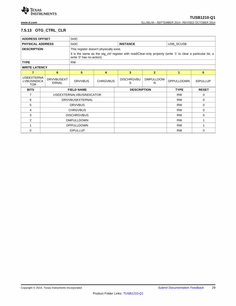
7.5.13 OTG_CTRL_CLR
ADDRESS OFFSET 0x0CPHYSICAL ADDRESS 0x0C INSTANCE USB_SCUSBDESCRIPTION This register doesn't physically exist.
It is the same as the otg_ctrl register with read/Clear-only property (write '1' to clear a particular bit, awrite '0' has no-action).
TYPE RWWRITE LATENCY
7 6 5 4 3 2 1 0USEEXTERNA DRVVBUSEXT DISCHRGVBU DMPULLDOWLVBUSINDICA DRVVBUS CHRGVBUS DPPULLDOWN IDPULLUPERNAL S NTOR
BITS FIELD NAME DESCRIPTION TYPE RESET7 USEEXTERNALVBUSINDICATOR RW 06 DRVVBUSEXTERNAL RW 05 DRVVBUS RW 04 CHRGVBUS RW 03 DISCHRGVBUS RW 02 DMPULLDOWN RW 11 DPPULLDOWN RW 10 IDPULLUP RW 0
Copyright © 2014, Texas Instruments Incorporated Submit Documentation Feedback 29
Product Folder Links: TUSB1210-Q1

TUSB1210-Q1SLLSEL4A –SEPTEMBER 2014–REVISED OCTOBER 2014 www.ti.com
7.5.14 USB_INT_EN_RISE
ADDRESS OFFSET 0x0DPHYSICAL ADDRESS 0x0D INSTANCE USB_SCUSBDESCRIPTION If set, the bits in this register cause an interrupt event notification to be generated when the
corresponding PHY signal changes from low to high. By default, all transitions are enabled.TYPE RWWRITE LATENCY
7 6 5 4 3 2 1 0SESSEND_RIS SESSVALID_RI VBUSVALID_R HOSTDISCONReserved Reserved Reserved IDGND_RISE E SE ISE NECT_RISE
BITS FIELD NAME DESCRIPTION TYPE RESET7 Reserved R 06 Reserved R 05 Reserved R 04 IDGND_RISE Generate an interrupt event notification when IdGnd changes from RW 1
low to high.Event is automatically masked if IdPullup bit is clear to 0 and for
50ms after IdPullup is set to 1.3 SESSEND_RISE Generate an interrupt event notification when SessEnd changes RW 1
from low to high.2 SESSVALID_RISE Generate an interrupt event notification when SessValid changes RW 1
from low to high. SessValid is the same as UTMI+ AValid.1 VBUSVALID_RISE Generate an interrupt event notification when VbusValid changes RW 1
from low to high.0 HOSTDISCONNECT_RISE Generate an interrupt event notification when Hostdisconnect RW 1
changes from low to high. Applicable only in host mode(DpPulldown and DmPulldown both set to 1b).
30 Submit Documentation Feedback Copyright © 2014, Texas Instruments Incorporated
Product Folder Links: TUSB1210-Q1

TUSB1210-Q1www.ti.com SLLSEL4A –SEPTEMBER 2014–REVISED OCTOBER 2014
7.5.15 USB_INT_EN_RISE_SET
ADDRESS OFFSET 0x0EPHYSICAL ADDRESS 0x0E INSTANCE USB_SCUSBDESCRIPTION This register doesn't physically exist.
It is the same as the usb_int_en_rise register with read/set-only property (write '1' to set a particular bit,a write '0' has no-action).
TYPE RWWRITE LATENCY
7 6 5 4 3 2 1 0SESSEND_RIS SESSVALID_RI VBUSVALID_R HOSTDISCONReserved Reserved Reserved IDGND_RISE E SE ISE NECT_RISE
BITS FIELD NAME DESCRIPTION TYPE RESET7 Reserved R 06 Reserved R 05 Reserved R 04 IDGND_RISE RW 13 SESSEND_RISE RW 12 SESSVALID_RISE RW 11 VBUSVALID_RISE RW 10 HOSTDISCONNECT_RIS RW 1
E
Copyright © 2014, Texas Instruments Incorporated Submit Documentation Feedback 31
Product Folder Links: TUSB1210-Q1

TUSB1210-Q1SLLSEL4A –SEPTEMBER 2014–REVISED OCTOBER 2014 www.ti.com
7.5.16 USB_INT_EN_RISE_CLR
ADDRESS OFFSET 0x0FPHYSICAL ADDRESS 0x0F INSTANCE USB_SCUSBDESCRIPTION This register doesn't physically exist.
It is the same as the usb_int_en_rise register with read/clear-only property (write '1' to clear a particularbit, a write '0' has no-action).
TYPE RWWRITE LATENCY
7 6 5 4 3 2 1 0SESSEN SESSVALID_RI VBUSVALID_R HOSTDISCONReserved Reserved Reserved IDGND_RISE D_RISE SE ISE NECT_RISE
BITS FIELD NAME DESCRIPTION TYPE RESET7 Reserved R 06 Reserved R 05 Reserved R 04 IDGND_RISE RW 13 SESSEND_RISE RW 12 SESSVALID_RISE RW 11 VBUSVALID_RISE RW 10 HOSTDISCONNECT_RISE RW 1
32 Submit Documentation Feedback Copyright © 2014, Texas Instruments Incorporated
Product Folder Links: TUSB1210-Q1

TUSB1210-Q1www.ti.com SLLSEL4A –SEPTEMBER 2014–REVISED OCTOBER 2014
7.5.17 USB_INT_EN_FALL
ADDRESS OFFSET 0x10PHYSICAL ADDRESS 0x10 INSTANCE USB_SCUSBDESCRIPTION If set, the bits in this register cause an interrupt event notification to be generated when the
corresponding PHY signal changes from low to high. By default, all transitions are enabled.TYPE RWWRITE LATENCY
7 6 5 4 3 2 1 0SESSEND_FA SESSVALID_F VBUSVALID_F HOSTDISCONReserved Reserved Reserved IDGND_FALL LL ALL ALL NECT_FALL
BITS FIELD NAME DESCRIPTION TYPE RESET7 Reserved R 06 Reserved R 05 Reserved R 04 IDGND_FALL Generate an interrupt event notification when IdGnd changes RW 1
from high to low.Event is automatically masked if IdPullup bit is clear to 0 and for50ms after IdPullup is set to 1.
3 SESSEND_FALL Generate an interrupt event notification when SessEnd changes RW 1from high to low.
2 SESSVALID_FALL Generate an interrupt event notification when SessValid changes RW 1from high to low. SessValid is the same as UTMI+ AValid.
1 VBUSVALID_FALL Generate an interrupt event notification when VbusValid changes RW 1from high to low.
0 HOSTDISCONNECT_FALL Generate an interrupt event notification when Hostdisconnect RW 1changes from high to low. Applicable only in host mode(DpPulldown and DmPulldown both set to 1b).
Copyright © 2014, Texas Instruments Incorporated Submit Documentation Feedback 33
Product Folder Links: TUSB1210-Q1

TUSB1210-Q1SLLSEL4A –SEPTEMBER 2014–REVISED OCTOBER 2014 www.ti.com
7.5.18 USB_INT_EN_FALL_SET
ADDRESS OFFSET 0x11PHYSICAL ADDRESS 0x11 INSTANCE USB_SCUSBDESCRIPTION This register doesn't physically exist.
It is the same as the usb_int_en_fall register with read/set-only property (write '1' to set a particular bit, awrite '0' has no-action)
TYPE RWWRITE LATENCY
7 6 5 4 3 2 1 0SESSEND_FA SESSVALID_F VBUSVALID_F HOSTDISCONReserved Reserved Reserved IDGND_FALL LL ALL ALL NECT_FALL
BITS FIELD NAME DESCRIPTION TYPE RESET7 Reserved R 06 Reserved R 05 Reserved R 04 IDGND_FALL RW 13 SESSEND_FALL RW 12 SESSVALID_FALL RW 11 VBUSVALID_FALL RW 10 HOSTDISCONNECT_FALL RW 1
34 Submit Documentation Feedback Copyright © 2014, Texas Instruments Incorporated
Product Folder Links: TUSB1210-Q1

TUSB1210-Q1www.ti.com SLLSEL4A –SEPTEMBER 2014–REVISED OCTOBER 2014
7.5.19 USB_INT_EN_FALL_CLR
ADDRESS OFFSET 0x12PHYSICAL ADDRESS 0x12 INSTANCE USB_SCUSBDESCRIPTION This register doesn't physically exist.
It is the same as the usb_int_en_fall register with read/clear-only property (write '1' to clear a particularbit, a write '0' has no-action).
TYPE RWWRITE LATENCY
7 6 5 4 3 2 1 0SESSEND_FA SESSVALID_F VBUSVALID_F HOSTDISCONReserved Reserved Reserved IDGND_FALL LL ALL ALL NECT_FALL
BITS FIELD NAME DESCRIPTION TYPE RESET7 Reserved R 06 Reserved R 05 Reserved R 04 IDGND_FALL RW 13 SESSEN D_FALL RW 12 SESSVALID_FALL RW 11 VBUSVALID_FALL RW 10 HOSTDISCONNECT_FALL RW 1
Copyright © 2014, Texas Instruments Incorporated Submit Documentation Feedback 35
Product Folder Links: TUSB1210-Q1

TUSB1210-Q1SLLSEL4A –SEPTEMBER 2014–REVISED OCTOBER 2014 www.ti.com
7.5.20 USB_INT_STS
ADDRESS OFFSET 0x13PHYSICAL ADDRESS 0x13 INSTANCE USB_SCUSBDESCRIPTION Indicates the current value of the interrupt source signal.TYPE RWRITE LATENCY
7 6 5 4 3 2 1 0Reserved Reserved Reserved IDGND SESSEND SESSVALID VBUSVALID HOSTDISCON
NECTBITS FIELD NAME DESCRIPTION TYPE RESET
7 Reserved R 06 Reserved R 05 Reserved R 04 IDGND Current value of UTMI+ IdGnd output. R 0
This bit is not updated if IdPullup bit is reset to 0 and for 50 ms after IdPullup is set to1.
3 SESSEND Current value of UTMI+ SessEnd output. R 02 SESSVALID Current value of UTMI+ SessValid output. SessValid is the same as UTMI+ AValid. R 01 VBUSVALID Current value of UTMI+ VbusValid output. R 00 HOSTDISCONNECT Current value of UTMI+ Hostdisconnect output. R 0
Applicable only in host mode.Automatically reset to 0 when Low Power Mode is entered.NOTE: Reset value is '0' when host is connected.Reset value is '1' when host is disconnected.
36 Submit Documentation Feedback Copyright © 2014, Texas Instruments Incorporated
Product Folder Links: TUSB1210-Q1
TUSB1210-Q1www.ti.com SLLSEL4A –SEPTEMBER 2014–REVISED OCTOBER 2014
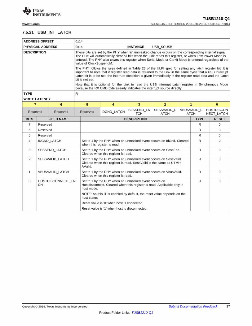
7.5.21 USB_INT_LATCH
ADDRESS OFFSET 0x14PHYSICAL ADDRESS 0x14 INSTANCE USB_SCUSBDESCRIPTION These bits are set by the PHY when an unmasked change occurs on the corresponding internal signal.
The PHY will automatically clear all bits when the Link reads this register, or when Low Power Mode isentered. The PHY also clears this register when Serial Mode or Carkit Mode is entered regardless of thevalue of ClockSuspendM.The PHY follows the rules defined in Table 26 of the ULPI spec for setting any latch register bit. It isimportant to note that if register read data is returned to the Link in the same cycle that a USB InterruptLatch bit is to be set, the interrupt condition is given immediately in the register read data and the Latchbit is not set.Note that it is optional for the Link to read the USB Interrupt Latch register in Synchronous Modebecause the RX CMD byte already indicates the interrupt source directly
TYPE RWRITE LATENCY
7 6 5 4 3 2 1 0SESSEND_LA SESSVALID_L VBUSVALID_L HOSTDISCONReserved Reserved Reserved IDGND_LATCH TCH ATCH ATCH NECT_LATCH
BITS FIELD NAME DESCRIPTION TYPE RESET7 Reserved R 06 Reserved R 05 Reserved R 04 IDGND_LATCH Set to 1 by the PHY when an unmasked event occurs on IdGnd. Cleared R 0
when this register is read.3 SESSEND_LATCH Set to 1 by the PHY when an unmasked event occurs on SessEnd. R 0
Cleared when this register is read.2 SESSVALID_LATCH Set to 1 by the PHY when an unmasked event occurs on SessValid. R 0
Cleared when this register is read. SessValid is the same as UTMI+AValid.
1 VBUSVALID_LATCH Set to 1 by the PHY when an unmasked event occurs on VbusValid. R 0Cleared when this register is read.
0 HOSTDISCONNECT_LAT Set to 1 by the PHY when an unmasked event occurs on R 0CH Hostdisconnect. Cleared when this register is read. Applicable only in
host mode.NOTE: As this IT is enabled by default, the reset value depends on thehost statusReset value is '0' when host is connected.Reset value is '1' when host is disconnected.
Copyright © 2014, Texas Instruments Incorporated Submit Documentation Feedback 37
Product Folder Links: TUSB1210-Q1
TUSB1210-Q1SLLSEL4A –SEPTEMBER 2014–REVISED OCTOBER 2014 www.ti.com
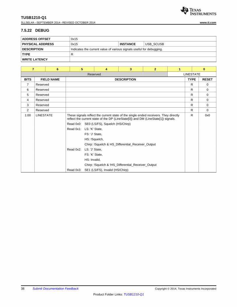
7.5.22 DEBUG
ADDRESS OFFSET 0x15PHYSICAL ADDRESS 0x15 INSTANCE USB_SCUSBDESCRIPTION Indicates the current value of various signals useful for debugging.TYPE RWRITE LATENCY
7 6 5 4 3 2 1 0Reserved LINESTATE
BITS FIELD NAME DESCRIPTION TYPE RESET7 Reserved R 06 Reserved R 05 Reserved R 04 Reserved R 03 Reserved R 02 Reserved R 0
1:00 LINESTATE These signals reflect the current state of the single ended receivers. They directly R 0x0reflect the current state of the DP (LineState[0]) and DM (LineState[1]) signals.Read 0x0: SE0 (LS/FS), Squelch (HS/Chirp)Read 0x1: LS: 'K' State,
FS: 'J' State,HS: !Squelch,Chirp: !Squelch & HS_Differential_Receiver_Output
Read 0x2: LS: 'J' State,FS: 'K' State,HS: Invalid,Chirp: !Squelch & !HS_Differential_Receiver_Output
Read 0x3: SE1 (LS/FS), Invalid (HS/Chirp)
38 Submit Documentation Feedback Copyright © 2014, Texas Instruments Incorporated
Product Folder Links: TUSB1210-Q1

TUSB1210-Q1www.ti.com SLLSEL4A –SEPTEMBER 2014–REVISED OCTOBER 2014
7.5.23 SCRATCH_REG
ADDRESS OFFSET 0x16PHYSICAL ADDRESS 0x16 INSTANCE USB_SCUSBDESCRIPTION Empty register byte for testing purposes. Software can read, write, set, and clear this register and the
PHY functionality will not be affected.TYPE RWWRITE LATENCY
7 6 5 4 3 2 1 0SCRATCH
BITS FIELD NAME DESCRIPTION TYPE RESET7:00 SCRATCH Scratch data. RW 0x00
7.5.24 SCRATCH_REG_SET
ADDRESS OFFSET 0x17PHYSICAL ADDRESS 0x17 INSTANCE USB_SCUSBDESCRIPTION This register doesn't physically exist.
It is the same as the scratch_reg register with read/set-only property (write '1' to set a particular bit, awrite '0' has no-action).
TYPE RWWRITE LATENCY
7 6 5 4 3 2 1 0SCRATCH
BITS FIELD NAME DESCRIPTION TYPE RESET7:00 SCRATCH RW 0x00
7.5.25 SCRATCH_REG_CLR
ADDRESS OFFSET 0x18PHYSICAL ADDRESS 0x18 INSTANCE USB_SCUSBDESCRIPTION This register doesn't physically exist.
It is the same as the scratch_reg with read/clear-only property (write '1' to clear a particular bit, a write'0' has no-action).
TYPE RWWRITE LATENCY
7 6 5 4 3 2 1 0SCRATCH
BITS FIELD NAME DESCRIPTION TYPE RESET7:00 SCRATCH RW 0x00
Copyright © 2014, Texas Instruments Incorporated Submit Documentation Feedback 39
Product Folder Links: TUSB1210-Q1
TUSB1210-Q1SLLSEL4A –SEPTEMBER 2014–REVISED OCTOBER 2014 www.ti.com
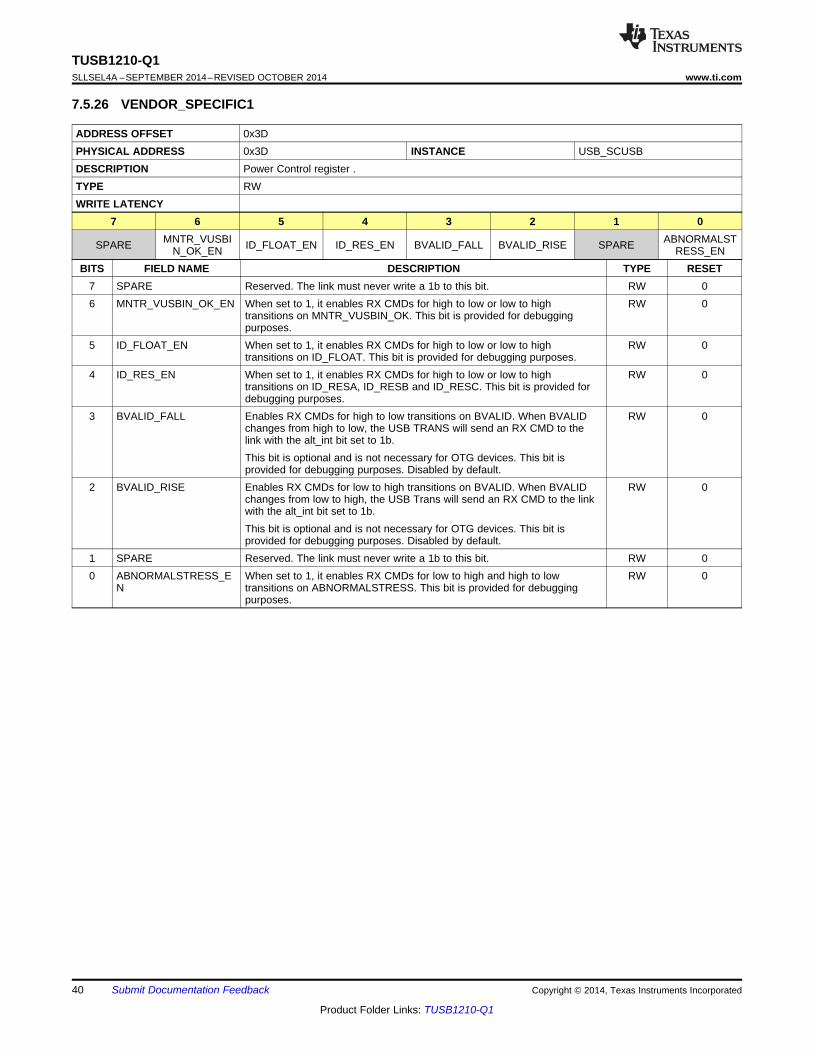
7.5.26 VENDOR_SPECIFIC1
ADDRESS OFFSET 0x3DPHYSICAL ADDRESS 0x3D INSTANCE USB_SCUSBDESCRIPTION Power Control register .TYPE RWWRITE LATENCY
7 6 5 4 3 2 1 0MNTR_VUSBI ABNORMALSTSPARE ID_FLOAT_EN ID_RES_EN BVALID_FALL BVALID_RISE SPAREN_OK_EN RESS_EN
BITS FIELD NAME DESCRIPTION TYPE RESET7 SPARE Reserved. The link must never write a 1b to this bit. RW 06 MNTR_VUSBIN_OK_EN When set to 1, it enables RX CMDs for high to low or low to high RW 0
transitions on MNTR_VUSBIN_OK. This bit is provided for debuggingpurposes.
5 ID_FLOAT_EN When set to 1, it enables RX CMDs for high to low or low to high RW 0transitions on ID_FLOAT. This bit is provided for debugging purposes.
4 ID_RES_EN When set to 1, it enables RX CMDs for high to low or low to high RW 0transitions on ID_RESA, ID_RESB and ID_RESC. This bit is provided fordebugging purposes.
3 BVALID_FALL Enables RX CMDs for high to low transitions on BVALID. When BVALID RW 0changes from high to low, the USB TRANS will send an RX CMD to thelink with the alt_int bit set to 1b.This bit is optional and is not necessary for OTG devices. This bit isprovided for debugging purposes. Disabled by default.
2 BVALID_RISE Enables RX CMDs for low to high transitions on BVALID. When BVALID RW 0changes from low to high, the USB Trans will send an RX CMD to the linkwith the alt_int bit set to 1b.This bit is optional and is not necessary for OTG devices. This bit isprovided for debugging purposes. Disabled by default.
1 SPARE Reserved. The link must never write a 1b to this bit. RW 00 ABNORMALSTRESS_E When set to 1, it enables RX CMDs for low to high and high to low RW 0
N transitions on ABNORMALSTRESS. This bit is provided for debuggingpurposes.
40 Submit Documentation Feedback Copyright © 2014, Texas Instruments Incorporated
Product Folder Links: TUSB1210-Q1

TUSB1210-Q1www.ti.com SLLSEL4A –SEPTEMBER 2014–REVISED OCTOBER 2014
7.5.27 VENDOR_SPECIFIC1_SET
ADDRESS OFFSET 0x3EPHYSICAL ADDRESS 0x3E INSTANCE USB_SCUSBDESCRIPTION This register doesn't physically exist.
It is the same as the func_ctrl register with read/set-only property (write '1' to set a particular bit, a write'0' has no-action).
TYPE RWWRITE LATEN CY
7 6 5 4 3 2 1 0MNTR_VUSBI ABNORMALSTSPARE ID_FLOAT_EN ID_RES_EN BVALID_FALL BVALID_RISE SPAREN_OK_EN RESS_EN
BITS FIELD NAME DESCRIPTION TYPE RESET7 SPARE RW 06 MNTR_VUSBIN_OK_EN RW 05 ID_FLOAT_EN RW 04 ID_RES_EN RW 03 BVALID_FALL RW 02 BVALID_RISE RW 01 SPARE RW 00 ABNORMALSTRESS_EN RW 0
Copyright © 2014, Texas Instruments Incorporated Submit Documentation Feedback 41
Product Folder Links: TUSB1210-Q1

TUSB1210-Q1SLLSEL4A –SEPTEMBER 2014–REVISED OCTOBER 2014 www.ti.com
7.5.28 VENDOR_SPECIFIC1_CLR
ADDRESS OFFSET 0x3FPHYSICAL ADDRESS 0x3F INSTANCE USB_SCUSBDESCRIPTION This register doesn't physically exist.
It is the same as the func_ctrl register with read/clear-only property (write '1' to clear a particular bit, awrite '0' has no-action).
TYPE RWWRITE LATENCY
7 6 5 4 3 2 1 0MNTR_VUSBI ABNORMALSTSPARE ID_FLOAT_EN ID_RES_EN BVALID_FALL BVALID_RISE SPAREN_OK_EN RESS_EN
BITS FIELD NAME DESCRIPTION TYPE RESET7 SPARE RW 06 MNTR_VUSBIN_OK_EN RW 05 ID_FLOAT_EN RW 04 ID_RES_EN RW 03 BVALID_FALL RW 02 BVALID_RISE RW 01 SPARE RW 00 ABNORMALSTRESS_EN RW 0
42 Submit Documentation Feedback Copyright © 2014, Texas Instruments Incorporated
Product Folder Links: TUSB1210-Q1

TUSB1210-Q1www.ti.com SLLSEL4A –SEPTEMBER 2014–REVISED OCTOBER 2014
7.5.29 VENDOR_SPECIFIC2
ADDRESS OFFSET 0x80PHYSICAL ADDRESS 0x80 INSTANCE USB_SCUSBDESCRIPTION Eye diagram programmability and DP/DM swap control .TYPE RWWRITE LATENCY
7 6 5 4 3 2 1 0DATAPOLARITSPARE ZHSDRV IHSTXY
BITS FIELD NAME DESCRIPTION TYPE RESET7 SPARE RW 06 DATAPOLARITY Control data polarity on dp/dm RW 1
5:04 ZHSDRV High speed output impedance configuration for eye diagram tuning : RW 0x000 45.455 Ω01 43.779 Ω10 42.793 Ω11 42.411 Ω
3:00 IHSTX High speed output drive strength configuration for eye diagram tuning : RW 0x10000 17.928 mA0001 18.117 mA0010 18.306 mA0011 18.495 mA0100 18.683 mA0101 18.872 mA0110 19.061 mA0111 19.249 mA1000 19.438 mA1001 19.627 mA1010 19.816 mA1011 20.004 mA1100 20.193 mA1101 20.382 mA1110 20.570 mA1111 20.759 mAIHSTX[0] is also the AC BOOST enableIHSTX[0] = 0 à AC BOOST is disabledIHSTX[0] = 1 à AC BOOST is enabled
Copyright © 2014, Texas Instruments Incorporated Submit Documentation Feedback 43
Product Folder Links: TUSB1210-Q1
TUSB1210-Q1SLLSEL4A –SEPTEMBER 2014–REVISED OCTOBER 2014 www.ti.com
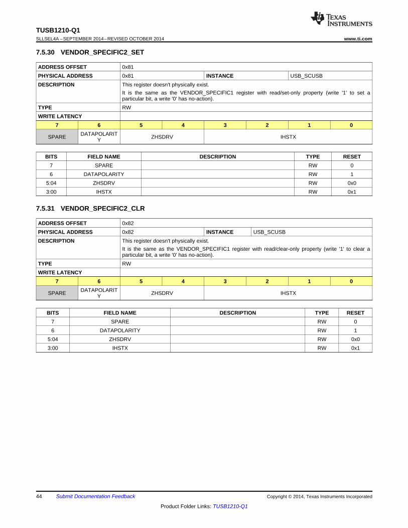
7.5.30 VENDOR_SPECIFIC2_SET
ADDRESS OFFSET 0x81PHYSICAL ADDRESS 0x81 INSTANCE USB_SCUSBDESCRIPTION This register doesn't physically exist.
It is the same as the VENDOR_SPECIFIC1 register with read/set-only property (write '1' to set aparticular bit, a write '0' has no-action).
TYPE RWWRITE LATENCY
7 6 5 4 3 2 1 0DATAPOLARITSPARE ZHSDRV IHSTXY
BITS FIELD NAME DESCRIPTION TYPE RESET7 SPARE RW 06 DATAPOLARITY RW 1
5:04 ZHSDRV RW 0x03:00 IHSTX RW 0x1
7.5.31 VENDOR_SPECIFIC2_CLR
ADDRESS OFFSET 0x82PHYSICAL ADDRESS 0x82 INSTANCE USB_SCUSBDESCRIPTION This register doesn't physically exist.
It is the same as the VENDOR_SPECIFIC1 register with read/clear-only property (write '1' to clear aparticular bit, a write '0' has no-action).
TYPE RWWRITE LATENCY
7 6 5 4 3 2 1 0DATAPOLARITSPARE ZHSDRV IHSTXY
BITS FIELD NAME DESCRIPTION TYPE RESET7 SPARE RW 06 DATAPOLARITY RW 1
5:04 ZHSDRV RW 0x03:00 IHSTX RW 0x1
44 Submit Documentation Feedback Copyright © 2014, Texas Instruments Incorporated
Product Folder Links: TUSB1210-Q1

TUSB1210-Q1www.ti.com SLLSEL4A –SEPTEMBER 2014–REVISED OCTOBER 2014
7.5.32 VENDOR_SPECIFIC1_STS
ADDRESS OFFSET 0x83PHYSICAL ADDRESS 0x83 INSTANCE USB_SCUSBDESCRIPTION Indicates the current value of the interrupt source signal.TYPE RWRITE LATEN CY
7 6 5 4 3 2 1 0MNTR_VUSBI ABNORMALST ID_FLOAT_STReserved ID_RESC_STS ID_RESB_STS ID_RESA_STS BVALID_STSN_OK_STS RESS_STS S
BITS FIELD NAME DESCRIPTION TYPE RESET7 Reserved R 06 MNTR_VUSBIN_OK_STS Current value of MNTR_VUSBIN_OK output R 05 ABNORMALSTRESS_STS Current value of ABNORMALSTRESS output R 04 ID_FLOAT_STS Current value of ID_FLOAT output R 03 ID_RESC_STS Current value of ID_RESC output R 02 ID_RESB_STS Current value of ID_RESB output R 01 ID_RESA_STS Current value of ID_RESA output R 00 BVALID_STS Current value of VB_SESS_VLD output R 0
Copyright © 2014, Texas Instruments Incorporated Submit Documentation Feedback 45
Product Folder Links: TUSB1210-Q1

TUSB1210-Q1SLLSEL4A –SEPTEMBER 2014–REVISED OCTOBER 2014 www.ti.com
7.5.33 VENDOR_SPECIFIC1_LATCH
ADDRESS OFFSET 0x84PHYSICAL ADDRESS 0x84 INSTANCE USB_SCUSBDESCRIPTION These bits are set by the PHY when an unmasked change occurs on the corresponding internal signal.
The PHY will automatically clear all bits when the Link reads this register, or when Low Power Mode isentered. The PHY also clears this register when Serial mode is entered regardless of the value ofClockSuspendM.The PHY follows the rules defined in Table 26 of the ULPI spec for setting any latch register bit.
TYPE RWRITE LATENCY
7 6 5 4 3 2 1 0MNTR_VUSBI ABNORMALST ID_FLOAT_LA ID_RESC_LAT ID_RESB_LAT ID_RESA_LAT BVALID_LATCReserved N_OK_LATCH RESS_LATCH TCH CH CH CH H
BITS FIELD NAME DESCRIPTION TYPE RESET7 Reserved R 06 MNTR_VUSBIN_OK_LATCH Set to 1 when an unmasked event occurs on MNTR_VUSBIN_OK_LATCH. R 0
Clear on read register.5 ABNORMALSTRESS_LATCH Set to 1 when an unmasked event occurs on ABNORMALSTRESS. Clear on R 0
read register.4 ID_FLOAT_LATCH Set to 1 when an unmasked event occurs on ID_FLOAT. Clear on read R 0
register.3 ID_RESC_LATCH Set to 1 when an unmasked event occurs on ID_RESC. Clear on read R 0
register.2 ID_RESB_LATCH Set to 1 when an unmasked event occurs on ID_RESB. Clear on read R 0
register.1 ID_RESA_LATCH Set to 1 when an unmasked event occurs on ID_RESA. Clear on read R 0
register.0 BVALID_LATCH Set to 1 when an unmasked event occurs on VB_SESS_VLD. Clear on read R 0
register.
46 Submit Documentation Feedback Copyright © 2014, Texas Instruments Incorporated
Product Folder Links: TUSB1210-Q1
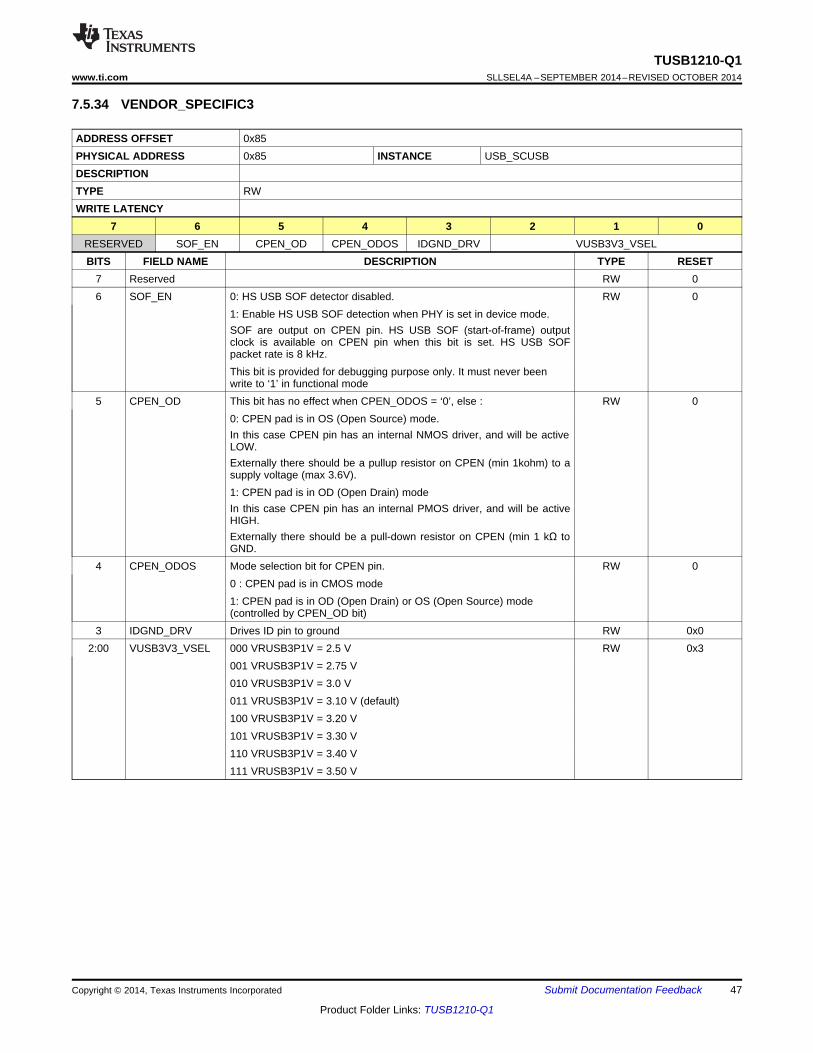
TUSB1210-Q1www.ti.com SLLSEL4A –SEPTEMBER 2014–REVISED OCTOBER 2014
7.5.34 VENDOR_SPECIFIC3
ADDRESS OFFSET 0x85PHYSICAL ADDRESS 0x85 INSTANCE USB_SCUSBDESCRIPTIONTYPE RWWRITE LATENCY
7 6 5 4 3 2 1 0RESERVED SOF_EN CPEN_OD CPEN_ODOS IDGND_DRV VUSB3V3_VSELBITS FIELD NAME DESCRIPTION TYPE RESET
7 Reserved RW 06 SOF_EN 0: HS USB SOF detector disabled. RW 0
1: Enable HS USB SOF detection when PHY is set in device mode.SOF are output on CPEN pin. HS USB SOF (start-of-frame) outputclock is available on CPEN pin when this bit is set. HS USB SOFpacket rate is 8 kHz.This bit is provided for debugging purpose only. It must never beenwrite to ‘1’ in functional mode
5 CPEN_OD This bit has no effect when CPEN_ODOS = ‘0’, else : RW 00: CPEN pad is in OS (Open Source) mode.In this case CPEN pin has an internal NMOS driver, and will be activeLOW.Externally there should be a pullup resistor on CPEN (min 1kohm) to asupply voltage (max 3.6V).1: CPEN pad is in OD (Open Drain) modeIn this case CPEN pin has an internal PMOS driver, and will be activeHIGH.Externally there should be a pull-down resistor on CPEN (min 1 kΩ toGND.
4 CPEN_ODOS Mode selection bit for CPEN pin. RW 00 : CPEN pad is in CMOS mode1: CPEN pad is in OD (Open Drain) or OS (Open Source) mode(controlled by CPEN_OD bit)
3 IDGND_DRV Drives ID pin to ground RW 0x02:00 VUSB3V3_VSEL 000 VRUSB3P1V = 2.5 V RW 0x3
001 VRUSB3P1V = 2.75 V010 VRUSB3P1V = 3.0 V011 VRUSB3P1V = 3.10 V (default)100 VRUSB3P1V = 3.20 V101 VRUSB3P1V = 3.30 V110 VRUSB3P1V = 3.40 V111 VRUSB3P1V = 3.50 V
Copyright © 2014, Texas Instruments Incorporated Submit Documentation Feedback 47
Product Folder Links: TUSB1210-Q1
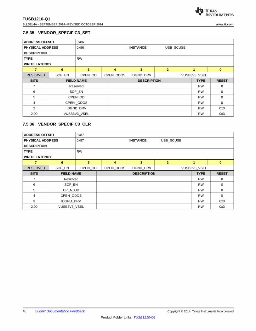
TUSB1210-Q1SLLSEL4A –SEPTEMBER 2014–REVISED OCTOBER 2014 www.ti.com
7.5.35 VENDOR_SPECIFIC3_SET
ADDRESS OFFSET 0x86PHYSICAL ADDRESS 0x86 INSTANCE USB_SCUSBDESCRIPTIONTYPE RWWRITE LATENCY
7 6 5 4 3 2 1 0RESERVED SOF_EN CPEN_OD CPEN_ODOS IDGND_DRV VUSB3V3_VSEL
BITS FIELD NAME DESCRIPTION TYPE RESET7 Reserved RW 06 SOF_EN RW 05 CPEN_OD RW 04 CPEN _ODOS RW 03 IDGND_DRV RW 0x0
2:00 VUSB3V3_VSEL RW 0x3
7.5.36 VENDOR_SPECIFIC3_CLR
ADDRESS OFFSET 0x87PHYSICAL ADDRESS 0x87 INSTANCE USB_SCUSBDESCRIPTIONTYPE RWWRITE LATENCY
7 6 5 4 3 2 1 0RESERVED SOF_EN CPEN_OD CPEN_ODOS IDGND_DRV VUSB3V3_VSEL
BITS FIELD NAME DESCRIPTION TYPE RESET7 Reserved RW 06 SOF_EN RW 05 CPEN_OD RW 04 CPEN_ODOS RW 03 IDGND_DRV RW 0x0
2:00 VUSB3V3_VSEL RW 0x3
48 Submit Documentation Feedback Copyright © 2014, Texas Instruments Incorporated
Product Folder Links: TUSB1210-Q1

(See Note A)
(See Note C)
(See Note B)
(See Note D)
TUSB1210-Q1Link Controller
VDDIO
VBUS
VBUS
EN
IN5 V OUT
VBAT
VDD33
CVDD18
CVDDIO
CBYP
CVDD33
CVDD15
CVBUS
VDD18
VDD15
7
27
5
13
12
17
4
10
VBUS Switch
USB Receptacle
ESD
3
9
29
6
2
31
GND
GND
1.8-V Supply
VDDIO Supply
3.1–5.5 VSupply
VDDIO Supply
CPEN
CS_OUT
DIR
STP
RESETB
CLOCK
CLOCK
NXT
DATA0
DATA1
DATA2
DATA3
DATA4
DATA5
DATA6
DATA7
DIR
STP
RESETB
REFCLK
NXT
DATA0
DATA1
DATA2
DATA3
DATA4
DATA5
DATA6
DATA7
1
20
21
22
26
N/C25
N/C24
N/C16
N/C15
N/C8
32
28, 30
14
11CS
CFG
18
23
19
DP
DM
ID
DP
DM
ID
SHIELD
(See Note E)
TUSB1210-Q1www.ti.com SLLSEL4A –SEPTEMBER 2014–REVISED OCTOBER 2014
8 Application and Implementation
NOTEInformation in the following applications sections is not part of the TI componentspecification, and TI does not warrant its accuracy or completeness. TI’s customers areresponsible for determining suitability of components for their purposes. Customers shouldvalidate and test their design implementation to confirm system functionality.
8.1 Application InformationFigure 5 shows the suggested application diagram (Host or OTG, ULPI input-clock mode).
8.2 Typical Application
8.2.1 Host or OTG, ULPI Input Clock Mode ApplicationFigure 5 shows a suggested application diagram for TUSB1210-Q1 in the case of ULPI input-clock mode (60MHz ULPI clock is provided by link processor), in Host or OTG application. Note this is just one example, it is ofcourse possible to operate as HOST or OTG while also in ULPI output-clock mode.
A. Pin 11 (CS) : can be tied high to VIO if CS_OUT pin unavailable; Pin 14 (CFG) : tie-high is Don’t Care since ULPIclock is used in input mode
B. Pin 1 (REFCLK) : must be tied lowC. Ext 3 V supply supportedD. Pin 27 (RESETB) can be tied to VDDIO if unused.E. Pins labeled N/C (no-connect) are truly no-connect, and can be tied or left floating.
Figure 5. Host or OTG, ULPI Input Clock Mode Application Diagram
Copyright © 2014, Texas Instruments Incorporated Submit Documentation Feedback 49
Product Folder Links: TUSB1210-Q1

TUSB1210-Q1SLLSEL4A –SEPTEMBER 2014–REVISED OCTOBER 2014 www.ti.com
Typical Application (continued)8.2.1.1 Design Requirements
Table 9. Design ParametersDESIGN PARAMETER EXAMPLE VALUE
VBAT 3.3 VVDDIO 1.8 VVBUS 5.0 V
USB Support HS, FS, LSUSB On the Go (OTG) Yes
Clock Sources 60 MHz Clock
8.2.1.2 Detailed Design ProcedureConnect the TUSB1210 device as is shown in Figure 5.
Follow the Board Guidelines of the Application Report, SWCA124.
8.2.1.2.1 Unused Pins Connection
• VBUS: Input. Recommended to tie to GND if unused. However leaving VBUS floating is also acceptable sinceinternally there is an 80 kΩ resistance to ground.
• REFCLK: Input. If REFCLK is unused, and 60 MHz clock is provided by MODEM (60 MHz should beconnected to CLOCK pin in this case) then tie REFCLK to GND.
• CFG: Tie to GND if REFCLK is 19.2MHz, or tie to VDDIO if REFCLK is 26 MHz. Tie to either GND or VDDIO(doesn't matter which) if REFCLK not used (i.e., ULPI input clock configuration).
8.2.1.3 Application Curve
Figure 6. High-Speed Eye Diagram
50 Submit Documentation Feedback Copyright © 2014, Texas Instruments Incorporated
Product Folder Links: TUSB1210-Q1
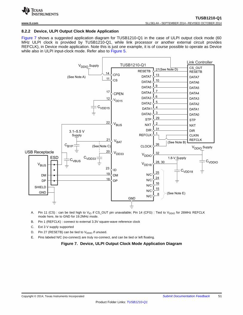
(See Note A)
(See Note C)
(See Note B)
(See Note E)
(See Note D)
TUSB1210-Q1Link Controller
VDDIO
VBUS
VBUS
VBAT
VDD33
CVDD18
CVDDIO
CBYP
CVDD33
CVDD15
CVBUSVDD18
VDD15
7
27
5
13
12
17
4
10
USB Receptacle
ESD
3
9
29
6
2
GND
GND
1.8-V Supply
VDDIO Supply
3.1–5.5 VSupply
VDDIO Supply
CPEN
CS_OUT
STP
RESETB
REFCLK
CLOCK
NXT
DATA0
DATA1
DATA2
DATA3
DATA4
DATA5
DATA6
DATA7
STP
RESETB
REFCLK
NXT
DATA0
DATA1
DATA2
DATA3
DATA4
DATA5
DATA6
DATA7
20
21
22
26
32
28, 30
31DIRDIR
1CLKIN
14
11CS
CFG
18
23
19
DP
DM
ID
DP
DM
SHIELD
N/C25
N/C24
N/C16
N/C15
N/C8
TUSB1210-Q1www.ti.com SLLSEL4A –SEPTEMBER 2014–REVISED OCTOBER 2014
8.2.2 Device, ULPI Output Clock Mode ApplicationFigure 7 shows a suggested application diagram for TUSB1210-Q1 in the case of ULPI output clock mode (60MHz ULPI clock is provided by TUSB1210-Q1, while link processor or another external circuit providesREFCLK), in Device mode application. Note this is just one example, it is of course possible to operate as Devicewhile also in ULPI input-clock mode. Refer also to Figure 5.
A. Pin 11 (CS) : can be tied high to VIO if CS_OUT pin unavailable; Pin 14 (CFG) : Tied to VDDIO for 26MHz REFCLKmode here, tie to GND for 19.2MHz mode.
B. Pin 1 (REFCLK) : connect to external 3.3V square-wave reference clockC. Ext 3 V supply supportedD. Pin 27 (RESETB) can be tied to VDDIO if unused.E. Pins labeled N/C (no-connect) are truly no-connect, and can be tied or left floating.
Figure 7. Device, ULPI Output Clock Mode Application Diagram
Copyright © 2014, Texas Instruments Incorporated Submit Documentation Feedback 51
Product Folder Links: TUSB1210-Q1
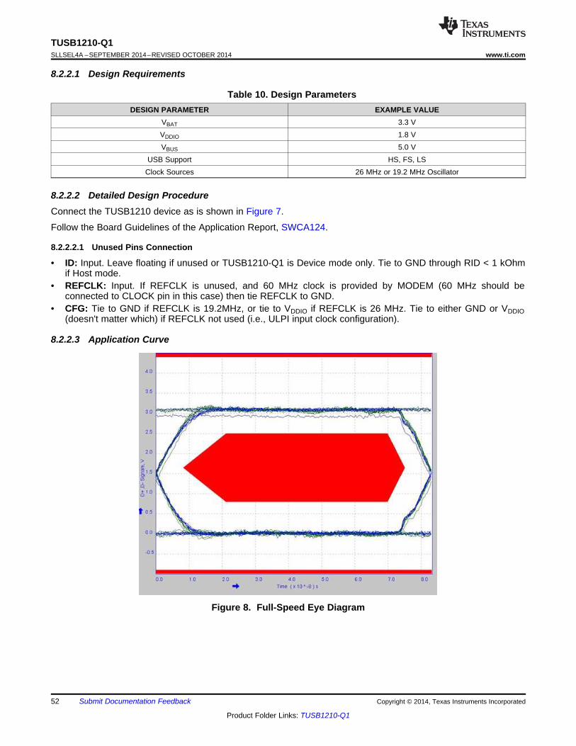
TUSB1210-Q1SLLSEL4A –SEPTEMBER 2014–REVISED OCTOBER 2014 www.ti.com
8.2.2.1 Design Requirements
Table 10. Design ParametersDESIGN PARAMETER EXAMPLE VALUE
VBAT 3.3 VVDDIO 1.8 VVBUS 5.0 V
USB Support HS, FS, LSClock Sources 26 MHz or 19.2 MHz Oscillator
8.2.2.2 Detailed Design ProcedureConnect the TUSB1210 device as is shown in Figure 7.
Follow the Board Guidelines of the Application Report, SWCA124.
8.2.2.2.1 Unused Pins Connection
• ID: Input. Leave floating if unused or TUSB1210-Q1 is Device mode only. Tie to GND through RID < 1 kOhmif Host mode.
• REFCLK: Input. If REFCLK is unused, and 60 MHz clock is provided by MODEM (60 MHz should beconnected to CLOCK pin in this case) then tie REFCLK to GND.
• CFG: Tie to GND if REFCLK is 19.2MHz, or tie to VDDIO if REFCLK is 26 MHz. Tie to either GND or VDDIO(doesn't matter which) if REFCLK not used (i.e., ULPI input clock configuration).
8.2.2.3 Application Curve
Figure 8. Full-Speed Eye Diagram
52 Submit Documentation Feedback Copyright © 2014, Texas Instruments Incorporated
Product Folder Links: TUSB1210-Q1

TUSB1210-Q1www.ti.com SLLSEL4A –SEPTEMBER 2014–REVISED OCTOBER 2014
8.3 External Components
Table 11. TUSB1210-Q1 External ComponentsFUNCTION COMPONENT REFERENCE VALUE NOTE LINK
VDDIO Capacitor CVDDIO 100 nF Suggested value, application Figure 5dependent
VDD33 Capacitor CVDD33 2.2 μF Range: [0.45 μF : 6.5 μF] , Figure 5ESR = [0 : 600 mΩ] for f> 10 kHz
VDD15 Capacitor CVDD15 2.2 μF Range: [0.45 μF : 6.5 μF] , Figure 5ESR = [0 : 600 mΩ] for f> 10 kHz
VDD18 Capacitor Ext 1.8V supply 100 nF Suggested value, application Figure 5dependentCVDD18
VBAT Capacitor CBYP 100 nF (1) Range: [0.45 μF : 6.5 μF] , Figure 5ESR = [0 : 600 mΩ] for f> 10 kHz
VBUS Capacitor CVBUS See Table 12 Place close to USB connector Figure 5
(1) Recommended value but 2.2 uF may be sufficient in some applications
Table 12. TUSB1210-Q1 VBUS CapacitorsFUNCTION COMPONENT REFERENCE VALUE NOTE LINK
VBUS - HOST Capacitor CVBUS >120 μF Figure 5VBUS – DEVICE Capacitor CVBUS 4.7 μF Range: 1.0 μF to 10.0 μF Figure 5
VBUS - OTG Capacitor CVBUS 4.7 μF Range: 1.0 μF to 6.5 μF Figure 5
Copyright © 2014, Texas Instruments Incorporated Submit Documentation Feedback 53
Product Folder Links: TUSB1210-Q1

TUSB1210-Q1SLLSEL4A –SEPTEMBER 2014–REVISED OCTOBER 2014 www.ti.com
9 Power Supply RecommendationsVBUS, and VBAT, and VDDIO, are needed for power the TUSB1210-Q1. Recommended operation is for VBAT to bepresent before VDDIO. Applying VDDIO before VBAT to TUSB1210 is not recommended as there is a diode fromVDDIO to VBAT which will be forward biased when VDDIO is present but VBAT is not present. TUSB1210-Q1 doesnot strictly require VBUS to function.
9.1 TUSB1210 Power Supply• The VDDIO pins of the TUSB1210-Q1 supply 1.8 V (nominal) power to the core of the TUSB1210-Q1. This
power rail can be isolated from all other power rails by a ferrite bead to reduce noise.• The VBAT pin of the TUSB1210-Q1 supply 3.3 V (nominal) power rail to the TUSB1210-Q1. This power rail
can be isolated from all other power rails by a ferrite bead to reduce noise.• The VBUS pin of the TUSB1210-Q1 supply 5.0 V (nominal) power rail to the TUSB1210-Q1. This pin is
normally connected to the VBUS pin of the USB connector.• The VBUS pin of the TUSB1210-Q1 supply 5.0 V (nominal) power rail to the TUSB1210-Q1. This pin is
normally connected to the VBUS pin of the USB connector.
9.2 GroundIt is recommended that almost one board ground plane be used in the design. This provides the best imageplane for signal traces running above the plane. An earth or chassis ground is implemented only near the USBport connectors on a different plane for EMI and ESD purposes.
9.3 Power ProvidersTable 13 is a summary of TUSB1210-Q1 power providers.
Table 13. Power Providers (1)
TYPICAL MAXIMUMNAME USAGE TYPE VOLTAGE (V) CURRENT (mA)VDD15 Internal LDO 1.5 50VDD18 External LDO 1.8 30VDD33 Internal LDO 3.1 15
(1) VDD33 may be supplied externally, or by shorting the VDD33 pin to VBAT pin provided VBAT min is inrange [3.2 V : 3.6 V]. Note that the VDD33 LDO will always power-on when the chip is enabled,irrespective of whether VDD33 is supplied externally or not. In the case the VDD33 pin is not suppliedexternally in the application, the electrical specs for this LDO are provided below.
9.4 Power Modules
9.4.1 VDD33 RegulatorThe VDD33 internal LDO regulator powers the USB PHY, charger detection, and OTG functions of the USBsubchip inside TUSB1210-Q1. Power Characteristics describes the regulator characteristics.
VDD33 regulator takes its power from VBAT.
Since the USB2.0 standard requires data lines to be biased with pullups biased from a supply greater than 3 V,and since VDD33 regulator has an inherent voltage drop from its input, VBAT, to its regulated output, TUSB1210-Q1 will not meet USB 2.0 Standard if operated from a battery whose voltage is lower than3.3 V.
9.4.2 VDD18 SupplyThe VDD18 supply is powered externally at the VDD18 pin. See Table 11 for external components.
9.4.3 VDD15 RegulatorThe VDD15 internal LDO regulator powers the USB subchip inside TUSB1210-Q1. Power Characteristicsdescribes the regulator characteristics.
54 Submit Documentation Feedback Copyright © 2014, Texas Instruments Incorporated
Product Folder Links: TUSB1210-Q1

TUSB1210-Q1www.ti.com SLLSEL4A –SEPTEMBER 2014–REVISED OCTOBER 2014
9.5 Power ConsumptionTable 14 describes the power consumption depending on the use cases.
NOTEThe typical power consumption is obtained in the nominal operating conditions and withthe TUSB1210-Q1 standalone.
Table 14. Power ConsumptionTYPICALMODE CONDITIONS SUPPLY UNITCONSUMPTION
IVBAT 8IVDDIO 3VBAT = 3.6 V, VDDIO = 1.8 V, VDD18OFF Mode µA= 1.8 V, CS = 0 V IVDD18 5ITOTAL 16IVBAT 204IVDDIO 3VBUS = 5 V, VBAT = 3.6 V, VDDIO =Suspend Mode µA1.8 V, No clock IVDD18 3ITOTAL 210IVBAT 24.6IVDDIO 1.89HS USB Operation VBAT = 3.6 V, VDDIO = 1.8 V, VDD18 mA(Synchronous Mode) = 1.8 V, active USB transfer IVDD18 21.5ITOTAL 48IVBAT 25.8IVDDIO 1.81FS USB Operation VBAT = 3.6 V, VDDIO = 1.8 V, active mA(Synchronous Mode) USB transfer IVDD18 4.06ITOTAL 31.7IVBAT 237IVDDIO 3RESETB = 0 V, VBUS = 5 V, VBATReset Mode µA= 3.6 V, VDDIO = 1.8 V, No clock IVDD18 3ITOTAL 243
Copyright © 2014, Texas Instruments Incorporated Submit Documentation Feedback 55
Product Folder Links: TUSB1210-Q1

TUSB1210-Q1SLLSEL4A –SEPTEMBER 2014–REVISED OCTOBER 2014 www.ti.com
10 Layout
10.1 Layout Guidelines• The VDDIO pins of the TUSB1210-Q1 supply 1.8-V (nominal) power to the core of the TUSB1210-Q1. This
power rail can be isolated from all other power rails by a ferrite bead to reduce noise.• The VBAT pin of the TUSB1210-Q1 supply 3.3-V (nominal) power rail to the TUSB1210-Q1. This power rail
can be isolated from all other power rails by a ferrite bead to reduce noise.• The VBUS pin of the TUSB1210-Q1 supply 5-V (nominal) power rail to the TUSB1210-Q1. This pin is normally
connected to the VBUS pin of the USB connector.• All power rails require 0.1 μF decoupling capacitors for stability and noise immunity. The smaller decoupling
capacitors should be placed as close to the TUSB1210-Q1 power pins as possible with an optimal groupingof two of differing values per pin.
10.2 Layout Example
Figure 9. TUSB1210-Q1 Layout Example
56 Submit Documentation Feedback Copyright © 2014, Texas Instruments Incorporated
Product Folder Links: TUSB1210-Q1
TUSB1210-Q1www.ti.com SLLSEL4A –SEPTEMBER 2014–REVISED OCTOBER 2014
11 Device and Documentation Support
11.1 Documentation SupportSLLZ066 Silicon Errata. Describes the known exceptions to the functional specifications for the TUSB1210-
Q1.
11.2 Community ResourcesThe following links connect to TI community resources. Linked contents are provided "AS IS" by the respectivecontributors. They do not constitute TI specifications and do not necessarily reflect TI's views; see TI's Terms ofUse.
TI E2E™ Online Community TI's Engineer-to-Engineer (E2E) Community. Created to foster collaborationamong engineers. At e2e.ti.com, you can ask questions, share knowledge, explore ideas and helpsolve problems with fellow engineers.
TI Embedded Processors Wiki Texas Instruments Embedded Processors Wiki. Established to helpdevelopers get started with Embedded Processors from Texas Instruments and to foster innovationand growth of general knowledge about the hardware and software surrounding these devices.
11.3 TrademarksE2E is a trademark of Texas Instruments.All other trademarks are the property of their respective owners.
11.4 Electrostatic Discharge CautionThis integrated circuit can be damaged by ESD. Texas Instruments recommends that all integrated circuits be handled withappropriate precautions. Failure to observe proper handling and installation procedures can cause damage.
ESD damage can range from subtle performance degradation to complete device failure. Precision integrated circuits may be moresusceptible to damage because very small parametric changes could cause the device not to meet its published specifications.
11.5 Glossary
11.5.1 GlossarySLYZ022 — TI Glossary.
This glossary lists and explains terms, acronyms, and definitions.
Copyright © 2014, Texas Instruments Incorporated Submit Documentation Feedback 57
Product Folder Links: TUSB1210-Q1

TUSB1210-Q1SLLSEL4A –SEPTEMBER 2014–REVISED OCTOBER 2014 www.ti.com
12 Mechanical, Packaging, and Orderable Information
12.1 Via ChannelThe T package has been specially engineered with Via Channel technology. This allows larger than normal PCBvia and trace sizes and reduced PCB signal layers to be used in a PCB design with the 0.65-mm pitch package,and substantially reduces PCB costs. It allows PCB routing in only two signal layers (four layers total) due to theincreased layer efficiency of the Via Channel BGA technology.
Via Channel technology implemented on the [your package] package makes it possible to build an [your device]-based product with a 4-layer PCB, but a 4-layer PCB may not meet system performance goals. Therefore,system performance using a 4-layer PCB design must be evaluated during product design.
12.2 Packaging InformationThe following pages include mechanical packaging and orderable information. This information is the mostcurrent data available for the designated devices. This data is subject to change without notice and revision ofthis document. For browser-based versions of this data sheet, refer to the left-hand navigation.
58 Submit Documentation Feedback Copyright © 2014, Texas Instruments Incorporated
Product Folder Links: TUSB1210-Q1

PACKAGE OPTION ADDENDUM
www.ti.com 7-Oct-2014
Addendum-Page 1
PACKAGING INFORMATION
Orderable Device Status(1)
Package Type PackageDrawing
Pins PackageQty
Eco Plan(2)
Lead/Ball Finish(6)
MSL Peak Temp(3)
Op Temp (°C) Device Marking(4/5)
Samples
TUSB1210BRHBRQ1 ACTIVE VQFN RHB 32 3000 Green (RoHS& no Sb/Br)
CU NIPDAU Level-2-260C-1 YEAR -40 to 85 T1210Q1
TUSB1210BRHBTQ1 ACTIVE VQFN RHB 32 250 Green (RoHS& no Sb/Br)
CU NIPDAU Level-2-260C-1 YEAR -40 to 85 T1210Q1
(1) The marketing status values are defined as follows:ACTIVE: Product device recommended for new designs.LIFEBUY: TI has announced that the device will be discontinued, and a lifetime-buy period is in effect.NRND: Not recommended for new designs. Device is in production to support existing customers, but TI does not recommend using this part in a new design.PREVIEW: Device has been announced but is not in production. Samples may or may not be available.OBSOLETE: TI has discontinued the production of the device.
(2) Eco Plan - The planned eco-friendly classification: Pb-Free (RoHS), Pb-Free (RoHS Exempt), or Green (RoHS & no Sb/Br) - please check http://www.ti.com/productcontent for the latest availabilityinformation and additional product content details.TBD: The Pb-Free/Green conversion plan has not been defined.Pb-Free (RoHS): TI's terms "Lead-Free" or "Pb-Free" mean semiconductor products that are compatible with the current RoHS requirements for all 6 substances, including the requirement thatlead not exceed 0.1% by weight in homogeneous materials. Where designed to be soldered at high temperatures, TI Pb-Free products are suitable for use in specified lead-free processes.Pb-Free (RoHS Exempt): This component has a RoHS exemption for either 1) lead-based flip-chip solder bumps used between the die and package, or 2) lead-based die adhesive used betweenthe die and leadframe. The component is otherwise considered Pb-Free (RoHS compatible) as defined above.Green (RoHS & no Sb/Br): TI defines "Green" to mean Pb-Free (RoHS compatible), and free of Bromine (Br) and Antimony (Sb) based flame retardants (Br or Sb do not exceed 0.1% by weightin homogeneous material)
(3) MSL, Peak Temp. - The Moisture Sensitivity Level rating according to the JEDEC industry standard classifications, and peak solder temperature.
(4) There may be additional marking, which relates to the logo, the lot trace code information, or the environmental category on the device.
(5) Multiple Device Markings will be inside parentheses. Only one Device Marking contained in parentheses and separated by a "~" will appear on a device. If a line is indented then it is a continuationof the previous line and the two combined represent the entire Device Marking for that device.
(6) Lead/Ball Finish - Orderable Devices may have multiple material finish options. Finish options are separated by a vertical ruled line. Lead/Ball Finish values may wrap to two lines if the finishvalue exceeds the maximum column width.
Important Information and Disclaimer:The information provided on this page represents TI's knowledge and belief as of the date that it is provided. TI bases its knowledge and belief on informationprovided by third parties, and makes no representation or warranty as to the accuracy of such information. Efforts are underway to better integrate information from third parties. TI has taken andcontinues to take reasonable steps to provide representative and accurate information but may not have conducted destructive testing or chemical analysis on incoming materials and chemicals.TI and TI suppliers consider certain information to be proprietary, and thus CAS numbers and other limited information may not be available for release.
PACKAGE OPTION ADDENDUM
www.ti.com 7-Oct-2014
Addendum-Page 2
In no event shall TI's liability arising out of such information exceed the total purchase price of the TI part(s) at issue in this document sold by TI to Customer on an annual basis.
OTHER QUALIFIED VERSIONS OF TUSB1210-Q1 :
• Catalog: TUSB1210
NOTE: Qualified Version Definitions:
• Catalog - TI's standard catalog product

TAPE AND REEL INFORMATION
*All dimensions are nominal
Device PackageType
PackageDrawing
Pins SPQ ReelDiameter
(mm)
ReelWidth
W1 (mm)
A0(mm)
B0(mm)
K0(mm)
P1(mm)
W(mm)
Pin1Quadrant
TUSB1210BRHBRQ1 VQFN RHB 32 3000 330.0 12.4 5.3 5.3 1.1 8.0 12.0 Q2
TUSB1210BRHBTQ1 VQFN RHB 32 250 180.0 12.4 5.3 5.3 1.1 8.0 12.0 Q2
PACKAGE MATERIALS INFORMATION
www.ti.com 3-Aug-2017
Pack Materials-Page 1

*All dimensions are nominal
Device Package Type Package Drawing Pins SPQ Length (mm) Width (mm) Height (mm)
TUSB1210BRHBRQ1 VQFN RHB 32 3000 367.0 367.0 35.0
TUSB1210BRHBTQ1 VQFN RHB 32 250 210.0 185.0 35.0
PACKAGE MATERIALS INFORMATION
www.ti.com 3-Aug-2017
Pack Materials-Page 2
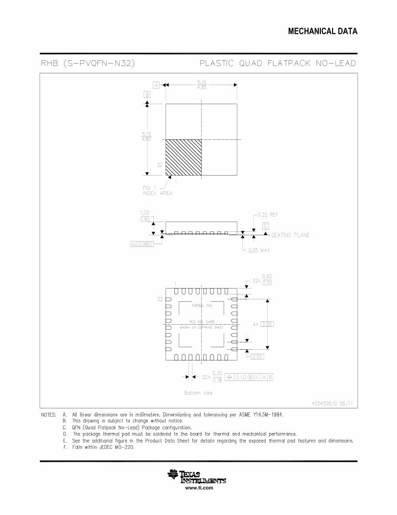
IMPORTANT NOTICE
Texas Instruments Incorporated (TI) reserves the right to make corrections, enhancements, improvements and other changes to itssemiconductor products and services per JESD46, latest issue, and to discontinue any product or service per JESD48, latest issue. Buyersshould obtain the latest relevant information before placing orders and should verify that such information is current and complete.TI’s published terms of sale for semiconductor products (http://www.ti.com/sc/docs/stdterms.htm) apply to the sale of packaged integratedcircuit products that TI has qualified and released to market. Additional terms may apply to the use or sale of other types of TI products andservices.Reproduction of significant portions of TI information in TI data sheets is permissible only if reproduction is without alteration and isaccompanied by all associated warranties, conditions, limitations, and notices. TI is not responsible or liable for such reproduceddocumentation. Information of third parties may be subject to additional restrictions. Resale of TI products or services with statementsdifferent from or beyond the parameters stated by TI for that product or service voids all express and any implied warranties for theassociated TI product or service and is an unfair and deceptive business practice. TI is not responsible or liable for any such statements.Buyers and others who are developing systems that incorporate TI products (collectively, “Designers”) understand and agree that Designersremain responsible for using their independent analysis, evaluation and judgment in designing their applications and that Designers havefull and exclusive responsibility to assure the safety of Designers' applications and compliance of their applications (and of all TI productsused in or for Designers’ applications) with all applicable regulations, laws and other applicable requirements. Designer represents that, withrespect to their applications, Designer has all the necessary expertise to create and implement safeguards that (1) anticipate dangerousconsequences of failures, (2) monitor failures and their consequences, and (3) lessen the likelihood of failures that might cause harm andtake appropriate actions. Designer agrees that prior to using or distributing any applications that include TI products, Designer willthoroughly test such applications and the functionality of such TI products as used in such applications.TI’s provision of technical, application or other design advice, quality characterization, reliability data or other services or information,including, but not limited to, reference designs and materials relating to evaluation modules, (collectively, “TI Resources”) are intended toassist designers who are developing applications that incorporate TI products; by downloading, accessing or using TI Resources in anyway, Designer (individually or, if Designer is acting on behalf of a company, Designer’s company) agrees to use any particular TI Resourcesolely for this purpose and subject to the terms of this Notice.TI’s provision of TI Resources does not expand or otherwise alter TI’s applicable published warranties or warranty disclaimers for TIproducts, and no additional obligations or liabilities arise from TI providing such TI Resources. TI reserves the right to make corrections,enhancements, improvements and other changes to its TI Resources. TI has not conducted any testing other than that specificallydescribed in the published documentation for a particular TI Resource.Designer is authorized to use, copy and modify any individual TI Resource only in connection with the development of applications thatinclude the TI product(s) identified in such TI Resource. NO OTHER LICENSE, EXPRESS OR IMPLIED, BY ESTOPPEL OR OTHERWISETO ANY OTHER TI INTELLECTUAL PROPERTY RIGHT, AND NO LICENSE TO ANY TECHNOLOGY OR INTELLECTUAL PROPERTYRIGHT OF TI OR ANY THIRD PARTY IS GRANTED HEREIN, including but not limited to any patent right, copyright, mask work right, orother intellectual property right relating to any combination, machine, or process in which TI products or services are used. Informationregarding or referencing third-party products or services does not constitute a license to use such products or services, or a warranty orendorsement thereof. Use of TI Resources may require a license from a third party under the patents or other intellectual property of thethird party, or a license from TI under the patents or other intellectual property of TI.TI RESOURCES ARE PROVIDED “AS IS” AND WITH ALL FAULTS. TI DISCLAIMS ALL OTHER WARRANTIES ORREPRESENTATIONS, EXPRESS OR IMPLIED, REGARDING RESOURCES OR USE THEREOF, INCLUDING BUT NOT LIMITED TOACCURACY OR COMPLETENESS, TITLE, ANY EPIDEMIC FAILURE WARRANTY AND ANY IMPLIED WARRANTIES OFMERCHANTABILITY, FITNESS FOR A PARTICULAR PURPOSE, AND NON-INFRINGEMENT OF ANY THIRD PARTY INTELLECTUALPROPERTY RIGHTS. TI SHALL NOT BE LIABLE FOR AND SHALL NOT DEFEND OR INDEMNIFY DESIGNER AGAINST ANY CLAIM,INCLUDING BUT NOT LIMITED TO ANY INFRINGEMENT CLAIM THAT RELATES TO OR IS BASED ON ANY COMBINATION OFPRODUCTS EVEN IF DESCRIBED IN TI RESOURCES OR OTHERWISE. IN NO EVENT SHALL TI BE LIABLE FOR ANY ACTUAL,DIRECT, SPECIAL, COLLATERAL, INDIRECT, PUNITIVE, INCIDENTAL, CONSEQUENTIAL OR EXEMPLARY DAMAGES INCONNECTION WITH OR ARISING OUT OF TI RESOURCES OR USE THEREOF, AND REGARDLESS OF WHETHER TI HAS BEENADVISED OF THE POSSIBILITY OF SUCH DAMAGES.Unless TI has explicitly designated an individual product as meeting the requirements of a particular industry standard (e.g., ISO/TS 16949and ISO 26262), TI is not responsible for any failure to meet such industry standard requirements.Where TI specifically promotes products as facilitating functional safety or as compliant with industry functional safety standards, suchproducts are intended to help enable customers to design and create their own applications that meet applicable functional safety standardsand requirements. Using products in an application does not by itself establish any safety features in the application. Designers mustensure compliance with safety-related requirements and standards applicable to their applications. Designer may not use any TI products inlife-critical medical equipment unless authorized officers of the parties have executed a special contract specifically governing such use.Life-critical medical equipment is medical equipment where failure of such equipment would cause serious bodily injury or death (e.g., lifesupport, pacemakers, defibrillators, heart pumps, neurostimulators, and implantables). Such equipment includes, without limitation, allmedical devices identified by the U.S. Food and Drug Administration as Class III devices and equivalent classifications outside the U.S.TI may expressly designate certain products as completing a particular qualification (e.g., Q100, Military Grade, or Enhanced Product).Designers agree that it has the necessary expertise to select the product with the appropriate qualification designation for their applicationsand that proper product selection is at Designers’ own risk. Designers are solely responsible for compliance with all legal and regulatoryrequirements in connection with such selection.Designer will fully indemnify TI and its representatives against any damages, costs, losses, and/or liabilities arising out of Designer’s non-compliance with the terms and provisions of this Notice.
Mailing Address: Texas Instruments, Post Office Box 655303, Dallas, Texas 75265Copyright © 2017, Texas Instruments Incorporated

![Announces Q4 & FY16 Results (Standalone), Form A (Standalone) & Auditors Report (Standalone) for the period ended March 31, 2016 [Result]](https://static.fdocuments.us/doc/165x107/577c7af51a28abe05496b138/announces-q4-fy16-results-standalone-form-a-standalone-auditors-report.jpg)


![Pcp standalone [autosaved]](https://static.fdocuments.us/doc/165x107/55a251601a28abd1758b45fc/pcp-standalone-autosaved.jpg)


![Announces FY16 Results (Standalone & Consolidated), Form A (Standalone & Consolidated) & Auditors Report (Standalone & Consolidated) for the period ended March 31, 2016 [Result]](https://static.fdocuments.us/doc/165x107/577c7c7c1a28abe0549ac98f/announces-fy16-results-standalone-consolidated-form-a-standalone-consolidated.jpg)