
SKYLIGHT LIGHT INTENSITY LOGGING
12
Active and Passive Elec. Comp., 1997, Vol. 20, pp. 7-17 Reprints available directly from the publisher Photocopying permitted by license only (C) 1997 OPA (Overseas Publishers Association) Amsterdam B.V. Published in The Netherlands under license by Gordon and Breach Science Publishers Printed in Malaysia SKYLIGHT LIGHT INTENSITY DATA LOGGING SYSTEM A. UDINA and LC JAIN* ICES, University of South Australia Warrendi Road, The Levels South Autralia, 5095 Australia (Received 12 February 1996; In final form 29 March 1996) The design of a skylight intensity data logging system is presented. The proposed system is able to accept 32 inputs in two 16 input blocks with capabilities for further expansion. A typical application would be to simultaneously monitor real time change in light intensity in two skylight units, over a chosen periods of minutes, hours or days. INTRODUCTION Skylights and skylight systems have grown in size and flexibility over the last 15 years. Many so-called improved systems have gained market at- tention and the quest is always out to improve the useful light capturing abilities of skylights. Yet there has been very little if any generally pub- lished scientific data on the light capturing and transmitting capabilities of the various systems on the market. Qualitatively one system is pronounced as being better than another system, but it is never stated by how much. As a first step in addressing this gap in the industry knowledge, a light intensity data logging system was designed for the surveillance of light intensity within a skylight duct. Although data logging systems are not new and indeed lux meters have been around for a long time, the problem posed in this situation was the large range of light intensities encountered. The intensity ranges from a few lux to approximately 100,000 lux or 5 decades. *Corresponding author.
Transcript of SKYLIGHT LIGHT INTENSITY LOGGING
Active and Passive Elec. Comp., 1997, Vol. 20, pp. 7-17Reprints available directly from the publisherPhotocopying permitted by license only
(C) 1997 OPA (Overseas Publishers Association)Amsterdam B.V. Published in The Netherlands
under license by Gordon and Breach Science Publishers
Printed in Malaysia
SKYLIGHT LIGHT INTENSITY DATALOGGING SYSTEM
A. UDINA and LC JAIN*
ICES, University of South Australia Warrendi Road, The LevelsSouth Autralia, 5095 Australia
(Received 12 February 1996; In final form 29 March 1996)
The design of a skylight intensity data logging system is presented. The proposed system isable to accept 32 inputs in two 16 input blocks with capabilities for further expansion. Atypical application would be to simultaneously monitor real time change in light intensity intwo skylight units, over a chosen periods of minutes, hours or days.
INTRODUCTION
Skylights and skylight systems have grown in size and flexibility over thelast 15 years. Many so-called improved systems have gained market at-tention and the quest is always out to improve the useful light capturingabilities of skylights. Yet there has been very little if any generally pub-lished scientific data on the light capturing and transmitting capabilities ofthe various systems on the market. Qualitatively one system is pronouncedas being better than another system, but it is never stated by how much.As a first step in addressing this gap in the industry knowledge, a light
intensity data logging system was designed for the surveillance of lightintensity within a skylight duct. Although data logging systems are not newand indeed lux meters have been around for a long time, the problem posedin this situation was the large range of light intensities encountered. Theintensity ranges from a few lux to approximately 100,000 lux or 5 decades.
*Corresponding author.
8 A. UDINA and LC JAIN
In general, lux meters that are capable of measuring over that rangehave two or three ranging resistors that provide the correct ranging. Theseresistors are generally positioned in a feedback circuit of a current-to-
voltage converter. The problem with using this system is that every rang-ing change will produce a discontinuity across which the output will alsobe discontinuous. This is due to the different resistors not possessing thesame characteristics; hence when a resistor is changed the circuit charac-teristics and thus the transfer function is also altered. No matter how goodthe individual elements are, these effects will always be encountered.
This paper describes a design utilizing known technology in providing a
simple solution to the described design limitation. Furthermore, this de-sign is able to accept 32 inputs in two 16 input blocks with capabilities forfurther expansion. A typical application would be to simultaneously moni-tor real time change in light intensity in two skylight units, over a chosenperiod of minutes, hours, or even days. The system is portable and can beplugged into the printer port of any IBM compatible Personal Computer. Itcan also monitor the performance of a permanently installed skylight sys-tem.
THE PRINCIPLE OF OPERATION
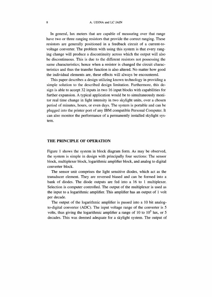
Figure 1 shows the system in block diagram form. As may be observed,the system is simple in design with principally four sections: The sensor
block, multiplexer block, logarithmic amplifier block, and analog to digitalconverter block.The sensor unit comprises the light sensitive diodes, which act as the
transducer element. They are reversed biased and can be formed into abank of diodes. The diode outputs are fed into a 16 to 1 multiplexer.Selection is computer controlled. The output of the multiplexer is used as
the input to a logarithmic amplifier. This amplifier has an output of 1 voltper decade.The output of the logarithmic amplifier is passed into a 10 bit analog-
to-digital converter (ADC). The input voltage range of the converter is 5volts, thus giving the logarithmic amplifier a range of 10 to 105 lux, or 5decades. This was deemed adequate for a skylight system. The output of
LIGHT INTENSITY DATA LOGGING 9
FIGURE
converer
Block Diagram of Sensor Circuit.
ToComputer
the ADC is then passed in 4 bit words to a Personal Computer. Here thedata is stored for later processing.
DETAILED DESCRIPTION
Sensor Elements
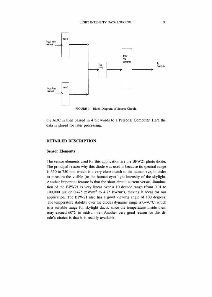
The sensor elements used for this application are the BPW21 photo diode.The principal reason why this diode was used is because its spectral rangeis 350 to 750 nm, which is a very close match to the human eye, in orderto measure the visible (to the human eye) light intensity of the skylight.Another important feature is that the short circuit current versus illumina-tion of the BPW21 is very linear over a 10 decade range (from 0.01 to
100,000 lux or 0.475 mW/m2 to 4.75 kW/m2), making it ideal for our
application. The BPW21 also has a good viewing angle of 100 degrees.The temperature stability over the diodes dynamic range is 0-70C, whichis a suitable range for skylight ducts, since the temperature inside themmay exceed 60C in midsummer. Another very good reason for this di-ode’s choice is that it is readily available.
10 A. UDINA and LC JAIN
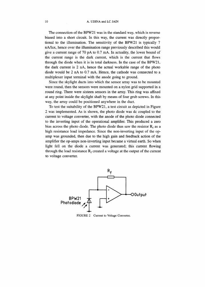
The connection of the BPW21 was in the standard way, which is reversebiased into a short circuit. In this way, the current was directly propor-tional to the illumination. The sensitivity of the BPW21 is typically 7nA/lux, hence over the illumination range previously described this wouldgive a current range of 70 pA to 0.7 mA. In actuality, the lower bound ofthe current range is the dark current, which is the current that flowsthrough the diode when it is in total darkness. In the case of the BPW21,the dark current is 2 nA, hence the actual workable range of the photodiode would be 2 nA to 0.7 mA. Hence, the cathode was connected to a
multiplexer input terminal with the anode going to ground.Since the skylight ducts into which the sensor array was to be mounted
were round, then the sensors were mounted on a nylon grid supported in around ring. There were sixteen sensors in the array. This ring was affixedat any point inside the skylight shaft by means of four grub screws. In thisway, the array could be positioned anywhere in the duct.To test the suitability of the BPW21, a test circuit as depicted in Figure
2 was implemented. As is shown, the photo diode was dc coupled to thecurrent to voltage converter, with the anode of the photo diode connectedto the inverting input of the operational amplifier. This produced a zerobias across the photo diode. The photo diode thus saw the resistor Rf as ahigh resistance load impedance. Since the non-inverting input of the op-amp was grounded, then due to the high gain and feedback action of theamplifier the op-amps non-inverting input became a virtual earth. So whenlight fell on the diode a current was generated; this current flowingthrough the load resistance Rf created a voltage at the output of the currentto voltage converter.
8PW21Photodiode
"--OOutput
FIGURE 2 Current to Voltage Converter.
LIGHT INTENSITY DATA LOGGING 11
Multiplexers
There were a number of considerations that were needed for the multi-
plexers, which were as follows:
1) Number of channels. Since we had 16 sensors to a block, we needed 16inputs. The question was to use either a 16 channel multiplexer or two8 channel multiplexers. Price expediency dictated the two 8 channeloption.
2) Dynamic Range. As we established earlier, the output from the sensorscould range from 2 nA to 0.7 mA, thus we needed analog multiplexers,which would be capable of handling the very low currents.
3) Degree of Crosstalk. Again, since we were dealing with low currentswe needed a multiplexer that was quiet enough to allow the input for achannel to not be affected by what may be on any other channel.
4) Degree of Transfer error. As with the previous considerations, the noise
figure of the multiplexer would have to be low enough so as to not
degenerate the signal beyond recognition.
The multiplexer chosen was the MUX4067. These devices are cheap,popular, and pass all the selection criteria.One main area of concern was the effect that the input impedance and
associated capacitance of the multiplexer switching would have on thesmall currents employed. The MUX4067 has a channel-on resistance ofapproximately 330 ohms. Since the currents generated were small, it wasconsidered that this resistance would probably have only a negligible ef-fect on the currents. This was found to be the case when tests were .carriedout on the pre- and post-multiplexer signal amplitudes.To provide closer correlation between time and channel selected, the
switching of the multiplexers was staggered, i.e., channel of multiplexer1 was sampled first then channel 1 of multiplexer 2 was sampled next,instead of first cycling through the 16 channels of multiplexer and thencycling through the 16 channels of multiplexer 2. This was effected by first
selecting the channel and then toggling the multiplexer control lines.
Logarithmic Amplifier
This amplifier provided the amplification and conversion from the currentsource to a voltage source, at a rate of 1 volt per decade of lux input. Since
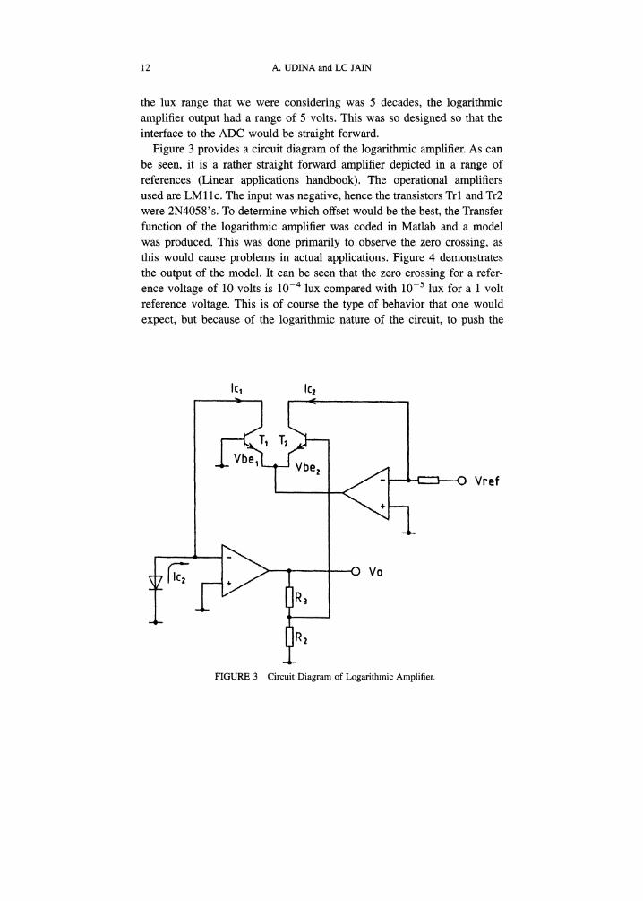
12 A. UDINA and LC JAIN
the lux range that we were considering was 5 decades, the logarithmicamplifier output had a range of 5 volts. This was so designed so that theinterface to the ADC would be straight forward.
Figure 3 provides a circuit diagram of the logarithmic amplifier. As canbe seen, it is a rather straight forward amplifier depicted in a range ofreferences (Linear applications handbook). The operational amplifiersused are LM11c. The input was negative, hence the transistors Trl and Tr2were 2N4058’ s. To determine which offset would be the best, the Transferfunction of the logarithmic amplifier was coded in Matlab and a modelwas produced. This was done primarily to observe the zero crossing, asthis would cause problems in actual applications. Figure 4 demonstratesthe output of the model. It can be seen that the zero crossing for a refer-ence voltage of 10 volts is 10-4 lux compared with 10-5 lux for a 1 voltreference voltage. This is of course the type of behavior that one wouldexpect, but because of the logarithmic nature of the circuit, to push the
[1::
OVo
FIGURE 3 Circuit Diagram of Logarithmic Amplifier.
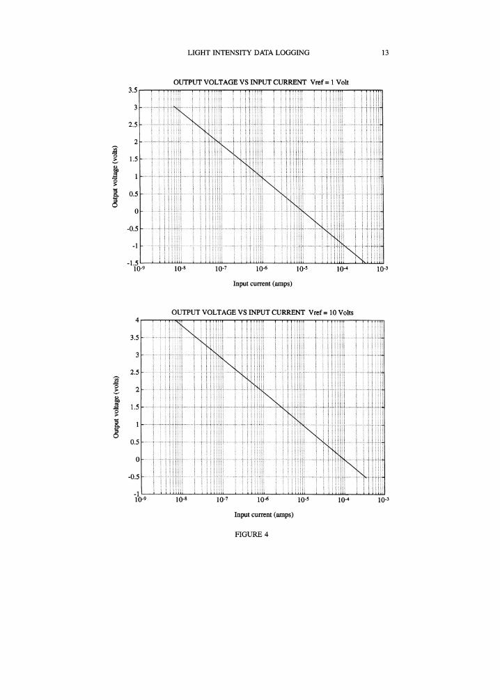
LIGHT INTENSITY DATA LOGGING 13
3.5
2.5
1.5
0.5
-0.5
OUTPUT VOLTAGE VS INPUT CURRENT Vref Volt
10-8 10-7 10-6 10-5 10-4 10-3
Input current (amps)
3.5
2.5
1.5
0.5
-0.5
-110-9 10-8
OUTPUT VOLTAGE VS INPUT CURRENT Vref= 10 Volts
!i!ili !!ilii !ii!!i
10-7 10-6 10-5 10.4 10-3
Input current (amps)
FIGURE 4

14 A. UDINA and LC JAIN
zero crossing to 10-3 lux would necessitate a reference voltage of 100volts, which was not possible, hence it was decided to maintain a referencevoltage of 10 volts.
DERIVATION OF Vo AS A FUNCTION OF IC2
It is clear from the circuit diagram in Figure 3 that
-V1 + Vbe 2 Vbe l =0 (1)
Now let us find
/cl
Also
Icl VrefR1
(2)
Thus we obtain
Icl VrefIc2 Ic2 * R1
(3)
We have from the Ebers-Moll equation that
.Vbe 1)Icl Isc * exp (,Vt
and
Ic2 Isc *,Vbe 1
exp[Vt
*NOTE* Take transistors to be the same
So substitute into (2) to obtain

LIGHT INTENSITY DATA LOGGING 15
/cllsc
,Vbe 2)* exptVt
Isc,Vbe 1
* exptVt
This gives
Icl ,Vbe 2) Vbe 1.Ic2
expt g *exp(-gt
So get
IclexpIc-- [t Vbe 2 Vbe 1)] (4)
From (1) we have that
Vbe 2- Vbe l V1
So substituting this into (4) we get
Icl V1/- exp(--) (5)
Now let us substitute (5) into (3) to get
Ic2 * R1 exp(-tTaking the log of both sides gives us
V1 Vref- ntlc2 ,R1
or
V1 Ic2 * R1- -ln(Vref
(6)
16 A. UDINA and LC JAIN
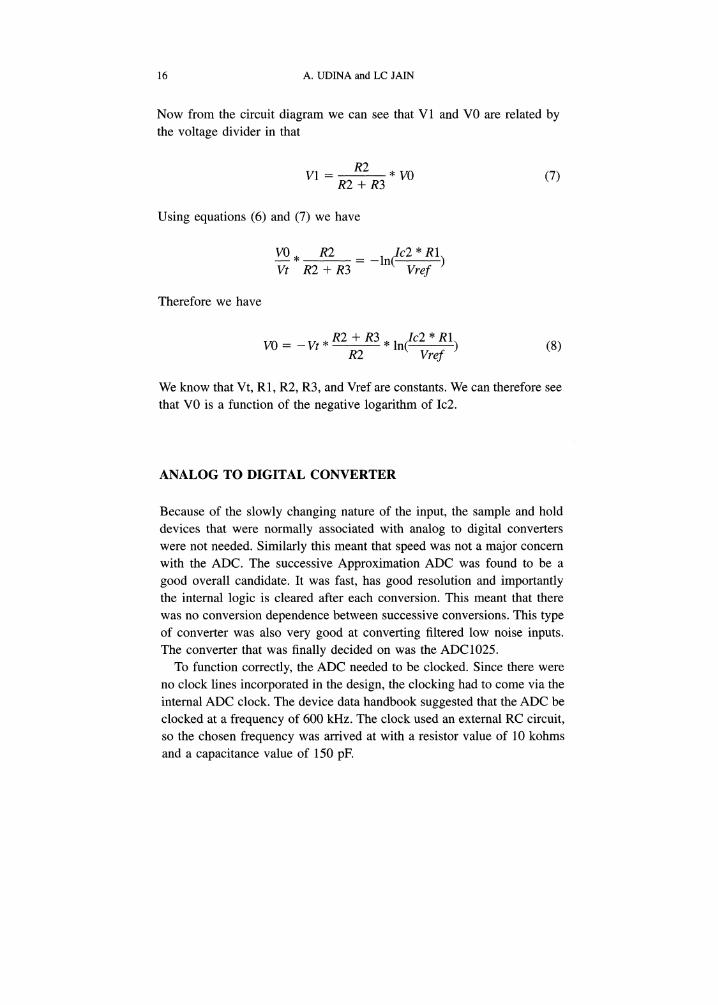
Now from the circuit diagram we can see that V1 and V0 are related bythe voltage divider in that
R2V1 * V0 (7)
R2 + R3
Using equations (6) and (7) we have
Ic2 *R1V0, R2=-In( Vrefvt R2 + R3
Therefore we have
VO -Vt *R2 + R3, Ic2 * R1)
R2ln(
Vref(8)
We know that Vt, R1, R2, R3, and Vref are constants. We can therefore seethat V0 is a function of the negative logarithm of Ic2.
ANALOG TO DIGITAL CONVERTER
Because of the slowly changing nature of the input, the sample and holddevices that were normally associated with analog to digital converterswere not needed. Similarly this meant that speed was not a major concernwith the ADC. The successive Approximation ADC was found to be a
good overall candidate. It was fast, has good resolution and importantlythe internal logic is cleared after each conversion. This meant that therewas no conversion dependence between successive conversions. This typeof converter was also very good at converting filtered low noise inputs.The converter that was finally decided on was the ADC1025.To function correctly, the ADC needed to be clocked. Since there were
no clock lines incorporated in the design, the clocking had to come via theinternal ADC clock. The device data handbook suggested that the ADC beclocked at a frequency of 600 kHz. The clock used an external RC circuit,so the chosen frequency was arrived at with a resistor value of 10 kohmsand a capacitance value of 150 pE

LIGHT INTENSITY DATA LOGGING 17
The ADC also needed a reference voltage to define the voltage spanover which it would quantize its input. In our case, the voltage span was 5volts. This was achieved by tying the reference line to the 5 volt supplyrail. This obviated the need to have the supply rails regulated so thatamplitude changes would be kept to a minimum. Testing demonstratedthat the supply rails were adequate as a reference line.
FEEDING DATA TO THE COMPUTER
The interface to the computer was through the LPT or printer port. Now,because of the configuration of the printer port, it could only accept a 4 bit
parallel stream. Hence, this meant that the data needed to be broken upinto two 4 bit words and one 2 bit word. This was achieved with the use ofthree LS125 buffers. The ten ADC outputs were divided into two sets of 4bit words, each feeding into separate buffers and one 2 bit word feedinginto the third buffer. The microprocessor then cycled through the buffersreading the 10 bits in the following sequential manner. It first enabled thehigh nibble, then the middle nibble, and finally the last two significant bits.
In this way the 10 bits were sent through 4 lines, which were then recon-structed in the computer memory.
CONCLUSION
This paper presents the design of a data logger system to measure lightintensity in the duct of skylights. The design is simple, inexpensive, andhas the capability of measuring intensity ranging from 10 lux to 105 luxwithout having to resort to range changing resistors.
Acknowledgment
We would like to thank Kim Kemeny and KimAhn Loung for their workin the production and testing of the components and devices.

International Journal of
AerospaceEngineeringHindawi Publishing Corporationhttp://www.hindawi.com Volume 2010
RoboticsJournal of
Hindawi Publishing Corporationhttp://www.hindawi.com Volume 2014
Hindawi Publishing Corporationhttp://www.hindawi.com Volume 2014
Active and Passive Electronic Components
Control Scienceand Engineering
Journal of
Hindawi Publishing Corporationhttp://www.hindawi.com Volume 2014
International Journal of
RotatingMachinery
Hindawi Publishing Corporationhttp://www.hindawi.com Volume 2014
Hindawi Publishing Corporation http://www.hindawi.com
Journal ofEngineeringVolume 2014
Submit your manuscripts athttp://www.hindawi.com
VLSI Design
Hindawi Publishing Corporationhttp://www.hindawi.com Volume 2014
Hindawi Publishing Corporationhttp://www.hindawi.com Volume 2014
Shock and Vibration
Hindawi Publishing Corporationhttp://www.hindawi.com Volume 2014
Civil EngineeringAdvances in
Acoustics and VibrationAdvances in
Hindawi Publishing Corporationhttp://www.hindawi.com Volume 2014
Hindawi Publishing Corporationhttp://www.hindawi.com Volume 2014
Electrical and Computer Engineering
Journal of
Advances inOptoElectronics
Hindawi Publishing Corporation http://www.hindawi.com
Volume 2014
The Scientific World JournalHindawi Publishing Corporation http://www.hindawi.com Volume 2014
SensorsJournal of
Hindawi Publishing Corporationhttp://www.hindawi.com Volume 2014
Modelling & Simulation in EngineeringHindawi Publishing Corporation http://www.hindawi.com Volume 2014
Hindawi Publishing Corporationhttp://www.hindawi.com Volume 2014
Chemical EngineeringInternational Journal of Antennas and
Propagation
International Journal of
Hindawi Publishing Corporationhttp://www.hindawi.com Volume 2014
Hindawi Publishing Corporationhttp://www.hindawi.com Volume 2014
Navigation and Observation
International Journal of
Hindawi Publishing Corporationhttp://www.hindawi.com Volume 2014
DistributedSensor Networks
International Journal of