
Silicon Implementation of SHA-3 Final Round Candidates ...
8
Silicon Implementation of SHA-3 Final Round Candidates: BLAKE, Grøstl, JH, Keccak and Skein Xu Guo , Meeta Srivastav , Sinan Huang , Leyla Nazhandali and Patrick Schaumont Center for Embedded Systems for Critical Applications (CESCA) Bradley Department of Electrical and Computer Engineering, Virginia Tech, Blacksburg, VA 24061 Email: {xuguo, meeta, shuang86, leyla, schaum}@vt.edu Abstract—Hardware implementation quality is an important factor in selecting the NIST SHA-3 competition finalists. However, a comprehensive methodology to benchmark five final round SHA-3 candidates in ASIC is challenging. Many factors need to be considered, including application scenarios, target technologies and optimization goals. This work describes detailed steps in the silicon implementation of a SHA-3 ASIC. The plan of ASIC prototyping with all the SHA-3 finalists, as an integral part of our SHA-3 ASIC evaluation project, is motivated by our previously proposed methodology, which defines a consistent and systematic approach to move a SHA-3 hardware benchmark process from FPGA prototyping to ASIC implementation. We have designed the remaining five SHA-3 candidates in 0.13 μm IBM process using standard-cell CMOS technology. The fabricated chip is due from foundry in May 2011. In this submission, we discuss our proposed methodology for SHA-3 ASIC evaluation and report the latest results based on pre-silicon post-layout simulation of the five SHA-3 finalists with Round 3 tweaks. I. I NTRODUCTION The SHA-3 competition organized by NIST aims to select, in three phases, a successor for the mainstream SHA-2 hash algorithms in use today. By the completion of Phase II in December 2010, 5 out of the 14 Round 2 candidates were identified for further evaluation as SHA-3 finalists. For the final round of the competition, NIST is looking for additional cryptanalytic results, as well as for performance evaluation data on hardware platforms. eBACS is a well known benchmarking environment, includ- ing a scripting environment and a performance database, for the evaluation of crypto-software [3]. Compared to such a benchmarking environment, benchmarking crypto-hardware is ad-hoc. There are several reasons why the same progress is not seen in the hardware design community. This is due, in part, to the large heterogeneity of the hardware design space, to the absence of standard metrics for cost and performance, and to the absence of standard interfaces. To address the above issues we designed a SHA-3 ASIC by following a fair SHA-3 hardware evaluation methodology. We started by defining a standard interface, and optimized the designs with a single metric in mind, Throughput-per- Area. Next, we developed an FPGA prototype that can provide a seamless transition into ASIC implementation. Finally, we designed an ASIC chip with all the five finalists with the latest round 3 tweaks. This ASIC is the focus of this paper. II. RELATED WORK The hardware evaluation of SHA-3 candidates has started shortly after the specifications and reference software imple- mentations of 51 algorithms submitted to the contest became available. The majority of initial comparisons were limited to less than five candidates. More comprehensive efforts became feasible only after NIST’s announcement of 14 candidates qualified to the second round of the competition in July 2009. Since then, several comprehensive studies in SHA-3 ASIC implementations have been reported [18], [17], [13], [10], [11], [16], [12]. Guo et al. [10] used a consistent and systematic approach to move the SHA-3 hardware benchmark process from the FPGA prototyping by [15] to ASIC implementations based 130nm CMOS standard cell technology. Tillich et al. [17] presented the first ASIC post-synthesis results using 180nm CMOS standard cell technology with high throughput as the optimization goal and further provided post-layout re- sults [18]. Henzen et al. [13] implemented several architectures in a 90nm CMOS standard cell technology, targeting high- and moderate-speed constraints separately, and presented a complete benchmark of post-layout results. Table I compares these benchmarking efforts, and demon- strates that a comparison between different ASIC benchmarks is hard because of several reasons. First, most groups do not share the same source codes. Second, the ASIC benchmarks do not use a common hardware interface. Third, the reported metrics and optimization targets are different. III. METHODOLOGY In this section, we describe the overall design flow that combines FPGA prototyping with ASIC design, and next elaborate the efforts to automate and standardize the ASIC implementation process. A. Overview Figure 1 illustrates the hardware evaluation flow for our SHA-3 ASIC benchmarking process. We developed the reg- ister transfer level (RTL) designs for the 5 Final Round can- didates for the Round 3 tweaks. These hardware descriptions are next mapped to FPGA technology or ASIC technology. We use the same RTL descriptions for both types of design flow. Our objective is to use the FPGA as a prototyping technology for the ASIC, rather than a direct technology target. Hence,
Transcript of Silicon Implementation of SHA-3 Final Round Candidates ...
Silicon Implementation of SHA-3 Final RoundCandidates: BLAKE, Grøstl, JH, Keccak and Skein
Xu Guo , Meeta Srivastav , Sinan Huang , Leyla Nazhandali and Patrick SchaumontCenter for Embedded Systems for Critical Applications (CESCA)
Bradley Department of Electrical and Computer Engineering, Virginia Tech, Blacksburg, VA 24061Email: {xuguo, meeta, shuang86, leyla, schaum}@vt.edu
Abstract—Hardware implementation quality is an importantfactor in selecting the NIST SHA-3 competition finalists. However,a comprehensive methodology to benchmark five final roundSHA-3 candidates in ASIC is challenging. Many factors need tobe considered, including application scenarios, target technologiesand optimization goals. This work describes detailed steps inthe silicon implementation of a SHA-3 ASIC. The plan of ASICprototyping with all the SHA-3 finalists, as an integral part of ourSHA-3 ASIC evaluation project, is motivated by our previouslyproposed methodology, which defines a consistent and systematicapproach to move a SHA-3 hardware benchmark process fromFPGA prototyping to ASIC implementation. We have designedthe remaining five SHA-3 candidates in 0.13 µm IBM processusing standard-cell CMOS technology. The fabricated chip is duefrom foundry in May 2011. In this submission, we discuss ourproposed methodology for SHA-3 ASIC evaluation and reportthe latest results based on pre-silicon post-layout simulation ofthe five SHA-3 finalists with Round 3 tweaks.
I. INTRODUCTION
The SHA-3 competition organized by NIST aims to select,in three phases, a successor for the mainstream SHA-2 hashalgorithms in use today. By the completion of Phase II inDecember 2010, 5 out of the 14 Round 2 candidates wereidentified for further evaluation as SHA-3 finalists. For thefinal round of the competition, NIST is looking for additionalcryptanalytic results, as well as for performance evaluationdata on hardware platforms.
eBACS is a well known benchmarking environment, includ-ing a scripting environment and a performance database, forthe evaluation of crypto-software [3]. Compared to such abenchmarking environment, benchmarking crypto-hardware isad-hoc. There are several reasons why the same progress isnot seen in the hardware design community. This is due, inpart, to the large heterogeneity of the hardware design space,to the absence of standard metrics for cost and performance,and to the absence of standard interfaces.
To address the above issues we designed a SHA-3 ASICby following a fair SHA-3 hardware evaluation methodology.We started by defining a standard interface, and optimizedthe designs with a single metric in mind, Throughput-per-Area. Next, we developed an FPGA prototype that can providea seamless transition into ASIC implementation. Finally, wedesigned an ASIC chip with all the five finalists with the latestround 3 tweaks. This ASIC is the focus of this paper.
II. RELATED WORK
The hardware evaluation of SHA-3 candidates has startedshortly after the specifications and reference software imple-mentations of 51 algorithms submitted to the contest becameavailable. The majority of initial comparisons were limited toless than five candidates. More comprehensive efforts becamefeasible only after NIST’s announcement of 14 candidatesqualified to the second round of the competition in July 2009.Since then, several comprehensive studies in SHA-3 ASICimplementations have been reported [18], [17], [13], [10], [11],[16], [12]. Guo et al. [10] used a consistent and systematicapproach to move the SHA-3 hardware benchmark processfrom the FPGA prototyping by [15] to ASIC implementationsbased 130nm CMOS standard cell technology. Tillich et al.[17] presented the first ASIC post-synthesis results using180nm CMOS standard cell technology with high throughputas the optimization goal and further provided post-layout re-sults [18]. Henzen et al. [13] implemented several architecturesin a 90nm CMOS standard cell technology, targeting high-and moderate-speed constraints separately, and presented acomplete benchmark of post-layout results.
Table I compares these benchmarking efforts, and demon-strates that a comparison between different ASIC benchmarksis hard because of several reasons. First, most groups do notshare the same source codes. Second, the ASIC benchmarksdo not use a common hardware interface. Third, the reportedmetrics and optimization targets are different.
III. METHODOLOGY
In this section, we describe the overall design flow thatcombines FPGA prototyping with ASIC design, and nextelaborate the efforts to automate and standardize the ASICimplementation process.
A. Overview
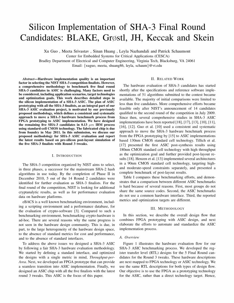
Figure 1 illustrates the hardware evaluation flow for ourSHA-3 ASIC benchmarking process. We developed the reg-ister transfer level (RTL) designs for the 5 Final Round can-didates for the Round 3 tweaks. These hardware descriptionsare next mapped to FPGA technology or ASIC technology. Weuse the same RTL descriptions for both types of design flow.Our objective is to use the FPGA as a prototyping technologyfor the ASIC, rather than a direct technology target. Hence,
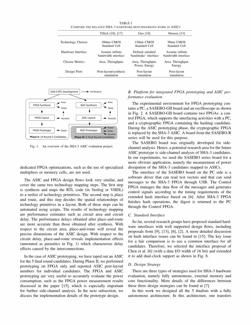
TABLE ICOMPARE THE RELATED SHA-3 HARDWARE BENCHMARKING WORK IN ASICS
Tillich [18], [17] Guo [10] Henzen [13]
Technology Choices 180nm CMOS 130nm CMOS 90nm CMOSStandard Cell Standard Cell Standard Cell
Hardware Interface Assume infinite Defined standard Assume infinitebandwidth interface ‘handshake’ interface bandwidth interface
Chosen Metrics Area, Throughput, Area, Throughput, Area, Throughput,Power, Energy Energy
Design Flow Post-layout/synthesis Post-layout Post-layoutsimulation simulation simulation
Verification
FPGA Synthesis
FPGA Layout
FPGA Prototype
ASIC Synthesis
ASIC Layout
ASIC Prototype
Area
Delay
Parasitic
Power
Area
Delay
Parasitic
Power
Delay
Phase II: 14 Round 2 Candidates Phase III: 5 Final Round Candidates
SHA-3 RTL Development
Security
Fig. 1. An overview of the SHA-3 ASIC evaluation project.
dedicated FPGA optimizations, such as the use of specializedmultipliers or memory cells, are not used.
The ASIC and FPGA design flows look very similar, andcover the same two technology mapping steps. The first stepis synthesis and maps the RTL code (in Verilog or VHDL)to a netlist of technology primitives. The second step is placeand route, and this step decides the spatial relationships oftechnology primitives in a layout. Both of these steps can beautomated using scripts. The results of technology mappingare performance estimates such as circuit area and circuitdelay. The performance delays obtained after place-and-routeare more accurate than those obtained after synthesis. Withrespect to the circuit area, place-and-route will reveal theprecise dimensions of the ASIC design. With respect to thecircuit delay, place-and-route reveals implementation effects(annotated as parasitics in Fig. 1) which characterize delayeffects caused by the interconnections.
In the case of ASIC prototyping, we have taped out an ASICfor the 5 final round candidates. During Phase II, we performedprototyping on FPGA only and reported ASIC post-layoutnumbers for individual candidates. The FPGA and ASICprototyping are very useful to accurately evaluate the powerconsumption, such as the FPGA power measurement resultsdiscussed in the paper [15], which is especially importantfor further side-channel analysis. In the next subsection, wediscuss the implementation details of the prototype design.
B. Platform for integrated FPGA prototyping and ASIC per-formance evaluation
The experimental environment for FPGA prototyping con-tains a PC, a SASEBO-GII board and an oscilloscope as shownin Fig. 2. A SASEBO-GII board contains two FPGAs: a con-trol FPGA, which supports the interfacing activities with a PC,and a cryptographic FPGA containing the hashing candidate.During the ASIC prototyping phase, the cryptographic FPGAis replaced by the SHA-3 ASIC. A board from the SASEBO-Rseries will be used for this purpose.
The SASEBO board was originally developed for side-channel analysis. Hence, a potential research area for the futureASIC prototype is side-channel analysis of SHA-3 candidates.In our experiments, we used the SASEBO series board for amore obvious application, namely the measurement of powerdissipation of the SHA-3 candidates mapped to ASICs.
The interface of the SASEBO board on the PC side is asoftware driver that can read test vectors and that can sendmessages to the SHA-3 FPGA through USB. The ControlFPGA manages the data flow of the messages and generatescontrol signals according to the timing requirements of theextended hash interface based on [6]. After SHA-3 FPGAfinishes hash operations, the digest is returned to the PCthrough the Control FPGA.
C. Standard Interface
So far, several research groups have proposed standard hard-ware interfaces with well supported design flows, includingproposals from [9], [13], [6], [2]. A more detailed discussionon hash interface issues can be found in [15]. The key issuefor a fair comparison is to use a common interface for allcandidates. Therefore, we selected the interface proposal ofChen et al. [6] (with a data I/O width of 16 bit) and extendedit to add dual-clock support as shown in Fig. 8.
D. Design Strategy
There are three types of strategies used for SHA-3 hardwareevaluation, namely fully autonomous, external memory andcore functionality. More details of the differences betweenthese three design strategies can be found at [7].
In this work we designed all the 5 finalists with a fullyautonomous architecture. In this architecture, one transfers
ControlFPGA
SHA-3FPGA/ASIC
PC
Software Driver
USB_d
USB_rxfn
USB_txen
USB_rdn
USB_wr
Slow CLK(Interface)
RESET
INIT
LOAD
FETCH
ACK
DIN
DOUT
8
16
16
SASEBO-GII Platform
StandardHashI/O
Interface
IntermediateValue Reg.
HashValueReg.
MessageReg.
Hash Core Function
EN
LOAD_MSG
BUSY
HASH_VALUE256
SHA-3 FPGA Prototype
SystemControl
SHA-3Candidate 0
SHA-3Candidate 1
SHA-3Candidate 5
InputSync
OutputSync
SHA-3 ASIC Test Chip(SASEBO-R Platform)
OscilloscopePower Measurement/Side-Channel Analysis
Fast CLK(Core Logic)
SHA-3Candidate 4
CLKManagement
Fig. 2. Experimental environment for FPGA prototyping and final ASIC testing.
message data to a hash function over multiple clock cyclesuntil a complete message block is provided. The hash modulebuffers a complete message block locally, before initiatingthe hash operation. Therefore, this architecture can workautonomously, and the resulting hash module is well suitedfor a hardware IP for system-on-chip integration.
E. Optimization Target
The use of Throughput-to-Area Ratio as the optimizationtarget for SHA-3 hardware evaluation was first proposed byGaj et al. [9], and later appeared in NIST Status Report on theSecond Round of the SHA-3 Competition as a hardware eval-uation criterion. One of the obvious advantages of choosingthis target rather than Throughput alone is that it can avoidhighly unrolled hash designs with small throughput benefitsbut significant circuit area overhead.
F. Evaluation Metrics
In this work we have used Throughput-to-Area Ratio asa primary metric and also reported other common metrics,including area, maximum frequency, maximum throughput,and power/energy efficiency.
a) Area: In this evaluation we will use the circuit area ofeach SHA-3 candidate with both the interface and hash coreafter layout. The area will be reported in kilo gate equivalents(kGE), where a gate equivalent corresponds to the area of astandard NAND2 gate in the standard cell library. We dividedthe EDA tools reported layout area with unit in µm2 by thearea of an NAND2 gate for conversion from the absolutecircuit area to kGE.
b) Throughput: In general the time required to hash amessage consists three parts: the latency for loading one blockof message, Lin , the hash core latency, Lcore, the latencyfor finalization step, Lfinal, and the latency for outputting themessage digest, Lout. For short message hashing, all these fourlatencies are important performance factors. And the metric ofLatency is frequently used to characterize the short messagehashing speed instead of Throughput. In the case of hashinga long message, Lfinal and Lout can be neglected. Since Lin
is dependent on the system I/O throughput which may vary
in different contexts, here we report the Throughput results ofthe hash core function:
Tpcore =WB × fmax
Lcore, (1)
where WB is the block size of the hash and fmax is themaximum frequency the circuit can run at.
c) Throughput-to-Area: The Throughput-to-Area Ratio isan effective metric to measure the hardware efficiency, wherethe Throughput is the above defined Tpcore and the Area isfor the layout circuit area expressed in terms of kGE.
d) Power/Energy: The power numbers are measured withfixed achievable clock frequencies based on the average powerof hashing long messages, and the capture period is only forthe core hashing operations (e.g. round function for each blockof input message). The energy metric is expressed as energyper bit of the input message block compressed by the hashcore function.
IV. VLSI IMPLEMENTATION OF SHA-3 HASH FUNCTIONS
In this section we briefly review the implementations of eachSHA-3 finalist. For details on the SHA-3 candidates pleaserefer to the related specification documents on NIST SHA-3 web sites. For hardware architectures, we have looked intoseveral public available reference implementations [1], [8], [5]and optimized them for our system architecture.
A. BLAKE
BLAKE follows a HAIFA iteration mode and operates onan inner state that can be represented as a four by four matrixof words. The inner state is initialized using an Initial Value(IV), a salt and a counter. The state is updated using the Gfunction, which is based on the ChaCha stream cipher [4].The G function mainly contains modular addition, XOR, androtate operations.
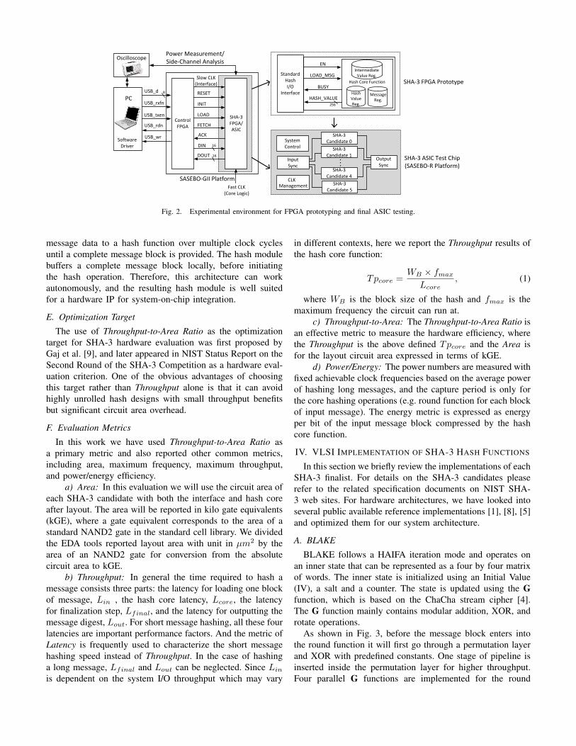
As shown in Fig. 3, before the message block enters intothe round function it will first go through a permutation layerand XOR with predefined constants. One stage of pipeline isinserted inside the permutation layer for higher throughput.Four parallel G functions are implemented for the round
Hash MSG
Permutation
G G G GState
Finalization
IV Data
Hash Value
Fig. 3. Structure of the BLAKE-256 core.
P State Q State
P Q
Hash
Data
Hash Value
IV
Fig. 4. Structure of the Grøstl-256 core.
process. Eight G functions or even fully unrolled structuresare also possible high performance solutions if there is noarea constraint. Each G function instantiates two carry-saveadders.
B. Grøstl
Grøtl is a wide-pipe Merkle-Damgard hash algorithm withan output transformation. The compression function is a novelconstruction, using two fixed 2n-bit permutations together.The output transformation processes the final chaining state,and discards half the bits of the result, yielding an n-bithash output. The underlying fixed permutations are themselvesbased closely on the structure of AES, reusing the S-box, butexpanding the size of the block to 512 bits for Grøtl-256 in astraightforward way.
Grøstl can be implemented with parallel computation ofP and Q permeations as well as a single permutation with
M State
H State
IVData
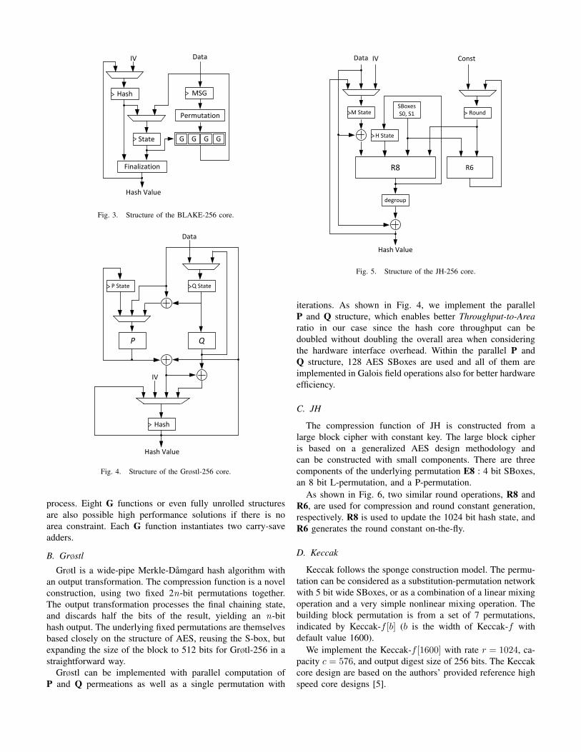
SBoxes S0, S1 Round
Const
R8 R6
degroup
Hash Value
Fig. 5. Structure of the JH-256 core.
iterations. As shown in Fig. 4, we implement the parallelP and Q structure, which enables better Throughput-to-Arearatio in our case since the hash core throughput can bedoubled without doubling the overall area when consideringthe hardware interface overhead. Within the parallel P andQ structure, 128 AES SBoxes are used and all of them areimplemented in Galois field operations also for better hardwareefficiency.
C. JH
The compression function of JH is constructed from alarge block cipher with constant key. The large block cipheris based on a generalized AES design methodology andcan be constructed with small components. There are threecomponents of the underlying permutation E8 : 4 bit SBoxes,an 8 bit L-permutation, and a P-permutation.
As shown in Fig. 6, two similar round operations, R8 andR6, are used for compression and round constant generation,respectively. R8 is used to update the 1024 bit hash state, andR6 generates the round constant on-the-fly.
D. Keccak
Keccak follows the sponge construction model. The permu-tation can be considered as a substitution-permutation networkwith 5 bit wide SBoxes, or as a combination of a linear mixingoperation and a very simple nonlinear mixing operation. Thebuilding block permutation is from a set of 7 permutations,indicated by Keccak-f [b] (b is the width of Keccak-f withdefault value 1600).
We implement the Keccak-f [1600] with rate r = 1024, ca-pacity c = 576, and output digest size of 256 bits. The Keccakcore design are based on the authors’ provided reference highspeed core designs [5].
State
Keccak-f[1600] (r=1024, c=576)
Permutation
Buffer
Data
Hash Value
Round Constant
Fig. 6. Structure of the Keccak-256 core.
Key State
Key Schedule
Hash Value
Mix andPermute
Add SubKey
Data
IV
Add SubKey
Fig. 7. Structure of the Skein512-256 core.
E. Skein
Skein is an iterative hash algorithm built on a tweakableblock cipher C Threefish. Threefish is used to build the com-pression function of Skein using a modified Mateas-Meyer-Oseas construction, which is then iterated in a chaining modesimilar to HAIFA. The designers refer to the whole construc-tion as a Unique Block Iteration (UBI) mode. Threefish isa 72-round substitution-permutation network using a 128-bitMIX function consisting of a 64-bit addition, rotate and XORoperations.
As shown in Fig. 7, we implemented the Skein512-256 ver-sion and each Threefish-512 round out of 72 rounds consistsof four parallel MIX operation and a permutation. Four roundsare unrolled and chained together in hardware.
F. Summary
Table II summarizes the major implementation aspects ofeach SHA-3 finalist. The design decisions are made to achievethe primary optimization for Throughput-to-Area.
V. ASIC REALIZATION
Compared to other published work on SHA3 chip design[13], our chip has the following benefits:
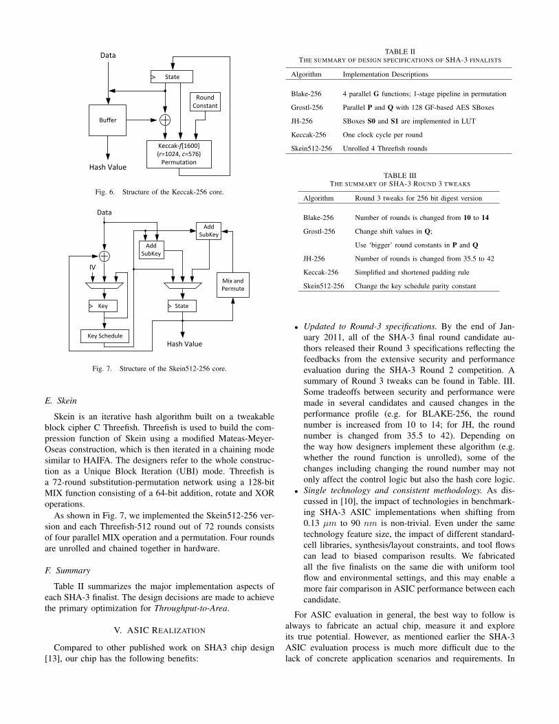
TABLE IITHE SUMMARY OF DESIGN SPECIFICATIONS OF SHA-3 FINALISTS
Algorithm Implementation Descriptions
Blake-256 4 parallel G functions; 1-stage pipeline in permutation
Grøstl-256 Parallel P and Q with 128 GF-based AES SBoxes
JH-256 SBoxes S0 and S1 are implemented in LUT
Keccak-256 One clock cycle per round
Skein512-256 Unrolled 4 Threefish rounds
TABLE IIITHE SUMMARY OF SHA-3 ROUND 3 TWEAKS
Algorithm Round 3 tweaks for 256 bit digest version
Blake-256 Number of rounds is changed from 10 to 14
Grøstl-256 Change shift values in Q;
Use ‘bigger’ round constants in P and Q
JH-256 Number of rounds is changed from 35.5 to 42
Keccak-256 Simplified and shortened padding rule
Skein512-256 Change the key schedule parity constant
• Updated to Round-3 specifications. By the end of Jan-uary 2011, all of the SHA-3 final round candidate au-thors released their Round 3 specifications reflecting thefeedbacks from the extensive security and performanceevaluation during the SHA-3 Round 2 competition. Asummary of Round 3 tweaks can be found in Table. III.Some tradeoffs between security and performance weremade in several candidates and caused changes in theperformance profile (e.g. for BLAKE-256, the roundnumber is increased from 10 to 14; for JH, the roundnumber is changed from 35.5 to 42). Depending onthe way how designers implement these algorithm (e.g.whether the round function is unrolled), some of thechanges including changing the round number may notonly affect the control logic but also the hash core logic.
• Single technology and consistent methodology. As dis-cussed in [10], the impact of technologies in benchmark-ing SHA-3 ASIC implementations when shifting from0.13 µm to 90 nm is non-trivial. Even under the sametechnology feature size, the impact of different standard-cell libraries, synthesis/layout constraints, and tool flowscan lead to biased comparison results. We fabricatedall the five finalists on the same die with uniform toolflow and environmental settings, and this may enable amore fair comparison in ASIC performance between eachcandidate.
For ASIC evaluation in general, the best way to follow isalways to fabricate an actual chip, measure it and exploreits true potential. However, as mentioned earlier the SHA-3ASIC evaluation process is much more difficult due to thelack of concrete application scenarios and requirements. In
addition, our ASIC design has constraints, too, including thearea budget, the total number of available IOs for the chipsocket on the testing platform, and the capabilities of thetesting infrastructure. In the following sections, we will discussabout how we designed the SHA-3 ASIC to tackle all theabove issues and how the final area and performance resultswill be affected by those design decisions.
A. Chip Architecture
As shown in Fig. 8, besides the SHA-3 candidates modulesour SHA-3 chip contains an on-chip clock management mod-ule, a system control module, and a synchronization module.All these features are integrated in order to fulfill the needsof fitting the SHA-3 ASIC chip into the SASEBO-R platformand meet our final chip testing requirements.
• Clock Management Module. This module has two func-tions: clock gating and clock generation. The clock gatingis used to isolate the impact of the other candidateswhen measuring the power consumption of one candidateat a time. As shown in Fig. 2, all the inputs to theSHA-3 ASIC are generated from the control FPGA onboard which connects to the SHA-3 ASIC. By defaultthe control FPGA runs at a relatively low frequency(e.g. 24 MHz). It is not recommended to transmit highfrequency signals through on board connections. For highfrequency testing purpose, we used the custom-cell designapproach to integrate a ring oscillator based voltage-controlled oscillator (VCO) into the chip together with astandard-cell implemented clock divider, which can offera good range of clock frequencies on chip. The on-chipgenerated clocks are also MUXed with the external clockinput and can be configured through dedicated ports.
• System Control Module. The system control module isin charge of decoding the control signals for algorithmselection, clock gating, clock division ratio and hashmode from ports. The SHA-3 ASIC can support operationmodes. The normal hashing mode loads 16 bit input datafor each transfer until it buffers a whole block of datato start compression. This I/O bottleneck makes it verydifficult for full speed testing since there is a relativelylong message loading period between two consecutivehashing. Therefore, we defined a second mode of opera-tion: full speed testing. Under this hash mode, the inputbuffer of each candidate only stores 16 bit of input dataper block, and replicates this input data to fill an entireblock.
• Cross-Clock Domain Synchronizer. There are two clockdomains in our chip: the slow one is for the interfacinglogic and the fast one is for hash modules. In orderto avoid complex synchronizer designs based on asyn-chronous FIFOs or feedback synchronization and allevi-ate the burden of the backend process to deal with the twoclock domains, we simplified the synchronizer design bymaking a reasonable assumption that the internal hashclock working frequency is always at least two timesfaster than the slow interface clock. As a result, the slow
Post-layout Simulation
RTL Design in Verilog
Parasitic Extraction
Logic Synthesis
Layout
stdcell lib
process lib
Post-syn Simulation
LVS/DRC
test vectors
latency throughput
die area pin count
latency throughput
Power Energy
IC Compiler
Design Compiler
StarRCXT
VCS/PrimeTime
Hercules/Assura
Design Quality
GDSII file
IBM 130nm CMR8SF-RVT Process SAGE-XTM v2.0 Standard Cell Library
VCS/PrimeTime
Fig. 9. The overview of our ASIC design flow.
interface can be deemed as a normal control signal andthe whole chip only has one single fast clock eitherinput from external clock or internal VCO generatedclock. Within this approach we extended the standardhash interface [6] of each candidate to integrate thissynchronizer, and the final reported layout area for eachcandidate will also include the overhead of this extendedhash interface.
B. Constraints
The timing constraints are selected to optimize Throughput-to-Area Ratio, using the methodology described in [11]. Basedon this analysis, we categorized the five SHA-3 candidatesplus the SHA256 based on their achievable frequencies afterlayout into three groups: 250 MHz (JH and Keccak), 200 MHz(Grøstl and SHA256), and 125 MHz (BLAKE and Skein).
With these timing constraints for each group of hash mod-ules, we are able to finish the layout of the SHA-3 ASIC withthe chip core of 1.656 mm × 1.656 mm and overall chip areafitting in the die size of 5 mm2 including pad cells.
C. Design Environment
We used the Synopsys Design Compiler (C-2009.06-SP3) tomap the SHA-3 RTL codes to IBM MOSIS 0.13 µm CMOSTechnology with CMR8SF-RVT standard cell library. We usethe typical case condition characterization of the standardcell libraries. The 130nm technology uses 7 metal layers. Ingeneral, more metal layers allow for a denser interconnect,and hence a more optimal use of die area.
The Synopsys IC Compiler (C-2009.06-SP5) is used for theback-end process. The overall chip core area utilization ratioafter layout is 73%. The utilization is defined as the die areadevoted to active components (standard cells) as compared tothe total die area. After place-and-route, design flow errorssuch as timing and Design Rule Check (DRC) violations mayoccur. In some cases, the initial utilization must be lowered inorder to relax the constraints to the place-and-route process.
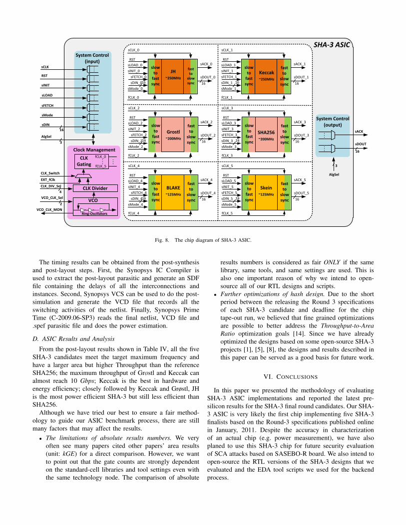
sCLK
RST
sLOAD
sFETCH
sDIN
sINIT
EXT_fClk
AlgSel
sMode
fCLK_0CLK Gating
AlgSel
sACK
sDOUT
System Control(input)
fCLK_5
Ring-Oscillators
CLK Divider
VCO
CLK_Switch
VCO_CLK_Sel
CLK_DIV_Sel
4
2
3
16
sCLK_0
RST
sLOAD_0
sFETCH_0
sACK_0
sDIN_0
sDOUT_0
sINIT_0
sMode_0
16 16
slowto
fastsync
fastto
slowsync
JH~250MHz
fCLK_0
sCLK_1
RST
sLOAD_1
sFETCH_1
sACK_1
sDIN_1
sDOUT_1
sINIT_1
sMode_1
16 16
slowto
fastsync
fastto
slowsync
fCLK_1
sCLK_2
RST
sLOAD_2
sFETCH_2
sACK_2
sDIN_2
sDOUT_2
sINIT_2
sMode_2
16 16
slowto
fastsync
fastto
slowsync
fCLK_2
sCLK_3
RST
sLOAD_3
sFETCH_3
sACK_3
sDIN_3
sDOUT_3
sINIT_3
sMode_3
16 16
slowto
fastsync
fastto
slowsync
fCLK_3
sCLK_4
RST
sLOAD_4
sFETCH_4
sACK_4
sDIN_4
sDOUT_4
sINIT_4
sMode_4
16 16
slowto
fastsync
fastto
slowsync
fCLK_4
sCLK_5
RST
sLOAD_5
sFETCH_5
sACK_5
sDIN_5
sDOUT_5
sINIT_5
sMode_5
16 16
slowto
fastsync
fastto
slowsync
fCLK_5
Keccak~250MHz
Grostl~200MHz
SHA256~200MHz
BLAKE~125MHz
Skein~125MHz
System Control(output)
16
3
SHA-3 ASIC
VCO_CLK_MON
Clock Management
Fig. 8. The chip diagram of SHA-3 ASIC.
The timing results can be obtained from the post-synthesisand post-layout steps. First, the Synopsys IC Compiler isused to extract the post-layout parasitic and generate an SDFfile containing the delays of all the interconnections andinstances. Second, Synopsys VCS can be used to do the post-simulation and generate the VCD file that records all theswitching activities of the netlist. Finally, Synopsys PrimeTime (C-2009.06-SP3) reads the final netlist, VCD file and.spef parasitic file and does the power estimation.
D. ASIC Results and Analysis
From the post-layout results shown in Table IV, all the fiveSHA-3 candidates meet the target maximum frequency andhave a larger area but higher Throughput than the referenceSHA256; the maximum throughput of Grøstl and Keccak canalmost reach 10 Gbps; Keccak is the best in hardware andenergy efficiency; closely followed by Keccak and Grøstl, JHis the most power efficient SHA-3 but still less efficient thanSHA256.
Although we have tried our best to ensure a fair method-ology to guide our ASIC benchmark process, there are stillmany factors that may affect the results.
• The limitations of absolute results numbers. We veryoften see many papers cited other papers’ area results(unit: kGE) for a direct comparison. However, we wantto point out that the gate counts are strongly dependenton the standard-cell libraries and tool settings even withthe same technology node. The comparison of absolute
results numbers is considered as fair ONLY if the samelibrary, same tools, and same settings are used. This isalso one important reason of why we intend to open-source all of our RTL designs and scripts.
• Further optimizations of hash design. Due to the shortperiod between the releasing the Round 3 specificationsof each SHA-3 candidate and deadline for the chiptape-out run, we believed that fine grained optimizationsare possible to better address the Throughput-to-AreaRatio optimization goals [14]. Since we have alreadyoptimized the designs based on some open-source SHA-3projects [1], [5], [8], the designs and results described inthis paper can be served as a good basis for future work.
VI. CONCLUSIONS
In this paper we presented the methodology of evaluatingSHA-3 ASIC implementations and reported the latest pre-silicon results for the SHA-3 final round candidates. Our SHA-3 ASIC is very likely the first chip implementing five SHA-3finalists based on the Round-3 specifications published onlinein January, 2011. Despite the accuracy in characterizationof an actual chip (e.g. power measurement), we have alsoplaned to use this SHA-3 chip for future security evaluationof SCA attacks based on SASEBO-R board. We also intend toopen-source the RTL versions of the SHA-3 designs that weevaluated and the EDA tool scripts we used for the backendprocess.

TABLE IVASIC CHARACTERIZATION OF THE SHA-3 ASIC CHIP IN IBM MOSIS 0.13 µm CMOS TECHNOLOGY WITH CMR8SF-RVT STANDARD CELL
LIBRARY, THE GATE EQUIVALENT COUNT IS CALCULATED BY DIVIDING THE POST-LAYOUT DIE AREA BY THE AREA OF A NAND2XLTF (5.76 µm2)
Block Size Core Latency Area Max Freq. Throughput Throughput-to-Area Power Energy[bits] [cycles] [kGEs] [MHz] [Gbps] [kbps/GE] [mW] [mJ/Gbits]
BLAKE-256 512 30 34.15 125 2.13 62.47 17.83 41.78Grøstl-256 512 11 124.34 200 9.31 74.87 101.38 87.12JH-256 512 42 49.29 250 3.05 61.83 12.50 41.02Keccak-256 1024 24 42.49 250 10.67 251.05 17.83 16.71Skein512-256 512 21 66.36 125 3.05 45.93 41.75 68.50
SHA256 512 68 21.67 200 1.51 69.54 5.95 31.62
*: NIST SHA-3 Round 3 Specifications by January, 2011.**: The above numbers are from post-layout simulation with slow chip interface clock at 10MHz and fast hash core clock at 25MHz.***: Throughput, Power, and Energy numbers are measured for hash core operations.
1
SHA3 ASIC Chip
Blake
Groestl
JH
Keccak
Skein
SHA256
Fig. 10. Die layout of the SHA-3 ASIC chip in 0.13 µm IBM process usingstandard cell CMOS technology.
REFERENCES
[1] AIST-RCIS. SHA-3 hardware project, March 2011. http://www.rcis.aist.go.jp/special/SASEBO/SHA3-en.html.
[2] Brian Baldwin, Neil Hanley, Mark Hamilton, Liang Lu, Andrew Byrne,Maire ONeill, and William P. Marnane. FPGA Implementations ofthe Round Two SHA-3 Candidates. In The Second SHA-3 CandidateConference, August 2010.
[3] D. Bernstein and T. Lange. eBACS: ECRYPT Benchmarking ofCryptographic Systems, March 2011. http://bench.cr.yp.to.
[4] D. J. Bernstein. ChaCha, a variant of Salsa20, January 2008. http://cr.yp.to/chacha/chacha-20080128.pdf.
[5] Guido Bertoni, Joan Daemen, Michael Peeters, and Gilles Van Assche.The Keccak sponge function family – Updated VHDL package, March2011. http://keccak.noekeon.org/VHDL 3.0.html.
[6] Zhimin Chen, Sergey Morozov, and Patrick Schaumont. A HardwareInterface for Hashing Algorithms. Cryptology ePrint Archive, Report2008/529, 2008. http://eprint.iacr.org/2008/529.
[7] ECRYPT. The SHA-3 Zoo, March 2011. http://ehash.iaik.tugraz.at/wiki/SHA-3 Hardware Implementations.
[8] Omitted for blind review.[9] Kris Gaj, Ekawat Homsirikamol, and Marcin Rogawski. Fair and
Comprehensive Methodology for Comparing Hardware Performance ofFourteen Round Two SHA-3 Candidates Using FPGAs. In Stefan Man-gard and Francois-Xavier Standaert, editors, Cryptographic Hardwareand Embedded Systems, CHES 2010, volume 6225 of Lecture Notes inComputer Science, pages 264–278. Springer Berlin / Heidelberg, 2010.
[10] Xu Guo, Sinan Huang, Leyla Nazhandali, and Patrick Schaumont. Fairand Comprehensive Performance Evaluation of 14 Second Round SHA-3 ASIC Implementations. In The Second SHA-3 Candidate Conference,August 2010.
[11] Xu Guo, Sinan Huang, Leyla Nazhandali, and Patrick Schaumont. OnThe Impact of Target Technology in SHA-3 Hardware Benchmark
Rankings. Cryptology ePrint Archive, Report 2010/536, 2010. http://eprint.iacr.org/2010/536.
[12] L. Henzen, J.-P. Aumasson, W. Meier, and R. C.-W. Phan. VLSICharacterization of the Cryptographic Hash Function BLAKE. VeryLarge Scale Integration (VLSI) Systems, IEEE Transactions on, 2010.
[13] Luca Henzen, Pietro Gendotti, Patrice Guillet, Enrico Pargaetzi, MartinZoller, and Frank Gurkaynak. Developing a Hardware EvaluationMethod for SHA-3 Candidates. In Stefan Mangard and Francois-XavierStandaert, editors, Cryptographic Hardware and Embedded Systems,CHES 2010, volume 6225 of Lecture Notes in Computer Science, pages248–263. Springer Berlin / Heidelberg, 2010.
[14] Ekawat Homsirikamol, Marcin Rogawski, and Kris Gaj. Comparinghardware performance of fourteen round two sha-3 candidates usingfpgas. Cryptology ePrint Archive, Report 2010/445, 2010. http://eprint.iacr.org/.
[15] K. Kobayashi, J. Ikegami, M. Knezevic, E.X. Guo, S. Matsuo, SinanHuang, L. Nazhandali, U. Kocabas, Junfeng Fan, A. Satoh, I. Ver-bauwhede, K. Sakiyama, and K. Ohta. Prototyping platform forperformance evaluation of SHA-3 candidates. In Hardware-OrientedSecurity and Trust (HOST), 2010 IEEE International Symposium on,pages 60 –63, 2010.
[16] A.H. Namin and M.A. Hasan. Hardware implementation of the com-pression function for selected SHA-3 candidates. CACR 2009-28, July2009.
[17] Stefan Tillich, Martin Feldhofer, Mario Kirschbaum, Thomas Plos,Jorn-Marc Schmidt, and Alexander Szekely. High-Speed HardwareImplementations of BLAKE, Blue Midnight Wish, CubeHash, ECHO,Fugue, Grøstl, Hamsi, JH, Keccak, Luffa, Shabal, SHAvite-3, SIMD,and Skein. Cryptology ePrint Archive, Report 2009/510, 2009. http://eprint.iacr.org/2009/510.
[18] Stefan Tillich, Martin Feldhofer, Mario Kirschbaum, Thomas Plos, Jorn-Marc Schmidt, and Alexander Szekely. Uniform Evaluation of HardwareImplementations of the Round-Two SHA-3 Candidates. In The SecondSHA-3 Candidate Conference, August 2010.