
Signal-, Power-Integrity, & EMI Update - Ansys · PDF fileSignal-, Power-Integrity, & EMI...
37
© 2011 ANSYS, Inc. September 14, 2011 1 Signal-, Power- Integrity, & EMI Update Bill McGinn Senior Application Engineer
-
Upload
truongnhan -
Category
Documents
-
view
301 -
download
11
Transcript of Signal-, Power-Integrity, & EMI Update - Ansys · PDF fileSignal-, Power-Integrity, & EMI...

© 2011 ANSYS, Inc. September 14, 2011
1
Signal-, Power-Integrity, & EMI Update
Bill McGinn
Senior Application Engineer

© 2011 ANSYS, Inc. September 14, 2011
2
• ANSYS ECAD Solutions
• HFSS for Signal Integrity
• SIwave Full BRD and PKG Solutions
• SI Circuit Simulation for IBIS-AMI and Memory
• Q3D Extractor 11.0 Updates
Overview

© 2011 ANSYS, Inc. September 14, 2011
3
ANSYS ECAD Solutions

© 2011 ANSYS, Inc. September 14, 2011
4
AnsoftLinks Translation Paths
Cadence Mentor ODB++ Zuken
Q3D SIwave HFSS Designer TPA Icepak Mechanical
AnsoftLinks
HFSS PlanarEM
Solver on Demand
Static ECAD Transfer (.anf)
AnsoftLinks with Extracta
Dynamic ECAD Transfer
Cadence
Virtuoso SiP APD Allegro
Altium
Nexxim HSPICE

© 2011 ANSYS, Inc. September 14, 2011
5
HFSS for Signal Integrity
ECAD & Field Solver Improvements

© 2011 ANSYS, Inc. September 14, 2011
6
Solver on Demand: An ECAD Interface for HFSS
Problem Description:
1. Converting package and printed circuit board layout data to 3D mechanical CAD models creates a large amount of unnecessary overhead in the geometry database
2. A key capability needed for wide-spread use of HFSS as an extraction tool is to make it accessible to non experts
Solution:
1. When HFSS is used for package and PCB extraction a 2D Electrical CAD layout editor is better suited for model creation and setup
2. The Designer Layout editor with Solver on Demand improves HFSS accessibility for non-expert engineers who need to use HFSS for package and PCB extraction
– It provides an EMI solution for 2 layer pkg and board design with HFSS and PlanarEM
3. The Designer Layout editor with Solver on Demand significantly reduces the engineering time required to set up package and pcb models for extraction with HFSS
4. Cadence design flows allows a user to solve with HFSS from within the Cadence environment using Cadence Extracta and an IPC link

© 2011 ANSYS, Inc. September 14, 2011
7
“HFSS for ECAD”
Two Design Flows for Electrical Design
• Mechanical CAD
– Connectors, Waveguides
– HFSS
• Electric CAD (layout)
– PCBs, Packages, On-chip Passives
– HFSS - Solver on Demand

© 2011 ANSYS, Inc. September 14, 2011
8
HFSS Setup & Solve Within Cadence SPB
• Dynamic ECAD Flow
• Create and Solve models with HFSS from within Cadence Allegro, APD, & SiP
HFSS Solution Progress

© 2011 ANSYS, Inc. September 14, 2011
9
HFSS Setup & Solve Within Virtuoso
• Setup & Solve • Lumped ports - Horizontal & Vertical
• Layer Stack Up Simplified • Automated Via Clustering • Back Annotation of Touchstone Results
© 2011 ANSYS, Inc. September 14, 2011
10
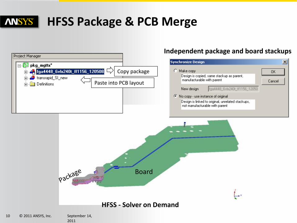
HFSS Package & PCB Merge
Copy package
Paste into PCB layout
Independent package and board stackups
Board
HFSS - Solver on Demand
© 2011 ANSYS, Inc. September 14, 2011
11
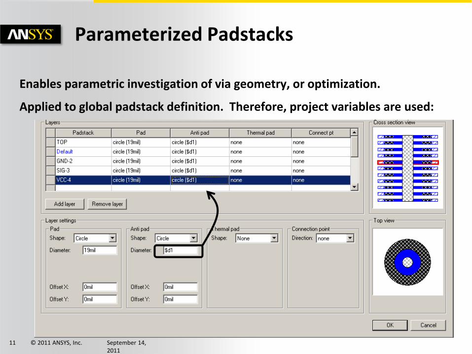
Parameterized Padstacks
Enables parametric investigation of via geometry, or optimization.
Applied to global padstack definition. Therefore, project variables are used:

© 2011 ANSYS, Inc. September 14, 2011
12
Parameterized Differential Vias

© 2011 ANSYS, Inc. September 14, 2011
13
HFSS Port Assignment by Pad
Select pad -> RT Click -> Create Port
Port name is derived from pad name

© 2011 ANSYS, Inc. September 14, 2011
14
HFSS ECAD Layout Editor
• Tag differential nets for s-parameter postprocessing.
– Turn net visibility on/off.

© 2011 ANSYS, Inc. September 14, 2011
15
Huray Surface Roughness: Modeled vs. Measured
Nodule Radius; a = 0.5 um
Hall-Huray Surface Ratio: low = 1, mid = 3, high = 6
Surface Roughness Reference: P.G. Huray, O. Oluwafemi, J. Loyer, E. Bogatin, and X. Ye; "Impact of Copper Surface Texture on Loss: A Model That Works", DesignCon 2010, February 1 - 4, 2010.
Resonance Reference: P. Pathmanathan, C.M. Jones, S.G. Pytel, D.L. Edgar, P.G. Huray, “Power Loss due to Periodic Structures in High-Speed Packages and Printed Circuit Boards”, European Microelectronics Packaging Conference – IMAPS 2011, Brighton, England, September 12 – 15, 2011

© 2011 ANSYS, Inc. September 14, 2011
16
HFSS ECAD Layout Editor
Parameterizable Etch Factor
Parameterizable Surface Roughness
Automatic Causal Djordjevic Sarkar Dielectric Models

© 2011 ANSYS, Inc. September 14, 2011
17
Passivity Enforcement: Interpolating Sweeps
Additional criteria to determine convergence
Passivity violations used as new basis points
Improves reliability of models in transient SPICE simulations

© 2011 ANSYS, Inc. September 14, 2011
18
Lump Port De-embedding (Calibration)
Physical dimensions of lump port carries current
• “intrinsic inductance”
Analytic inductance is de-embedded from port S-parameters
“Calibrating” the “test fixture” of the measurement
Implementation analogous to wave port de-embedding

© 2011 ANSYS, Inc. September 14, 2011
19
HFSS ECAD – Causal Sweep Option
Option to fit an interpolation sweep with causal basis functions
Very efficient fitting and guarantees causal S-parameters
ANSYS Causality Checker - 1.8 % error without causal enforcement - 0.0 % error with causal enforcement

© 2011 ANSYS, Inc. September 14, 2011
20
HFSS for the SI Community Summary New in R14
• Parameterized padstacks
• Automated causal material
• Multi-frequency point adapting
• Integrated 2D/3D views
• Huray Surface Roughness Models
• Lumped Port De-embedding
• Trapezoidal Trace Cross-sections
• Automated Virtuoso HFSS Design
• Passivity Enforced Interpolation
• HFSS Solves from within Cadence
HFSS Padstack Editor with Parameterization

© 2011 ANSYS, Inc. September 14, 2011
21
Show Nets in HFSS for MCAD
“Show Nets” identifies 3D conducting paths between terminals

© 2011 ANSYS, Inc. September 14, 2011
22
SIwave Full BRD and PKG Solutions
DDR3 and High Speed Serial Improvements

© 2011 ANSYS, Inc. September 14, 2011
23
Signal Net Analyzer • Ideal and non-ideal lumped parameters (i.e Zo) • Nexxim and HSPICE RLC simulations
Via to Via Coupling • Differential pair accuracy improvements
Solver Support for Arbitrary Antipad Cutouts • Improvement in via modeling accuracy
SYZ Solver Improvements • Guaranteed passive/causal SYZ solutions
FWS Improvements for Large Port Count Devices • Faster convergence and reduced RAM when using “Iterated
Fitting of Passivity” for large port count devices
Improved “Push Excitation” Accuracy & Robustness • SIwave now forces required interpolation from Designer 7.0.
Improved Surface Roughness • Added Huray surface roughness model
PI Advisor Improvements • Genetic Algorithm supports weighting of constraints • Genetic Algorithm supports new constraints
– Maximum Total Capacitor Area – Maximum Number of Capacitor Types
Improved SYZ Storage Architecture • 6x reduction in disk space for SYZ parameters
Solver
Memory and High Speed Serial Improvements
64 bit GUI for Windows
Table Impedance Calculator • Flight time plots • Transient Simulations with Nexxim or HSPICE
PKG & PCB Automation • Graphical selection & merging
Pin Grouping Automation • Multi-part select with group per part/net definitions
Improved Validation Checker • Detection of pins belonging to multiple pin groups
Automated DCIR Reports
Equipotential Pads for DCIR Solver
Temperature Profile Plotting from Icepak
Improved Surface Roughness • Addition of Huray model in GUI
PI Advisor Improvements • Allowance of weighting constraints in GUI • Additional constraints added
– Maximum Total Capacitor Area – Maximum Number of Capacitor Types
Improved ODB++ Support
Support for X2Y Low Inductance Capacitors
GUI

© 2011 ANSYS, Inc. September 14, 2011
24
DDR3 Solutions: Signal Net Analyzer
• Displays Z0, length, time delay, and reference layer
• All possible paths (from each pin to every other pin on net) are displayed
– Sorted in descending order of path distance
• User can click on an individual path in the table
– Variation in Z0 is graphically displayed
– Path is highlighted in SIwave’s main layout window
• Ideal reference layer mode (default)
– Traces on top & bottom metal layers are assumed to be microstrips
– Interior traces are assumed to be striplines
• Non-ideal reference layer mode
– Reference layer is explicitly calculated for each trace segment
– Some traces may be floating (no suitable reference layer available)

© 2011 ANSYS, Inc. September 14, 2011
25
Automated DCIR Reporting
Click Here

© 2011 ANSYS, Inc. September 14, 2011
26
SI Circuit Simulation for High Speed Serial and Memory Applications

© 2011 ANSYS, Inc. September 14, 2011
27
Macro-Modeling Functionality
Circuit Simulation • Designer • Simplorer • Other
• State-space fitting • Passivity enforcement • Passivity checker • S-parameter visualization • S-matrix reduction • Macro-model generation
HFSS
SIwave
Q3D
Network Data Explorer
Designer
• State Space • Simplorer • Spectre • HSPICE • PSPICE
Measured Data
New functionality for the SI market

© 2011 ANSYS, Inc. September 14, 2011
28
Macro-Modeling with Network Data Explorer
Touchstone Models from Arbitrary Source can be converted to Multiple Model Types with Causality and Passivity Enforcement!
Advanced features
New!

© 2011 ANSYS, Inc. September 14, 2011
29
ANSYS Library & Design Kit Support
Design Engineers require accurate electrical models for components when designing circuits
A key feature of the web based library support is ease of use. Library installation generally requires users to download files, uncompress them and place them in the correct location on a local drive.
Automated web based download from within Designer automates these steps, making it easy for users to keep their component libraries up to date.
Design Kits
• DDR3, PCIe 3.0, HDMI , SATA, SAS, …
Scripting Libraries
• FWS commands, Footprinting, Reporting Templates, …

© 2011 ANSYS, Inc. September 14, 2011
30
High Speed Serial Design with IBIS-AMI
• Automated IBIS-AMI Importing
– IBIS-AMI Specification Testing
• Pass/Fail
• Advanced

© 2011 ANSYS, Inc. September 14, 2011
31
User Defined Transmit Jitter for HSS Design
PDF vs. time defined in a text file
No jitter
Contents of text file userdefined.txt

© 2011 ANSYS, Inc. September 14, 2011
32
Q3D Extractor 11.0

© 2011 ANSYS, Inc. September 14, 2011
33
Q3D Extractor Overview
Major Applications • 64 Bit Windows GUI
• Magnetic Materials
• Terminal Setup Improvements for AC RL Solver
• Touch Panel Expression Caching for CG and RL
• Selectable Frequency Export for Lumped SPICE Passives
• DCRL Speed Up
• CG Convergence improvements
• HPC Improvements
– Network Installs
– Fixed Variables
• Greatly improves post processing speed for projects with large numbers of variables – i.e. Via Wizard
• 3D Modeling Enhancements
• WB Integration Improvements for DSO & Optimetrics
© 2011 ANSYS, Inc. September 14, 2011
34
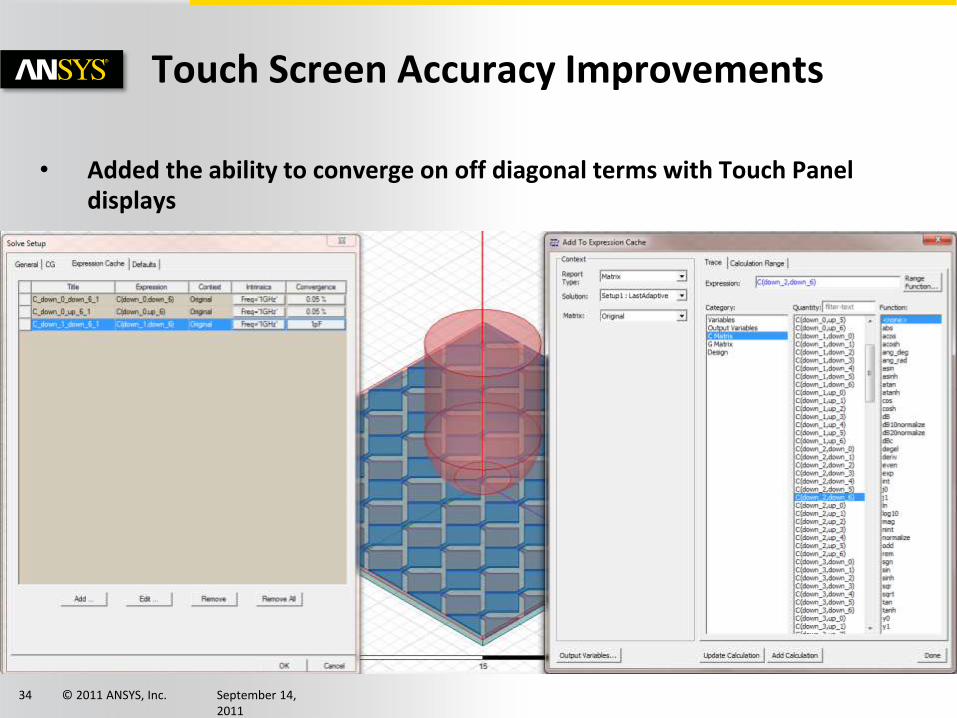
Touch Screen Accuracy Improvements
• Added the ability to converge on off diagonal terms with Touch Panel displays

© 2011 ANSYS, Inc. September 14, 2011
35
0.00 0.01 0.10 1.00 10.00 100.00Freq [MHz]
25.00
30.00
35.00
40.00
45.00
50.00
55.00
AC
L(C
oil:C
oil_
in,C
oil:C
oil_
in)
[nH
]
Q3DDesign2XY Plot 1 ANSOFT
Curve Info
ACL(Coil:Coil_in,Coil:Coil_in)Setup1 : Sw eep2
Q3D – Magnetic Materials
Q3D AC 10 s Maxwell 3D 50 min
Q3D DC 6min 30 s
Sweep 2 s
Total < 7 min 50 min
Peak RAM 0.6 GB 5 GB
L(f)
Simulation Time
HFSS
Maxwell*
Q3D
* Each additional frequency point takes ~ 15 minutes to solve with Maxwell
Electroplated Nickel has 5
Bulk Nickel has 600

© 2011 ANSYS, Inc. September 14, 2011
36
3D Modeler Enhancements
View customization.
• Z-stretch.
• 64-bit user interface

© 2011 ANSYS, Inc. September 14, 2011
37
• ANSYS ECAD Solutions
• HFSS for Signal Integrity
• SIwave Full BRD and PKG Solutions
• SI Circuit Simulation for IBIS-AMI and Memory
• Q3D Extractor 11.0 Updates
Summary