SIGNAL INTEGRITY:PCB & INTERCONNECT TEST “FOCUS ON ...
35
Eric Oseassen – Application Engineer 4/16/2020 [email protected] SIGNAL INTEGRITY:PCB & INTERCONNECT TEST “FOCUS ON DEEMBEDDING”
Transcript of SIGNAL INTEGRITY:PCB & INTERCONNECT TEST “FOCUS ON ...

Eric Oseassen – Application Engineer4/16/[email protected]
SIGNAL INTEGRITY:PCB & INTERCONNECT TEST“FOCUS ON DEEMBEDDING”

Rohde & Schwarz
SYLLABUS
Signal Integrity: PCB and Interconnect Test2 20.04.2021
PART 1: PCB AND INTERCONNECT TEST CHALLENGES• CHANNEL IMPAIRMENTS
• SURVEY OF BANDWIDTH REQUIREMENTS
PART 2: DEEMBEDDING - HIGH-SPEED DIGITAL AND RF APPLICATIONS• BRIEF OVERVIEW OF SCATTERING PARAMETERS
• DEEMBEDDING TYPES
PART 3: DEEMBEDDING: COMMON USE CASES• FIVE TYPES OF DEEMBEDDING
• EZD (EAZY DEEMBEDDING) - (K210) IMPLEMENTATION AND RESULTS
PART 4: PCB AND INTERCONNECT: SIGNAL INTEGRITY TESTS• MODEL CHANNEL IMPAIRMENT WITH CORRECTED DATA
• SUMMARY & CONCLUSION

PART1 - PCB AND INTERCONNECT TEST CHALLENGES

Rohde & Schwarz
HIGH-SPEED DIGITAL DESIGN: TX – CHANNEL – RX
Signal Integrity: PCB and Interconnect Test4
Transmitter Channel Receiver
Scopes VNAs ScopesBERTs / AWGs
20.04.2021
Measurements:
- Return Loss, Insertion Loss- Mode Conversion, Skew- Crosstalk- Impedance over time- Eye Diagram

Rohde & Schwarz
CHALLENGES FOR PCBS AND INTERCONNECTSIN HIGH-SPEED DIGITAL DESIGNS► impedance mismatches - discontinuities at
packages, vias, connectors
20.04.2021 Signal Integrity: PCB and Interconnect Test5
Source: PCI-SIG Developers Conference 2019; PCIe®5.0 Electrical Update
Example: PCIe 5.0discontinuities on signal path between Root Complex and End Point
Example: PCIe 5.0total loss budget: 36 dB @ 16GHz

Rohde & Schwarz
CHALLENGES FOR PCBS AND INTERCONNECTSIN HIGH-SPEED DIGITAL DESIGNS► impedance mismatches - discontinuities at
packages, vias, connectors, interposers► losses and frequency response of PCB
material− for 112 Gbps and above:
PCB signal traces will be by-passed by cables
► crosstalk: NEXT, FEXT
20.04.2021 Signal Integrity: PCB and Interconnect Test6
Transmission
Transmission
Tx Rx
Tx Rx
Rx Tx
Transmission
NEXT
victim
aggressor
aggressor

Rohde & Schwarz
CHALLENGES FOR PCBS AND INTERCONNECTSIN HIGH-SPEED DIGITAL DESIGNS► Physical Structures
• impedance mismatches - discontinuities at packages, VIA’s, connectors
• losses and frequency response of PCB material• crosstalk: NEXT, FEXT• multiple resonant structures, e.g. via stubs
(backdrill), fiber weave effects, etc.• Manufacturing Issues
20.04.2021 Signal Integrity: PCB and Interconnect Test7
Backdrill

Rohde & Schwarz
HIGH-SPEED DIGITAL DESIGN: PCIENETWORK INFRASTRUCTURE, DATA CENTERS, …
8 20.04.2021 Signal Integrity: PCB and Interconnect Test
PCIe Spec. Raw
Bandwidth
(per Lane)
Data Rate
(Total)
NRZ / PAM VNA
BW requirement
SOC test
VNA
BW requirement
(PCBs, Interconnects)
…
Gen 3 8.0Gbps 8.0GT/s NRZ
Gen 4 16.0Gbps 16.0GT/s NRZ 25GHz 20GHz(system performance)
Gen 5 32.0Gbps 32.0GT/s NRZ 50GHz 40GHz(system performance)
Gen 6 64.0Gbps 64.0GT/s PAM4 50GHz(spec. in progress)
40GHz(spec. in progress)
Note:ı GT/s = Gtransfers / secı Gbps = Gbit / sec

Rohde & Schwarz
HIGH-SPEED DIGITAL DESIGN: IEEE802.3NETWORK INFRASTRUCTURE, DATA CENTERS, …
9 20.04.2021 Signal Integrity: PCB and Interconnect Test
IEEE Spec. Copper Cables Backplanes Signalling
Bandwidth
(per Lane)
NRZ / PAM VNA
BW requirement
(PCBs, Interconnects)
… … … …
802.3by802.3bj
25GBASE-CR100GBASE-CR4
25GBASE-KR100GBASE-KR4
25Gbps NRZ 25GHz
802.3cd 50GBASE-CR1100GBASE-CR2200GBASE-CR4
50GBASE-KR1100GBASE-KR2200GBASE-KR4
50Gbps PAM4 26.56GHz
802.3ck 100GBASE-CR1200GBASE-CR2400GBASE-CR4
100GBASE-KR1200GBASE-KR2400GBASE-KR4
100Gbps PAM4 50GHz(spec. in progress)
PART 2: DEEMBEDDING:HIGH-SPEED DIGITAL AND RF APPLCATIONS

Rohde & Schwarz
TYPICAL PCB MEASUREMENTS IN DIGITAL SYSTEMSS-PARAMETER BASICS
Signal Integrity: PCB and Interconnect Test
test fixture
Port 1
Port 3
Port 2
Port 4
DUTa
b
DUTa
b
Principle:1.) The VNA measures a differential 2-port device as single-ended 4-port device
Logical Port 1
Logical Port 2
=
b1b2b3b4
a1a2a3a4
S11 S12 S13 S14S21 S22 S23 S24S31 S32 S33 S34S41 S42 S43 S44
20.04.202111

Rohde & Schwarz
TYPICAL PCB MEASUREMENTS IN DIGITAL SYSTEMSS-PARAMETER BASICS
Signal Integrity: PCB and Interconnect Test
test fixture
Port 1
Port 3
Port 2
Port 4
DUTa
b
DUTa
b
Principle:2.) The VNA calculates mixed mode S-Parameters out of measured single ended S-Parameters
Logical Port 1
Logical Port 2
Port 1 Port 1Port 2 Port 2
Differential-Mode
stimulus
Common-Mode
stimulus
Differential-
mode
Response
Port 1
Port 2
Port 1
Port 2
Common-
mode
Response
dd11 dd12 dc11 dc12
dd21 dd22 dc21 dc22
cd11 cd12 cc11 cc12
cd21 cd22 cc21 cc22
S S S S
S S S S
S S S S
S S S S
.
Naming Convention: S mode res., mode stim., port res., port stim.
20.04.202112

Rohde & Schwarz
EXPLORE DE-EMBEDDING
13 20.04.2021 Signal Integrity: PCB and Interconnect Test

Rohde & Schwarz
Fixture
FOUR TIERS OF DE-EMBEDDING
14 20.04.2021 Signal Integrity: PCB and Interconnect Test
Port Extension
Direct Compensation
Fixture Calibration
De-Embedding
open, short, or both
Fixture
open, short, or both
Fixture
Cal standards
DUT
Fixture
DUT
Fixture
Right Left

Rohde & Schwarz
PORT EXTENSION (PORT OFFSET)
20.04.2021 Signal Integrity: PCB and Interconnect Test15
► Assume text fixture is perfectly matched and behaves like a ideal transmission line− Defined delay− Defined loss
► Delay and loss can be − Manually entered by the user − Automatically determined
► Standard feature on most VNAs► Easy configuration, but limited accuracy
− Real world effects such as reflections, crosstalk, etc. are not well represented

Rohde & Schwarz
DIRECT COMPENSATION
20.04.2021 Signal Integrity: PCB and Interconnect Test16
► Doesn’t assume that the fixture behaves like ideal transmission line
► Measures frequency dependent transmission characteristics of fixture− Fixture terminated with open, short, or both− Best results when open and short are used
► Like port extension, only works well at lower frequencies (several GHz and below)
► Enforces Passivity► Displays a “DOT” on Smith Chart

Rohde & Schwarz
FIXTURE CALIBRATION
20.04.2021 Signal Integrity: PCB and Interconnect Test17
► Directly characterize the fixture► Full calibration at DUT connection point
− Moves the calibration plane to the DUT− “Calibrate out” the fixture
► More accurate solution► Requires characterized calibration standards
− Usually quite difficult to implement

Rohde & Schwarz
TRL (THROUGH, REFLECT, LINE)
20.04.2021 Signal Integrity: PCB and Interconnect Test18
► Directly characterize the fixture► Full calibration at DUT connection point
− Moves the calibration plane to the DUT− “Calibrate out” the fixture
► More accurate solution► Requires characterized calibration standards
− Challenging to implement well
Thru Line 1
Line 2
Line 3
Reflect

Rohde & Schwarz
ALGORITHMIC BASED DE-EMBEDDING
20.04.2021 Signal Integrity: PCB and Interconnect Test19
► Directly characterize the fixture► Full calibration at DUT connection point
− Moves the calibration plane to the DUT− “Calibrate out” the fixture
► More accurate solution► Requires defined calibration standard
− Less difficult to implement
PART 3: DEEMBEDDING:COMMON USE CASES

Rohde & Schwarz
USE CASE #1: RF DEVICES WITHOUT COAXIAL CONNECTORSCHARACTERIZATION + MEASUREMENT WITH VNA
Lead-in / lead-out characterization with VNA:step 1: calibration with coaxial standards
(→ calibration plane)step 2: characterization and deembedding
of lead-in and lead-out(→ reference plane at DUT)
all VNA measurements at new reference plane
20.04.2021 Signal Integrity: PCB and Interconnect Test21
Device under Test
lead-in lead-out
Calibration Plane
Fixture
2x Thru
lead-ins
DUT

Rohde & Schwarz
USE CASE #2: SOC INTERFACE TEST W. DEEMBEDDINGCHARACTERIZATION WITH VNA, MEASUREMENT WITH SCOPE
Lead-in / lead-out characterization with VNA:step 1: calibration with coaxial standards
(→ calibration plane)step 2: characterization of lead-in and extrapolation to DC step 3: import to oscilloscope for deembedding
(→ reference plane at ball)all scope measurements at new measurement plane (ball of SoC: System on Chip)
20.04.2021 Signal Integrity: PCB and Interconnect Test22
balls
bumps
Silicon Package under Test
Calibration Planelead-in
DieSubstrate

Rohde & Schwarz
USE CASE #3: CABLE TEST WITH DEEMBEDDINGCHARACTERIZATION + MEASUREMENT WITH VNA
Lead-in / lead-out characterization with VNA:step 1: calibration with coaxial standards
(→ calibration plane)step 2: characterization and deembedding
of lead-in and lead-out(→ reference plane at cable)
all VNA measurements at new reference plane
20.04.2021 Signal Integrity: PCB and Interconnect Test23
Cable under Test
lead-in lead-out
Calibration Plane Calibration Plane
Fixture Fixture

Rohde & Schwarz
USE CASE #4: PCB TEST WITH DEEMBEDDINGCHARACTERIZATION + MEASUREMENT WITH VNA
Signal Integrity: PCB and Interconnect Test24
Lead-in / lead-out characterization with VNA:step 1: calibration with coaxial standards
(→ calibration plane)step 2: characterization and deembedding
of lead-in and lead-out(→ reference plane at area of interest)
all VNA measurements at new reference plane
automatic calibration unite.g. R&S ZN-Z54
Typical electronic or manual calibration moves the reference plane to point A
Accurate measurement needs to move to reference plane B
A A
B B
20.04.2021
lead-in lead-out
area ofinterest
example: via test
Rohde & Schwarz
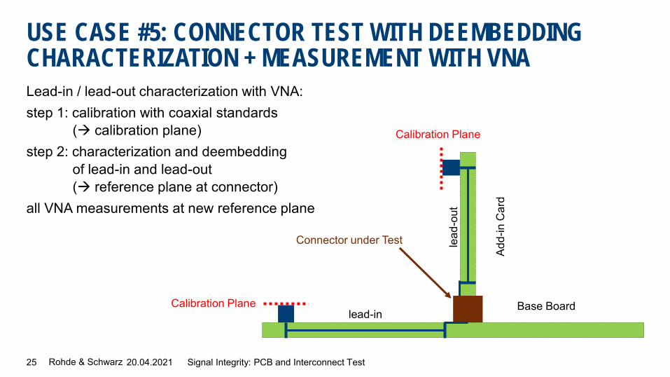
USE CASE #5: CONNECTOR TEST WITH DEEMBEDDINGCHARACTERIZATION + MEASUREMENT WITH VNA
Lead-in / lead-out characterization with VNA:step 1: calibration with coaxial standards
(→ calibration plane)step 2: characterization and deembedding
of lead-in and lead-out(→ reference plane at connector)
all VNA measurements at new reference plane
20.04.2021 Signal Integrity: PCB and Interconnect Test25
Base Board
Add-
in C
ard
lead-in
lead
-out
Calibration Plane
Calibration Plane
Connector under Test

Rohde & Schwarz
DEEMBEDDING OF LEAD-IN / LEAD-OUT TRACES
Deembedding Method Integrated into R&S ZNA / R&S ZNB:► EZD: Eazy Deembedding (ZNx-K210)
Deembedding Coupons:► 2x Thru standard
20.04.2021 Signal Integrity: PCB and Interconnect Test26
Fixture
Lead-in traces Lead-out traces
DUTDUT
Test Coupon
Slide
18

Rohde & Schwarz
LAB IMPLEMENTATION
20.04.2021 Signal Integrity: PCB and Interconnect Test27
RESULTS OF EZD
“ZNx-K210”

Rohde & Schwarz
MEASUREMENT OF PCIE GEN5 SMT - HYPERION BOARD
28 20.04.2021 Signal Integrity: PCB and Interconnect Test
Daughter
Card

Rohde & Schwarz
Implementation in R&S ZNA, R&S ZNB / ZNBT:1: Load or measure 2 x Thru 2: Measure DUT + Test Fixture 3: Run Tool
29
GENERAL REQUIREMENT:DEEMBEDDING OF LEAD-IN / LEAD-OUT TRACES
20.04.2021 Signal Integrity: PCB and Interconnect Test

Rohde & Schwarz
PCIe Gen5 SMT with Hyperion Board
30
BEFORE & AFTER EZD DE-EMBEDDING
20.04.2021 Signal Integrity: PCB and Interconnect Test
• More than 3dB of insertion loss is recovered using the EZD tool
• Return Loss is “tamed” with the high frequency magnitude ripple mitigated.

PART 4: PCB AND INTERCONNECT: SIGNAL INTEGRITY TESTS

Rohde & Schwarz
TYPICAL PCB MEASUREMENTS IN DIGITAL SYSTEMSEXAMPLE: EYE DIAGRAM
Signal Integrity: PCB and Interconnect Test
Measured DUT RF Channel
Simulated Ideal PRBS15 signal
Add Jitter Add Amplitude Noise Output Eye response from DUT
Equalised Eye response
TX RX
20.04.202132

Rohde & Schwarz
TYPICAL PCB MEASUREMENTS IN DIGITAL SYSTEMSEYE DIAGRAM
Define pass/fail areas to ensure a proper eye opening
Signal Integrity: PCB and Interconnect Test20.04.202133

Frequency Domain VNA:► return loss, insertion loss► mode conversion► crosstalk: NEXT, FEXT► derived values, e.g.: COM / ERL
Channel Operating Margin Effective Return Loss
► De-Embed Lead-In and
Lead-Out Structures
► Model Channel Impairments • Convolve Serial Data with
Frequency Domain Data
SUMMARYR&S ZNA
R&S ZNB
R&S ZNBT

CONCLUSION
❖ A TECHNIQUE WAS DESCRIBED WHICH UTILIZES A VNA AND THE EZD (P370) UTILITY TO
REMOVE OR DEEMBED THE EFFECTS OF FIXTURES UPON A DATA CHANNEL
❖ THIS TECHNIQUE REQUIRES ONLY A 2X THRU
❖ SUBSEQUENTLY, CHANNEL MODELING CAN BE EXPLORED USING TRUE DUT BEHAVIOR