SGTL5000, Low Power Stereo Codec with Headphone Amp - Data ...

SGTL5000 Evaluation Platform
User’s Guide
v2.0.0

SGTL5000 Evaluation Platform
1. SCOPE .......................................................................................................................................32. GETTING STARTED ..................................................................................................................4
2.1. Software Installation ...........................................................................................................................42.2. USB Driver Installation .......................................................................................................................4
3. BOARD SETUP PROCEDURE .................................................................................................93.1. Jumper Options ..................................................................................................................................93.2. Board Connections ............................................................................................................................93.3. Example Setup .................................................................................................................................10
4. HARDWARE ............................................................................................................................114.1. Evaluation Board Features ..............................................................................................................114.2. Evaluation Board Layout ..................................................................................................................114.3. Power linear regulators ....................................................................................................................12
5. SOFTWARE .............................................................................................................................135.1. Initialization ......................................................................................................................................135.2. Routing .............................................................................................................................................145.3. I2S ....................................................................................................................................................155.4. Inputs ...............................................................................................................................................165.5. Outputs ............................................................................................................................................175.6. Digital Audio Processing (DAP) .......................................................................................................18
5.6.1. DAP Mixer ..........................................................................................................................185.6.2. SGTL5000 Surround ..........................................................................................................185.6.3. SGTL5000 Bass Enhance ..................................................................................................185.6.4. PEQ/GEQ/Tone Control .....................................................................................................185.6.5. AVC ....................................................................................................................................19
5.7. Direct Register Access .....................................................................................................................19
2 Freescale Semiconductor Inc.

SGTL5000 Evaluation Platform
1. SCOPEThe evaluation platform is designed to allow the user to test the features and perfor-mance of the SGTL5000 audio codec. The evaluation board can be used as ademo or development platform.
SGTL5000 is an audio codec that utilizes two analog inputs (LINEIN and MIC IN),two analog outputs (LINEOUT and HPOUT), one digital input (I2S IN) and one digi-tal output (I2S OUT). Communication to the chip is performed through either I2C orSPI. SGTL5000 comes in 2 packages: 3x3mm 20-pin QFN, and 5x5mm 32-pinQFN. The information in this document applies to both packages.
Freescale Semiconductor Inc. 3

SGTL5000 Evaluation Platform
2. GETTING STARTED
2.1. Software Installation• Copy the following from the CD to any location on your hard drive:
• StereoCodecControlSoftware.exe• FTC Drivers folder
• Copy SGTL5000_CA1_Init_Script.txt from the CD to C:\ drive (directly to C:).
2.2. USB Driver Installation• Make sure that the evaluation board jumpers are configured correctly (refer to
section 3.1). The jumpers are pre-configured before shipping so that the board is ready to be used.
• Connect the USB cable from the PC to the board.• Connect the 5V power supply to the board and turn on the board.
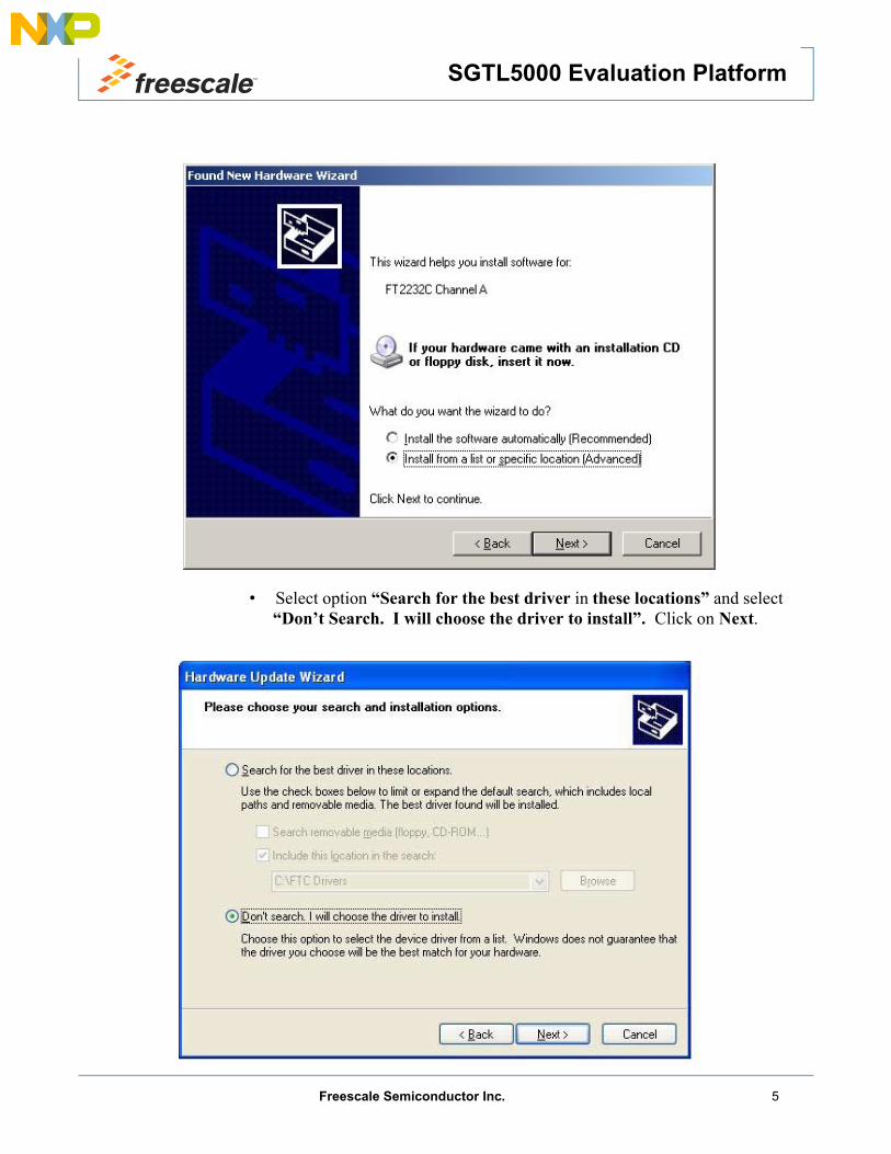
• Windows will detect the new device and automatically launch the “Add Hardware Wizard”
• Select option “Install from a list or Specific Location (Advanced)”and click Next.
4 Freescale Semiconductor Inc.
SGTL5000 Evaluation Platform
• Select option “Search for the best driver in these locations” and select “Don’t Search. I will choose the driver to install”. Click on Next.
Freescale Semiconductor Inc. 5

SGTL5000 Evaluation Platform
• Select “Universal Serial Bus Controllers” from the list.
• Select on “Have Disk”.
6 Freescale Semiconductor Inc.

SGTL5000 Evaluation Platform
• Browse to “FTC Drivers” folder unzipped from the SGTV58XXControl.zip and select “ftd2xxx.inf” file. Click “Open”.Click “Next” in the next window.
• Windows will now detect the device FT2232C Channel A. Windows logo testing window will pop-up. Click Continue Anyway.
Freescale Semiconductor Inc. 7

SGTL5000 Evaluation Platform
• FT2232C Channel B will be detected next. Windows logo testing window will pop-up. Click Continue Anyway.
• Now your eval board is ready to be used.
8 Freescale Semiconductor Inc.

SGTL5000 Evaluation Platform
3. BOARD SETUP PROCEDURE
3.1. Jumper OptionsSGTL5000 Evaluation Board provides users with various stuffing options in order touse different features of the board.
• External power (JP3, JP4, JP5): Jumper pins 1, 2 to use external voltagesource using banana plugs for each rail. Jumper pins 2, 3 to use internal regula-tors• MCLK Source (JP2): Jumper pins 1, 4 to use onboard oscillator. Jumperpins 2, 5 to use external MCLK via SMB connector (J10). Jumper pins 3, 6 touse MCLK provided by an Audio Precision PSIA via I2S Headre (J2)• MIC select (JP1): Jumper pins 1, 2 for onboard microphone (X1). Jumperpins 2, 3 to use microphone jack (J6)
3.2. Board ConnectionsThe following connection may be used as a guide.
SGTL5000Audio out
AP HeadersUSB to PC
5V
VDDD
VDDA
VDDIO
GND
Audio in
MCLK
SGTL5000 Evaluation Board connection Diagram
Freescale Semiconductor Inc. 9

SGTL5000 Evaluation Platform
3.3. Example Setup• Connect power and input/outputs according to the aforementioned connections
jumper settings and connection diagram• Open Audio Precision software
• Set up digital i/o for PSIA, and configure for I2S frame clock and bit clock output, and MCLK out
• Open SGTL5000 control software• Select I2C connection type, hit Connect• Select 256*Fs, 48kHz, Slave mode. Hit initialize• Configure an I2S input to DAC and I2S outputs• Select Program Route• Unmute DAC output
• Perform any necessary testing
10 Freescale Semiconductor Inc.

SGTL5000 Evaluation Platform
4. HARDWARE
4.1. Evaluation Board Features• SGTL5000 Audio Codec• LINEIN RCA analog input jack• LINEOUT RCA analog output jack• Selectable mini-jack or onboard microphone input• Stereo headphone mini-jack analog output, with optional capless design cir
cuitry• Two-row headers for buffered I2S digital input/output• Support for onboard or external MCLK source• USB to I2C/SPI communication port• 5V input voltage through either internal LDO regulators, or external individual
supplies
4.2. Evaluation Board LayoutThe following shows the physical layout and placement of components of theSGTL5000 evaluation board. (Please note that the picture shown below is forSGTL5000 32QFN evaluation board. SGTL5000 20QFN evaluation board is blue incolor. The information in this document applies to both SGTL5000 packages)
Figure 1. SGTL5000 Evaluation Board with Components Identified
Freescale Semiconductor Inc. 11

SGTL5000 Evaluation Platform
• Inputs include one RCA connector for LINEIN, and one mono microphone input 3.5mm mini-jack for external MIC. The board also has anan be either 3.5mm mini-jack or on-board microphone.
• Outputs include one RCA connector for LINEOUT, and one stereo 3.5mm mini-jack for HP OUT.
• AP I2S headers are a 2x8 pin array for Audio Precision PSIA connectors. These headers are provided to connect Audio Precision’s frame clk, bit clk, mas-ter clk and data to the chip.
• USB jack to connect the board to the PC via a USB cable. The software sends commands to the board via USB and the FTDI chip on the board converts it to I2C/SPI to talk to the chip. The FTDI chip is powered by the USB and a green LED indicates that.
• 5V power is a 2.1mm positive-center connector for the 5V wall-wart supply pro-vided with the kit. When the power switch is turned on, a blue LED indicates that the board is powered on.
• Individual external power can be supplied to the board via either bare wires, or banana-type connectors
• MCLK is supplied via I2S header, onboard oscillator, or SMB connector.
4.3. Power linear regulatorsIf only a 5V board power supply is connected, the supplies for VDDD, VDDA, andVDDIO must be switched to use the onboard regulators. These regulators are Ana-log Devices ADP1712AUJZ.By default, the regulator outputs are as follows:
The output for each regulator is determined by the formulaVOUT = 0.8 V (1 + R1/R2)where: R1 is the resistor from OUT to ADJ.R2 is the resistor from ADJ to GND.
)V( egatloV tuptuOliaR rewoP8.1DDDV8.1ADDV3.3OIDDV
Table 1. Linear regulator output voltages
12 Freescale Semiconductor Inc.

SGTL5000 Evaluation Platform
5. SOFTWAREThe SGTL5000 Control Software allows a user access to all of the features withinSGTL5000.
5.1. Initialization
• From the Initialization tab, the user selects the communication protocol to inter-face with the SGTL5000 chip - I2C or Ethernet. Click ‘Connect’ to connect to the board.
• Click on ‘Chip Initialize’. This will power up the analog and digital blocks, setup the default clocks (as shown in the clocks section of the Initialization page), and unmute the ADC and outputs.
• Clock configuration can be done on this page as well. The ‘Chip Initialize’ already sets it up in the default state. So additional configuraiton is required unless the parameters need to be changed. From the SYS_MCLK menu, PLL can be chosen if needed. If used, the PLL must be powered up by direct write under Direct Register Access page and the INT_DIVISOR/FRAC_DIVISOR divi-sors need to be programmed correctly. Please refer to the datasheet on how to
Freescale Semiconductor Inc. 13

SGTL5000 Evaluation Platform
configure the PLL. Please note that the divisors must be calculated based on the external MCLK rate.
5.2. Routing
From the Routing page, various signal paths are set from input to output.• Inputs include: LINEIN, MIC, I2S_DIN• LINEIN or MICIN may be configured through the ADC or directly pass-through
to HP_OUT.• Outputs include: LINEOUT, Headphone (HP), I2S_DOUT• Routes may or may not include the use of the Digital Audio Processor (DAP).
Please note that when DAP is routed, it must also be enabled under the Digital Audio Processor page. Otherwise, no audio will pass through DAP.
Routes may also be edited once programmed. To do so, select the route that is tobe edited, press the "Edit Route" button, make the route changes, and select "Pro-gram Route."
14 Freescale Semiconductor Inc.

SGTL5000 Evaluation Platform
5.3. I2S
From the I2S tab, specifics to the digital I2S communication are programmed. TheSCLK frequency, word length, and data alignment are options that are programma-ble.
Freescale Semiconductor Inc. 15

SGTL5000 Evaluation Platform
5.4. Inputs
• The input screen has the volume and gain controls for the two analog inputs - Line In and Microphone.
• The software configures the left and right volume together to the same value. When ‘Independent L/R Volume Control’ is checked, left and right volumes can be controlled indepndently. The left and right channels also have independent mutes.
• The microphone has two sliders for Gain and Bias, the latter is dependent on on-board settings of the Mic Bias circuitry.
16 Freescale Semiconductor Inc.
SGTL5000 Evaluation Platform
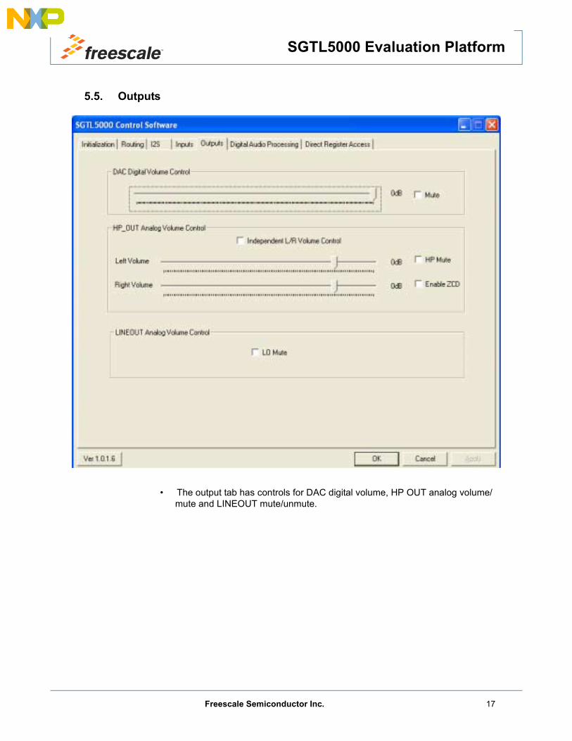
5.5. Outputs
• The output tab has controls for DAC digital volume, HP OUT analog volume/mute and LINEOUT mute/unmute.
Freescale Semiconductor Inc. 17

SGTL5000 Evaluation Platform
5.6. Digital Audio Processing (DAP)
5.6.1. DAP MixerThe DAP Mixer allows a second audio signal to be mixed in with the main audiostream. Both can be mixed as a percentage of total signal. The Mixer can be con-figured to route from the ADC or I2S_DIN.
5.6.2. SGTL5000 SurroundSGTL5000 Surround widens the soundscape, and has width settings from 1-7, forvarying amounts of processing.
5.6.3. SGTL5000Bass EnhanceSGTL5000 Bass Enhance boosts bass levels. Programmable settings include the lowpass filter cutoff frequency, high pass filter cutoff frequency, Bass Level, Left/Rightlevel, and a multiplier that can dramatically increase the effect.
5.6.4. PEQ/GEQ/Tone ControlSGTL5000 includes a 7-band parametric equalizer (PEQ) that can be programmedthrough the software's presets. Custom PEQ curves can be created, as well.The 5-band graphic equalizer (GEQ) is fully programmable, with bands of 115Hz,330Hz, 990Hz, 3000Hz, and 9900Hz. Each can be adjusted up to +/-12dB.
SGTL5000 SurroundDAP Mixer SGTL5000 Bass PEQ/GEQ Tone Control AWC
18 Freescale Semiconductor Inc.

SGTL5000 Evaluation Platform
Tone Control allows the user to adjust the Bass and Treble levels, up to +/-12dB.
5.6.5. AVCThe Automatic Volume Control (AVC) helps prevent clipping or speaker damage byallowing the user to set a threshold from which SGTL5000 will attenuate or gain thesignal to reach the specified value. Attack and decay rates are fully programmable.
5.7. Direct Register Access
• From the Direct Register Access tab, users can read and write directly to regis-ters without the use of the GUI.
• The Register Write Monitor shows all read and written-to registers from the cur-rent session. Scripts can be saved and run from here as well.
• Support for SPI register writes is on this tab.
Freescale Semiconductor Inc. 19

5
5
4
4
3
3
2
2
1
1
D D
C C
B B
A A
Headphone
Analog Outputs PG.5
Master/Slave
Communication PG.6
MCLKSource
I2C ADR0Select
USB to I2C/SPI I2S Signals PG.7
Analog Inputs PG.4
SGTL5000PG. 3
I2S0 Interface
Line-In / Microphone
I2C/SPIMode Select
Block Diagram
Lineout
AP PSIAHEADER
DigitalHeader
Power PG. 8
External5VDC in
ExternalPowerJacks
OnboardPower LDO
Drawing Title:
Size Document Number Rev
Date: Sheet of
Page Title:
ICAP Classification: FCP: FIUO: PUBI:
SCH-26510 PDF: SPF-26510 C
KITSGTL5000EVBE
A
Thursday, April 05, 2012
Block Diagram - 32-Pin QFN, 5x5 Package
1 9
___ ___X
6501 William Cannon Drive WestAustin, TX 78735-8598
Drawing Title:
Size Document Number Rev
Date: Sheet of
Page Title:
ICAP Classification: FCP: FIUO: PUBI:
SCH-26510 PDF: SPF-26510 C
KITSGTL5000EVBE
A
Thursday, April 05, 2012
Block Diagram - 32-Pin QFN, 5x5 Package
1 9
___ ___X
6501 William Cannon Drive WestAustin, TX 78735-8598
Drawing Title:
Size Document Number Rev
Date: Sheet of
Page Title:
ICAP Classification: FCP: FIUO: PUBI:
SCH-26510 PDF: SPF-26510 C
KITSGTL5000EVBE
A
Thursday, April 05, 2012
Block Diagram - 32-Pin QFN, 5x5 Package
1 9
___ ___X
6501 William Cannon Drive WestAustin, TX 78735-8598

5
5
4
4
3
3
2
2
1
1
D D
C C
B B
A A
Revision:Feature Set
A) - Initial Release1. JP1 to select SYS_MCLK2. JP2 to select on-board MIC or external MIC_IN3. JP3~JP5 to setect between external and on-boardpower supply
Drawing Title:
Size Document Number Rev
Date: Sheet of
Page Title:
ICAP Classification: FCP: FIUO: PUBI:
SCH-26510 PDF: SPF-26510 C
KITSGTL5000EVBE
A
Thursday, April 05, 2012
Feature Set
2 9
___ ___X
6501 William Cannon Drive WestAustin, TX 78735-8598
Drawing Title:
Size Document Number Rev
Date: Sheet of
Page Title:
ICAP Classification: FCP: FIUO: PUBI:
SCH-26510 PDF: SPF-26510 C
KITSGTL5000EVBE
A
Thursday, April 05, 2012
Feature Set
2 9
___ ___X
6501 William Cannon Drive WestAustin, TX 78735-8598
Drawing Title:
Size Document Number Rev
Date: Sheet of
Page Title:
ICAP Classification: FCP: FIUO: PUBI:
SCH-26510 PDF: SPF-26510 C
KITSGTL5000EVBE
A
Thursday, April 05, 2012
Feature Set
2 9
___ ___X
6501 William Cannon Drive WestAustin, TX 78735-8598

5
5
4
4
3
3
2
2
1
1
D D
C C
B B
A A
C47 is used whenconnecting an externalVDDD, otherwise it is anopop
Solder Pad to GND
Notes:
- Star the ground pins of the chip, the groundconnection for the VAG cap, and the grounds forthe line-in’s, line-out’s, HP, and mic to asingle point and then to the ground plane. - Use short and fat traces for the HP_VGND
VDDIO
VDDA
VDDD
CTRL_CLK 7CTRL_DATA 6,7
I2S_SCLK 7I2S_DOUT 7I2S_DIN 7
I2S_LRCLK 7
SYS_MCLK 9
LINE_IN_L 4
LINE_IN_R 4LINE_OUT_L5
LINE_OUT_R5
MIC_BIAS 4MIC 4
HP_R5
HP_L5
HP_VGND5
CTRL_ADR0_CS7,9CTRL_MODE6,9
Drawing Title:
Size Document Number Rev
Date: Sheet of
Page Title:
ICAP Classification: FCP: FIUO: PUBI:
SCH-26510 PDF: SPF-26510 C
KITSGTL5000EVBE
B
Thursday, April 05, 2012
SGTL5000
3 9
___ ___X
6501 William Cannon Drive WestAustin, TX 78735-8598
Drawing Title:
Size Document Number Rev
Date: Sheet of
Page Title:
ICAP Classification: FCP: FIUO: PUBI:
SCH-26510 PDF: SPF-26510 C
KITSGTL5000EVBE
B
Thursday, April 05, 2012
SGTL5000
3 9
___ ___X
6501 William Cannon Drive WestAustin, TX 78735-8598
Drawing Title:
Size Document Number Rev
Date: Sheet of
Page Title:
ICAP Classification: FCP: FIUO: PUBI:
SCH-26510 PDF: SPF-26510 C
KITSGTL5000EVBE
B
Thursday, April 05, 2012
SGTL5000
3 9
___ ___X
6501 William Cannon Drive WestAustin, TX 78735-8598
C45
0.1uF NOPOP
TP42
C34 1uF C29 1uF
TP39
C44
0.1uF
C43
0.1uF
TP27
TP41
C27 1uF
TP40
TP28
C38 1uF
C46
0.1uF
U1
SGTL5000_32QFN
I2S_SCLK24
NC22
LIN
EIN
_L
14
CPFILT18
VDDIO20
NC19
SYS_MCLK21
I2S
_D
OU
T25
I2S
_D
IN26
HP_L6
CT
RL_D
AT
A27
NC
28
CT
RL_C
LK
29
GND1
NC8
HP_R2
GND3
VDDA5
LIN
EO
UT
_L
12
LIN
EO
UT
_R
11
MIC
15
NC17
LIN
EIN
_R
13
AGND7
I2S_LRCLK23
VD
DD
30
CT
RL_A
DR
0_C
S31
CT
RL_M
OD
E32
HP_VGND4
NC
9
VA
G10
MIC
_B
IAS
16
GND33
C42
0.1uF

5
5
4
4
3
3
2
2
1
1
D D
C C
B B
A A
Line-In
MIC
Microphone input with MIC_BIAS derived internally.
LINE_IN_R3
LINE_IN_L3
MIC3
MIC_BIAS3
Drawing Title:
Size Document Number Rev
Date: Sheet of
Page Title:
ICAP Classification: FCP: FIUO: PUBI:
SCH-26510 PDF: SPF-26510 C
KITSGTL5000EVBE
A
Thursday, April 05, 2012
Analog Inputs
4 9
___ ___X
6501 William Cannon Drive WestAustin, TX 78735-8598
Drawing Title:
Size Document Number Rev
Date: Sheet of
Page Title:
ICAP Classification: FCP: FIUO: PUBI:
SCH-26510 PDF: SPF-26510 C
KITSGTL5000EVBE
A
Thursday, April 05, 2012
Analog Inputs
4 9
___ ___X
6501 William Cannon Drive WestAustin, TX 78735-8598
Drawing Title:
Size Document Number Rev
Date: Sheet of
Page Title:
ICAP Classification: FCP: FIUO: PUBI:
SCH-26510 PDF: SPF-26510 C
KITSGTL5000EVBE
A
Thursday, April 05, 2012
Analog Inputs
4 9
___ ___X
6501 William Cannon Drive WestAustin, TX 78735-8598
J6
Audio Jack3.5mm Audio Jack
3
21
45
TP22
C25 0.1uF
R39 2.2k
TP25
1
2
3
J8
RCA1X2
RCJ-2223
X1
MIC
12
R330
1 2
JP1
HEADER 3X1
11
22
33
TP30
C24
1uF
R30 0NOPOP

5
5
4
4
3
3
2
2
1
1
D D
C C
B B
A A
Headphone output withpopulation option forCAPLESS design with virtualground or output using seriesCAP and board ground. Testfilters shown on output. 100Ohm resistors toHP_JACK_GROUND can beused to minimize input tooutput coupling without powerapplied.
Line-Out
Headphone Out
HP_JACK_GROUND
HP_JACK_GROUND
HP_JACK_GROUND
LINE_OUT_L 3
LINE_OUT_R 3
HP_R 3
HP_L 3
HP_VGND 3
Drawing Title:
Size Document Number Rev
Date: Sheet of
Page Title:
ICAP Classification: FCP: FIUO: PUBI:
SCH-26510 PDF: SPF-26510 C
KITSGTL5000EVBE
B
Thursday, April 05, 2012
Analog Inputs
5 9
___ ___X
6501 William Cannon Drive WestAustin, TX 78735-8598
Drawing Title:
Size Document Number Rev
Date: Sheet of
Page Title:
ICAP Classification: FCP: FIUO: PUBI:
SCH-26510 PDF: SPF-26510 C
KITSGTL5000EVBE
B
Thursday, April 05, 2012
Analog Inputs
5 9
___ ___X
6501 William Cannon Drive WestAustin, TX 78735-8598
Drawing Title:
Size Document Number Rev
Date: Sheet of
Page Title:
ICAP Classification: FCP: FIUO: PUBI:
SCH-26510 PDF: SPF-26510 C
KITSGTL5000EVBE
B
Thursday, April 05, 2012
Analog Inputs
5 9
___ ___X
6501 William Cannon Drive WestAustin, TX 78735-8598
R12100NOPOP
TP19
R48100k
R19 0NOPOP
C11 220uFNOPOP
C37220pF
R11 0
R57100
NOPOP
TP35
R4 0NOPOP
R56100
NOPOP
TP32
R46100k
C36220pF
C7 220uFNOPOP
1
2
3
J11
RCA1X2
RCJ-2223
R20 0
TP20
R5 0
R14100NOPOP
R30NOPOP
J5
Audio Jack
3
21
45

5
5
4
4
3
3
2
2
1
1
D D
C C
B B
A A
USB Jack
FTDI Reset
USBDPUSBDM
EECSEESK
USB_5V_L
FTDI_RST#
FTDI_RST#
EEDATA
3V3_USB
3V3_USB
3V3_USB
3V3_USB
USB_5V
USB_5V
3V3_USB
VDDIO_3_3
FTDI_CLK 7FTDI_DATA 7
FTDI_CS 7
MASTER 7SLAVE 7CTRL_MODE 3,9
CTRL_DATA 3,7
BUF_DIR 7
Drawing Title:
Size Document Number Rev
Date: Sheet of
Page Title:
ICAP Classification: FCP: FIUO: PUBI:
SCH-26510 PDF: SPF-26510 C
KITSGTL5000EVBE
A
Thursday, April 05, 2012
Communication
6 9
___ ___X
6501 William Cannon Drive WestAustin, TX 78735-8598
Drawing Title:
Size Document Number Rev
Date: Sheet of
Page Title:
ICAP Classification: FCP: FIUO: PUBI:
SCH-26510 PDF: SPF-26510 C
KITSGTL5000EVBE
A
Thursday, April 05, 2012
Communication
6 9
___ ___X
6501 William Cannon Drive WestAustin, TX 78735-8598
Drawing Title:
Size Document Number Rev
Date: Sheet of
Page Title:
ICAP Classification: FCP: FIUO: PUBI:
SCH-26510 PDF: SPF-26510 C
KITSGTL5000EVBE
A
Thursday, April 05, 2012
Communication
6 9
___ ___X
6501 William Cannon Drive WestAustin, TX 78735-8598
C160.1uF
R23 0
R29
4.7K
D2
GR
EE
N L
ED
C30.1uF
R22 27
U2MCP100
RST1
VC
C2
GN
D3
R21
470
R16 10k
R25 4.7K
R13 2.2k
R3110k
R26 27
U5
AT93C56A
CS1
SK2
DIN3
DOUT4
GND5 ORG6
VCC8
NC7
R17
1.5k
L1 2A/220J3USB-TYPE-B
VBUS1
D-2
D+3
GND4
55
66
C21
0.1uF
C14 27pF
R9
27
C17 27pF
C5
47pF
NOPOP R34
4.7K
C9
0.1uF
R24 27
C18
0.1uF
R7
10k
R27
4.7K
C6
10uF
Y1
6MHz XTAL
12
R28
4.7K
R2
4.7K
C4
47pFNOPOP
C200.1uF
U6
FT2232D
EESK1
EEDATA2
VC
C3
RESET#4
RSTOUT#5
3V3OUT6
USBDP7 USBDM8
GN
D9
SI/WUA10ACBUS311ACBUS212ACBUS113
VC
CIO
A14
ACBUS015
ADBUS716ADBUS617
GN
D18
ADBUS519ADBUS420ADBUS321ADBUS222ADBUS123ADBUS024
GN
D25
SI/WUB26BCBUS327BCBUS228BCBUS129BCBUS030
VC
CIO
B31
BDBUS732BDBUS633
GN
D34
BDBUS535BDBUS436BDBUS337BDBUS238BDBUS139BDBUS040
PWREN#41
VC
C42
XTIN43
XTOUT44
AG
ND
45
AV
CC
46
TEST47
EECS48
C190.1uF
C91 0.1 uF
R8
27

5
5
4
4
3
3
2
2
1
1
D D
C C
B B
A A
Digital Header AP PSIA Header
Master/Slave modes
2 - AP_TX_DATA
4 - AP_TX_LRCLK
6 - AP_TX_SCLK
8 - AP_TX_MCLK
10 - AP_RX_DATA
12 - AP_RX_LRCLK
14 - AP_RX_SCLK
16 - AP_RX_MCLK
Jumper settings2 - I2C_CLK4 - I2C_DATA8 - I2S_DOUT10 - I2S_LRCLK12 - I2S_SCLK14 - I2S_DIN16 - I2S_MCLK
Jumper settings
AP PSIA level must matchVDDIO_3_3 setting
I2S_SCLK
AP_RX_SCLK
I2S_LRCLK
AP_RX_LRCLK
AP_TX_SCLK
AP_RX_SCLK
AP_TX_LRCLK
AP_RX_LRCLK
AP_TX_LRCLKAP_TX_SCLK
AP_RX_LRCLKAP_RX_SCLK
AP_TX_LRCLK
AP_TX_SCLK
I2S_LRCLK
I2S_SCLK
AP_RX_SCLK
I2S_LRCLK
I2S_SCLK
AP_RX_LRCLK
VDDIO_3_3
VDDIO_3_3 VDDIO_3_3 VDDIO_3_3
VDDIO_3_3VDDIO_3_3
I2S_LRCLK 3I2S_SCLK 3I2S_DIN 3
CTRL_CLK 3CTRL_DATA 3,6CTRL_ADR0_CS 3,9
I2S_DIN 3
I2S_MCLK 9
I2S_MCLK 9
I2S_MCLK 9I2S_DOUT 3
I2S_DOUT 3
SLAVE6 MASTER6
FTDI_DATA6 CTRL_DATA 3,6
FTDI_CLK6 CTRL_CLK 3
OSC_MCLK9 OSC_MCLK_BUF 9
BUF_DIR6
FTDI_CS6 CTRL_ADR0_CS 3,9
Drawing Title:
Size Document Number Rev
Date: Sheet of
Page Title:
ICAP Classification: FCP: FIUO: PUBI:
SCH-26510 PDF: SPF-26510 C
KITSGTL5000EVBE
B
Thursday, April 05, 2012
I2S Signals
7 9
___ ___X
6501 William Cannon Drive WestAustin, TX 78735-8598
Drawing Title:
Size Document Number Rev
Date: Sheet of
Page Title:
ICAP Classification: FCP: FIUO: PUBI:
SCH-26510 PDF: SPF-26510 C
KITSGTL5000EVBE
B
Thursday, April 05, 2012
I2S Signals
7 9
___ ___X
6501 William Cannon Drive WestAustin, TX 78735-8598
Drawing Title:
Size Document Number Rev
Date: Sheet of
Page Title:
ICAP Classification: FCP: FIUO: PUBI:
SCH-26510 PDF: SPF-26510 C
KITSGTL5000EVBE
B
Thursday, April 05, 2012
I2S Signals
7 9
___ ___X
6501 William Cannon Drive WestAustin, TX 78735-8598
C41
0.1uF
TP2
TP12
J1
HEADER_8X2
11
22
33
44
55
66
77
88
99
1010
1111
1212
1313
1414
1515
1616
TP17
C13
0.1uF
U8SN74LVC125APWR
2 3
14
1
7
4
10
13
5
9
12
6
8
11
TP14
TP10
R32
4.7K
TP7
TP3
TP15
TP6
R55 0
TP13TP9
C12
0.1uF
TP11
TP5
J2
HEADER_8X2
11
22
33
44
55
66
77
88
99
1010
1111
1212
1313
1414
1515
1616
TP8
U3SN74LVC125APWR
NOPOP
2 3
14
1
74
10
13
5
9
12
6
8
11
R54 0
TP4
U4SN74LVC125APWR
NOPOP
2 3
14
1
7
4
10
13
5
9
12
6
8
11
TP16

5
5
4
4
3
3
2
2
1
1
D D
C C
B B
A A
EXTERNAL POWER:+5VDC
Replace Fuse LED
LDO Regulator for 1.8V VDDA(1.62 - 3.6V)
LDO Regulator for 3.3V VDDIO(1.62 - 3.6V)
LDO Regulator for 1.8V VDDD(1.2 - 2.0V)
EXT_POWER_JACK
Select either External Powerby tying Pins 1 and 2together, or Internal Powerby tying Pins 2 and 3together on JP3, 4, 5.
To use internal regulator,jumper pins 1, 2, and do NOTsupply power to J13
LDO Regulator for OSC (3.3V Constant)
VCC_IN
+5V
+5V VDDA_1_8
VDDA
VDDA_1_8
VDDIO_3_3
VDDIO
VDDD_1_8
VDDD
GND
+5V VDDD_1_8
+5V VDDIO_3_3 +5V VDD_OSC
Drawing Title:
Size Document Number Rev
Date: Sheet of
Page Title:
ICAP Classification: FCP: FIUO: PUBI:
SCH-26510 PDF: SPF-26510 C
KITSGTL5000EVBE
B
Thursday, April 05, 2012
Power
8 9
___ ___X
6501 William Cannon Drive WestAustin, TX 78735-8598
Drawing Title:
Size Document Number Rev
Date: Sheet of
Page Title:
ICAP Classification: FCP: FIUO: PUBI:
SCH-26510 PDF: SPF-26510 C
KITSGTL5000EVBE
B
Thursday, April 05, 2012
Power
8 9
___ ___X
6501 William Cannon Drive WestAustin, TX 78735-8598
Drawing Title:
Size Document Number Rev
Date: Sheet of
Page Title:
ICAP Classification: FCP: FIUO: PUBI:
SCH-26510 PDF: SPF-26510 C
KITSGTL5000EVBE
B
Thursday, April 05, 2012
Power
8 9
___ ___X
6501 William Cannon Drive WestAustin, TX 78735-8598
U12
ADP1712AUJZ-R7
IN1
OUT5
ADJ4
GND2
EN3
C402.2uF
C332.2uF
U13
ADP1712AUJZ-R7
IN1
OUT5
ADJ4
GND2
EN3
C472.2uF
TP18
D1
BLU
E L
ED
MH2
2.9mmIDx5mmOD
A1
SCREW5
H708-ND
TP29
SCREW2
H708-ND
C22.2uF
+ C147uF35V
TP33
R47
0
R4210k
J7POWER_JACK
11
MH4
2.9mmIDx5mmOD
A1
STANDOFF2
2210K-ND
J4
2.1mm Power Jack
1
2
R4510k
TP37
U10
ADP1712AUJZ-R7
IN1
OUT5
ADJ4
GND2
EN3
C282.2uF
TP38
R1
5.1k
SW1
11
22
33
44
55
66
R493.2k
STANDOFF1
2210K-ND
J12POWER_JACK
11
SCREW7
H708-ND
F1 FUSE 4amp
U11
ADP1712AUJZ-R7
IN1
OUT5
ADJ4
GND2
EN3
+ C3247uF10V
C312.2uF
SCREW6
H708-ND
JP3
HEADER 3X1
11
22
33
C351uF35V
STANDOFF3
2210K-ND
SCREW1
H708-ND
MH1
2.9mmIDx5mmOD
A1
J13POWER_JACK
11
D3
RED LED
R43
0
+ C3047uF10V
TP26
R448k
SCREW3
H708-ND
TP34
JP5
HEADER 3X1
11
22
33
R418k
TP31R533.2k
TP24TP23
SCREW4
H708-ND
R10
1k
R5010k
MH3
2.9mmIDx5mmOD
A1
XF1
15A
R5210k
C232.2uF
C482.2uF
JP4
HEADER 3X1
11
22
33
J9POWER_JACK
11
TP36
R51
0
TP1
+ C3947uF10V
SCREW8
H708-ND
STANDOFF4
2210K-ND

5
5
4
4
3
3
2
2
1
1
D D
C C
B B
A A
MCLKMCLKMCLKMCLKsourcesourcesourcesource
Jumpers to select SYS_MCLKDefault Pin1&Pin2 connected
When CTRL_MODE =GND (I2C), CTRL_ADR0can be pulled up ordown to set the LSB ofthe I2C address. WhenCTRL_MODE = VDDIO(SPI), CTRIL_ADR0_CSis the SPI chip select.
EXT_MCLK
VDD_OSC
VDDIO_3_3
VDDIO_3_3
SYS_MCLK
3
I2S_MCLK7
CTRL_MODE 3,6CTRL_ADR0_CS 3,7
OSC_MCLK 7
OSC_MCLK_BUF
7
Drawing Title:
Size Document Number Rev
Date: Sheet of
Page Title:
ICAP Classification: FCP: FIUO: PUBI:
SCH-26510 PDF: SPF-26510 C
KITSGTL5000EVBE
A
Thursday, April 05, 2012
Clocks, Addressing
9 9
___ ___X
6501 William Cannon Drive WestAustin, TX 78735-8598
Drawing Title:
Size Document Number Rev
Date: Sheet of
Page Title:
ICAP Classification: FCP: FIUO: PUBI:
SCH-26510 PDF: SPF-26510 C
KITSGTL5000EVBE
A
Thursday, April 05, 2012
Clocks, Addressing
9 9
___ ___X
6501 William Cannon Drive WestAustin, TX 78735-8598
Drawing Title:
Size Document Number Rev
Date: Sheet of
Page Title:
ICAP Classification: FCP: FIUO: PUBI:
SCH-26510 PDF: SPF-26510 C
KITSGTL5000EVBE
A
Thursday, April 05, 2012
Clocks, Addressing
9 9
___ ___X
6501 William Cannon Drive WestAustin, TX 78735-8598
J10 CON SMB
11
GN
D2
GN
D3
GN
D4
GN
D5
R35
0
R38
4.7K
C260.1uF
12
R58
0 NOPOP
JP2
HEADER 3X2
11
22
33
44
55
66
R360NOPOP
U7
12.288M
NC1
GND2
OUT3
VCC4
R4030
12
R374.7KNOPOP