Service Manual - TektronixModel135_176).pdf0.2%. They also bastcallv have the same A/D converter...
60
Test Instrumentation Group Keithley Instrumenthlnc. 28773 Aurora Road Cleveland, Ohio 44139 (216) 248X400 . Fax: (216) 498-2704 BZiii; Service Manual Model 1765 Contains Servicing/Calibration Information for Models 136 and 176 Kaithley Instruments. Inc. 28775 Aurora Road/Cleveland. Ohio 44139/(216) 248-0400
Transcript of Service Manual - TektronixModel135_176).pdf0.2%. They also bastcallv have the same A/D converter...

Test Instrumentation Group
Keithley Instrumenthlnc. 28773 Aurora Road Cleveland, Ohio 44139 (216) 248X400 . Fax: (216) 498-2704 BZiii;
Service Manual Model 1765
Contains Servicing/Calibration Information for
Models 136 and 176
Kaithley Instruments. Inc. 28775 Aurora Road/Cleveland. Ohio 44139/(216) 248-0400

WARRANTY
We warrant each of our products to be free from defects in material and workmanship. Our obligation under this warranty is to repair or replace any instrument or partthereof which, within a year after shipment, proves defective upon examination. We will pay local domestic surface freight costs.
To exercise this warranty, write or call your local Keithley repre- sentative, or contact Keithley headquarters in Cleveland, Ohio. You will be given ,prompt assistance and shipping instructions.
REPAIRS AND CALIBRATION
Keithley Instruments maintains a complete repair and calibration service as well as a standards laboratory in Cleveland, Ohio.
A Keithley service facility at our Munich, Germany office is available for our customers throughout Europe. Service in the United Kingdom can be handled at our office in Reading. Addition- ally, Keithley representatives in most countries maintain service and calibration facilities.
To insure prompt repair or recalibration service, please contact your local field representative or Keithley headquarters directly before returning the instrument. Estimates for repairs, normal recalibrations and calibrations traceable to the National Bureau of Standards are available upon request.
Keithley Ins&nents, Inc.128775 Aurora Road/Cleveland, Ohio 44139/U.S.A./(216) 248400/T&x: 985469 WEST GERMANY: Keithiey Inshumentr GmbH/Heiglhofstrasse S/D-8003 Mitnchen 70/@89) 7l4-4&6.5/Telex: 52121 60 GREAT BRlTAIN: Keitbley Instruments, Ltd./l, B&ton RoadlCEReadi~ Berkshire RG2 ONU(O734) 86 12 87/T&~: 847047 WCE: Keithley htrvments SARL12 Bis, Rue Leon Blum/B.P. 60/91121 Palaiseau C&.x/(6) 011,51,55/Tekx: 600933F NEIHERLANDS: Keithley Instrvments B.V./Leid&raatweg 149/Postbus 1190 /NL-WcerderJ(O34EO) 13 M3/Telex: 40 311 SWITZERLAND: Keithfey Instruments SA/Filiale DttbendorflKriesbachstr. 4fCH-8603 D&zndorf/Ol 82194 44/T&x: 57 536 AUSTRIA: Keitbley Instruments HandeL+Gesekbaft m.b.H.IDbbliier Hauptstr. 32/A-119C Wien/O222 314 289/T&x: 13 45 W

SECTION
1 1-l 1-4 1-6 1-E l-i0 l-12 1-14
2 2-l 2-2 2.10 2-13
3 3-1 3-6 3.12
4 4-I 4-2 4-9
5 5-l 5-2 5-5 5-10 5-13 5.17 5-18
6 6-l
TABLE OF CONTENTS
TITLE PAGE
GENERAL INFORMATION ............................................................ iNTRODUCTlON FEATURES..
..................................... ........................................ . . . . . . ..........................
WARRANPIINFORMATION MANUAL ADDENDUMS
.............................. . . . . . . . . . . . . . . . . . . . . . . . . . . . . .............................................................
SAFETY SYMBOLS AND TERMS UNPACKING AND INSPECTING
......................................................
SPECIFICATIONS .......................................................
....................................................................
1-l
r\CCC~~““lC~ .................................................
GENERAL ...................................................... ,ORlES ........................................
ESSORIES., ....................... ESSORIES .........................
MUTUAL ACCESS MODEL 135 EXCLUSIVE ACC MODEL 176 EXCLUSIVE ACC
.................
.................
.................
rc”r”“I”I~NLc “CnlrlLAI I”N ....................................................... GENERAL ........................................................................... MODEL 135 PERFORMANCE VERIFICATION .......................................... MODEL 176 PERFORMANCE VERIFICATION ..........................................
lrlC”“T vr “rEI(CIII”N ............................................................. GENERAL ........................................................................... MODEL 135 OVERALL FUNCTIONAL DESCRIPTION ............................... MODEL 176 OVERALL FUNCTIONAL DESCRIPTION ............................... ::::
MODEL 135 TROUBLESH MODEL 176 CALIE MODEL 176 TROU CURRENT FUSE RE MODEL 1766 TROuurc:
MAINTENANCE (TROUBLESHOOTING. CALISRATIONI. ............. GENERAL .......................................................
CALIBRATION ...................................... DOTING .............................................
3RATION ........... .......................... IELESHDOTING ................................ IPLACEMENT .................................. “-‘-1HOOTING ...............................
...............
..............
..............
..............
REPLACEABLE PARTS ............................................................... GENERAL ...........................................................................


MODELS 135/l 76 GENERAL INFORMATION
Model 135/l 76 Service Manual
Section 1. General Information
l-l. INTRODUCTION l-2, The Modeis 135/176 are low cos,. 4-l/2 d~gt,. LCD dtsplav digatal muitimeters. The two me!ers are unfque in that they are sfm~lar in electromc design ye, different I” case design. The most obvious dhiference 1s the phvwal dilference. The 176 is designed tnro a more ,rad,I,onal DMM case whlie the 135 is designed #“to a hand held case. The 176 has more current ranges and a w,der frequency span for ACV. They both have a basx DC accuracy of 0 05% and also a basic OHMS accuracy of 0.2%. They also bastcallv have the same A/D converter l-3. Thus manual 1s a comeinatmn of sewce rnformatjon
for both DMM’s (1 35 and 176) I, contans tnformarlon necessary to maintain. caitbrate and troubleshoa Ihe Model 135 and the Model 176,
1-4. FEATURES l-5. The 135 and 176 have many d,s,,nc, fearures and advantages some 01 which are l,s,ed below:
.
.
.
.
.
A 20000 count I,.‘-1 12 d,g,t, Iiqu,d crvstal dtspiav. [LCD) ,w,h large 0 6 ,nch numerals The 176 has functnn and fange ,nd,cators. The 135 and 176 have a low ba,,eiv lndlcator that hghts when there IS less than 10% battery life rema,“i”g. Appro- prtale declmai point and minus stgn (~1 areaisodls- played, posirive polarttv IS ,mplied.
The Model 135 and 176 are bull, rugged. The hand held case and the bench s,ze case are molded from impact-res~stan, plastic. Effective ,npu, profection prevents damage on ail functmns.
The 176 pushbuttons are color coded to the front pane, for qwck and easy selecr~on of functton and range. The 135 rotarv fun&on and range swlch are easdy pos,r,oned to color coded functtons and ranges. The decimal pan, is automatlcallv pow tloned by the range pushbu,,on/rofarv switch. The 176 dlsplav annunciators indicate rhe selected function and range. Improper range and function comb,na,,ons are lndlcated bvcontradalng func- bon and/or range annunc,alors appear,ng a, the same rime.
Stare of the arr technology and stable prectsio” components have been used I” these two DMM’s to prov,de iong term accuracy and m,“,mtze main- tenance. Calibration IS required only once a year. If aikal,“e battertes are used /SIX C cells I” the 176 or one 9 volt ceil for the 1351 battery IIfe can be as long as 1000 hours for the I 76 and 100 hours for the 135
Opttonal accessories can be ordered To extend the measurement capabtlttvof me 135 and 176. Some of these accessor,es are’
Htgh lrequencv (RFI probe allows YOU< 3MM !a measure from 0~25V 10 30V rms AC ow a Fred quency range from 1OOKHr 10 iOOMHz
50 ampere wrren, Shun, aiiow~ YOU, DMM 10 measure up 10 50A. AC or DC
Clamp on AC curie”, probe al,ows vour 9M11 !o measure up 10 200A rms AC
Htgh Voiiage Probe allows your DMM ,c reas;‘r from 1 OOOV 10 40KV DC
NOTE
l-6. WARRANTY INFORMATION 1-7~ The warranty is gwen on ,he instde front cover ci
,h,s instruction ma”“al~ If there IS a need 10 exercise ine warranty contact the Kenhlev Representawe 10 vour area to de,etm,“e the proper act,o” to be take” Kelrhiey slain- fans serwce fac,l,,les I” the Untted Klngaom ‘.“,esr Germany and I” ,he UnIted States Check ,ne !ns~de.roni cover of lhls manual for addresses
l-8. MANUAL ADDENDUM8 l-9, ,mpr~vements or changes tha, affec, iqese ~nsfru- ments which occ”r affer pil”,l”g of the I”s,rdc,,on Manual wlil be explained on anaddendum sheelartacnea to the jnside back cover,
l-10. SAFETY SYMBOLS AND TERMS 1-l 1~ Safe,” symbols used ,n lhis manual are as foilows
The symbol&an rhe ~nstrumen, denores lha, ihe user should refer 10 the operarIng insfrucf~ons
The symbol 1 on the ~nswumen, denotes rhat I OCOV or more may be present on the ,erminai~s,
The WARNING used in th,s manual explains dangers that could resulf tn personai tn,urv or dean
The CAUTION used I” ,h,s manual expiains hazar?s :?a, could damage the ~nsrrumen,,
l-12. UNPACKING AND INSPECTION 1 13 The Models~l 35 and 1 76 were carelullv 8”speclea borh mecha”,ca,,v and eiec,wallv before snipmenl “pan rece,w”g either or bolh of these instrumeni~. unpack a!! items from the sh,pp’“g container and check for a”” 00~5~ ous damagethat may have occurred during ira”s8, Reoor: any damage 10 the shtppmg age”,, Retain and use :hi orig,“a, packag,ng ma,er,a,s ,f reshIpme”, 15 “ecessar, The followmg ,,ems are sh,pped wr,h alI ‘35 a”3 : :< orders~

GENERAL INFORMATION MODELS 135/176
FIGURE l-l 135 DIGITAL MULTIMETER
A. Model 135 or 176. 5, A copy ot the appiopnate Operator’s Manual, C. SuppIled Accessmes: 176 (Mod&l 1768 Battery Pack
with batteries, Modei 1691 Test Lead Set, 135 (9V batterv. Model 1691 Test Lead Setl
D, Installed or separate opf~onal accesso~,es. as orderea
1-14. SPECIFICATIONS l-1 5. Detailed speclflcations for both instruments are given on the foilowIng pages
FIGURE 1-2 176 DIGITAL MULTIMETER
176 SPECS
MODELS 1351176
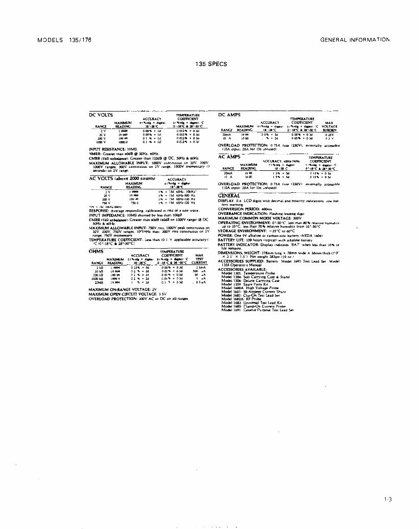
135 SPECS
GENERAL INFORMATION
l-3


MODELS 135/176 ACCESSORIES
Section 2. Accessories
2-1. GENERAL This sect,on describes the various accessor,es and opiio”s avatlable ior use wth Ihe Models 135 and 176. Some of the followlng accesswe are for use only vath the Model 135 and some are for use onlvwlth the Model 176~ These accessoi~es w,ll be clearly potnted out as ,o
which instrument they are used wlth~
2-2. MUTUAL ACCESSORIES The following accessories can be used wrh e,ther rhe Model 135 or the Model 176.
2-3. Model 1 SOOA High Voltage Probe The Mode! 16OOA extends the DMM to 40kV. it has a 1000: 1 d,v,s,on rar,owhich means that 1 volt on the DMM
Corresponds to 1 kV To Operate: Set the DMM to DCV and 200 Volt range, Connect the all~garor CLIP on the Model 1600Ato source Iowa Connecl rhe probe top to so”ice high. Specifications:Voltge Range: 0 to 40.000 volts DC Input Reslsrance: 1000 megohms. Dlvlsion RatlO. 1000 I Ratto Accuracy~
1000 to 1 +2% terminated in IOMR 2000 to : +5% terminated I” I Mn
FIGURE 2-1 1600 HIGH VOLTAGE PROBE
2-4. Model 1651 50 Ampere Shunt The Model 1651 allows current meawrements to be made from 0 to 50 amperes DC and from 10 to 50 am- peres AC, It 1s a 0.001 ohm *l% 4.terminal shunt. A fifty ampere current WI,, correspond to 50 m,ll,volts~
To Operate: Connect separate current leads (not fur- mshed) between the source and the Model 165 1 hex- head bolts. Use leads that are rated UP 10 50 ampere cap.xW Connect thevoltage leads ifurnlshedi between the Model 1651 screw termmals and the DMM INPUT terminals. Set the OMM 10 ACV and 2V range or DCV and 2V range,
2-6. Model 1681 Clip-On Test Lead Set The Model 1681 contains two leads I 2rr 146 inches, long. lhat are terminated w,th banana piug and sarong- acI10” cltp-on probes.
FIGURE 2-3 CLIP-ON TEST LEADS
2-6. Model 1682A RF Probe Model 1682A RF Probe allows voltage measuremenrs from 1 OOkHz to 250MHz
To Operate: Set the DMM to DCV and appropriate range Connect the Model 1682A to the DMM input ,acks Specifications AC to DC Transfer Accuracy: (7.3X? 5°C) tld6 !rom 1OOkHz to 250MHz at 1V. peak iespondlng. calibrated i” ims of a slnewave. compat,ble with 1”5lr”ments wiin 1OMR Input res.,srance
Voltage Range: 0.25V to 15V rms Maw&m Aliowable Input: 50V AC peak. 2OOV (DC+ AC ~eakl Makmufk Common Mode Voltage. 30V rms. 42 peak Input Capacitance: 5pF Typical OperarIng Temperature: 0” to 50°C Cable Length: 1~5 meters Accessories Supplied: ENC Adapter. insuiaring TID, IC Tip. Spring Hook. Carrymg Pouch
FIGURE 2-2 1651 50 AMPERE SHUN1
FIGURE 2-4 1662 RF PROBE

ACCESSORIES ACCESSORIES
2-7. Model 1663 Universal Test Lead Kit 2-7. Model 1663 Universal Test Lead Kit Two test leads. 1.2m (48 inches) long w,th 12 screw-in Two test leads. 1.2m (48 tnches) long vat,, 12 screw-in tips. 2 banana plugs. 2 spade lugs. 2 alligator clips wfh tips. 2 banana plugs. 2 spade lugs. 2 alligator clips wfh boors. 2 needle ups w,th chucks and 4 heavy duty ftp boors. 2 needle ups w,th chucks and 4 heavy duty ftp Plugs plugs.
MODELS 135/176
FIGURE 2-7 1691 TEST LEAD SET
Z-10. MODEL 135 EXCLUSIVE ACCESSORIES
2-l 1. Model 1304 Soft Carrying Case and Stand. The Model 1304 IS a soft carrying case and stand (t,lt baili for Kelthley’s hne of hand held instruments.
The instrument can be secured Inside the case wfth the thumbscrew (suppledI. if dewed, The thumbscrew IS also used 10 secure the stand (tilt bail) fo set the ,nsfru- men! upnghf.
FIGURE 2-5 FIGURE 2-5 1683 TEST LEAD KIT 1683 TEST LEAD KIT
2-S. Model 1686 Clamp-On AC Current Probe 2-S. Model 1686 Clamo-On AC Current Probe The Model 1665 meawres AC current by clampIng onto The Model 1665 mea?.“& AC current by clampfng onto a s,ngle conductor. Interrilptmn ot the current path IS a s,ngle conductor. Interrilptmn ot the current path IS unnecessary, The Model 1665 detects current by sensing unnecessary, The Model 1685 detects current by sensing the magneuc field produced by the current flow. the magneuc field produced by the current flow.
To Operate: Set the DMM to ACV and the appropriate To Operate: Set the DMM to ACV and the appropriate range. The DMM WI, dtsplay O.lV rms per ampere. range. The DMM WI, dtsplay O.lV rms per ampere.
FIGURE 2-S 1685 CLAMP-ON AC CURRENT PROSE
2-S. Model 1691 General Purpose Test Lead Set The Mode, ,691 General Purpose Test Lead Se1 CO”SIS,S of fwo 0,9 I mm (36 Inches) test leads wirh probe ups iermlnated I” banana plugs
2-2
FIGURE 2-8 SOFT CASE AND STAND
FIGURE 2-9 1306 DELUXE CASE
2-12. Model 1306 Deluxe Carrying Case. Model 1306 Deluxe Case is a rugged DMM carwng case that IS large enough to accommodate the 135 plus var- IOUS other DMM art~cies such as a spare battery. fes, leads. ew

MODELS 135/176 ACCESSORIES
2-13. Model 1369 Spare Parts Kit The Model 1359 is a spare parts kit for rhe Model 135 It CO”SISIS of a compIeme”t oi specially seiected spare pans fhar wlil manta!” several 135 DMM’s for one year The parts are INsted I” Table 6-2 of Sectlo” 6. Replace- able Parts,
2.14. MODEL 176 EXCLUSIVE ACCESSORIES
2.16. Model 1010 Rack Mounting Kit The Mode, 1010 Rack Mounting Kit permits the mou”,- ,ng of a single DMM to a standard 5-l 14 in x 19 i” rack
2-16. Model 1017 Rack Mounting Kit. The Model 1017 Rack Mounting Ktt permits rhe mount- ,“g of two DMM’s s,de by sde I” a srandard 5- 1 /4 I” x 19 I” lack.
2-17. Model 1684 Hard Shell Carrying Case The Mode, 1684 hard she,, carrv~ng case IS a hard wny, case which is 4 I” v 13 I” Y 14 I” (100mm x 300mm x 350mml~ Ii has a fltfed foam lnserf wth room for 1he DMM. ~“struct!o” book and small accessories
FIGURE 2-10 HARD CASE
2-18. Model 1766 Battery Eliminator The Model , 766 Batrerv Ei,m~“ator permits the user to operate the 176 or 169 from lhne power. The 1766 pro- vldes the necessary DC voltage to Operate the 176 or 169. The 1766 firs I” piace of the battery pack (Model 1766) so therefore, precludes the use of the battery pack (Model 1768). The Model 1766 is capable of working from a wde range of line voltages such as from 1 OSVAC to 250VAC to 50HZ or 60HZ.
FIGURE 2-l 1 1766 ELIMINATOR
BAmEAY BATTERIES HOLDER
FIGURE 2-12 SAl-rERY PACK
2-20. Model 1769 Spare Parts Kit The Model 1769 1s a spare parts ii, for ,he MOdeI : 76 it co”sIsts of a compiement of SPeclallY seiecreo space parts that WIII ma~ntai” several 176 DMM’s lor cne veai The parts are listeci I” Table 6~3 01 Seci~on 6 Rep!aceaale Parts,

MODELS 135/l 76 PERFORMANCE “ERlFlCATlON
Section 3. Performance Verification
3-1. GENERAL This secf~on gtves a Performance Verilvzat~on procedure for both the Model 135 and the Model 176. Each proce- dure wtil be presented separately I” order to avo,d con- fus,on,
3-2 Performance Verlficatlon may be performed upon recetpt of enher ~nstr~rnenf (1 35 or 1761 10 ensure that no damage or m,sad,ustmen, has occurred dung trans,,. Verlficatlon may also be performed whenever there IS quewcr of elther instrument’s acculacv and foIlowIng cahbraron. if desired.
NOTE
3-3. Environmental Conditions For Both Instruments In order to perform the Performance Verlflcatton the instr~men, to be venfied m”st be between 1 B’C to 2B’C at less than 80% R.H.
3-4. Recommended Test Equipment Recommended test equipment for performance verlfl- cat,on of both instruments IS hsted in Table 3- 1 Alternate test equipment may be used. However. 11 the accuracy IS not at least 3 ttmes better than the instruments speclfl- camns. addlnonal allowance mwt be made m the read- I”@ obtalned.
WARNING
All service information is intended for qualt- fied electronic maintenance personnel only.
WARNING Some procedures require the use of high volt- age. Take care to prevmt contact wth lwe circuits which could cause electrical shock resulting in injury or death.
CAUTION
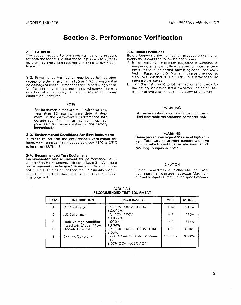
TABLE 3-1 RECOMMENDED TEST EQUIPMEN
ITEM DESCRIPTION SPECIFICATION
A DC Calibrator 1v. 1ov. 1oov. 1ooov i-0.002%
B AC Calibrator 1v. IOV. IOOV +0.022%
C High Voltage Amplifier 1 ooov (Used wth Model 745Ai *0.04%
D Decade Resistor 1K. 10K. IOOK. 1000K. 10M +.02%
E Cuirenf Calibrator 1 mA. I OmA. 1 OOmA. 1 OOOmA. 10A
+.03% DCA. +.05% ACA
3-1

PERFORMANCE VERIFICATION MODELS 1351176
3.6. MODEL 135 PERFORMANCE VERIFICATION
3-7. DC Volts Verification A Select ihe WV funann. B. Connect the DC Calibrator ,ltem A. Table 3-I) to the
135 V-R and COM fermnals. Refer to Figure 3- 1 C~ Follow Table 3-2 and apply the required DC Voltage
fo, each range, “er~fy rhat each reading IS WI,,,,” spec- iltcatlons iwed tn Table 3-2.
D, Repeat all checks with nega1,v.s voltage
TABLE 3-2 DC VOLTAGE PERFORMANCE CHECK
Range Applied Voltage
Allowable Reading at 18’C to 28°C
FIGURE 3-l 135 DC VOLTS VERIFICATION
3-6. AC Volts Verification A~ Select the ACV functmn. B. Connecr the AC calibrator (Item 8. Table 3-l) to the
135 V-Rand COM termlnais. Refer fo Figure 3-2, C, Follow Table 3-3 and ~DDIY the reaulred AC Voltaae
for each range. Venfy th’ai <he reading IS wlfhtn speci- ftca11ons Wed I” Table 3-3.
TABLE 3-3 AC VOLTAGE PERFORMANCE CHECK
Range Applied Voltage Allowable Reading at 18°C to 28’C
l,OOOOVat 10KHz ~9885 to LO1 15 I O.OOOVat 500Hz 9,885to 10,115
2oov 100OOVat120Hz 98.85to 101,15 I
FIGURE 3-2 135 AC VOLTS VERIFICATION
746A P
FIGURE 3-3 135 HI VOLTAGE ACV VERIFICATION
3-9. Resistance Verification A. Select the OHMS funcrlon By Conneci rhe Decade Resistor (Item 0. Table 3- 1) tothe
135 V-s2 and COM terrmnals. Refer 10 Flgure 3-4, C. Follow Table 3-4 and apply the requfred ressstance
for each range. Vertfythat each read,ng isw,th,n soec- lficatrons Ifsted in Table 3-4
FIGURE 3-4 135 RESISTANCE VERIFICATION

MODELS 135/l 76 PERFORMANCE VERIFICATION
TABLE 3-4 RESISTANCE PERFORMANCE CHECK
i
Range
2KR ZOKR
200Kfl 2000KR
20MR
Allowable Reading at 1wc to 28Y
9970 to 1,003o 9.978 to 10.022 99.78 to 100.22 997.8 to 1002.2 3.898 to 10.102
3-10. DC Amps Verification A, Select the DC Amps function. B. Connect the DC Calibrator ,l,em A. Table 3- 11 10 the
tnput of the Current Calibrator (Item E. Table 3-l I Connect the OU,,,U, of ,he Current Calibrator to the 135’s mA and COM terminals. Refer 10 Figure 3-5.
C. Select the 20mA range and apply a 10,OOmA curren, to the 135. Ver,fv that the reading IS with,” 9,93 to 10.07.
D. Select the 1 OA range and connect the outp”, of the Current Calibrator 10 the 135’s 10A Hi and 10A LO terminals Refer to Figure 3-6
E. Apply lO.OOA to the 135 and ver,fy tha, rhe reading IS w,,h,” 3.88 to 10.12,
3-11. AC Amps Verification A~ Select the AC Amps functlon and the 20mA range. 8. Connect the AC Calibrator (Item B. Table 3-l) to the
mput of the Current Calibraror (Item E. Table 3-11 Connect the output of the Current Callbrafor to the 135’s mA and COM term~nais. Refer 10 Figure 3-7
C~ Apply a 10,OO mA currenr a, 500H2 and verliy lhal the readfng IS w,th,n 9~80 to 10.20~
D. Select the 10A range and connect fhe outp”, of the Curren, Calibrator fo the 135’s 10A HI and 1 OA LO terminals. Refer fo Figure 3-8.
E. Apply a 1 O.OOA current at 500Hz and ver,fv that fhe readang IS wfhin 9.80 10 10.20.
343A
343A
FIGURE 3-6 135 1OA DC AMPS VERIFICATION
FIGURE 3-7 135 AC AMPS VERfFlCATlON
FIGURE 3-5 135 DC AMPS VERIFICATION
FIGURE 3-8 135 ,OA AC AMPS VERIFICATION

PERFORMANCE VERIFICATION MODELS 135/l 76
3-12. MODEL 176 PERFORMANCE VERlFlCATlON
3-l 3. DC Volts Verification A. Select the OC Volts functuon. 6. Connect the DC Calibrator IItem A. Table 3-l) to the
176’s HI and LO ~npu, ierminals. Refer to Fig’ure 3.9. C. Follow Table 3-5 and apply the required DC Voltage
for each range, Verify tha, each readtng IS wtfhin spec- ifications Ifsted I” Table 3-5.
D. Repeat all checks wtth negatwe voltage,
TABLE 3-5 DC VOLTAGE PERFORMANCE VERIFICATION
Range Applied Voltage
Allowable Reading at 18°C to 28°C
I 4’ 1
I J
FIGURE 3-9 I76 DC VOLTS VERIFICATION
3- 14. AC Voltage Verification A. Select rhe AC Volts funcuon. By Connect the AC Calibrator and HVAmpllfier iltems B
and C. Table 3-l) to the 176’s HI and LO terminals. Refer to Figures 3-10 and 3-1 1.
C. Follow Table 3-6 and apply the required AC Voltage for each range. Verlfythafeach reading iswithIn spec- lflcatlons listed ,n Table 3-6.
TABLE 3-6 AC VOLTAGE PERFORMANCE CHECK
Range Applied Voltage Allowable Reading at 18°C to 28°C
;:: 1 1 ~OOOOVa, OOOOV at 1 OKHz 1 KHz .9885 ,9885 to to 1.01 1.01 15 15
2% 1 1 ,OOOOVat O~OOOV at 20KHz 1 KHZ 9,885 9485 to to X0515 10,115 2ov lO.OOOVat 1OKHz 9.885 to 10.1 15 2ov 10,OOOVar 20KHz 9.485 to 10.515
2oov 100 OOV a, 1 KHz 98.85 10 101,15 1 ooov 1OOOOVal IKHz 988.5 to 101 1 5
FIGURE 3-10 176 AC VOLTS VERIFICATION
FIGURE 3-l 1 178 HIGH VOLTAGE ACV VERIFICATION
3-15. Resistance Verification A, Select the OHMS funcnon. 8 Connect the Decade Re%$,or (hem 0. Table 3-I) to the
176 HI and LO ~npu, terminals. Refer to Figure 3.12. C, Follow Table 3-7 and apply the reqwred resistance for
each ranae. Verlfv that each readina is within soeclfl- cations ll;ted in fable 3.7~
TABLE 3-7 RESISTANCE VERIFICATION
Range Applied Resistance
Allowable Reading at 18’C to 28’C
I 1
FIGURE 3-l 2 176 RESISTANCE VERIFICATION
3-4

MODELS 135/176 PERFORMANCE VERIFICATION
3-16. DC Amps Verification A. Select the DC Amps tunctton. 8. Connect the DC Calsbrator (Item A. Table 3-l I to the
,nputottheCurrentCai,bra,~r ,ltemE.Table 3-11, Con- necf the output 01 the Current Calibraror to the 176 HI and LO l”p”r terminals. Refer to Figure 3- 13.
C, Follow Table 3-8 and applv the required c”rrenf for each ranges Verliy ihat each reading IS wrhln spew flcatlons ilsted I” Table 3-8,.
TABLE 3-6 DC AMPS VERIFICATION
Range Applied CtlrrWlt
Allowable Reading at 16°C to 26°C
3-17. AC Amps Verification A. B.
C,
Select the !iC Amps funwon Connect the AC Callbraror jlrem 6. Table 3-1, to the ~“puiotIheCurrentCaiibrator,ltemE,Tab,e3-ti Con- nect the Outpu! of the Current Callbraior IO the 1 76 Hi and LO termnals Refer to F,gure 3-14 Foliow Table 3-9 and apply the required curient for each range. Vertiy that each reading 1s warhtn spew,- cations ksted in Table 3-9
TABLE 3-9 AC AMPS VERIFICATION
I I Range Applied Current
I Allowable Reading
a* 19°C to 26°C
2mA 1~OOOmA ~993 IO 1~007 2mA 1 .OOOmA at 1 KHz 980 to 1320 20mA 1 O~OOmA 9.93 10 10.07 20mA I O.OOmA ar 1 KHz 9~80 10 IO 20
200mA 100 OmA 99.3 to loo,7 20OmA 100,OmA at 1 KHz 9aoto 1023 2000mA 1000 rnA 993 to 1007 2000mA lOOO,mA at IKHz 980 10 1020
343A
FIGURE 3-13 176 DC AMPS VERIFICATION
FIGURE 3.14 176 AC AMPS VERIFICATION
3-5


MODELS 135/l 76
Section 4. Theory of Operation
4-l. GENERAL and graphs. Detacled st~emaiics of ,he Moaei 135 a”~ Model 176 are orovlded ,n Sewon 6
THEORY OF OPERATION
Th,s sect,on contatns the c,rc”~, descrtpflons for The Model 135 and Model 1 76. The iollowng dlscusslons of c,rcu,t theory veil be separated <“to 2 maw sect\ons~ The 2 map, SeCtIOnS are:
I ) Model 135 Circuu Theory 21 Model 176 Czrcutt Theory
The ~nfprmat,on contaned I” each of these 5ectto”s IS arranged I” the following manner.
1, Overall Functional Description 7.1 Stgnal Condittonrig 3) A/D Converter 4) Display 51 Power SUPPlY
To facilnate understandtng. each descrtptton IS accom- panted wth slmpilfied schematIcs. blockdlagrams. tables
V-Q ATTENUATOR
RESISTANCE
4-2. MODEL 136 OVERALL FUNCTIONAL DESCRIPTION
The Mode, 135 1s a 4-1 i2 aqr. t20.000 co”“, hard held DMM It has 4 DC voltage ranges. 4 AC voltage ranoes. 5 res,srance ra”aes. 2 DC C”rre”l ranoes ant 2
The 135 was destgned for h#gh periormance ar zov? cosi To meet these design goals the 135 takes advantage r,’ standard <off the shelf” components, The A/D c~)“vertel was designed from scratch using dlscrete componenls for lower power ‘onsumpt\on and ,mproved aeriorman:e over prssen,ly available LSI A/D converters
Ftgure 4- 1 shops the overa,, bioce diagram 1-r xw mc^ei 135
+e.4v -5V ANALOG IAC CONVERTER ONLY) +5V ANALOG
+5V DIGITAL
ANALOG
FIGURE 4.1 135 BLOCK DIAGRAM

THEORY OF OPERATION MODELS 135/l 76
4-3. Signal Conditioning The Signal Condltlonlng for the Model 135 includes DC arten~atmn iexcept on the 2 Volt range,. AC attenuation. AC/DC conveis~an. Ohms conversion and current ShUrxS. A. DCV Signal Condittonlng consists of one lOMnpas-
swe dwder~ The taps tram this divider are inputted dlrecrly to rhe A/D converter through the rotary range watch S102. Table 4-1 state~~he associated attenua- tton with each range, Potentiometer Rl 13 trims the ga,n for the 20 Volt range. The overload protection IS provided by the llmmng resistor Rl 15. C
TABLE 4-1 ACV AND DCyA7TENUATlON
Rl 1 1 establishes AC zero while R 109 determ,nes the full scale gain (19000 counts), R105 and C 108 pro- vlde the low pas5 f,lter ro average the half wave recw fled outputs Overload protection IS prowded by d,odes CR104 ahd CR105 and currentllmttlngreslstorR1 10. Figure 4-2 shows a simplified SchematIc of the AC cOn”erter.
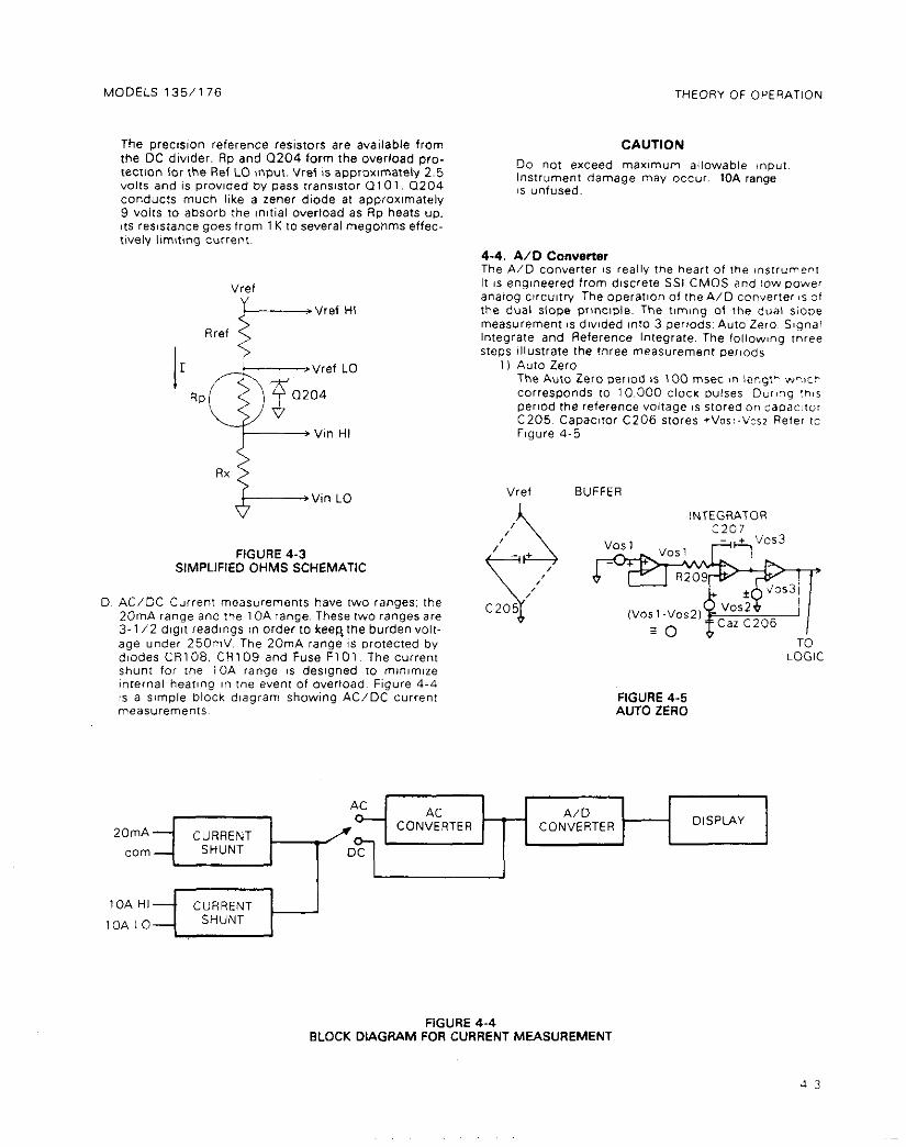
Resistance Signal Condltloning 1s accomplished iax- metrically. That IS. a precision reference resistor and Rx are put in ser,es wth a 2,5 volt reference, There- fore. the current developed i” the two ~BSIS~IIS 15 the same. Taking the ratlo of rhe voltage drop across Rx 10 the drop across R<e,e,en<e coriectly caiculates ohms. The value of the voltage reference IS irrelevant. as ,t only serves to apply a source of currentto the ies,stors (Rx and Rrc~ewncel. The preceding theory IS illustrated mathematically in the following equations. Refer to Figure 4-3,
I = Vref Rref + Rp + Rx
‘75OV range for ACV
B. ACV SIgnal Condmonmg consists of a 1 OMR pasSwe dwlder. AC buffer amplifier and AC co”verWr. The scalmg IS accompi~shed by the same 10MSIwsswe dlwder that IS used for DCV scaling, After the divider rhe :,gna, IS AC coupled ,nto U105 the AC Buffer Ampl~flei. The slgnai is then applied 10 the averaging piec~~~on rectlfler U 104, It IS driven at low lmpedan.ce by the AC coupled buffer U104 performs the AC con- version, It then passes through a two stage low pass filter which converts it to DC. This OC level IS applied fo the A/D converter. Input resistance for the AC con- verter is 1 OfvUlshunrea by less than 100 pf.
Vdisplay = ;;;f;,:;;;f$ X 10,000
Vdisplay = I [Rx1 -0 lL~ref+flp+R~]-i[~p+~xJ x’o.ooo
IRX Vdisp’av = , [Rref + Rp C Rx. Rp. Rx] x 10.000
Vdisplay = & X 10.000 = & X 10.000
lOMR DIVIDER v2v
AC COUPLING
7
2ov f---l* BUFFER PRECISION TWO STAGE
UlO!i - RECTIFIER - LOW PASS - u104 FILTER
R105 Cl08
! 2oov
90KR
750v
1 OKR
FIGURE 4-2 SIMPLIFIED AC CONVERTER BLOCK DIAGRAM
4-2
MODELS 135/176 THEORY OF OPERATION
The prectsion reference resistors are wallable from the DC divider. Ap and Cl204 form the overload pro- te~llon for the Ref LO ,“put “ref is approxnnately 2.5 volts and is provided by pass rrans~stor QlOl, 0204 conducts much like a zener diode at approxlmafely 9 volrs to absorb the imtial overload as Rp heats up. 16 res,stance goes from 1 K to several megohms effec- ttvely limttrig cuireni.
h--- Lo FIGURE 4-3
SIMPLIFIED OHMS SCHEMATIC
D AC/DC Current measuremenrs have two ranges: the 20mA range and the 1 OA range. These two ranges are 3-l/2 d,g,t readings in order to keep, the burden volt- age under 250mV, The 20mA range IS protected by d,odes CR1 08. CR1 09 and Fuse Fl 01. The cuirent shunt for the 10A range IS destgned to m,n,mize ~ntetnal heatlng I” the event of overloads Figure 4-4 is a simple block diagram showing AC/DC current measurements~
CAUTION
Do not exceed maxtmu” allowable input Instrument damage may occur, 10A range IS unfused.
4-4. A/D Converter The A/D converter IS really the heart of lhe znstrumer, If 6 engmeered from dlscrere SSI CMOS and low powe, analog circuitry The operation of rhea/D converter 1s of the dual slope pr,nc,ple. The tuning of rhe dual siope measurement IS dwded into 3 pertods: Auto Zero, Sgnai Integrate and Reference Integrate. The fo,low,ng fhree SIeps lll”Strate the three measurement pertods
1, Auto Zero The Auto Zero per,od is 100 rnsec in !engt* v11tzr corresponds 10 10.000 clock pulses Dw?g :n,s period the reference voltage IS stored on caoacilc: C205~ Capacllor C206 stores +vos:-v~s2 Refer tc Figure 4-5
Vref BUFFER
INTEGRATOR
FIGURE 4-5 AUTO ZERO
DISPLAY
FIGURE 4-4 BLOCK DIAGRAM FOR CURRENT MEASUREMENT
THEORY OF OPERATION MODELS 135/l 76
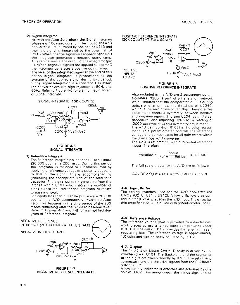
21 Signal Integrate As wtth the Auto Zero phase the Signal Integrate phaseisof lOOmsecdurat~on.The~nputafrheA/O converter is first buffered by one half of U2 13 and lhen the signal 1s integrated by the other half of U213. When pOSitlveSignaiSareapplledtotheA./D the ~nregrator generates a negawe go’ng ramp. Thus can be seen al the output of the lntegraror ip~n 1). When negative signals are applied IO the A/D the mregrator generates a powwe going ramp. The level of the mtegrated signal at the end of this permd islgnal integrate) is proportional to the average of the appiled s!gnal during th!s pewd. Since Signal Integration is a constant 100 “sec. the converter exhibits high rejectron at 50Hz and 60Hz. Refer to Ftgure 4-6 for a slmpilfled dtagram of Signal Integrate.
SIGNAL INTEGRATE (IOK COUNTS1
FIGURE 4-6 SIGNAL INTEGRATE
3’1 Reference Integrate The Reference Integrate pernd for a full scale8nput 120.000 counts) is 200 “sec. During this period the fntegrator is returned 10 a baselrne level by applying a reference voltage of a polaray opposne to that of the slgnal. This IS accomplished by grounding the appropriate side of the reference capacator~ The dtgltal output IS generated from the latches wlthtn UlOl which store the number of clock pulses required for the lntegraror to return to baselme levels. For inputs le?,s than full scale ifull scale = 20.000 countsI. the A/D automatically reverts to Auto Zero. This happens I” the rime period of the 200 msecs remafmng after the return to baselme level. Refer to Figures 4-7 and 4-8 for a slmplifled dia- gram of Reference integrate.
NEGATIVE REFERENCE INTEGRATE (20K COUNTS AT FULL SCALE)
NEGATIVE INPUTS TO A/D
FIGURE 4-7 NEGATIVE REFERENCE INTEGRATE
POSITIVE REFERENCE INTEGRATE (ZOKCOUNTSAT FULL SCALE)
INPUTS TO A/D
FIGURE 4-8 POSITIVE REFERENCE INTEGRATE
Also Included rn the A/D are 2 adjustment poten- t~ometets. R205 is part of a translation network which Insures rhat the comparator ourplit during autozero IS at or near the threshold of U204C. which is ihe zero crosstng flip flop. Therefore thus adlustment controls symmetry between posmve and negative jnputs Shorting C204 (as I” the cal procedure) and adjusttng A205 for a reading of ~0000 accomplishes this symmetry adjustment. The A/D gal” control (R102) IS rhe other adlust- men,. This potentiometer controls the %ference voltage and compensates for all gain errors wlthfn the dual slope A/D converter, The A/D is rat~omerr~c. with dlfferenrlai reference fnputs~ Therefore
Vd6play = (Ref ;‘““;if Lo) x 10.000
The full scale inputs for the A/D are as follows:
ACV.DCV.fi.DCA.ACA = +2V (full scale input)
4-5. Input &dfer The analog watches used for the A/D converter are CMOS (U210. U2 1 1. U2 121. A low drift. low bias cur- rent buffer iU2 141 precedes the A/D input. The offsel for thfs amplifier iU2 141 1s nulled w(Ih potentiometer R207.
4-6. Reference Voltage The reference voltage (Vwl IS provided by a dlwder net- work placed acnxs a temperature compensated zener (CR1 101. One half of U 102 prowdes the zener wrh a self regulamg bias, The reference voltage IS approx~marely 1.0 volts and can be fmely adjusted by R102.
4-7. Display The 4-l/2 digIt Llquld Crystal Dlspiav IS driven by LSI counter/driver U 10 1~ The Backplane and the segments of the dtglts are driven dlrecrly by UlOl The zebra strip connector transfers rhe dwe slgnais from the P-C board Onto the LCD~ A low battery mdlcator is detected and actuated by one half of U102. Thts an”““c~atcx. the minus srgn. and a,,
4-4

MODELS 135/176 THEORY OF OPERATION
declmal pants are dwen by the exclusive OR gate arrays U201 and U202. The dtgmzed measuremen, data IS presented by out- Put ifnes IO rhe LCD, These lines are dwen by a square wave having the same ampiltude and ‘reauency as rhe Backplane l,“e. When rhe ii”e5 IO the d,splay segmenrs are driven 180” our of phase with the Backplane the seg- ments are ON. Conversely. when tn phase the segments are OFF The dectmai points and rhe LO battery #ndlcaror are Turned OFF and ON s,m,larly.
4-8. Power Supply The prec,s~on reference current source “102A also dou- bles as the +5 volt supply. P,n 1 of U 102 IS the V+ supply The 5 volt supply IS generated by a power ~““erter c~rcui, (U1031. This device charaes capacitor C 102 and then rwerses it. Thts effect,“& gene;ates -5 “pits. A “oi&,ge doubler c$rc”tt consisting of C.103. C104. CR101 and CR102 generates +8.4 KITS. Th,s voltage IS only used on U104 which is the precision recttfler amplifier iUlO4) of the AC co”“erter.
4-9. MODEL 176 OVERALL FUNCTIONAL DESCRIPTION
The Model I 76 IS a 4. I /2 diglf. f20.000 count portable bench DMM It has 4 DC “&age ranges. 4 AC “oirage ranges. 5 ie~iSta”ce ranges. 4 DC current ranges and 4 4C current ranges. Along w,th theselunct,onsand ranges tt has 100i.1VDC and AC “offs senstttvlty with 100mQ res~siance se”~m”~ty The DC and AC current senstt>“,,” IS 1uA. The 176 was destgned for h,gh performance at tow cosr To meet these design goals the 176 lakes advantage 01 standard “off rhe shelf” components. passive s~g”aI con- dltionlng and multlfuncrion components and CI~CUIIS, The A/D converter was designed from scratch us,ng dlscrere SSI CMOS c~mppnent~forlowpowerconsump- r!on and improved performance-aver presently available LSI A/D converters.
OHMS REFERENCE
/
VOLTAGE
RI .d
TABLE 4-2 ACV AND DCV ATTENUATION
Rang.? Attenua~,on Factor
2V ‘1 2ov i’ 0
2oov +i so I ooov ?lOOO
A/D CONVERTER
OlSPL4Y
ATTENUATOR ANNUNCIATOR DRIVERS
I I +8,4V -5V
IAC CONVERTER ONLYY) +5V DIGITAL +?JV ANALOG
FIGURE 4-9 DIGITAL
176 BLOCK DIAGRAM
J-5

THEORY OF OPERATION
ZVRANGE R103
MODELS 135/176
R106 8.9775MQ 2OV RANGE
-
R108
gaoK~ _“_. .,, ..--
R108 ilO 90KR 1OOOVRANGE
R108 9KR
A108 1KR
1-2 VOLTS TO +2 VOLTS)
FIGURE 4-10 DCV SIGNAL CONDITIONING
4-12. AC Volts The AC Volts Signal Cond,!,on,ng cons,s~s of a passive d,v,derfR109-Rl 11.Ri 14andC103~C106)andfheAC converter During AC “okage measurements the meas- ured sqnal IS aopl,ed 10 ihe dlwder and IS atten”aIed by 1,10.l00or1000forthe2V.20V.200orlOOOVrange respectively, The capacitors (C 103 C 1061 are used for ~orni)e”salion for stray capacitance and for frequency characrer,st~cs of rhe resisrors, There IS no capaaror used on rhe 2V range for frequency compensation There are onlytwocapacitors ,nrhecircu,tforanyotherrange~Th,s reduces ,nteract,on between ranges and allows easy ISO- lhon of taulrv capacitors~ The outputfrom the AC dlvtder IS appl,ed to rhe AC converter where 8, IS recflfled and scaled before being appI,ed to the A/D converter, Refer to Figure 4-l 1
.-’ +, _ , ~107 R116 _. - _
>E d-&,%-TO AC CONVERTER
J. --_ lOOKa PROTECTION
OPEN. C103. C104. Cl05 DEPENDING ON RANGE
R109 ilooo lKS2
FIGURE 4-11 AC VOLTS DIVIDER
The AC converter IS a preclson half wave reci~f~er with high mpedance fnput and sufflclenr gal” 10 produce a DC output equal to the ims value of a sine wave input Following the sIgnal path. C 107 1s used as a DC blocking capac~ror so thar DC oftsets ,n rhe measured signal do no1 affect fhe readmg. UlO8 IS a unify gain buiier used lo eliminate loading 01 the AC dlwder and prwde Iow im. pedance dwe for rhe acfual AC converter ” 109 Capa,- tom C 109 and Cl 10 eliminate any problem due to the offset voltage of U 108~ Rl 19 R 12 1 ad,us, the gal” of the AC converter required to convert from fhe rect$hed waveform average 10 rms equ~“aIeni, Resistors RI ! 7 and 4 1 18 adlusr 0~1 any error at zero due ro oifsers I” ” 109 U 109 uses feed forward compensation provided by C 1 14 and will become unsiable when any capac~riue load isuch as a scope probe) IS attached near rhe ou1pu1 cjrcuitry 01 the CIP amp lU109)~ Refer 10 Figure 4.12
R120 I-DCD’J’
AC Cal CR107
Al 19
R118 50KR ZERO AD.!
FIGURE 4-12 AC CONVERTER
4-6

MODELS 135/l 76 THEORY OF OPERATION
tars RI 07a;d R 108 are a150 the DC” dtvider, Us,ng the 1KR. 10KQ. 100KR. IOOOKn and 10MQ tapson the dwder for ihe 2K.Q. 20Kn. ZOOKR. 2000Kfi and 20MR ran4e5,ihedls~lavedreadlnaistheac1ualres,si-
lOKI2 PROTECTION
PROTECTION “,.‘,:“, T
INPUT> h
4iOKn PROTECTION
+--REF LO
II PROTECTION
h INPVT HI
UNKNOWN RX RESISTOR
6
INPUT LO
Input HI Input LO Ret HI Ref Lo
FIGURE 4-14 OHMS SIGNAL CONDITIONING SIMPLIFIED
TO A/D INPUT 6”FFtR OR AC CONVERTEP
lNP”T
R106 0 1R
INPUT--------/i
FIGURE 4-13 OHMS SIGNAL CONDITIONING
FIGURE 4-l 5 AMPS SlGNAL CONDITIONING

THEORY OF OPERATION MODELS 135/176
4-15. Input Buffer
FOLDOVER PROTEC- TION RESISTOR ON BOTTOM SIDE OF PCB
UllO ON REV C PCE’S.
C1’18
FIGURE 4-16 O.lpF
INPUT BUFFER
4-16. A/O Convener The 176 A/D converter is essent~allv the heart of the instrument. It has been engineered wrh discrete SSI CMOS and Ibw power analog c~rcu,fry. This A/D con-
The Auto Zero period IS 100 msec I” length whtch corresponds to 10.000 clock pukes. Dur,ng th\s perlod the releience voltage IS stored on capacitor c 1 1 7. capac,ror c 120 stores +Vasl “os2. Refer to Figure 4-1 7.
21 stgm Integrate As wth the Auto Zero phase the SIgnal integrare phase 1s of 100 msec duralton. The input of the A/D converter IS f,rst buffered by Ul 10 and then II IS integrate0 by Ul 11, When posmve s,g”als are applied to the A/D the ,nfegrator generares a nega- we gang ramp. This can be seen ar the output 01 the !ntegrator (pin 11~ When negative signals are applted to the A/D rhe integrator generates a pas,- we go,ng ramp. The ieve, of rhe integrated signal at me end of fhls period tslgnal lntegratei IS proportional to the aver- age Of the applied s,g”al dur>“g ,h,s pert& S,“ce SIgnal Integrate IS a constant 100 msec. the A/D co”“e~ter exh,b,ts h,gh re,ect,o” at 50Hz and 60Hz, Refer 10 Ftgure 4-l 7.
3) Reierence lnteglate The Reference Integrate perlod for a full scale ,nput (20.000 co”nls, IS 200 msec, During rh,s period the
INTEGRATOR Cl19
COMPARATOR ITAANSISTORS 010,. 102. 103,
RE! LO
FIGURE 4.17 A/D CONVERTER
4-8

MODELS 135/l 76 THEORY OF OPERATION
,ntegraror IS returned to a basei,ne level by appiylng a reference voltage 01 a p&my oppos~re to that of the SIgnal. This IS acompllshed by grounding the appropriate side of the reference capacjtor The d,g,,al output 1s generared from rhe latches wlthln “107 which store rhe number of clock pulses requmd for the integrator to r.?t”rn to basellne levels For ,np”ts Iess than tuil scale ifull scale = 20.000 coun,sl. rheA/D automat~caliy reverts ,oAufo Zero. This happens in fhe fime perNod of the 200 msec rema,n,“g after rhe return to baSelIne level AIs, Included I,. the A/D are 2 ad,ustmeni pore”- tiometers ‘8125 IS part ot a translation network which insures that the comparator output dung Auto Zero is at or near the threshold of VI 14C. wh,ch IS the zero crossjng fltp flop, Therefore thts ad,usrment conrrois symmetry between posweand negmve ~ny)uts~ Shorting C 1 18 jas I” the Cal Proce- dure, and adlusting Rl 25 for a read,ng of 0000 accomplishes this symmetry adjustment, The A/D gan conrio (RI301 IS the other adjust- ment. Th,s potentiometer controls the reference voltage and compensares for all gal” errors wtlhln fhe d”ai slope A/D co”“er,er~ The A,D conver,er is rat~ometrlc wfh d~fferenrial reference inputs, Therefore
Vdtsplay = (Ref ,yil”u,‘,, Lo) x 10.000
The full scale ,nputs for the A/D are as follows: 1. ACV = +2V (full scale mput) 2. DCV = ezv IfUll Scale inDuti 3. n = t2v (full Scale l&Ii 4, ACA = +~2V lfuli scalB InPut) 5. DCA = +.2V (full Scale InPUtI
4-l 7. Protection Circuitry A, DC volts
B
C,
In reierence to Ftgure 4- 10. RI 03 protects the ~“stru- menr from damage by llmitlng the current IO the tnput buffer to about 2mA max~m”m, Extended a~pl~catlOn
of greater than 300 volts on the 2VDC range may damaae Rl 16. AC V&s in reference to Figure 4-l 1, Rl 16 protects the ~nstru- ment from damage by l,m,,,ng rhe curren, to ihe AC converter to approximately 1 OmA maximum. Extended appl,cat,on of greater than 300 volts on the 2V AC range may damage R 103~ Ohms In reference to Figure 4-13. there are three CO”PO- nents that protect Ihe ~nstrumenf in the eve”, voltage 1s appited lo rhe mput whtle on the Ohms lunct~on TheseCompo”entsareR103. RTIOI andQ104, R103 works exacflyitke ildoesforDCvo,tagemeas”reme”,s by limnng current $mo the tnpui buffer amplIfter Q104 1s used as a tow leakage zener with a break- down voltage of app,oxtmately 10 “olts~ RTl 01 1s a positive temperature coeff~ctenf thermistor, RTI 0 1 I,m,ts the curie”, gofng 10 Q104 by increasing its res,stance greatly when heated Thus happens when volrage above 10 volts IS applvzd to the tnput When vdfages of much greater value than 300 volts are
0, Amps LC or DC In reference IO Flgure 4- 15 CR101 pro,ects tne .ow

THEORY OF OPERATION MODELS 135/l 76
power converter which generales -5 volts by chargmg Cl27 with the +5V supply, then switchtng the pos111vB lead of C 127 to ground and charyng C 130 to -5 vOltS~ CR108. CR109. Cl24 and Cl26 form a simple voltage doubler drwen b” Cl 27 The result of the doubler equals +8~4 volts wh,ch is used exclusively by U109 I” the AC COnYerter. The +5 volt supply IS spltr ,nto two separate lhnes, One for the analog c,rcu,try and one lor the diglial ctrcutrry The -5 volt suppiy IS used for rhe comparator. the analog swtches and mosr of the OP amps.
The facr that CR1 I 1 IS stable wfh r,me and temperarure enables it to also be used to deilve the prec,se 1 0000 volt and 0.1000 volt reference signals rhat are used for Volts and Amps. respectively, Durmg voltage measure- ments the CR 1 1 I voltage IS attenuated to 1~0000 volts by Rl 13. Rl 15 and R130~ The 1 ~OOOOV s,gnai IS fed to the A/D reierence ,nput~ During the Amps funcnon fll 15 IS replaced by a secr~on 01 RlOB. Th,s atfenuares the 1,OOOOV to 0,lOOOV wh,ch 1s a&led ,o thk A/D reference (“put,

MODELS 135/l 76 MAINTENANCE
Section 5. Maintenance (Troubleshooting, Calibration)
5-l. GENERAL
Model 135 Caltbrat~on
Model 135 TroubIeshoor<“g
Model 135 Batrery Replacement. Fuse Replacement
Model 176 Cai,brar,on
Model 176 Troubleshooting
Model 176 Battery Replacement. Fuse Repiacemenr
Model 1766 Troubleshooting
5-2. MODEL 135 CALIBRATION The Model 135 recommended cal,bratlon equ,pmen, IS !~sted I” Table 5-l Alternare equipment may be usea However. the atc~rac” of rhe alternate equipment must be ar ieast 3 limes bertei ihan the Model 135’s spec,f,- cat,ons or equal to Table 5- 1 spec,f,catlons~
5-3. Environmental Conditions Callbratlon shoula be peiformed under laboratorycondl- W,“S having a” amble”, temperature of 23°C _+I ‘C and a reiat,ve humld,ty 01 iess than 70%, If the instrument has been sublected to temperaiures outside of this range. or to h,gher hurmd,,“, aI,ow one hour mln~mum for Ihe tnsrrument to stabtlize at the speclf,ed e”v,ronme”tal cond,,,ons before beglnnlng the callbratlon procedure.
5-4. Calibration Procedure
NOTE
Cahbratlon should be performed bYqualifIed personnel “sing acC”rate and reliable eq”,p- ment.
CAUTION
Do nor exceed the max,mum allowable input voltage. Instrument damage maY occur. Max- mum allowable inpuTs are stated I” the spec- ficatlon.
FIGURE 5-1 SOLDER SIDE OF A/D BOARD
) ITEM 1 DESCRIPTION I SPECIFICATION 1 MFR, \ MODEL ) ITEM DESCRIPTION SPECIFICATION MFR, MODEL
A A DC CaI,brator DC CaI,brator :ov 1oov. 1ooov :ov 1oov. 1ooov Fl”klZ Fl”klZ 343A 343A + 002% + 002%
8 8 AC Calibrator AC Calibrator I”. iv. 1ov. IOOV I”. iv. 1ov. IOOV H-P H-P 745A 745A ?022% ?022%
TABLE 5-1 RECOMMENDED CALIBRATION EQUIPMENT

MAINTENANCE MODELS 1351176
Remove the short from C204 Select the 2V range and short the !nput termtnals (VR to COMI, Adjust R207 for ~0000. Remove the short from the input terminals Wlto COM)~ Apply + 1.9000VDC to VRand COM and adjust R102 for +1.9000. Select the 20V range and apply + 19.000VDC to V-n and COM and adjust R1 13 for + 19.000. Select the ACV funcflon and the 750V range. Short the (“put term,nals (V-R to COM) and adfust Rl 11 for 000.0, Select the 2V range. Apply 1.9000VAC at 500 Hz to V-fl and COM and adfust RlOS for 1.9000.
R207 R205 R102 I I
FIGURE 5-2 SIDE VIEWS OF CALIERATION ADJUSTMENTS
5-6. TROUBLESHOOTING The troubleshooting instructions contained I” this section are Intended for quailfled personnel having a basic under- standIng ot analog and dlglt.8 c,rcu,trv used I” a prec,s,on test ,nstrument. The ~ns,r”~t,o”s have been wntten to asssr in ~solat,ng the defective urcuit or subclrcult. IsO- lat,ng the defective component has been left to the tech- DlCla”
NOTE For instruments that are still under warrantv (less than 12 months since date of shipment). If the instrument’s performance IS outside of specafications at any point, contact your Ketthlev representative or the lactorv before attempt,“g troubfeshootlng or repeli other than battery or fuse repiacement.
5-6. Special Handling of Static Sensitive Devices CMOS dewces are deslgned TO functlon ar’very high Impedance levels for low power consumpt~on~ For th,s reason. a normal static charge bu,ld up on vour person or clothing can be suff,cient 10 destrov these dev,ces. The foliowlng steps hst the static sens~twe dev,ces ,n your
Model 135 and provtde instruction on how to avold damaging them when they must be removed or replaced. A. Static sens~we dewces:
Reference Des,gnar,on Keithlev Part Number UlOl IC-286 u102 IC-288 u103 IC-287
u201. u202 IC-226 U203. U209 IC-103
u204 IC-284
0. The above Integrated clrcults should be handled and transported only in protection contamers. Typically they will be received I” anti-static tubes or elecrr~callv conductive foam. Keep the devices in thefr origlnaf containers until ready for use.
C. Remove the devices from their protectfve containers only at a properly grounded work bench or table. and of~lv after grounding yourself by using a wrest strap.
D. Handle the devices only by the body. Do not touch the Pll7S.
E. Any pnnted c,rcu,l board (“to which a de”,ee IS to be inserted must also be grounded to the bench or table.
F~ Use only ant,-stat,c type solder suckers. G. Use only grounded t!p soldering irons. H. After soldering the dewce ,“to the board. or properly
lnsertlng it 1nt0 the matmg receptacle, the devlce is adequately protected and normal handlmg can be resumed,
5-7. Troubleshooting Procedure This section contatns tables ilsttng step-by-step checks of the major DMM circuits described in Section 4. Theory of Operations The following steps outl$ne rhe use of these tables and provide ~nstrucrion for orepanno the DMM for troubleshoot,ng. Read all of thede steps & trow bleshootlng the ,nstrument~ To troubleshoor the wwrumenf 11 $5 necessary TO dwas- sembie the 135 case. To do th,s foilow the steps outlined I” paragraphs 5-4-l. 5-4-2. 5-4-3. A. Power Suoplv
Start off troubleshooting with the power supply in Table 5-1 there are several steps and checks thaw,,, verify If the power supply IS ProVldirIQ the appropriate voltage to the c,rc~,trv. if all checks I” Table 5-l prove to be correct then proceed to step 6,
8. The next step 1s to check proper operation of the d,s- play and the A/D converter, Check these c~rc~irs by folIowIng Tables 5-2 and 5-3.
C. The signal condltlon!ng c~rcu~trv should be next in hne to be checked. Problems with DCV or Ohms may involve the attenuator. Follow Table 5-4 for DCVtrou- bleshootlng procedure and Table 5-5 lor Ohms troubleshoot,ng procedures
NOTE
Make sure that rhe PC board 1s free of contam- t”a”ts (oil. dirt. etc.). Contaminants on the PC board wil degrade performance on DCV and Ohms ranges.
5-2

MODELS 135/l 76 MAINTENANCE
D, Problems with AC v&age or AC current may mvolve the AC converrel~ Check rh,s c,rcu,f by follow,ng Table 5~6, If the prOblem ex,sts w,,h AC current Only see step E
Ed If problems occur wth current readings. check the shunts and related c~rcu~ti” as ouri,ned I” Table 5-7, It should be nored that AC and DC current ranges use the same shunts. theieiore problems w,,, occur on the same ranges if The Shunts are at fauli,
F If a gross iallure ewsts rhaf ,nd,cates a poss;b,e blown fuse. refer IO paragraph 5-9 for tlJse replaceme”, lnsrructions.
G. Ail measuremenrs are referenced IO analog common (COM (“put jack) unless otherwse noted I” tables.
WARNING
Some of the procedures in~thefollowing tables require the use of high voltage. Take care to prevent contact with live circuits which could cause electrical shock resulting in injury or death.
TABLE 5-l POWER SUPPLY CHECKS
step Item/Component Rewired Condition I Remarks
t J1019 Connected to a fresh +SV battery
2 SlOl Turn on power 3 lJ102. ptn 1 +5 Volts *5% 4 CR1 10. cathode +1~25 “01,s +5% Retere1ce Lener 5 u103. Pl” 5 -5 Volts ?5% lnverlel Ourpur 6 u103. pl” 8 +5 volts 25% From U102 7 CRlOl. cathode +a.4 volts +I 0% Voltage Doubler
c104. +terrmna, outpur
TABLE 5-2 DISPLAY CHECKS
step Item/Component Required Condillon Remarks
1 Turn on Power. select any funcflon or range excepr ohms.
2 UlOl. 1 PI” +5 volts ?5% 3 UlOl. 5 pl” Backplane. IOOHz -3OOHr
square wave. 4 UlOl pins 5 volt sq”arewa”es I” or O”,
2. 3. 4.6-26. 37.40 Of phase wtth backplane SIgnal
5 U201 9 and 13 pins Backplane Waveform Bar. rnl”“S u202 psns 1, 5. 9.
sign snd dec,mal
: 3 PO!“, drivers 6 u202 2. 6. 8. pins ApproprlateOPl,neh,ghO
12 Select all ranges 10 check all deco lmal pOl”tS~

MAINTENANCE MODELS 135/176
TABLE 5.3 A/DCONVERTERCHECKS
Step I Item/Comrmnent Rewired Condition I Remarks
1 Turn on Power. select 2VDC range. short “01,s input.
2 Momtor &play 3
,OOOO +l d,git u214 pin 6 0000 “Oh Buffer Ou1put. A/O
Input
2 u211 p,n 15 +1 00 VOITS U21 1 short p,ns
Reference Output Connects reference
5 and 15 6 Monitor Display
output toA/D input 1.0000 +lO d,g,ts If steps 4 and 6 are
correct Then the A/D 8s func,ion,ng
7 UlOl p,n 32 properly,
0 to +5 Volt square wave Clock s,gnal 1 OOKHz +lOOHz
8 C206 0~0 Volts *I OOm Volts Stored Auto Zero
9 U21 3 pm2 Voltage
O,O Volts fl OOm Volts Integrator Sum-
10 U213 pin , mtng Junction
1VOll to.3 volts 11 U213 p,n 5
integrator Outpvt 0 volts
12 U213 pin 7 Buffer Input
0 Volts *40m Volts Buffer Output 13 External DC supply Apply +1.9OOOV Calibrarlon Point
such as 343A 14 Monmr Display 1.9000 tl dig11 If different check
15 u213 PI” 1 U214 input
Waveform as shown in lntegraror OUtput Fzgure 5-3.
16 U204 p,n 12 Waveform as shown m Comparator Output Flgure 5-4~
1 OOMSEC ZOOMSEC SIGNAL REFERENCE
!NTEGRATE INTEGRATE rl OOMS-j--200MS ,
;;: ~=&ON
I I
FIGURE 5-3 INTEGRATOR OUTPUT WAVEFORM
l COMPARATOR WAVEFORM ’ I IS A LOGICAL 1 I
I DURIYG RAMPING I
SIGNAL I
REFERENCE AUTO ZERO OF INTEGRATE
I INTEGRATE
I I
I FIGURE 5-4
COMPARATOR OUTPUT WAVEFORM
5-4

MODELS 1351176 MAINTENANCE
L
For troubleshooting the DC anenuator tallow Table 5-4
-_- .._...__ _._ -.._
Sft3P Item/Component Required Condition Remarks
I Turn on power. select the ZVDC range, Short the #“put and adjust R207 for ~0000 at OUtpUt Of u2 14
2 External DC supply Apply + 1 ,900O Volts Cai~brated Inpu, such as 343A
3 U214 pin 6 1.9Volts Buffer ourput 4 External DC supply Select 2OV range Apply Cal,brared lnw,
such as 343A 19 000 VOIIS~
z U214 p,n 6 1~9 volts A1 0 d,gns Buffer OUrpUt External DC supply Select 2OOV range Apply Calrbrated Inpu, such as 343A 190.00 Volts,
i U214 pin 6 1 ,9 Volts Z20 dlgits External DC supply
j/ 3uffer output Select 1OOOV ranges Apply : -aI,bra,ed input
such as 343A 1000 VOIW 9 U214 p,” 6 1 000 volts f10 dlglts i .:dffer OUrpUt
AC Converter Since ACV and DCV use the same attenuator. ver,f,cat,on Of the DC arte”ua,or IS sufflclent to unsure that the AC atten”aIOr IS functlonlng properly,
TABLE 5-5 AC ATTENUATION CHECKS
step Item/Component Required Condition Remarks
I Select the 2VAC range and short the input,
2 Monitor Display 0000 ?5 d,g,ts 3
R 1 1 1 zero ad,ust External AC source Apply I .OOOO “01, RMS a, Caiibraied input such as WP745A 1KHz
4 Wiper of A 107 1 Volt RMS nom,nai AC Buffer Output
5 AC Converter Input
R105 pin 9 +1 i/Ott DC output 01 u 104 Gatn of U104 IS ad- ,“SWd to prowde + 1 VDC ior 1 Volt AC
6 External AC source Select 20VAC range and Calibrated Input such as H-P745A apply 19,OOOV at 500Hz
7 Monitor Display 19.ooov Nominal 8 External AC source Selecr ZOOVAC range and Cailbrared input
such as H-P745A apply 190 OV at 500Hz w,th 746A
9 Monitor D~splav 190,oov Nominal 10 External AC source Select 1 OOOVac range and Calibrated lnpu,
WP745Awlh746A apply 5oov at 1 OOHZ Ii Momtor Display 500 ov Nominal

MAINTENANCE MODELS 135/176
- step
6
7
8
9
li)
11
12
13
14
15
16
TABLE 5-6 OHMS ATTENUATION CHECK
Item/Component Required Condition
Monitor Display A105 pin 4 lnout HI to LO
Input HI to LO
1 K~precis~o” res,stor Monitor Display
Measure open circuit volt- age 3.5 Volts max Apply to input
1 .OOOO *30 dtgits
lOK.Qprecision Select 20KR range and awl\ reSIStOr 1 OKR to input Momor Display 10.000 ?22 digits
1OOKRpreclsion Selecl 200K.0. range and res,stor apply 100 KR to Input Momor Display 100.00 +22 dlglt
1000 K~precis~on Select 200KQ range and ft?S,SfCJf apply 1000 K.Q to ,“put Mon,tor D~splav 1000.0 f22 dig,%
IOMnprec~sio” Select 1 OMa range and resistor apply 1 OMS7 to the input Momtor Display 10.000 2102 digtfs
(
step Item/Component Required Condition
1 FlOl 2 A112.Rll4
4 I
External DC voltage
Check A/D Converter Select the 2kR range and short the ,“D”t .OOOO _Cl digIt Approximately 2.5 Volts Remove short and connect ammeter from ln~ur HI to LO.
TABLE 5-7 :RENT SHUNTS CHECKS
Contlnuilv Correct shunt value for specified range
Turn on power and select DCA. 20mA range 0 to 1 Volt . . .._....._..........____._
If incorrect check QlOl. RTlOl or Q204
Calibrated res,stance Checks accuracy of Rl16-1Kfl Calibrated resistance Checks accuracy of R116 -9Kfi Calibrated reSlStance Checks accuracy of Rl 16.90KR Calibrated resistance Checks accuracy of Rll6-9OOKG Calibrated resistance Checks accuracy 01 131 1 B-SM.SIleakage of Q204 and leak- age of c-21 1.
Remarks
Apply a know” , /2 full scale curient and measure volt- age across Stl”“l
Clamping mmt CICC”, at +-0,7 Volt5
Disconnect the test leads and turn the 135 off before replacing the battery or fuse. Put the covers back into place on the compartments before resuming useof tne instrument.
5-9. Battery and/or Fuse Replacement A. A 9V battery IS supplied with the i”str”me”t but not
lnstalied. To mstall or replace the battery. remove the cover from the battery cOmpartme”t by slidang it off I” thedIrectIon of the arrow located on the battery cover The battery connecior snaps on and off rhe term~nai
5-6

MODELS 1351176 MAINTENANCE
of the battery Improper insfaliat~on oi rhe batlery ~111 cause the connecting wires IO be severed by excess strain. Proper installation requtres that the battery be posmoned ,n such a manner lshown in Ftgure 5-5, that the leads protruding tram the boor of the battery connector lace reward the ourstde of the battery come parrme”,~ If the insrrume”, IS going to be stored for a long period of lime or I” a high remperature en”>ro”- men,. remove the battery to prevent leakage damage
FIGURE 5-5 BAITERY INSTALLATION
‘3 A ,75 amp fuse protects the 20mA range. To gatn access to the fuse. remove the fuse comperfment covei in the same manner ae remowng the battery compartment cover Remove the fuse by puillng out- ward on the plasf~c tab that encircles the fuse body install the pIasr,c tab on the “ew fuse and snap the fuse back into ihe luse holder. DO not replace the fuse w,th a h,gher rated value or mstr”mentdamagethat IS not covered by warranty may occ”r~
NOTE
Some fuse covers incorrectly 8ndlcate the fuse value at 2A~ 0,75A is rhe correct value.
5.10. MODEL 176 CALIBRATION The Model 176 recommended callbratlon equipment IS iisted ,n Table 5-1 Alternate equipment ma” be used. However. the accuracY of ihe alternate equipment mus, be at least 3 ,,mes better rhan the Model 176’5 speciflca- nom or equal to Table 5-l speclflcatlons.
5-l 1. Environmental Conditions The enwronmen~al condittons lhat are requred IO call- biate the 176 are outlined I” paragraph 5-3~
5-12. Calibration Procedure Cailbratlon should be performed by quaIlfled personnel usmg accur.ate and r&able equ~pmem Perform rhe fol- lowfng procedure and make the adJustmenrs mdlcated to ca,,braterhe Mode, 176, Togan access tothecaiibrarlon adjustments. the 176’s top cover must be removed. Use the folIowIng procedure 10 accomplish thts
WARNING
To prevenf a shock hazard, all test leads should be removed from the input terminals before removing the fop cover.
CAUTION
Do not exceed maximum allowable tnput volrage. Instrument damage ma” occ”r~ Maximum allowable inputs are stated I” the specifications.
A Turn off rhe power (/I ihe Model i 766 ,s ,ns:a!ied, d%sco”nect :he hne ‘oral
8 Turn Ihe instrumenl o”el so that Ihe bo!!om cover 1s bang up. loose” the iour screws in the bO,lOrn pane,
C Hold the top and bottom covers together 10 prevent the,, separai,on an* tu,n me 176 over 10 norma, pos,~ tion
I
2,
3~
4
5.
6,
7,
8
Selecl the DCV funcrion and the 20V range Place a shorl across Cl 18, Ad,usr R125 for a d~spiav ot 0~000 RemovetheshortfromC: 18afrertheaa!usr- me”, IS made, Select the 2V range and short Ihe ~rpul lerm~na~s ,HI and LOI Ad,usi R 102 for a d!spiav of 0000 Select Ihe ACV functjon and the 1OOOV range Wilh rhe short s~,il apphed :o the input lerm8ne!s ac,~s, Rl 18 ior a dtsplay of 000 0 Remove Ihe snort from the tnput term,“als (HI am, LOI aflei the ad,ustmeni IS made~ Select the DCV i~nct~on ano the 2V range ADDIY +I 9000Vtothe~npurterm~nalsIHIandLOlfromihe DC cal,bra,or Ihem A Table 5~ 1, Ad,usr R: 30 lo< a dtsplav 01 1 9OOOV Select the 20V range and applv * 13 OOOV 10 the input terminals (HI ans LOI from the DC caf~brator lltem A. Table 5-l) Ad,usl RI07 for a Ctsp:ay zi 19~OOOV Select the AC” f”nc,~o” and the 2V range ADDI~ IV at IKHZ 10 the ,npur ,ermlnais ,HI ar* LO1 fro”. the AC caI,bralor (Item So Table 5. Ii Adiusl 8 1 13 for a dtwiay of 1 0000 Select the ZOOV range and apply 100 OOV a! 5KHz rothe ,npu, term,nals from the AC caltbraror (Item 6, Table 5- 1 ,. Adlust C 106 for a readlnq 01 100 OOV
5-13. MQDEL 176 TROUBLESHOOTING The troubleshoot,ng ~nstr”ct,o”s conralned 1” this sec. tto” are (“tended for qualifled personnel hawng a Dasx “nderstandmg ,,f analog and d,garal CI~CUI!‘” “se0 in a precision ES, ,ns,rumen,, The ~“str”clions a”4 iables have bee” wr,tfen to assts, ,n isolating the defective c!r- CUII or subc,rcu,t. lsolar,ngthe defectwe compo”en1 has been Iefl to the technictan
NOTE
For ~nsrrumenrs that are sttll under warlaniv iless than 12 months since dare of shipment,. 11 the mstrument’s performance IS ouwde of SpeClflCatlOnS at any pot”,. contact YOU, Ke,thley repre~entaftve or the faclory before atremptlng mubleshoomg or repair other fhan battery or fuse replacements

MAINTENANCE
5-14. Special Handling of Static Sensitive Devices CMOS dewces are deslgned tp function ar very high mpedance ievels for low power consumption. For thls reason. a normal stal,c charge burld “pon~ou, person or
clothmg can be suffictent 10 destory these devices. The followmg table IS a ,151 oi the stattc senstrive dewces iocated I” your 1 76~ In~tru~f,o”s on how to avo,d damag- ~“g these devices when they must be removed or replaced are located I” paragraph 5.6,
static Sensitive oev1ces
Reference Deslgnarlon Kelrhiey Part Number
UlOl u104 u105. U106
u107
X-226 IC-149 lc-286
u112.u113.Ul18 31@7-1 Ull4 IC-284 u115 IC-285
U116. u122 IC-103 “117 IC-287 VI19 IC-138 u120 k-139 u121 P-102 U123 HZ-288
5-16. Troubleshooting Procedure This sectton contatns tables hstlng step-by-step checks of the ma,w DMM ~jrcu,,s described I” Section 4. Theory
MODELS 135/176
of Operamh, The followng steps outline the use Of these fables and pro”,de ,nsrr”cf,pn for preparrng the DMM for tux,b,eshoof,ng. Read all of these steps before trouble- shooting the instwment~ To troubieshopt the instrument iris necessary to remove the top cover. Th,s can be accompl,shed by foilowng the procedure outltned I” paragraph 5-1 1A. B. C and D, A. Power Supply
Start off troubleshootmg wlfh the power supply. In Table 5-8 there are several steps and checks that WIII ver,fy If the power supply ,s provtdmg the approprzate voltage to the ctrcu~try. If all the checks I” Table 5-8 prove TO be correcr. then proceed to step B.
8. A/Q Converter The next step IS to check proper operation of the A/D convener, ChecktheA/Dco”“eirerbyfollowtngTable 5-9,
C. The next step IS to check the slgnal conditlonlng cur- cuttry Depending on the discrepjancy. s1xt wth the appropriate attenuamr, Table 5-10 outlines the DCV attenuator. Table 5-l 1 outlines the ACV attenuator and AC converfer, Table 5-12 outl,nes the curreni arfenuatlo”~
0. Ohms &urce The Ohms source troubleshooting procedure IS out- lined I” Table 5.13,
E. If a gross failure exnts that tndxates a possible blown fuse. refer to oaraaraoh 5-16 for fuse repiacemenr
I I 1 2 Batteries
Turn on Power x5v 6 fresh ‘C” cells
3 Tesr Point 1 >6.2V CR1 10 check TPl
4 TP2 +5.ov f20% Analog +5V check. This is SuppIled from the batterfes through “123,
5 TP3 -5.ov C20% Analog -5V check. This 1s supplied from Analog +5V supply via U 1 17,
6 TP5 1,2ov ICI 1,25v Band Gap Refet- ence Check (CRlll)
7 U109 pin 7 +a.4v nominal Analog +8.4V check supplied by U 1 1 7. used only for u109.
TABLE 5-S POWER SUPPLY CHECKS
step Item/Component Required Condition’ Remarks
‘All voltages are measured wth respect to (“put LO
5-8

MODELS 135/176 MAINTENANCE
(HI and L6
3’ Mon~for Dis~lav OOOOV iI dig,r TP6 +o~ooolv
4 TP7 *0,0001v
9
10 Ul20 ptn IO IOOKHz nominal. 0 to +5V square WaYe
11 u107 01” 28 I OHZ. 0 10 +5v square wave 12 u115pin 1 5Hz. 0 to +5V square wave 13 u115 otn 15
Ul 11 bin 3 2~5Hz. 0 to +5V squarewave
14 +70mV 15 VI 11 p>n 7 230rn” 16 Ul 11 p,n I Nommal +1 2V
17 External Voltage Apply + 1 ,OV to Hi and LO Source (343Al l”P”!
18 Ul 11 p1n 7 Ftgure 5-6 19 “111 PI” I Figure 5-7
L -
UllO Input Buffer Zero Inpu, to A/D
TABLE 5-S A/D CONVERTER CHECKS
step Item/Component Required Condition Remarks
I
FOR +I VOLT INTO THE A/D CONVERTER +I 2”
NOMINAL 0”
FIGURE 5-6 FIGURE 5-7 SUFFER WAVEFORM INTEGRATOR WAVEFORM

MAINTENANCE MODELS 135/i 76
TABLE 5-10 DC ATTENtIATOR CHECKS
step Item/Component Required Condition Remarks
I Turn on power and select 2VDC range
2 External Source Apply +1,9V 1343Ai
3 TP6 1,9v Input Buffer Check 4 Monitor D,splay I .9ooov R 130 reference
adjust 5 seiecr the ZOVDC renge 6 Externel Source Apply + 19V
1343Al 7 Monmr Display 19.000v R107 divide by 10
adjust 8 Select the ZOOV range 9 External Source Apply + 1 SOV
(343A1 10 Monitor Display 190,OOV nomrnal Divide by 100 check 11 Select the 1000VDC range 12 ml;l Source Apply 1 OOOVDC
13 Monttor Display 1 OOO.OV nominal Dlvlde by 1000 check
TABLE 5-l 1 AC CONVERTER CHECKS
step Item/Component Required Condition RWWirkS
1 Turn on powerandselectthe 2VAC range
2 External AC Source Apply ,Vrms at 1 KHz Cailbrated input (745A)
3 U108 lx” 7 1 ,OVrms Umty Gain Buffer 4 Rl 17 PI” 9 +1 .OVDC Output of AC con-
verter, R 1 19 IS ad- justed to gwe 1~0 VDC qufp”t for 1 ,O VAC input. (High impedance measur- ~ng here will load down the reading. Measumg at out- out Of UlOS Wlil cause oscillation.
5 External AC source Select the WAC range and (745Al apply 1VAC at 20KHz
6 Momor Display i .oooov “Omlnal 7 External AC source Select 20VAC range and
(745A1 apply 10Vrms at 1OKHr 8 Momor Display 1 O.OOOV nominal Htgh frequency re-
sponse ~compensa- rionC106. Cl051
9 External AC source Select the ZOOVAC range 1745A) and apply 1 OOVrms at 5KHr
10 Monitor Display 100.00 “Omlnal High frequency re- spowe icompensa- t~on C 106. C 104,
11 External AC source Select the 1 OOOVAC range (745A and 746A) and apply 1 OOOVAC at , KHz
12 Momtor D~play 1 ooo~ov nominal High frequency re- s~onse (compensa- tfon C106. C?O3)
5-10

MODELS 135/176 MAINTENANCE
Item/Component
R108 PI” 4 RlOB pl” 5
Ul18p1” 15
U106 p,n 6
TABLE 5-l 2 CURRENTCHECKS
Required Condition Remarks
Turn on power and seiect the 2mADC range 1 OOR “Omlnai
+I ov +o~lv
+o IV “Omlnal
ov
TABLE 5-13 OHMS CHECK
step Item/Component Required Condition Remarks 1 I I 2 “108 p,n 1
Turn on power and selec, 2KR range +3v nominal
+3v normnai
+3v nom,nai
Ohms reference check Check for 0 I OS Short RTlO, CO”,l”“~1’, check
5-16. Battery and/or Fuse Replacement To replace the batteries the top cover musl be removed~ To do this follow the pmcedure outI,ned I” paragraph 5-1 1 A. 6. C and D. Install the bat,er,es 8” the holder as shown I” Figure 5-8. lnstallar~on of rhe battery pack is shown I” Figure 5-g.
WARNING
To prwenf a shock hazard. all test leads should be removed from the input terminab before removing the top cover.
3a313 be3 W-6 BATTERY
BAlTERIES HOLDER \
FIGURE 5-S BAlTERY INSTALLATION
BATTERY CONNECTOR
i
30307 STANDOFF
WZR c “1
FIGURE 5-S EAlTERY PACK INSTALLATION

MAINTENANCE
5-17. CURRENT FUSE REPIACEMENT
WARNING
To prevent a shock hazard. disconnect all circuits from the INPUT terminals before removing current fuse.
To remove the c”r,ent Iuse. turn the DMM we, and lay ,r carefully on 11s top, Insert a small screwdwer blade xnto rhe slot on rhe fuse holder. press gentlvand turn I ,4-t,,,” counter-clockwise. Lift ihe holder and fuse out of the receptacle The fuse can now be removed for checkfng or replacement. Replace with one of the tollowing types: A. U,S.A, Use 3AG. 250V. 2A. Normal Blow 6. Europe Use 5 x 20mm. 25OV. 2A. Normal Slow
CAUTION
lnstaii,ng a higher rated fuse than the one specified could result m damage to the Instr”rne”t,
SLOT TV}- 259
HOLDER
2A. 250V
FIGURE 5-10 CURRENT FUSE REMOVAL/REPLACEMENT
E-18. MODEL 1766 TROUBLESHOOTING The Model 1766 Battery Ellmtnator troubleshooting 1s relar~velv simple when followng the steps outlined in Table 5-l 4~
MODELS 135/l ?6
The Turns ram between the primary wmdlng and the secondary wndlng IS approximately 5 to 1. Measured from the pr~marv co11 designated by pins 8 and 1 1 to sec- ondary co11 designated by pins 4 and 6.
5-19. Rotary Switch Rotation Rotary switch S103 may be ConfusIng when trying to visualize the rotation of the contact wipers. The follow- Ing Figures illustrate the five dlfferent posmon~ of both sides of 5103.
FIGURE 5-l 1 SWITCH S103 IN THE OHMS POSITION
FIGURE 5-12 SWITCH S103 IN THE ACA POSITION
FIGURE 5-13 SWITCH S103 IN THE DCA POSITION
TABLE 5-14 MODEL 1766 TROUBLESHOOTING
I stw Item/Component Required Condition
F201 I~ne fuse ContlnuitV P1006 Plugged [“to love recerxacle.
Tunbn power Emliter of Q201 +a.5v “Ominal
1 CathodeC202 1 ‘9~lVnominal
5-12

MODELS 1351176 MAINTENANCE
FIGURE 5-14 SWITCH 5103 IN THE ACV POSITION
FIGURE 5-15 SWITCH S103 IN THE DCV POSITION


MODELS 1351176
Section 6. Replaceable Parts
6-1. GENERAL Th,s section contains ~nformar~on for ordering iepiace- menf ~arrs toi the Models 135 and 1 76. The oarrs iists are &rated from each other I” order IO avojd &ius~on. The paits lists are arranged i” alohabetlcal order oi the civmt deslgnatlons of theta components. Table 6-4 lists the components of rhe Model 176. Table 6-5 lists the components of the Model 135. A cross reference IIS, of manufacturers. mcludlng the,, addresses ~sgwen #“Table 6-1
6-2. Ordering Information To place an order or to obtain mformatlon concerning repiacemen, parts conracr yo”r Kejrhley ret,resentattve 0, the factory See the inside Iron1 cover tor addresses. When ordertng tnclude the following lnformatlon~ A. Instrument Model Number
6-3. Factory Service
6-4. Schematics The Model 176 schematIc and PC layout are !oca~ec jr page 6-S and page 6-10 respeci~vely The Mcde! ‘35 ~chematrc and PC layo~,s are located on oageb- 1 i 6.: 2 and 6-1 3 iespecwely. The Model 1766 schema,,‘ is located on Page 6.14~
TABLE 6-l CROSS REFERENCE OF MANUFACTURERS
MFR Code
A-8
ACI
ERN
CAD
CLB
CNW
DLE
EC1
EDI
EFJ
ERI
GEE
i ,
i (
E f
( f
( h
( \
[ c
E 5
E ,
E b
E
( :
Name and Address
Alien-Bradley Carp, i/ltlwaukee. WI 53204
imer~an Components. lnc Zonshohocken. PA 19428
3ourns. 1°C~ i,vers,de. CA 92507
:addock qtverslde. CA 92507
:enrralab DlVlSml Ailwaukee. WI 53201
:omnental Wirt Electrontcs Narmmster. PA
Iale Electronics :olumbus. NE 68601
liecrro-cube. Inca ;a” Gabriel. CA 91 776
I F Johnson Vaseca. MN 56093
Iile Technological Products Irle. PA 16512
;enerai Elecrrtc Carp ;yracuse. NY 13201
Federal SUPPlY Code
01121
14298
80294
19647
71590
79727
91637
83701
83701
74970
72982
03508
MFR Code
INT
IRC
L-F
MEP
MDW
MOT
NAT
NIC
PNC
P&B
PLY
Name and Address
Lirtle Fuse Inc Des Plans. IL 60016
MBDCO. Inc Morr,srown. NJ 07960
Mtdwest Components. Inc Muskegon. MI 49443
M~to,da Semi PrOd”CIS~ Inc Phoenix. AL 85008
Namnal Sern Carp Santa Clara. CA 94086
Nlchlco” Carp Chicago. IL 60645
Pane1 Components COiP Berkeley. CA 947 10
Potter and Brumfield Pr~nceron. IN 47670
Plessev Capacilors Wes~lake Village. CA 9 136:
Federal SUPPlY Code
32293
I5238
i5915
80031
047’3
18324

REPLACEABLE PARTS MODELS 135/176
MFR Cod-2
RCA
R&H
RIG
SHG
Name and Address
RCA Corporar~on Moorestown. NJ 08050
Reeves and Hoffman T-l Carilsle. PA 17013 92567
Rlchey Electronics Nashvtlle. TN 37207
Shtgoto New York. NY 10036
Federal WY
02734
MFR Code
SPG
TRW 29309
TABLE 6-2 MODEL 1359 PARTS LIST
Name and Address
Sprague Eiectr~c Co, Vlsalla. CA 93278
Texas Instrument Dallas. TX 75231
TRW Electra Components IRC Boone. NC 28607
) Cky 1 Keithley P/N 1 Schematic Designation 1 Descriotion I
IC-286 IC-288
31847-1
K-226 30985A
TG-138 RF-38 RF-28
FU-14 BH-29
PA-130 RT-7
UlOl u102
u210. u211. u212
u201 -u202 CRllO.Rl17
0104 CR103. CR108. CR109
CRlOl. CR102. CR104-CR107
FlOl J1019
RTlOl
C0llnter CMOS OP Amp Analog Swnch. Selected IC-283 Excius~ve OR gates Resistor and Zener D&ode
Transistor Diode Diode
Fuse. 7% 3AG Battery Clip Packing List Thermwor
TABLE 6-3 MODEL 1769 PARTS LIST
[ CXY. 1 KeithlevP/N I Schematic Desianation 1 - _____- _ ._,.
K-286 K-288
31847-1
(C-226 30986A
u107 COUIX~~ u123
U112.Ul13.Ul18 CMOS OP Amp Analog Switch, Selected IC-283
u101-U104 (CR1 11. Rl 13)
Exclusive OR gates Resistor and Zener Diode
TG- 138 RT-7
RF-39 RF-28 FU-13 FU-48
PA-1 29
a104 RTlOl CR1 10
CR102-CR109 FlOl FlOl
Transistor Thermistor Diode Doode Fuse. 2A-3AG Fuse. 2A. 5x20mm Packing List
Federal S;W&
14679
01295
11502
6-2

MODELS 135/176
TABLE 6-4 REPLACEABLE PARTS LIST
PC.r;Rri - Sm-!FMA+l~ 1”9A-m
REPLACEABLE PAPTS
- --- --. .-.....,.- --“-,-
PC-Board Circuit Sch. Item No./ Mfr. Desig.
Mfg. Description Location Location Code
Keith@ Desig. Part No.
BAT Batrer” I .5v “C” Cell HI - Ever- 935 BA-6 eady
Cl02 .Oll.lF. 6OOV Polycarb B5 4/84 P&B 4200F103M c-215-01 Cl04 39Op. 1 OOOV. Cer D 83 6/84 CLB DD-39 1 C.64~3300 Cl05 1 .SP to 157p. 250v 83 7/c4 EFJ 187~0109- C-284-1 9 1s
005 15 7P Cl06 .5P 10 I .5p. 2ooov 82 8/D4 EFJ 273-l-l C-184-510, 50 Cl07 :02. 1 OOOV. Cer D Bl S/D3 SPG 5622.5VAA C-298- 02
102AM203M Cl08 1 OP. 1 OOOV. Cer D
:: lo/D3 CLB DD- 100 C~64-10~
Cl09 1 OPF. 20V. ETT ll/D3 ITT Tap/F c-179-10 35v. 20%
Cl10 1 OpF. 2OV. Em Cl I Z/D3 ITT Tap/F c-179-10 35v. 20%
Cl11 25OuF. 25V. Alum El 13/D4 NIC 25UlA25D.T C-314-250 Cl12 ,OluF. 1OOOV. Cer D c2 14/D4 SPG loss-sI5 c-22. O! Cl13 .lpF. ZOOV. Polycarb Dl 15/D4 ECI 625BlC:O4 c-221. ! Cl14 15OP. 5oov. Cer D Dl 16/04 CLB DD-151 Cl15
c-22-1 501, 5p. 5oov. Cer 0 Dl 17/E4 CLB DD-050 c-22-50
Cl16 1 OP. 1 ooov. Cer D c5 18/84 CLB DD-100 C-64.100 Cl17 l!aF. 50V. Polycarb 84 19184 ECI 625BlA105 c-215.: Cl 18 1uF. ZOOV. Poiycarb 84 20/85 ECI 6258lC104 c-221. 1 Cl19 ~22~iF. 5OV. Polyprop C5 2l/A5 TRW X363UW c-269~ 22 Cl20 .luF. 5OV. Polycarb D6 22/A5 ECI 625BlA105 C-215.’ Cl21 100~. 1 OOOV. Cer D
:‘2 23/C5 CLB DO-101 c-64.loop
Cl22 ,lpF. 1 OOV. Mtl Poly 24/C5 PLY 160-O 1 MFD c-305 1 Cl23 .047/1F. 1OOV. Mtl Poly B5 25/C5 PLY 160~047MFD c-305-047 Cl24 lO/iF. 25V. Alum Cl25 .Ol. 1OOOV. Cer D Fl
26/D4 NIC ZSUlAlOD-T c-314-10 27/E4 SPG loss-s15 C.22~ 01
Cl26 1OuF. 25V. Alum Fl 28/D4 NIC 25ULAlOD.T c-314-10 Cl27 1 OuF. 25V. Alum
Ei 29/D5 NIC 25UlAlOD-T c-314-10
Cl28 10!~F.25V. Alum 30/D5 NIC 25ULP.lOD.T c-314-10 Cl29 4.7pF. 25V. Alum 01 31/D5 NIC 25ULA4R7 c-314-4 7
D-T El30 250~F. 25V. Alum D2 32/D5 NIC 25UL4250 C-314-250
D-T Cl31 .OluF. 5OV. Polycarb D2 33/84 ECI 625BlA105 C-215. 0, El32 1 OpF. 2 5V. Alum
8 34/E5 NIC 25AU250D-T
ER102 Rectlfler. 75mA. 75V 39/D3 T-l lN914 cR2:84-‘” ERl03 Rectifier. 75mA. 75V Cl 40/D3 T-l lN914 RF-28 zfl104 Rectlfwr. 75mA. 75V c4 41185 T-l lN914 RF-28 ER105 Recrlfler. 75mA. 75V c4 42185 T-l lNS14 RF-28 3R106 Rectifier. 75mA. 75V D1 43/E4 T-l IN914 RF-28 :I?107 Rectifier. 75mA. 75V Dl 44/E4 T-l lN914 RF-28 ZR108 Rectifier. 75mA. 75V Fi 45104 T-l lN914 RF-28 3RlOS Rectifier. 75mA. 75V Fl 46/D4 T-l IN914 RF-28 :RllO Rectifier Hl 47/D5 MOT 1 N4006 RF-38 ‘CR1 11 Low Voltage Reference El 48/D5 MOT LM385Z 30386A
iZi?WBi :Rl12 Rectlfler 85 49/85 ITT IN5400 RF-34
3R113 Rectlfler 50/83 ITT IN5400 RF-34 :Rl 14 ZWlW 51/E3 In-r IN7518 DZ-59
‘CA1 1 1 IS part of a se, for the reierence c,rcult that IS selected at the facrory
I I I I
a-3

REPLACEABLE PARTS MODELS 135/176
TABLE 6-4 CONTINUED
1 I
6-4
a131 R133 1134 3135 R136 R137 R138 R139 R140
RTlOl
Circuit Desig.
FlOl
FlOl
JlOOl
QlOl 0102 a103 Q104
RlOl R102
RI03 R104 R105
R106 R107
R108 R109 RllO Rlll Rl 13 R114 R115 R116 R117 R118
R119
R120 R121 R123 R124 R125
R126 R127 R128 R130
Description
Fuse. 2A. 25OV. 3AG. U.S.A. Models Fuse. 2A. 250V. 5 x 20mm European Models
Battery clip
Transistor. NPN Transistor. PNP Transistor. NPN Transistor. NPN
Thick Film lOOK. 10%. Cermet Trimmer 470K. 10%. 2W. Comp 9R. .l%. 1/2W. MtF 9052. 1%. 1 /8W. MfF
,0999R. ~899152 50K. 10%. Cermet rrimmer rhick Fiim 1K. .l%. 1/8W. MtF SK. .l%. 1/8W. MtF 90K. .l%. 1/2W. MtF Selected 300K. .l%. 2W. MtF 10K. .l%. l/lOW. MtF 1 OOK. 10%. 2W. Comp rhick Film 5OK. 10%. Cermet rrimmer zoon. 10%. Cermet rrimmer IOK. .l%. 118.W. MtF 3.lK. .l%. 1/8W. MfF 316K. 1%. 1/8W. MtF I M. 5%. 1/4W. Carb IOOK. 10%. Cermet -rimma ?OK. 5%. 1/4W. Carb 17K. 5%. 1/4W. Carb 12M. 5%. 1/4W. Carb !OOn.. 10%. 3/4w
-hick Film 17K. 5%. 1/4W. Carb OK. 5%. 1/4W. Carb OK. 5%. 1/4W. Carb
1 OK. 5%. 1/4W. Carb 10K. 5%. 1 /4W. Garb 1 OK. 5%. 1/4W. Garb 1 OK. 5%. 1/4W. Garb 47K. 5%. l/4W. Carb
rhermlstor. 8mA. 500V. ‘TC
A3 L-F 312002 FU-13
A3 PNC 034~1519 FU-48
Hl 52/E6 SHG H-28
C6
:6” A5
59/A4 60/B4 61/A4 62/C4
NAT MOT NAT G-E
YOS/1893 6ASE-12
2N3904 2N3906 2N3904 GES-58 18
TG-47 TG-84 TG-47 TG- 138
H3.4 85
67/02 68/A4
Epitek ERN
TF-130 3386-F-l - 104 HE4745
TF-130 RP-97.IOOK
85
E
69/84 A-R 70/83 IRC 71183 DLE MFF-l/8
3-3-470K R-l 35-9 R-l 79-90
72183 DLE SPR-1012 q-297 73/84 BRN 3386F. l-053 ?P-97.50K
Al.2
E 83 81
::
2” c2
74/84 75/B4 76/C4 77/c4 79/D4 8O/C4 81/D3 82/D3 83/D3 84/D4
CAD DLE DLE IRC K-l ACI ACI A-8 Epitek 8RN
TF- 126 MFF-l/8 MFF-l/8
C-3CM-2
HB - TF-123 3386F.l-053
TF-126 3.179.1K 3-l 79.SK q-1 35.SOK 30986A ?-267.SOOK 3-263-l OK ?-3-100K TF-123 ?P-97-50K
Cl 85/04 BRN 3386F.l-201 w97.200
Cl Cl
:: c4
86/E4 87/D4 89/A5 9005 91165
DLE ACI
- -
4-8 HE 3RN 3386F-l-104
t-1 79.20K ?-179.9.1K l-88-3 16K I-76.1M 1P-97.100K
c4 H2 H2 Cl
92/85 93/85 94/c5 96/D4
MEP CR25 4-B H8
3RN
ipitek q-6 j-8 l-8
A-8 A-9 A-B A-E A-B
3006P.l- 201 TF-124 -I6 -18 iE HB HB HB HE HB
I-76-201( q-76-471( I-76.22M IP-89.200
97105 98/A4 99/A4 1 OO/A4 lOl/A4 102/A4 103/A4 104/A4 105/D5
‘F-l 24 i-76-471( I-76.10K I-76.10K
3.76.IOK 3-76-l OK ?-76.10K 3-76-l OK q-76-471(
A2 105/c4 MDW 180Q10200 3T. ‘I
PC-Board Item No./ Location
Mfr. Mfg. Keifhley Code De&. Part No.

MODELS 135/176 REPLACEABLE PARTS
TABLE 6-4 CONTINUED
Circuit Desig. Description
SlOl 1 Swtch 1 SEV I 107/c1 I CIR - SW-429
LJlOl CMOS. Ex;lus,ve OR gates 309648
SEV 113/A2 RCA u102
co4070 CMOS. Exclusive OR gates
IC-226 SEV 114/82 RCA
u103 CO4070
CMOS. Excluswe OR gates IC-226
SEV 115/A2 RCA CO4070 u104 CMOS. Exclusive OR gates
IC-226 SEV 116/82 RCA CD4070 IC.71F
Ul 05 CMOS. Quad 61laterai ,_ __”
G3 117/82 RCA Switch
CO4066AE IC-149
Ul 06 CMOS. Ouad Bilateral H3 1 lE/CZ RCA CO4066AE SbWCh
IC-149
u107 ( ~~~~ LCdCounter 1 F.GZ ICML7224 UlO8
I
J FET OP AMP u109 Linear OP AMP UllO Linear OP AMP
lC~286 IC-279 IC-99
Ulll J FET OP AMP u112 u113 u114 u115 U116 u117 Ullt3
Analog Mult,plexer Analog Muluplexer D type Flip Flops J K type Fltp Flops D type FIIP Flops Voltage Converter Analog Mult~olexer
Cl.A3 Dl 85 C.06 64 04 SEV F2 D.E3 Fl c4
119/D2 120/D3 121/D4 122/A4 123/A5 124/85 125185 126/C5 127/C5 128/D5 129/D5 13”/R5
INT T-l NAT MOT T-I
TL062CP M308 LMl 1CLN TL062CP
u119 1 CMOS, Two Input AijD 1 SEV I 131/65 I RCA I
I gates CMOS. CMOS. no.aC
lrlverk?rs Two Input NAND I SEV
SW
I 132/l 133/l
:5 35
I
yacca CMOS. D wpe Flip Flops SEV CMOS. LOW POW OPAMP
I I
134/05 SEV 135/D5
RCA RCA
CD4069EE CD401 I
MOT CD4013 INT iCL7621
YlOl Crystal 1 OOKHz HZ 142/C5 RH-170 R&H
- Batterv Holder Assembly - - - -
CR-15
303136”
‘*Assembly consists of Batterv Holder BH-27 and a BatterY Holder Plate 303036 I
Front Panel Assembly - Front Panel - - - - - Overlay. Front Panel - - - - - Liqud Crystal Display - - - - - Connector. Zebra Strip - - - - - Liquid Crvstal Spacer - - - -
30816D 30935c DO-26 cs-376.3 314048
TABLE 6-5 REPLACEABLE PARTS LIST
PC-567 - SCHEMATIC 30554C
PC-Board Circuit Sch. Item No./ Mfr. Desig. Description
Mfg. LOCatiOn Location
Keith@ Code Desig. Part No.
c201 .lliF. 50V Cer Gl 4163 ERI 8121-050 C-237. I 625.l04M
c202 loop. 1 OOOV. Cer D 5/D3 CL6 DD-101 C-64-1003 C203 1 op. 1 ooov. Cer D 6/E3 CL6 DD-100 C-64.:Cp
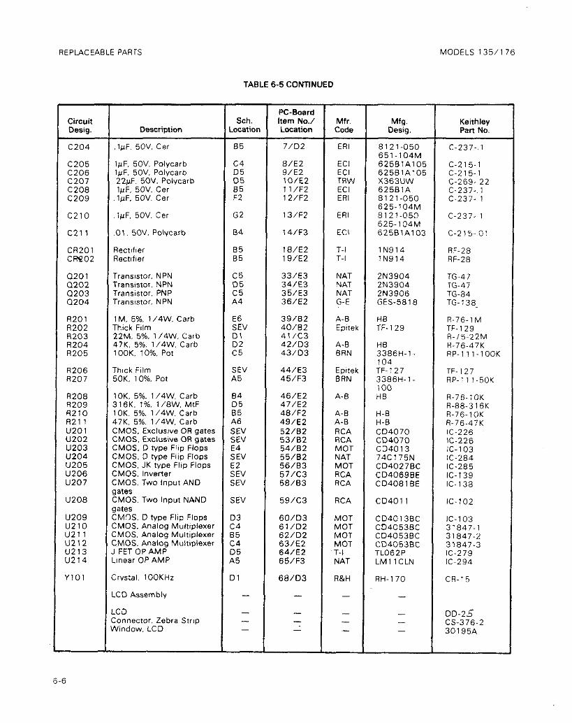
REPLACEABLE PARTS MODELS 135/l 76
TABLE 6-5 CONTINUED
Circuit Desig.
C204
c205 C206 c207 C208 c209
c210
c211
CA201 CR!202
0201 Q202 Q203 a204
R201 R202
E2 R205
R206 R207
R208 R209 R210 R21 1 u201 u202 U203 u204 U205 U206 U207
U208
u209 u210 u211 u212 u213 U214
YlOl
.lpF. 50V. Cer
1pF. 50V. Polycarb 1uF. 50V. Polycarb ~22pF. 50V. Polycarb ,lpF. 50V. Cer .lpF. 5OV. Cer
~1uF. 50V. Cer
.Ol, 50V. Polycarb
Rectlfler Rectlfiel
Trans,stor. NPN Transistor. NPN Transistor. PNP Transistor. NPN
1 M. 5%. 1/4W. Carb Thick Film 22M. 5%. 1/4W. Carb 47K. 5%. 1/4W. Carb lOOK. 10%. Pot
Thfck Film 50K. 10%. Pot
1 OK, 5%. 1/4W. Carb 316K. 1%. 1/8W. MtF 1 OK. 5%. 1/4W. Carb 47K. 5%. 1/4W. Carb CMOS. Exclusive OR gates CMOS, Exclusive OR gates CMOS. D type Fl!p Flops CMOS. 0 type Flip Flops CMOS. JK type Flip Flops CMOS. lnverter CMOS. Two Input AND gates CMOS. Two Input NAND gates CM%. D type Flip Flops CMOS, Analog Multiplexer CMOS. Analog Multiplexer CMOS. Analog Multiplexer , FET OP AMP Linear OP AMP
Irvstal. 1OOKHz
-CD Assembly
-CD :onnector. Zebra Strip Nindow. LCD
Sch. .ocation
65
c4
;z 85 F2
G2
84
85 Et5
c5 D5 c5 44
E6 SEV Dl D2 c5
SEV 45
34 35 35 46 ;f?J ;EV i4 jEV iz jEV ;EV
jEV
13 :4 15 :4 15 r5
)l
-
- - -
PC-Board Item No./ LOCatiOn
7/D2
8/E2 9/E2 lo/E2 ll/FZ 1 Z/F2
13/F2
14/F3
ltl/EZ 19/E2
33/E3 34/E3 35/E3 36/E2~
39/82 40/82 41/c3 42/D3 43103
44/E3 45/F3
46/E2 47/E2 48/F2 49/E2 52/82 53/02 54/B2 55/82 56/63 57/c3 58/B3
59/c3
60/D3 61/02 62/D2 63/E2 64/E2 65/F3
68/D3
-
-
7 -
Mfr. Code
ERI
ECI ECI TRW ECI ERI
ERI
ECI
8121-050 651.104M 62581~105 625BlA105 X363UW 625BlA 8121-050 625.104M 8121-050 625.104M 625BlA103
T-i T-l
lN914 lN914
NAT 2N3904 NAT 2N3904 NAT 2N3906 G-E GES-5818
A-B Epttek
HB TF-129
A-B BRN
Epitek BRN
A-B
HB 3386H-1.. 104
TF-127 3386H-1. 100 HB
A-B A-B RCA RCA MOT NAT MOT RCA RCA
H-B H-B CD4070 CD4070 CD4013 74C175N CD4027BC CD4069BE CD4081 BE
RCA CD401 1
MOT MOT MOT MOT T-l NAT
CD401 3BC CD4053BC CD4053BC CD4053BC TL062P LMllCLN
R&H
-
- - -
RH-170
-
- - -
Mfg. Desig
Keithley Part No.
C-237-,1
C-215-1 c-215-1 C-269-.22 C-237-.1 C-237. 1
C-237. 1
c-215-~01
RF-28 RF-28
TG-47 TG-47 TG-84 TG- 138
R-76.1M TF-129 R-76.22M R-76.47K RP-1 1 l-100K
TF- 127 RP-1 1 l-50K
R-76.10K R-88-3 16K R-76.10K R-76.47K (C-226 IC-226 IC-103 IC-284 IC-285 r-139 IC-138
IC- 102
IC-103 31847-l 31847-Z 31847.3 IC-279 lC~294
CA-1 5
DD-25 CS-376.2 30195A
6-6

MODELS 135,176 REPLACEABLE PARTS
TABLE 6-5 CONTINUED
Circuir D&g. Description
PC-&i Sch. Item NI
Location Locaric.. ____ -““, J, I
r
BAlOl
Cl01
Cl02 Cl03 Cl04 Cl05 Cl06 Cl07
Cl08
Cl09 Cl10
3111
3112
3113 :114 3115 3116 3117 3118 3119
:120 :121 :122 :t7101 IR102 :R103 :I?104 :fl105 ZR106 :ri107 :RloE ZR109 :Rllo
1101
1101
I101 1102
1103 1104 1105
I Gasket
I I
-
SUDDOit. LCD -
Ta0e
25OuF. 25V. Alum
1 OuF. 16V. Alum 1 OluF. 16V. Alum 1 OuF. 16V. Alum 1 OuF. 16V. Alum 1 O@F. 16V. Alum 4,7uF. 25V. Alum
1uF. 5OV. Cer
1 O!JF. 16V. Alum 1uF. 50V. Cer
1uF. 5OV. Cer El
1 op. 5ov. Cer El
1 OuF. 16V. Alum Z?OOP. 5oov. Cer D 5~. 1 OOOV. Cer D 15op. I ooov. Cer D 1 OpF. 16V. Alum 1 OuF. 16V. Alum O&F. 500V. Cer D
83 El El El Dl 01 Cl
~OlpF. 50V. Polycarb ,5P to 1 ZIP. 2ooov 1 50. 5ov. Cer D Recttfier Recftfter ReCtltler R.?ct,f,er Rectifier Aecrifier Recftfier Rect,f,er Rectlfler Low Voltage Reference lzenerl
75A. Fuse. 250V Max
Transistor. NPN
Thfck Film 200R. 10%. 3/4w. Pot
2.15K. 1%. l/lOW. MtF 8.98K. 1%. l/lOW. MtF Thtck Film
-
G2
G2
G2 G2 G2 G2 Gl Fl
Fl
63 El
A5 62 62 G2 G2 H2 Dl Cl El El A3 A3 Fl
A3
83
SEV Fl
Fl F2 SEV
3182
4/B2 5/B2 6/B2 7/B2 E/82 g/c2
lO/B3
11183 i 2/A3
13/A3
14/B4
15/B3 16/C3 17/B4 18185 19/B4 2O/B4 21184
22/86 23/C2 24/C2 27/B2 28/82 29/A3 3O/B4 31/B4 32184 33/84 34/B5 35/B5 36/C2
56/C2
60/82 61/C2
62/C2 63/C2 64/83
RIG
NIC NIC NIC NIC NIC NIC
ERI
NIC ERI
ERI
NIC
CLB CLB NIC NIC ERI
ECI EFJ CLB T-l T-l MOT T-I T-l T-i T-I MOT MOT MOT
L-F
NAT
Epltek BRN
ACI AC Eplrek
-
HC-4B-250 25.8P lGU,AlODT 16ULAlODT 16ULAlODT 16ULAlODT 16UlAlODT 25UlA4 R7D-T 8121.050 625.104M 16ULAlODT 8121-050 625.104M 8121-050 625.104~ SRlSIA 1 OOKAa 16UlA10DT
DD-050 DD-151 lGKU61ODK 16KUElODK 8 1 I -OOO- z5u 62581~103 273~1.1 DTZlA5 lN914 lN914 1 N4006 IN914 lN914 IN914 lN914 I N4006 1 N4006 LM385Z
312 750
2N3904
TF-127 3006P- 1 201 CR CR TF~l3,
30382A
EA. 14
C-314-250
c-313-x C.313~!L, C.313~12 c-313.;o c-313-10 c-314-4 7
C-237. !
c-313-10 C-237. 1
C-237. ?
C-237-100
c-313.16 c-22-2ioo~ C-64-50 C-64-130~ C-321-10 C-321-10 C-316-02
C-215~01 C-183-1 50 c-291-1 50 RF-28 RF-28 RF-38 RF-28 RF-28 RF-28 RF-28 RF-38 RF-38 30985A
FU-14
TG-47
TF-:28 RP-89-200
R-263~2 15K A-263~8 98K TF-131

REPLACEABLE PARTS
TABLE 6-5 CONTINUED
MODELS 135/176
Circuit Desig. Description
Sch. Location
PC-Board Item No./ Location
Mfr. Mfg. Code Desig.
Keithley Part No.
RI06 3.3K. 5%. 1/4W. Carb El 65184 A-B CE R107 21.93K. .l%. 1/6W. MfF El 66/B4 I7108 9.96K. .l%. 1/6W. MtF El 67104 ACI CR RlOS 2oo~.ilo%. Pot 01 68/65 ERN 3366H.l-
201 RllO 1 OOK. 10%. 1 W. Carb Cl 69/B5 A-B CE Rlll 1 OOK. 10%. Pot D2 70/85 BRN 3386H-l-l
104 Rl12 9.99. 1%. 1/8W. MtF A3 71/B5 ACI CR R113 50K. 10%. Pot 82 72/B5 BRN 3386~.i-
103 R114 .01a .5%. lW.Ww A2 73185 DLE R115 470K. 10%. 1W. Carb A5 74/06 IRC GB; W R116 Thick Film SEV 75/C2 CAD TF-126 R117 ’ 1%. 1 /BW. MtF F’ 76/C, - -
*Part of a set selected at the factory. (30985A) (The set includes CR1 10 and RI 17.)
fl-76-3.3~ R-179.21.93K Rl-79-S.SBK RP-1 1 l-200
R-2-100K RP-1 11-IOOK
R-179-9.99 RP-1 1 I-50K
R-280-.01 A-2-470K TF-126 R-88-’
RTlOl A4 78/B3 RT-7
SlOl Switch HZ 80/A2 CNW - s102
SW-41 7 Switch. Rotary SEV Bl/C3 CLB -
s103 SW-432
Switch. Rotary SEV 82/C4 CLB - SW-433
UlOl LCD. Counter G3 84/B 1 INT ICML7224 u102 CMOS. Low PowerOPAMP
IC-286 Fl 85/62 INT ICL7621
u103 CMOS. Voltage Converter IC-286
G2 86182 INT ICL766OCPA IC-287 u104 Linear OP AMP El B7/B4 NAT LM308 c-99 u105 JFET OP AMP Dl BE/B4 T-l TLOGlCP IC-227
- Test Lead Kit - - - - CA-B
Cover. Eatterv - - - - Cover. Fuse
30186C - - - - 30187C
6-8

MODELS 1351176 REPLACEABLE PARTS

REPLACEABLE PARTS MODELS 1351176

MODELS 1351176 REPLACEABLE PARTS

REPLACEABLE PARTS MODELS 135/176
6-12

MODELS 1351176 REPLACEABLE PARTS

REPLACEABLE PARTS MODELS 135/176
:
P t
t-7 I
6-14

,
\,
~.,)
‘X :
-CD, 1