Semimetal/Semiconductor Nanocomposites for Thermoelectrics
7
© 2011 WILEY-VCH Verlag GmbH & Co. KGaA, Weinheim 2377 www.advmat.de www.MaterialsViews.com RESEARCH NEWS wileyonlinelibrary.com Adv. Mater. 2011, 23, 2377–2383 Hong Lu,* Peter G. Burke, Arthur C. Gossard, Gehong Zeng, Ashok T. Ramu, Je-Hyeong Bahk, and John E. Bowers Semimetal/Semiconductor Nanocomposites for Thermoelectrics Dr. H. Lu, P. G. Burke, Prof. A. C. Gossard Materials Department University of California Santa Barbara, CA 93106–5050, USA E-mail: [email protected] Dr. G. Zeng, Dr. A. T. Ramu, Dr. J.-H. Bahk, Prof. J. E. Bowers Department of Electrical and Computer Engineering University of California Santa Barbara, CA 93106–9560, USA DOI: 10.1002/adma.201100449 1. Introduction Thermoelectrics, [1] a technology for direct thermal to electrical energy conversion, has attracted more and more attention recently as an alternative source of renewable energy. There are a large variety of thermoelectric materials, mostly studied in bulk form, such as skutterudites, clathrates, and Zintl phases, etc, that have been explored for higher thermoelectric effi- ciency. [2,3] Thermoelectric materials are normally evaluated by the dimensionless figure of merit ZT and ZT = S 2 σT/ κ, where S is the Seebeck coefficient, σ is the electrical conductivity, T is the absolute temperature, and κ is the thermal conductivity. A good thermoelectric material should have high electrical con- ductivity to minimize Joule heating, low thermal conductivity to prevent thermal shorting and a high Seebeck coefficient to maximize the conversion of heat to electrical power. Engi- neering materials into or with nanostructures, [4–6] can result in significant improvement in the thermoelectric figure of merit, [7–9] often beyond the best available in bulk materials. We have focused on utilizing nanostructures of rare earth-V (RE-V) compounds in order to engineer III-V semiconductors with enhanced thermo- electric properties. This can enable easy integration of thermoelectric devices with the current advanced electronic and pho- tonic devices based on III-V semiconduc- tors, for waste heat recovery, temperature stabilization, or integrated cooling. [10,11] The thermoelectric figure of merit of these III-V nanocomposites has monotonically increased with temperature all the way up to 800 K. [12] This makes these materials especially suitable for integration into seg- mented thermoelectric devices that work with large temperature gradients. In the following, different III-V nanocomposites will be discussed, and enhancements in both material properties and device per- formance will be shown. 2. RE-V/III-V Nanocomposites 2.1. ErAs:InGaAlAs Nanocomposites (Lattice-Matched to InP Substrate) The first material system that was systematically explored in our work to improve thermoelectric properties was ErAs:InGaAlAs nanocomposites grown lattice matched to InP substrates. We started the studies on ErAs:InGaAlAs nanocomposites made of a superlattice structure, having alternating ErAs and InGaAlAs layers. In this structure, the ErAs deposition could be varied but not up to a full surface coverage to ensure high quality InGaAlAs overgrowth. Enhanced Seebeck coefficient and elec- tron filtering were observed and demonstrated on this material system. [13] Later, more focus was put into ErAs:InGaAlAs nano- composites grown by a codeposition process. Nanoparticles of ErAs are formed spontaneously within the III-V semiconductor matrix during the codeposition when the solubility limit is exceeded. [14] This material design in many ways is preferable because the numerous shutter operations required for superlat- tice structures can be eliminated, which is significant for the growth of thick layers required for power generator module fab- rication. In addition, the Schottky barriers formed at the inter- faces between these randomly distributed ErAs nanoparticles and the InGaAlAs matrix can behave as non-planar electron filters. [13,15] These semimetallic ErAs nanoparticles, normally having a diameter of about 3 nm in InGaAlAs, can contribute electrons to the semiconductor matrix to improve the electrical In this work, we present research on semimetal-semiconductor nanocom- posites grown by molecular beam epitaxy (MBE) for thermoelectric appli- cations. We study several different III-V semiconductors embedded with semimetallic rare earth-group V (RE-V) compounds, but focus is given here to ErSb:In x Ga 1−x Sb as a promising p-type thermoelectric material. Nano- structures of RE-V compounds are formed and embedded within the III-V semiconductor matrix. By codoping the nanocomposites with the appropriate dopants, both n-type and p-type materials have been made for thermoelec- tric applications. The thermoelectric properties have been engineered for enhanced thermoelectric device performance. Segmented thermoelectric power generator modules using 50 μm thick Er-containing nanocomposites have been fabricated and measured. Research on different rare earth ele- ments for thermoelectrics is discussed.
Transcript of Semimetal/Semiconductor Nanocomposites for Thermoelectrics
www.advmat.dewww.MaterialsViews.com
RES
EARCH N
EW
Hong Lu , * Peter G. Burke , Arthur C. Gossard , Gehong Zeng , Ashok T. Ramu , Je-Hyeong Bahk , and John E. Bowers
Semimetal/Semiconductor Nanocomposites for Thermoelectrics
S
In this work, we present research on semimetal-semiconductor nanocom-posites grown by molecular beam epitaxy (MBE) for thermoelectric appli-cations. We study several different III-V semiconductors embedded with semimetallic rare earth-group V (RE-V) compounds, but focus is given here to ErSb:In x Ga 1−x Sb as a promising p-type thermoelectric material. Nano-structures of RE-V compounds are formed and embedded within the III-V semiconductor matrix. By codoping the nanocomposites with the appropriate dopants, both n-type and p-type materials have been made for thermoelec-tric applications. The thermoelectric properties have been engineered for enhanced thermoelectric device performance. Segmented thermoelectric power generator modules using 50 μ m thick Er-containing nanocomposites have been fabricated and measured. Research on different rare earth ele-ments for thermoelectrics is discussed.
1. Introduction
Thermoelectrics, [ 1 ] a technology for direct thermal to electrical energy conversion, has attracted more and more attention recently as an alternative source of renewable energy. There are a large variety of thermoelectric materials, mostly studied in bulk form, such as skutterudites, clathrates, and Zintl phases, etc, that have been explored for higher thermoelectric effi -ciency. [ 2 , 3 ] Thermoelectric materials are normally evaluated by the dimensionless fi gure of merit ZT and ZT = S 2 σ T/ κ , where S is the Seebeck coeffi cient, σ is the electrical conductivity, T is the absolute temperature, and κ is the thermal conductivity. A good thermoelectric material should have high electrical con-ductivity to minimize Joule heating, low thermal conductivity to prevent thermal shorting and a high Seebeck coeffi cient to maximize the conversion of heat to electrical power. Engi-neering materials into or with nanostructures, [ 4–6 ] can result in signifi cant improvement in the thermoelectric fi gure of merit, [ 7–9 ] often beyond the best available in bulk materials. We have focused on utilizing nanostructures of rare earth-V (RE-V)
© 2011 WILEY-VCH Verlag GmbH & Co. KGaA, WeinheimAdv. Mater. 2011, 23, 2377–2383
Dr. H. Lu , P. G. Burke , Prof. A. C. Gossard Materials DepartmentUniversity of CaliforniaSanta Barbara, CA 93106–5050, USA E-mail: [email protected] Dr. G. Zeng , Dr. A. T. Ramu , Dr. J.-H. Bahk , Prof. J. E. Bowers Department of Electrical and Computer EngineeringUniversity of CaliforniaSanta Barbara, CA 93106–9560, USA
DOI: 10.1002/adma.201100449
compounds in order to engineer III-V semiconductors with enhanced thermo-electric properties. This can enable easy integration of thermoelectric devices with the current advanced electronic and pho-tonic devices based on III-V semiconduc-tors, for waste heat recovery, temperature stabilization, or integrated cooling. [ 10 , 11 ] The thermoelectric fi gure of merit of these III-V nanocomposites has monotonically increased with temperature all the way up to 800 K. [ 12 ] This makes these materials especially suitable for integration into seg-mented thermoelectric devices that work with large temperature gradients. In the following, different III-V nanocomposites will be discussed, and enhancements in both material properties and device per-formance will be shown.
2. RE-V/III-V Nanocomposites
2.1. ErAs:InGaAlAs Nanocomposites (Lattice-Matched to InP Substrate)
The fi rst material system that was systematically explored in our work to improve thermoelectric properties was ErAs:InGaAlAs nanocomposites grown lattice matched to InP substrates. We started the studies on ErAs:InGaAlAs nanocomposites made of a superlattice structure, having alternating ErAs and InGaAlAs layers. In this structure, the ErAs deposition could be varied but not up to a full surface coverage to ensure high quality InGaAlAs overgrowth. Enhanced Seebeck coeffi cient and elec-tron fi ltering were observed and demonstrated on this material system. [ 13 ] Later, more focus was put into ErAs:InGaAlAs nano-composites grown by a codeposition process. Nanoparticles of ErAs are formed spontaneously within the III-V semiconductor matrix during the codeposition when the solubility limit is exceeded. [ 14 ] This material design in many ways is preferable because the numerous shutter operations required for superlat-tice structures can be eliminated, which is signifi cant for the growth of thick layers required for power generator module fab-rication. In addition, the Schottky barriers formed at the inter-faces between these randomly distributed ErAs nanoparticles and the InGaAlAs matrix can behave as non-planar electron fi lters. [ 13 , 15 ] These semimetallic ErAs nanoparticles, normally having a diameter of about 3 nm in InGaAlAs, can contribute electrons to the semiconductor matrix to improve the electrical
2377wileyonlinelibrary.com
2378
www.advmat.dewww.MaterialsViews.com
RES
EARCH N
EWS
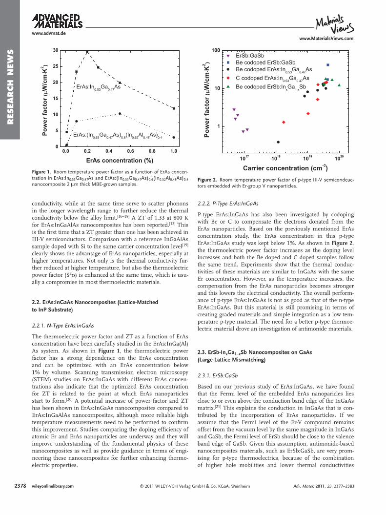
Figure 1 . Room temperature power factor as a function of ErAs concen-tration in ErAs:In 0.53 Ga 0.47 As and ErAs:(In 0.53 Ga 0.47 As) 0.6 (In 0.52 Al 0.48 As) 0.4 nanocomposite 2 μ m thick MBE-grown samples.
Figure 2 . Room temperature power factor of p-type III-V semicondcuc-tors embedded with Er-group V nanoparticles.
conductivity, while at the same time serve to scatter phonons in the longer wavelength range to further reduce the thermal conductivity below the alloy limit. [ 16–18 ] A ZT of 1.33 at 800 K for ErAs:InGaAlAs nanocomposites has been reported. [ 12 ] This is the fi rst time that a ZT greater than one has been achieved in III-V semiconductors. Comparison with a reference InGaAlAs sample doped with Si to the same carrier concentration level [ 19 ] clearly shows the advantage of ErAs nanoparticles, especially at higher temperatures. Not only is the thermal conductivity fur-ther reduced at higher temperature, but also the thermoelectric power factor (S 2 σ ) is enhanced at the same time, which is usu-ally a compromise in most thermoelectric materials.
2.2. ErAs:InGaAs Nanocomposites (Lattice-Matched to InP Substrate)
2.2.1. N-Type ErAs:InGaAs
The thermoelectric power factor and ZT as a function of ErAs concentration have been carefully studied in the ErAs:InGa(Al)As system. As shown in Figure 1 , the thermoelectric power factor has a strong dependence on the ErAs concentration and can be optimized with an ErAs concentration below 1% by volume. Scanning transmission electron microscopy (STEM) studies on ErAs:InGaAs with different ErAs concen-trations also indicate that the optimized ErAs concentration for ZT is related to the point at which ErAs nanoparticles start to form. [ 20 ] A potential increase of power factor and ZT has been shown in ErAs:InGaAs nanocomposites compared to ErAs:InGaAlAs nanocomposites, although more reliable high temperature measurements need to be performed to confi rm this improvement. Studies comparing the doping effi ciency of atomic Er and ErAs nanoparticles are underway and they will improve understanding of the fundamental physics of these nanocomposites as well as provide guidance in terms of engi-neering these nanocomposites for further enhancing thermo-electric properties.
© 2011 WILEY-VCH Verlag Gwileyonlinelibrary.com
2.2.2. P-Type ErAs:InGaAs
P-type ErAs:InGaAs has also been investigated by codoping with Be or C to compensate the electrons donated from the ErAs nanoparticles. Based on the previously mentioned ErAs concentration study, the ErAs concentration in this p-type ErAs:InGaAs study was kept below 1%. As shown in Figure 2 , the thermoelectric power factor increases as the doping level increases and both the Be doped and C doped samples follow the same trend. Experiments show that the thermal conduc-tivities of these materials are similar to InGaAs with the same Er concentration. However, as the temperature increases, the compensation from the ErAs nanoparticles becomes stronger and this lowers the electrical conductivity. The overall perform-ance of p-type ErAs:InGaAs is not as good as that of the n-type ErAs:InGaAs. But this material is still promising in terms of creating graded materials and simple integration as a low tem-perature p-type material. The need for a better p-type thermoe-lectric material drove an investigation of antimonide materials.
2.3. ErSb-In x Ga 1−x Sb Nanocomposites on GaAs (Large Lattice Mismatching)
2.3.1. ErSb:GaSb
Based on our previous study of ErAs:InGaAs, we have found that the Fermi level of the embedded ErAs nanoparicles lies close to or even above the conduction band edge of the InGaAs matrix. [ 21 ] This explains the conduction in InGaAs that is con-tributed by the incorporation of ErAs nanoparticles. If we assume that the Fermi level of the Er-V compound remains offset from the vacuum level by the same magnitude in InGaAs and GaSb, the Fermi level of ErSb should be close to the valence band edge of GaSb. Given this assumption, antimonide-based nanocomposites materials, such as ErSb:GaSb, are very prom-ising for p-type thermoelectrics, because of the combination of higher hole mobilities and lower thermal conductivities
mbH & Co. KGaA, Weinheim Adv. Mater. 2011, 23, 2377–2383

www.advmat.dewww.MaterialsViews.com
RES
EARCH N
EWS
Figure 3 . Temperature dependent (a) thermal conductivity measured by the 3 ω method and (b) ZT of p-type ErSb:In x Ga 1−x Sb with 12% and 28% In composition.
compared to the corresponding arsenides. We have investigated the MBE growth of these nanocomposites by using homoepi-taxial substrates and buffers for better growth control and opti-mization of growth conditions. Epitaxial fi lms of ErSb:GaSb and ErSb:InSb have been grown on GaSb and InSb substrates, respectively. Similar to the ErAs:InGaAs material system, ErSb nanoparticles are formed spontaneously during a codeposition process within the GaSb matrix. However, these substrates are intrinsically conductive which makes it diffi cult to measure the electrical and thermal properties of the epitaxial fi lms due to the substrate conductivity. Therefore, many efforts have been put into the heteroepitaxial growth on different substrates such as GaAs, which has a lattice mismatch of 7.8% between GaSb and GaAs.
A series of ErSb:GaSb samples have been grown on semi-insulating GaAs substrates and characterized. The hole con-centration of the material is increased by the incorporation of Er, which proves that the Fermi level of Er is close to the valence band edge of GaSb as qualitatively expected from the band alignments. However, the overall carrier density is still low with only Er doping, and the power factor of ErSb:GaSb samples is one order of magnitude lower than the p-type ErAs:InGaAs samples. Therefore, we have doped the GaSb with Be or C to increase the carrier density. The resulting best room temperature power factor of Be doped GaSb is ∼ 28 μ W/cm · K 2 . To reduce the thermal conductivity of Be doped GaSb, we code-posited Er during the growth, forming embedded ErSb nano-particles which scatter phonons. Two ErSb:GaSb samples with different Er concentrations and codoped with 4 × 10 19 cm − 3 Be were grown and the room temperature power factors were measured as shown in Figure 2 as well. The best power factor ∼ 42 μ W/cm · K 2 is three times higher than the best p-type ErAs:InGaAs that we have grown.
The room temperature power factor shows the potential of ErSb:GaSb for a good p-type thermoelectric material, but fur-ther enhancement of ZT can be achieved by alloying GaSb with InSb to reduce thermal conductivity.
2.3.2. ErSb:In x Ga 1−x Sb Nanocomposites
The lattice mismatch between In x Ga 1−x Sb alloys and GaAs increases with more In incorporation. Good material quality has to be ensured before any electrical or thermal measure-ment is conducted. We have optimized the growth temperature, the growth rate, Sb/III ratio, and used a GaSb buffer layer to enhance the material quality. As observed by the X-ray diffrac-tion spectra we have succeeded in increasing the In composi-tion to as high as 73% without any second phase formation.
The room temperature power factor data of Be codoped ErSb:In x Ga 1–x Sb samples with different In compositions are also shown in Figure 2 for a comparison. The dependence of alloy thermal conductivity on In composition has been dem-onstrated by the thermal conductivity measurement shown in Figure 3 . The thermal conductivity of the sample with 28% In composition is clearly reduced by more than 30% at room temperature as compared to the sample with 12% In composi-tion (Figure 3 a). By comparing samples with and without ErSb nanoparticles, a reduction of thermal conductivity by nanopar-ticle scattering is also demonstrated for the samples with 28%
© 2011 WILEY-VCH Verlag GmAdv. Mater. 2011, 23, 2377–2383
In composition. Temperature dependent ZT (Figure 3 b) shows that ErSb:In x Ga 1−x Sb performs better with higher In composi-tion. Research is currently underway to further increase ZT by fi ne-tuning the alloy composition and optimizing the doping level.
3. Thick Material Growth by MBE
Thick material (50–100 μ m) is required for fabricating thermo-electric power generator modules. Thicker thermoelectric legs used in the device module can relax the requirements for the heat sink design and also for the metal/semiconductor contact resistance. Thick layer growth by MBE for thermoelectric appli-cations was initially demonstrated by Harman et al. [ 22 ] It is a challenge in terms of controlling the lattice-matching condition and temperature uniformity across the substrate through a long time growth. In order to shorten the growth time, a 2 μ m/h growth rate has been used for thick layer growth. The material qualities of the thick layers grown by MBE have been improved
2379bH & Co. KGaA, Weinheim wileyonlinelibrary.com

2380
www.advmat.dewww.MaterialsViews.com
RES
EARCH N
EWS
Figure 4 . Measured Seebeck coeffi cient versus measured carrier (hole) concentration for undoped GaSb, Be doped GaSb and C doped GaSb samples. The calculated Seebeck coeffi cient of p-type GaSb, with details described by Ramu et al., [ 31 ] is plotted as a dashed line.
by carefully optimizing growth conditions. However, cracking and bowing are still the main problems as the sample thickness increases. The difference in the thermal expansion coeffi cient of the epi-fi lm and the substrate is the main reason why the sample cracks and bows. Additional stress is caused by sub-strate temperature non-uniformity, extra stress from the sample holder, and quick substrate cooling rates. In addition to these effects, we found that the grown sample always bows along one direction; this may be due to the orientation dependent surface mobility of atoms during growth. To reduce the possible extra stress and improve the temperature uniformity, we have tried different ways to mount the substrate wafer. Recently, we have succeeded in reducing bowing by indium bonding an entire 2-inch wafer, of either InP or GaAs, to a Mo backing plate for the long growth process ( > 40 h), and including a slow tem-perature ramping rate (1.0 ° C/min) during cooling down. Both n-type ErAs:InGaAs lattice matched to InP substrate and p-type ErSb:In 0.12 Ga 0.88 Sb lattice mismatched to GaAs substrate with a total thickness of 54 μ m have been grown without cracks as shown in Figure 5 a. In particular, this is the fi rst time that a thick layer of an epi-fi lm of antimonide is grown on a substrate with a mismatch higher than 8% by MBE. Both of these two samples have been used in segmented thermoelectric power generator modules as described below.
4. High Temperature Characterization and Modeling
4.1. Processing for High Temperature Measurement
Due to the fact that these Er-based III-V nanocomposites show their best potential at high temperatures, reliable high tempera-ture measurement is very important for optimization of mate-rial composition and device fabrication. Surface passivation of the III-V nanocomposites materials can eliminate the decom-position of the constituent materials at high temperature, there-fore ensuring the feasibility and reliability of high temperature measurements. All the samples for high temperature electrical conductivity and Seebeck coeffi cient measurements underwent the following process:
i Lithography and wet-etching to defi ne measurement mesas ii SiN x /SiO 2 200 nm/100 nm deposition by PECVD iii Lithography to defi ne the contact areas iv Buffered HF and CF 4 etch to etch through the passivation
layer and expose the semiconductor surface v Metal deposition using electron beam evaporation
Contact to n-type material was made using a Ti/Au (40/400 nm) metal stack, while contact to p-type material was made using a Pt/Ti/Pt/Au (2/17.5/17.5/400 nm) metal stack. Measurements were made under a vacuum of ∼ 1 × 10 − 4 torr. Temperature measurements were realized using type-K thermo-couples contacted to the sample surface. Good thermal contacts between the heat sources and the sample, as well as between the thermocouples and the sample, were enabled by a silver-based thermal compound. These procedures have been established on ErAs:InGaAlAs samples for high temperature characterization
© 2011 WILEY-VCH Verlag Gwileyonlinelibrary.com
previously and proved to be reliable up to 800 K. [ 12 , 23 , 24 ] How-ever, the substrate conduction starts to affect electrical meas-urements when the temperature is close to 300 ° C although the substrate is insulating at room temperature. For a more reli-able high temperature measurement, the substrate needs to be removed and the epitaxial fi lm needs to be transferred to an insulating wafer, such as sapphire. A device fabrication method based on oxide-oxide bonding has also been established on III-V nanocomposites grown on InP substrates. [ 23 ]
Temperature dependent thermal conductivity was measured using the 3 ω method. [ 25 ] More details of the measurements on our samples including the fabrication process, the experimental setup and the data analysis are described in Ref. [26]. Careful comparison of thermal conductivity results measured by the 3 ω method and the time-domain thermorefl ectance method has been reported and shows good agreement. [ 27 ]
4.2. High Temperature Measurement and Modeling
We have completed detailed theoretical and experimental studies of thermoelectric transport in ErAs:InGaAlAs nano-composites. [ 13 , 19 , 28 , 29 ] Alternative modeling methods are also explored to expand our understanding of this material system as well as apply it to other material systems. [ 30 ] Similar theo-retical work has been performed on p-type GaSb, both unin-tentionally doped and doped with shallow acceptors like Be and C. We have treated the effects of inter-band scattering and optical-mode phonon scattering using an extension of the iterative method developed earlier. [ 30 ] Without the use of fi t-ting or adjustable parameters, the results of the calculations [ 31 ] agree with experimental mobility data to within 20%, and with experimental Seebeck coeffi cient data to within 10%, across a wide range of hole concentrations (5 × 10 16 to 5 × 10 19 cm − 3 ) ( Figure 4 ) and temperatures (300–550 K). These calcula-tions helped establish appropriate controls for evaluating the
mbH & Co. KGaA, Weinheim Adv. Mater. 2011, 23, 2377–2383

www.advmat.dewww.MaterialsViews.com
RES
EARCH N
EWS
performance of various Er-based nanocomposites of GaSb and InGaSb. Nanoparticles reduce the hole mobility and hence the electrical conductivity, but quantitative studies of this effect are not conclusive because of the diffi culty of growing appropriate controls with exactly the same hole concentration. Further simulations on ErSb:In x Ga 1–x Sb considering both the ErSb nano-particles incorporation and the optimized doping level will be performed.
5. Segmented Power Generator Module Fabrication and Characterization
Solid-state thermoelectric power generator modules composed of n and p element couples can convert thermal energy to elec-trical energy directly by the Seebeck effect. Thermoelectric
Figure 5. (a) a 54 μm thick thermoelectric sample grown on a 2 inch substrate by MBE, and indium bonded to a Mo backing plate; (b) a quarter of a 2 inch 54 μm p-type ErSb:InGaSb sample after the GaAs substrate is removed; (c) 1.4 mm × 1.4 mm elements diced for bonding; (d) lower segment of n- and p-type Bi2Te3 array elements bonded on a DBC ceramic plate; (e) a completed 8 × 8 segmented generator module; (f) power output measured from the segmented model.
power generators are generally used in deep space missons and have shown reliability and durability as power sources. [ 32 ] The potential of thermoelectric power generators in pro-viding cleaner energy and reducing environ-mental impact has also been recognized. The energy conversion performance of a ther-moelectric power generator module [ 1 , 33 , 34 ] depends on the thermoelectric properties of the elements as well as the module’s working temperatures. A thermoelectric power gen-erator module is a heat engine, and thus its maximum possible effi ciency is given by the Carnot value, which is equal to Δ T/T h , where Δ T is the temperature difference across the element and T h is the hot side temperature. Therefore a large Δ T is desired for large output power and high effi ciency. Segmented thermoelectric materials can enhance the effi ciency of a thermoelectric power gener-ator. [ 35 , 36 ] Previously, we have demonstrated 16 × 16 element segmented generator mod-ules using ErAs:InGaAlAs as both the n- and p-legs. [ 37 , 38 ] To use the better performing ErSb:InGaSb for the fi rst time, segmented generator modules of 8 × 8 elements were designed with segmented elements of 50 μ m (active region) n-ErAs:InGaAs and p-ErSb:InGaSb on 0.8 mm Bi 2 Te 3. As the thickness of the element is increased, thermal parasitic loss is reduced, and the tempera-ture difference across the elements can be substantially increased. Each segment can work at its own optimum temperature range: n-ErAs:InGaAs and p-ErSb:InGaSb segment is at the hot side, and Bi 2 Te 3 at the cold side.
Thermal expansion is one of the major issues that cause the failure of thermoelectric modules working at larger temperature dif-ferences between the cold side and the hot side. To reduce this problem, AlN plates were used instead of alumina for their smaller linear thermal expansion. Also used was
© 2011 WILEY-VCH Verlag GAdv. Mater. 2011, 23, 2377–2383
Direct Bond Copper (DBC), a process where solid copper foil is bonded to an AlN plate at a high temperature in an inert atmosphere. The advantages of using DBC as bonding plates in our module are i) electrical conductivity 95% of pure Cu for the copper pads; ii) high metal-to-plate thermal conductivity for less thermal loss at the interface of the ceramic plate and the metal pads; iii) bonding pads can be patterned by standard IC processing and formed by wet-etching.
The contact metals were deposited on the front side of the samples: Ni/Ge/Au/Ni for n-type and Ti/Pd/Ti/Au for p-type. The InP substrate was removed by wet etching using an HCl solution, while the GaAs substrate was removed using an NH 4 OH:H 2 O 2 etchant. The GaAs substrate was fi rst polished mechanically and etched selectively using NH 4 OH:H 2 O 2 . After the substrate removal (as shown in Figure 5 b), the surface of the thin fi lm was coated with the same contact metals as those
2381mbH & Co. KGaA, Weinheim wileyonlinelibrary.com

238
www.advmat.dewww.MaterialsViews.com
RES
EARCH N
EWS
used on the front side surface. The 50 μ m thick fi lms, with bothsides deposited with contact metals, were diced into 1.4 mm × 1.4 mm square elements for bonding (Figure 5 c).
The lower segment of the module consists of 8 × 8 n-type Bi 2 Te 3 and p-type Bi 2 Te 3 array elements, which were bonded on the DBC ceramic plate using the pick-and-place method as shown in Figure 5 d. After the lower segment elements were bonded, 50 μ m n-ErAs:InGaAs and p-ErSb:InGaSb ele-ments were bonded to the top of the n- and p-type Bi 2 Te 3 ele-ments, respectively. Then, the upper and lower ceramic plates were bonded together to form a segmented element generator module as shown in Figure 5 e.
The segmented module was characterized using our module measurement setup consisting of a heat source, a heat sink with cooling water set to 285 K and a computer controlled data acquisition system. An output power over 1.4 W was measured at impedance match conditions when the heat source tempera-ture was increased to around 300 ° C (Figure 5 f).
6. Other Rare Earth for Thermoelectrics
Different rare-earth elements other than Er are interesting and Sc and Tb have been studied recently by the Palmstrøm group at UCSB [ 39 ] and the Zide group at the University of Delaware, [ 40 ] respectively.
Scandium is the smallest rare earth element and the solu-bility limit of Sc in III-Vs is likely to be different from that of Er. The small lattice spacing and density of Sc-V compounds [ 41 ] and the possibly different particle sizes of the Sc-V compounds relative to other RE-V compounds can alter the thermal con-ductivity reduction due to the scattering of phonons with a different wavelength. In general, the electrical properties of ScAs:InGaAs are similar to those of ErAs:InGaAs. [ 39 ] Further study on using Sc-V together with other RE-V (e.g., ErAs) to engineer the thermoelectric properties of III-V semiconductors is being conducted at UCSB.
Efforts by the Zide group to incorporate Tb-V compounds into InGaAs and GaAs have shown that metallic nanostructures are formed during codeposition by MBE. [ 40 ] About 10% TbAs incorporation has lowered the thermal conductivity of GaAs by a factor of 4 at room temperature. The different properties of Tb-based nanocomposites relative to Er-based nanocomposites makes the Tb containing arsenides interesting for fundamental material studies as well as for thermoelectric applications.
7. Conclusions
We have shown that using Er can greatly improve the thermo-electric properties of III-V semiconductors, especially at higher temperatures. The concept of phonon scattering by Er-V nanopar-ticles to reduce the thermal conductivity below the alloy limit has been demonstrated in different III-V nanocomposites. The sem-imetallic properties of RE-V compounds can be used to improve the electrical conductivity in a host semiconductor and the See-beck coeffi cient can be improved by engineering the Schottky barrier formed at the interface of the semimetal and semicon-ductor. The MBE growth of this semimetal-semiconductor
2 © 2011 WILEY-VCH Verlag Gwileyonlinelibrary.com
material system, even with a larger thickness than a normal MBE grown epitaxial layer, has been well established, including formation of epitaxial fi lms up to 60 μ m thick. More studies are still underway and more exciting phenomena and promising results are expected. The big advantage of working on these semimetal-semiconductor nanocomposites for thermoelectrics is not solely to obtain a higher ZT, but to demonstrate the capa-bility of engineering traditional semiconductors for enhanced thermoelectric performance in both materials and devices and integrate them with electronic and photonic devices.
Acknowledgements The authors would like to thank Dr. Chris Palmstrøm and Dr. Ali Shakouri for useful discussions, and Dr. Dongyan Xu for the thermal conductivity measurement performed at University of California, Berkeley. This work has been fi nancially supported by the Offi ce of Naval Research, primarily through the TEC-MURI program, and by the DARPA NMP program as well as the Center for Energy Effi cient Materials (CEEM), an Energy Frontier Research Center (EFRC) funded at UCSB by the DOE Offi ce of Basic Energy Sciences. This article is part of the Special Issue on Materials Research at the University of California, Santa Barbara.
Received: February 4, 2011 Published online: April 15, 2011
[ 1 ] D. M. Rowe , CRC Handbook of Thermoelectrics , CRC Press 1995 . [ 2 ] G. S. Nolas , J. Poon , M. Kanatzidis , MRS Bulletin 2006 , 31 , 199 . [ 3 ] G. J. Snyder , E.S. Toberer , Nature Materials 2008 , 7 , 105 . [ 4 ] M. S. Dresselhaus , G. Chen , M. Y. Tang , R. G. Yang , H. Lee ,
D. Z. Wang , Z. F. Ren , J.-P. Fleurial , P. Gogna , Advanced Materials 2007 , 19 , 1043 .
[ 5 ] C. J. Vineis , A. Shakouri , A. Majumdar , M. G. Kanatzidis , Advanced Materials 2010 , 22 , 3970 .
[ 6 ] S. K. Bux , J.-P. Fleurial , R. B. Kaner , Chemical Communications 2010 , 46 , 8311 .
[ 7 ] L. D. Hicks , M. S. Dresselhaus , Phys. Rev. B 1993 , 47 , 12 727 . [ 8 ] A. Majumdar , Science 2004 , 303 , 777 . [ 9 ] S. V. Faleev , F. Léonard , Phys. Rev. B 2008 , 77 , 214304 . [ 10 ] L.E. Bell , Science 2008 , 321 , 1457 . [ 11 ] H. J. Goldsmid , Electronic Refrigeration , Pion Ltd. , London 1986 . [ 12 ] J. M. O. Zide , J.-H. Bahk , R. Singh , M. Zebarjadi , G. Zeng , H. Lu ,
J. P. Feser , D. Xu , S. L. Singer , Z. X. Bian , A. Majumdar , J. E. Bowers , A. Shakouri , a C. Gossard , J. Appl. Phys. 2010 , 108 , 123702 .
[ 13 ] J. M. O. Zide , D. Vashaee , Z. Bian , G. Zeng , J. E. Bowers , A. Shakouri , A. C. Gossard , Phys. Rev. B 2006 , 74 , 205335 .
[ 14 ] D. O. Klenov , D. C. Driscoll , A. C. Gossard , S. Stemmer , Appl. Phys. Lett. 2005 , 86 , 1912 .
[ 15 ] J. M. O. Zide , Molecular Beam Epitaxial Growth of III-V semi-metal/III-V Semiconductor Nanocomposites For Energy Conversion Applications 2007 .
[ 16 ] J. M. O. Zide , D. O. Klenov , S. Stemmer , A. C. Gossard , G. Zeng , J. E. Bowers , D. Vashaee , A. Shakouri , Appl. Phys. Lett. 2005 , 87 , 112102 .
[ 17 ] W. Kim , J. M. O. Zide , A. C. Gossard , D. O. Klenov , S. Stemmer , A. Shakouri , A. Majumdar , Phys. Rev. Lett. 2006 , 96 , 45901 .
[ 18 ] W. Kim , S. L. Singer , A. Majumdar , J. M. O. Zide , D. Klenov , A. C. Gossard , S. Stemmer , Nano Lett. 2008 , 8 , 2097 .
[ 19 ] J.-H. Bahk , Z. Bian , M. Zebarjadi , J. M. O. Zide , H. Lu , D. Xu , J. P. Feser , G. Zeng , A. Majumdar , A. C. Gossard , A. Shakouri , J. E. Bowers , Phys. Rev. B 2010 , 81 , 235209 .
[ 20 ] P. G. Burke , H. Lu , N. G. Rudawski , S. Stemmer , A. C. Gossard , J.-H. Bahk , J. E. Bowers , J. Vac. Sci. Technol., B 2011 , 29 , 03C117 .
mbH & Co. KGaA, Weinheim Adv. Mater. 2011, 23, 2377–2383
www.advmat.dewww.MaterialsViews.com
RES
EARCH N
EWS
[ 21 ] D. C. Driscoll , M. P. Hanson , C. Kadow , A. C. Gossard , Appl. Phys. Lett. 2001 , 78 , 1703 .
[ 22 ] T.C. Harman , P. J. Taylor , M. P. Walsh , B. E. LaForge , Science 2002 , 297 , 2229 .
[ 23 ] J.-H. Bahk , G. Zeng , J. M. O. Zide , H. Lu , R. Singh , D. Liang , A. T. Ramu , P. Burke , Z. Bian , A. C. Gossard , A. Shakouri , J. E. Bowers , J. Electron. Mater. 2010 , 39 , 1125 .
[ 24 ] J.-H. Bahk , Electron Transport In ErAs:InGa(Al)As Metal/Semi-conductor Nanocomposites 2010 .
[ 25 ] D. G. Cahill , Rev. Sci. Instrum. 1990 , 61 , 802 . [ 26 ] W. C. Kim , Thermal Transport in Nanostructure Materials 2005 . [ 27 ] Y. K. Koh , S. L. Singer , W. Kim , J. M. O. Zide , H. Lu , D. G. Cahill ,
A. Majumdar , A. C. Gossard , J. Appl. Phys. 2009 , 105 , 054303 . [ 28 ] D. Vashaee , Y. Zhang , A. Shakouri , G. Zeng , Y.-J. Chiu , Phys. Rev. B
2006 , 74 . 195315 . [ 29 ] M. Zebarjadi , K. Esfarjani , A. Shakouri , J.-H. Bahk , Z. X. Bian ,
G. Zeng , J. E. Bowers , H. Lu , J. M. O. Zide , A. C. Gossard , App. Phys. Letters 2009 , 94 , 202105 .
[ 30 ] A. T. Ramu , L. E. Cassels , N. H. Hackman , H. Lu , J. M. O. Zide , J. E. Bowers , J. Appl. Phys. 2010 , 107 , 083707 .
[ 31 ] A. T. Ramu , L. E. Cassels , N. H. Hackman , H. Lu , J.M.O. Zide , J. E. Bowers , J. Appl. Phys. 2011 , 109 , 033704 .
© 2011 WILEY-VCH Verlag GAdv. Mater. 2011, 23, 2377–2383
[ 32 ] C. Wood , Rep. Prog. Phys. 1988 , 51 , 459 – 539 . [ 33 ] T. C. Harman , J. M. Honig , Thermoelectric and Thermomagnetic
Effects and Applications , McGraw-Hill , New York, NY 1967 . [ 34 ] R. R. Heikes , R. W. Ure , Thermoelectricity: Science and Engineering ,
Interscience Publishers , New York–London 1961 . [ 35 ] G.D. Mahan , J. Appl. Phys. 1991 , 70 , 4551 . [ 36 ] J. Schilz , L. Helmers , W. E. Mu¨ller , M. Niino , J. Appl. Phys. 1998 , 83 ,
1150 . [ 37 ] G. Zeng , J.-H. Bahk , J. E. Bowers , H. Lu , J. M. O. Zide , A. C. Gossard ,
R. Singh , Z. Bian , A. Shakouri , S. L. Singer , W. Kim , A. Majumdar , J. Electron. Mater. 2008 , 37 , 1786 .
[ 38 ] G. Zeng , J.-H. Bahk , J. E. Bowers , H. Lu , A. C. Gossard , S. L. Singer , A. Majumdar , Z. Bian , M. Zebarjadi , A. Shakouri , Appl. Phys. Lett. 2009 , 95 , 083503 .
[ 39 ] X. Liu , A. T. Ramu , J. E. Bowers , C. J. Palmstrøm , P. G. Burke , H. Lu , A. C. Gossard , J. Cryst. Growth 2010 , 316 , 56.
[ 40 ] L. E. Cassels , T. E. Buehl , P. G. Burke , C. J. Palmstrøm , A. C. Gossard , G. Pernot , A. Shakouri , C. R. Haughn , M. F. Doty , J. M. O. Zide , J. Vac. Sci. Technol., B 2010 , accepted.
[ 41 ] B. D. Schultz , In-situ Surface, Chemical, and Electrical Characteriza-tion Of the Interfaces Between Ferromagnetic Metals and Compound Semiconductors Grown By Molecular Beam Epitaxy , 2005 .
2383mbH & Co. KGaA, Weinheim wileyonlinelibrary.com