Semiconductor Device Physics Lecture 6 Dr. Gaurav Trivedi, EEE Department, IIT Guwahati.
24
Semiconductor Device Physics Lecture 6 Dr. Gaurav Trivedi, EEE Department, IIT Guwahati
-
Upload
charity-mitchell -
Category
Documents
-
view
226 -
download
6
Transcript of Semiconductor Device Physics Lecture 6 Dr. Gaurav Trivedi, EEE Department, IIT Guwahati.

Semiconductor Device Physics
Lecture 6Dr. Gaurav Trivedi,EEE Department,
IIT Guwahati

Doping profile
Metallurgical Junction

Poisson’s Equation
S 0K
E v DD E
S 0K
S 0x K
E
Poisson’s equation is a well-known relationship in electricity and magnetism.
It is now used because it often contains the starting point in obtaining quantitative solutions for the electrostatic variables.
In one-dimensional problems, Poisson’s equation simplifies to:

Equilibrium Energy Band Diagrampn-Junction diode

Qualitative Electrostatics
Band diagram
c ref
1( )V E E
q
Equilibrium condition
Electrostatic potential
( )V x dx E

Qualitative Electrostatics
Electric field
Equilibrium condition
Charge density
dV
dxE
S 0K
Ex
S 0
( )x xK
E

Formation of pn Junction and Charge DistributionFormation of pn Junction and Charge Distribution
D A( )q p n N N qNA– qND
+

Formation of pn Junction and Charge Distribution
Built-In Potential Vbi
DF i n-side
i i
( ) ln lnNn
E E kT kTn n
bi F i n side i F p side( ) ( )qV E E E E
Ai F p-side
i i
( ) ln lnNp
E E kT kTn n
A Dbi 2
i
lnN N
qV kTn
For non-degenerately doped material,
• Vbi for several materials:Ge ≤ 0.66 VSi ≤ 1.12 VGeAs ≤ 1.42 V

The Depletion Approximation
A1
S
( )qN
x x c
E
A
S
qNd
dx
E
Dn
S
( ) ( )qN
x x x
E
Ap
S
( ) ( )qN
x x x
E
with boundary E(–xp) = 0
with boundary E(xn) = 0
The Depletion ApproximationOn the p-side, ρ = –qNA
On the n-side, ρ = qND

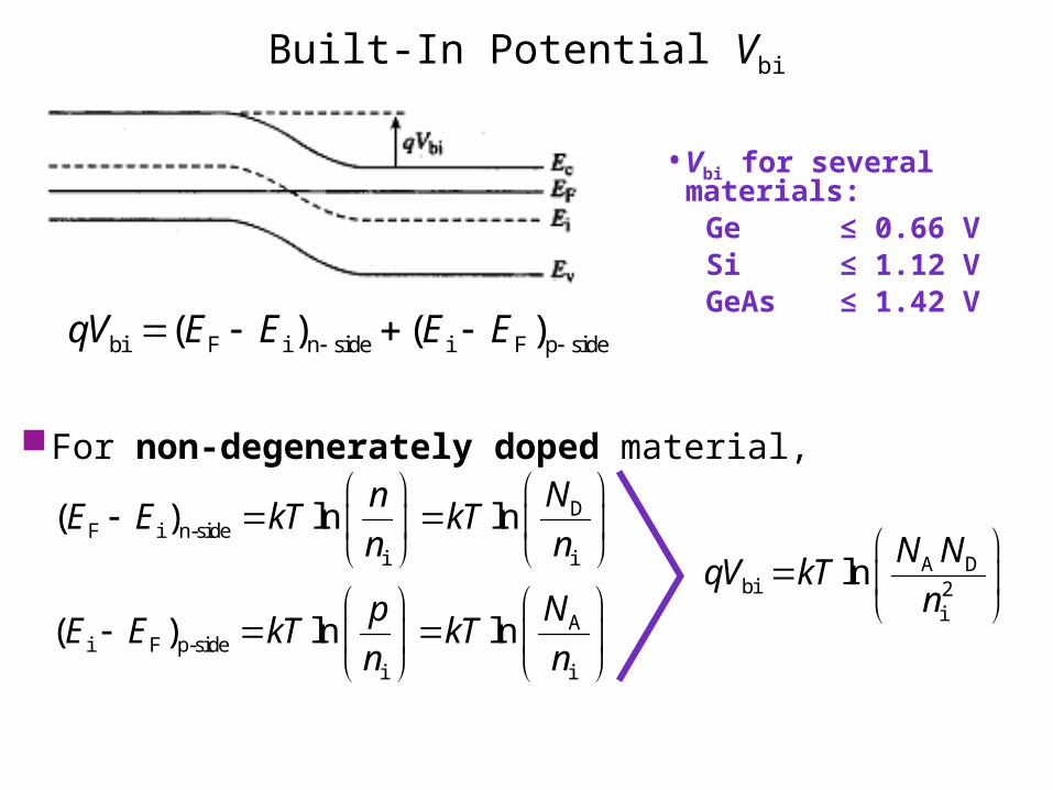
Step Junction with VA = 0
A p
D n
, 0 , 0 0,
qN x xqN x x
otherwise
Ap p
S
Dn n
S
( ), 0
( )( ), 0
qNx x x x
xqN
x x x x
E
2Ap p
S
2Dbi n n
S
( ) , 02
( )( ) , 0
2
qNx x x x
V xqN
V x x x x
Solution for ρ
Solution for E
Solution for V
Step Junction with VA = 0
2 2A Dp bi n
S S
( ) ( )2 2
qN qNx V x
A p D nN x N x
At x = 0, expressions for p-side and n-side for the solutions of E and V must be equal:

Relation between ρ(x), E(x), and V(x)
1.Find the profile of the built-in potential Vbi
2.Use the depletion approximation ρ(x) With depletion-layer widths xp, xn unknown
3.Integrate ρ(x) to find E(x) Boundary conditions E(–xp) 0, E(xn)0
4.Integrate E(x) to obtain V(x) Boundary conditions V(–xp) 0, V(xn) Vbi
5.For E(x) to be continuous at x 0, NAxp NDxn
Solve for xp, xn

Depletion Layer Width
S An bi
D A D
2
( )
Nx V
q N N N
S Dp bi
A A D
2
( )
Nx V
q N N N
n px x W
Dn
A
Nx
N
Eliminating xp,
Eliminating xn,
Summing Sbi
A D
2 1 1V
q N N
Exact solution, try to derive
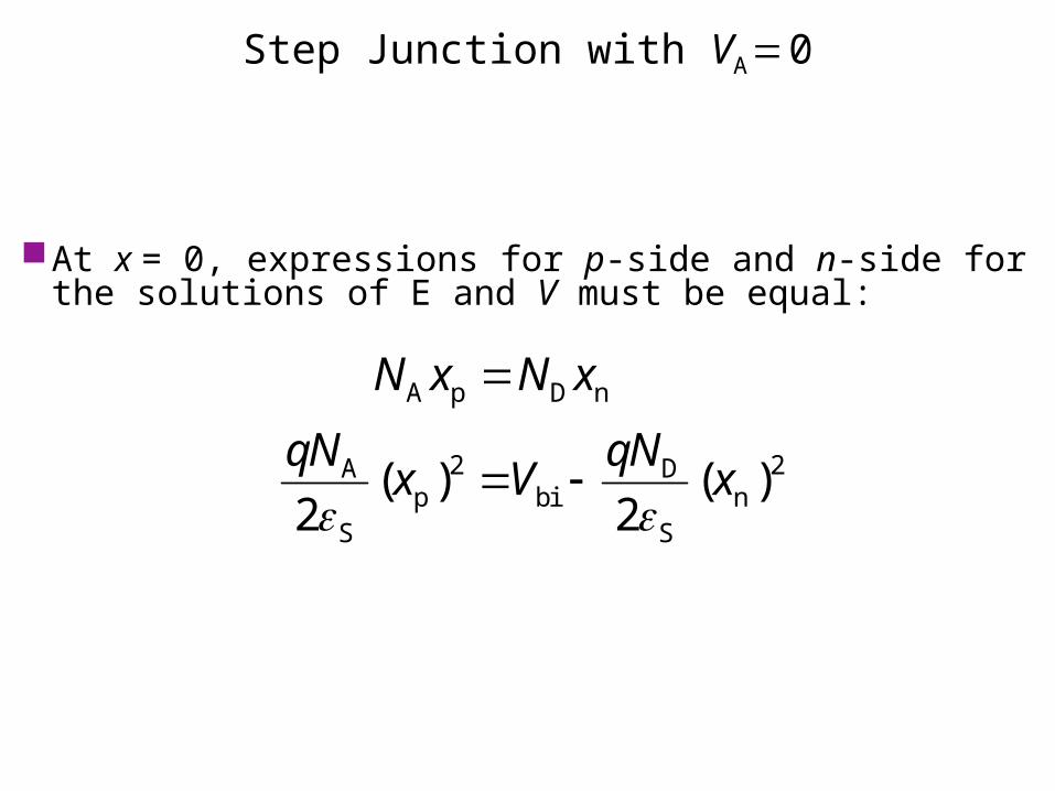
One-Sided Junctions
S bi Dn p n
D A
2 , 0
V NW x x x
q N N
S bi2 VW
q N
S bi Ap n p
A D
2 , 0
V NW x x x
q N N
If NA >> ND as in a p+n junction,
If ND >> NA as in a n+p junction,
Simplifying,
where N denotes the lighter dopant density
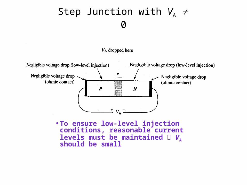
Step Junction with VA 0
• To ensure low-level injection conditions, reasonable current levels must be maintained VA should be small

Step Junction with VA 0
In the quasineutral, regions extending from the contacts to the edges of the depletion region, minority carrier diffusion equations can be applied since E ≈ 0.
In the depletion region, the continuity equations are applied.

Step Junction with VA 0
A Dbi
i i
ln lnN NkT kT
Vq n q n
Sp n bi A
A D
2 1 1W x x V V
q N N
S Dp bi A
A A D
2,
Nx V V
q N N N
S An bi A
D A D
2 Nx V V
q N N N
Built-in potential Vbi (non-degenerate doping):
A D2
i
lnN NkT
q n
Depletion width W :
,Dp
A D
Nx W
N N
W
NN
Nx
DA
An

Effect of Bias on Electrostatics
• If voltage drop â, then depletion width â• If voltage drop á, then depletion width á
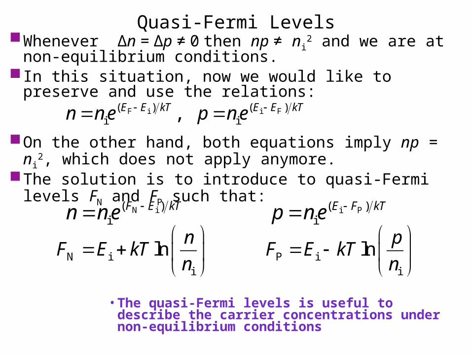
Quasi-Fermi Levels
F i i F( ) ( ) i i, E E kT E E kTn n e p n e
N i( )i
F E kTn n e i P( )i
E F kTp n e
P ii
lnp
F E kTn
N i
i
lnn
F E kTn
Whenever Δn = Δp ≠ 0 then np ≠ ni2 and we are at non-
equilibrium conditions. In this situation, now we would like to preserve and use the
relations:
On the other hand, both equations imply np = ni2, which does
not apply anymore.The solution is to introduce to quasi-Fermi levels FN and FP such that:
• The quasi-Fermi levels is useful to describe the carrier concentrations under non-equilibrium conditions

Example: Quasi-Fermi Levels
17 30 D 10 cm ,n N
23 3i
00
10 cmn
pn
17 14 17 30 10 +10 10 cmn n n
3 14 14 30 10 +10 10 cmp p p
17 14 31 310 10 =10 cmnp
a) What are p and n?
b) What is the np product?

Example: Quasi-Fermi LevelsConsider a Si sample at 300 K with ND = 1017 cm–3 and
Δn = Δp = 1014 cm–3.
c) Find FN and FP?
N i ilnF E kT n n
5 17 10N i 8.62 10 300 ln 10 10F E
0.417 eV
P i ilnF E kT p n
5 14 10i P 8.62 10 300 ln 10 10E F
0.238 eV
N i i P
i iF E kT E F kTnp n e n e
0.417 0.23810 100.02586 0.0258610 10e e
311.000257 10 31 310 cm
Ec
Ev
Ei
FP
0.238 eV
FN
0.417 eV
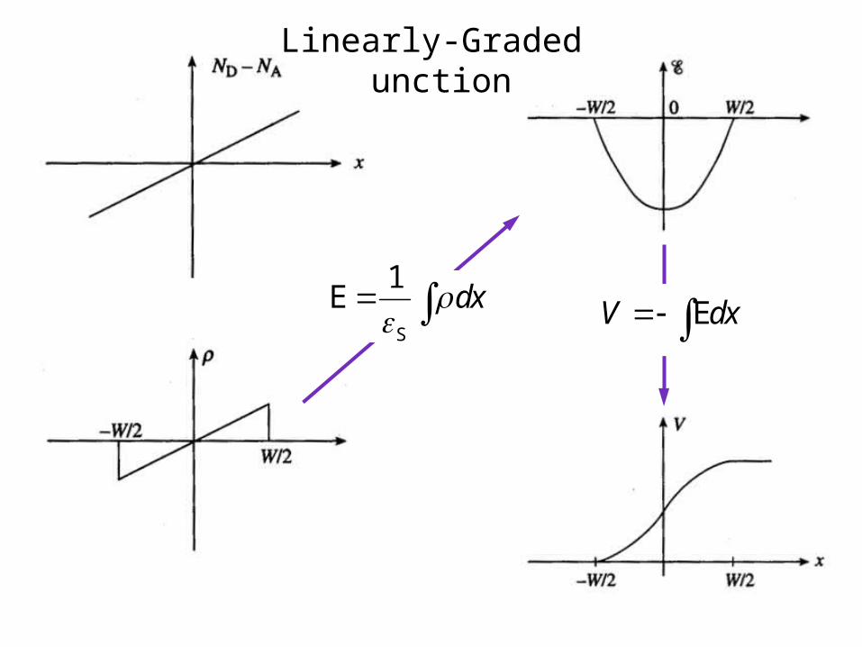
Linearly-Graded Junction
S
1dx
E V dx E

Linearly-Graded Junction Homework Assignment
Derive the relations of electrostatic variables, charge density and builtin voltage Vbi for the linearly graded junction.