Section 23. Serial Peripheral Interface (SPI) - KAZUS.RUkazus.ru/nuke/objects/lenta/6947/file/PIC24F...
26
© 2006 Microchip Technology Inc. Advance Information DS39699A-page 23-1 Serial Peripheral Interface (SPI) 23 Section 23. Serial Peripheral Interface (SPI) HIGHLIGHTS This section of the manual contains the following major topics: 23.1 Introduction .................................................................................................................. 23-2 23.2 Status and Control Registers ....................................................................................... 23-3 23.3 Modes of Operation ..................................................................................................... 23-7 23.4 Master Mode Clock Frequency .................................................................................. 23-18 23.5 Operation in Power-Saving Modes ............................................................................ 23-19 23.6 Register Maps ............................................................................................................ 23-20 23.7 Electrical Specifications ............................................................................................. 23-21 23.8 Related Application Notes.......................................................................................... 23-25 23.9 Revision History ......................................................................................................... 23-26
Transcript of Section 23. Serial Peripheral Interface (SPI) - KAZUS.RUkazus.ru/nuke/objects/lenta/6947/file/PIC24F...

Section 23. Serial Peripheral Interface (SPI)
Serial P
eriph
eralIn
terface (SP
I)
23
HIGHLIGHTSThis section of the manual contains the following major topics:23.1 Introduction .................................................................................................................. 23-223.2 Status and Control Registers ....................................................................................... 23-323.3 Modes of Operation ..................................................................................................... 23-7
23.4 Master Mode Clock Frequency .................................................................................. 23-1823.5 Operation in Power-Saving Modes ............................................................................ 23-1923.6 Register Maps............................................................................................................ 23-20
23.7 Electrical Specifications ............................................................................................. 23-2123.8 Related Application Notes.......................................................................................... 23-2523.9 Revision History ......................................................................................................... 23-26
© 2006 Microchip Technology Inc. Advance Information DS39699A-page 23-1
PIC24F Family Reference Manual
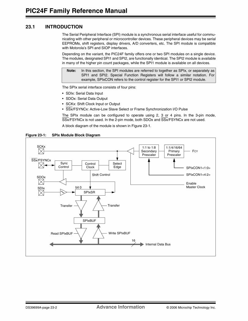
23.1 INTRODUCTION
The Serial Peripheral Interface (SPI) module is a synchronous serial interface useful for commu-nicating with other peripheral or microcontroller devices. These peripheral devices may be serialEEPROMs, shift registers, display drivers, A/D converters, etc. The SPI module is compatiblewith Motorola’s SPI and SIOP interfaces.
Depending on the variant, the PIC24F family offers one or two SPI modules on a single device.The modules, designated SPI1 and SPI2, are functionally identical. The SPI2 module is availablein many of the higher pin count packages, while the SPI1 module is available on all devices.
The SPIx serial interface consists of four pins:
• SDIx: Serial Data Input• SDOx: Serial Data Output
• SCKx: Shift Clock Input or Output• SSx/FSYNCx: Active-Low Slave Select or Frame Synchronization I/O Pulse
The SPIx module can be configured to operate using 2, 3 or 4 pins. In the 3-pin mode,SSx/FSYNCx is not used. In the 2-pin mode, both SDOx and SSx/FSYNCx are not used.
A block diagram of the module is shown in Figure 23-1.
Figure 23-1: SPIx Module Block Diagram
Note: In this section, the SPI modules are referred to together as SPIx, or separately asSPI1 and SPI2. Special Function Registers will follow a similar notation. Forexample, SPIxCON refers to the control register for the SPI1 or SPI2 module.
Internal Data Bus
SDIx
SDOx
SSx/FSYNCx
SCKx
SPIxSR
bit 0
Shift Control
EdgeSelect
FCYPrimary1:1/4/16/64
Enable
Prescaler
SyncClock
Control
SPIxBUF
Control
TransferTransfer
Write SPIxBUFRead SPIxBUF
16
SPIxCON1<1:0>
SPIxCON1<4:2>
Master Clock
SecondaryPrescaler
1:1 to 1:8
DS39699A-page 23-2 Advance Information © 2006 Microchip Technology Inc.
Section 23. Serial Peripheral Interface (SPI)S
erial Perip
heral
Interface (S
PI)
22
23.2 STATUS AND CONTROL REGISTERS
The SPI serial port consists of the following Special Function Registers:
• SPIxBUF: The address in SFR space that is used to buffer data to be transmitted and data that is received. This address is shared by the virtual SPIxTXB and SPIxRXB registers.
• SPIxCON1 and SPIxCON2: Control registers that configure the module for various modes of operation.
• SPIxSTAT: A status register that indicates various status conditions.
In addition, a 16-bit shift register, SPIxSR, is used for shifting data in and out of the SPI port. Theshift register is not memory mapped.
23.2.1 SPIxBUF Register
The memory mapped register, SPIxBUF, is the SPIx Data Receive/Transmit register. TheSPIxBUF register is actually comprised of two separate registers: the Transmit Buffer, SPIxTXB,and the Receive Buffer, SPIxRXB. These two unidirectional, 16-bit registers share the SFRaddress of SPIxBUF. If a user writes data to be transmitted to the SPIxBUF address, internallythe data is written to the SPIxTXB register. Similarly, when the user reads the received data fromSPIxBUF, internally the data is read from the SPIxRXB register.
This technique double-buffers transmit and receive operations and allows continuous datatransfers in the background. Transmission and reception occur simultaneously.
23.2.2 Status and Control Registers
The SPIxSTAT and SPIxCON1/SPIxCON2 registers provide the interface to control the module’soperation. They are shown in detail in Register 23-1, Register 23-2 and Register 23-3.
© 2006 Microchip Technology Inc. Advance Information DS39699A-page 23-3
PIC24F Family Reference Manual
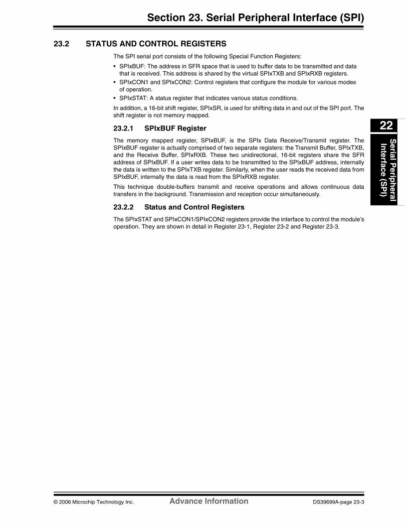
Register 23-1: SPIxSTAT: SPIx Status and Control Register
R/W-0 U-0 R/W-0 U-0 U-0 R-x R-x R-x
SPIEN — SPISIDL — — r r r
bit 15 bit 8
U-0 R/C-0 U-0 U-0 U-0 U-0 R-0 R-0
— SPIROV — — — — SPITBF SPIRBF
bit 7 bit 0
Legend: C = Clear only bit (cannot be set in software)
R = Readable bit W = Writable bit U = Unimplemented bit, read as ‘0’
-n = Value at POR ‘1’ = Bit is set ‘0’ = Bit is cleared x = Bit is unknown
bit 15 SPIEN: SPIx Enable bit
1 = Enables module and configures SCKx, SDOx, SDIx and SSx as serial port pins0 = Disables module
bit 14 Unimplemented: Read as ‘0’
bit 13 SPISIDL: Stop in Idle Mode bit1 = Discontinue module operation when device enters Idle mode0 = Continue module operation in Idle mode
bit 12-11 Unimplemented: Read as ‘0’
bit 10-8 Reserved: Value unknown
bit 7 Unimplemented: Read as ‘0’
bit 6 SPIROV: Receive Overflow Flag bit
1 = A new byte/word is completely received and discarded. The user software has not read the previous data in the SPIxBUF register.
0 = No overflow has occurred
bit 5-2 Unimplemented: Read as ‘0’
bit 1 SPITBF: SPIx Transmit Buffer Full Status bit1 = Transmit not yet started. SPIxTXB is full. Automatically set in hardware when CPU writes
SPIxBUF location, loading SPIxTXB.0 = Transmit started, SPIxTXB is empty. Automatically cleared in hardware when SPIx module
transfers data from SPIxTXB to SPIxSR.
bit 0 SPIRBF: SPIx Receive Buffer Full Status bit1 = Receive complete, SPIxRXB is full. Automatically set in hardware when SPIx transfers data
from SPIxSR to SPIxRXB.0 = Receive is not complete, SPIxRXB is empty. Automatically cleared in hardware when core reads
SPIxBUF location, reading SPIxRXB.
DS39699A-page 23-4 Advance Information © 2006 Microchip Technology Inc.

Section 23. Serial Peripheral Interface (SPI)S
erial Perip
heral
Interface (S
PI)
22
Register 23-2: SPIxCON1: SPIx Control Register 1
U-0 U-0 U-0 R/W-0 R/W-0 R/W-0 R/W-0 R/W-0
— — — DISSCK DISSDO MODE16 SMP CKE
bit 15 bit 8
R/W-0 R/W-0 R/W-0 R/W-0 R/W-0 R/W-0 R/W-0 R/W-0
SSEN CKP MSTEN SPRE2 SPRE1 SPRE0 PPRE1 PPRE0
bit 7 bit 0
Legend:
R = Readable bit W = Writable bit U = Unimplemented bit, read as ‘0’
-n = Value at POR ‘1’ = Bit is set ‘0’ = Bit is cleared x = Bit is unknown
bit 15-13 Unimplemented: Read as ‘0’
bit 12 DISSCK: Disable SCKx pin bit (SPIx Master modes only)
1 = Internal SPIx clock is disabled, pin functions as I/O0 = Internal SPIx clock is enabled
bit 11 DISSDO: Disable SDOx Pin bit1 = SDOx pin is not used by module, pin functions as I/O0 = SDOx pin is controlled by the module
bit 10 MODE16: Word/Byte Communication Select bit1 = Communication is word-wide (16 bits)0 = Communication is byte-wide (8 bits)
bit 9 SMP: SPIx Data Input Sample Phase bit
Master mode:1 = Input data sampled at end of data output time0 = Input data sampled at middle of data output timeSlave mode:SMP must be cleared when SPIx is used in Slave mode.
bit 8 CKE: SPIx Clock Edge Select bit1 = Serial output data changes on transition from active clock state to Idle clock state (see bit 6)0 = Serial output data changes on transition from Idle clock state to active clock state (see bit 6).
Note: The CKE bit is not used in the Framed SPIx modes. The user should program this bit to ‘0’for the Framed SPIx modes (FRMEN = 1).
bit 7 SSEN: Slave Select Enable (Slave mode) bit1 = SSx pin used for Slave mode0 = SSx pin not used by module, pin controlled by port function
bit 6 CKP: Clock Polarity Select bit1 = Idle state for clock is a high level; active state is a low level0 = Idle state for clock is a low level; active state is a high level
bit 5 MSTEN: Master Mode Enable bit
1 = Master mode0 = Slave mode
bit 4-2 SPRE2:SPRE0: Secondary Prescale bits (Master mode)111 = Secondary prescale 1:1110 = Secondary prescale 2:1...000 = Secondary prescale 8:1
bit 1-0 PPRE1:PPRE0: Primary Prescale bits (Master mode)11 = Primary prescale 1:110 = Primary prescale 4:101 = Primary prescale 16:100 = Primary prescale 64:1
© 2006 Microchip Technology Inc. Advance Information DS39699A-page 23-5
PIC24F Family Reference Manual
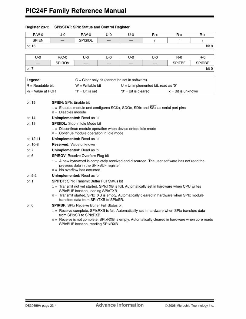
Register 23-3: SPIxCON2: SPIx Control Register 2
R/W-0 R/W-0 U-0 U-0 U-0 U-0 U-0 U-0
FRMEN SPIFSD SPIFPOL — — — — —
bit 15 bit 8
U-0 U-0 U-0 U-0 U-0 U-0 R/W-0 R-0
— — — — — — SPIFE r
bit 7 bit 0
Legend:
R = Readable bit W = Writable bit U = Unimplemented bit, read as ‘0’
-n = Value at POR ‘1’ = Bit is set ‘0’ = Bit is cleared x = Bit is unknown
bit 15 FRMEN: Framed SPIx Support bit1 = Framed SPIx support enabled0 = Framed SPIx support disabled
bit 14 SPIFSD: Frame Sync Pulse Direction Control on SSx pin bit
1 = Frame sync pulse input (slave)0 = Frame sync pulse output (master)
bit 13 SPIFPOL: Frame Sync Pulse Polarity Control on SSx pin bit (Framed modes only)1 = Frame sync pulse is active-high0 = Frame sync pulse is active-low
bit 12-2 Unimplemented: Read as ‘0’
bit 1 SPIFE: Frame Sync Pulse Edge Select bit
1 = Frame sync pulse coincides with first bit clock0 = Frame sync pulse precedes first bit clock
bit 0 Reserved: Maintain as ‘0’
DS39699A-page 23-6 Advance Information © 2006 Microchip Technology Inc.

Section 23. Serial Peripheral Interface (SPI)S
erial Perip
heral
Interface (S
PI)
22
23.3 MODES OF OPERATION
The SPI module has flexible operating modes which are discussed in the following subsections:
• 8-Bit and 16-Bit Data Transmission/Reception• Master and Slave Modes• Framed SPI Modes
23.3.1 8-Bit vs. 16-Bit Operation
The MODE16 control bit (SPIxCON1<10>) allows the module to communicate in either 8-bit or16-bit modes. The functionality will be the same for each mode, except for the number of bits thatare received and transmitted. Additionally, the following should be noted in this context:
The module is reset when the value of the MODE16 bit is changed. Consequently, the bit shouldnot be changed during normal operation.
Data is transmitted out of bit 7 of the SPIxSR for 8-bit operation, while it is transmitted out of bit 15of the SPIxSR for 16-bit operation. In both modes, data is shifted into bit 0 of the SPIxSR.
When transmitting or receiving data, 8 clock pulses at the SCKx pin are required to shift in/outdata in 8-bit mode, while 16 clock pulses are required in 16-bit mode.
23.3.2 Master and Slave Modes
Data can be thought of as taking a direct path between the Most Significant bit of one module’sshift register and the Least Significant bit of the other, and then into the appropriate Transmit orReceive Buffer. The module configured as the master module provides the serial clock and syn-chronization signals (as required) to the slave device. The relationship between the master andslave modules is shown in Figure 23-2.
Figure 23-2: SPIx Master/Slave Connection
Serial Receive Buffer(SPIxRXB)
Shift Register(SPIxSR)
LSbMSb
SDIx
SDOx
PROCESSOR 2 (SPIx Slave)
SCKx
SSx(1)
Serial Transmit Buffer(SPIxTXB)
Serial Receive Buffer(SPIxRXB)
Shift Register(SPIxSR)
MSb LSb
SDOx
SDIx
PROCESSOR 1 (SPIx Master)
Serial Clock
SSEN (SPIxCON1<7>) = 1 and MSTEN (SPIxCON1<5>) = 0
Note 1: Using the SSx pin in Slave mode of operation is optional.2: User must write transmit data to/read received data from SPIxBUF. The SPIxTXB and SPIxRXB registers are
memory mapped to SPIxBUF.
SSx
SCKx
Serial Transmit Buffer(SPIxTXB)
MSTEN (SPIxCON1<5>) = 1
SPIx Buffer(SPIxBUF)(2)
SPIx Buffer(SPIxBUF)(2)
© 2006 Microchip Technology Inc. Advance Information DS39699A-page 23-7

PIC24F Family Reference Manual
23.3.2.1 MASTER MODE
In Master mode, the system clock is prescaled and then used as the serial clock. The prescalingis based on the settings in the PPRE1:PPRE0 (SPIxCON1<1:0>) and SPRE2:SPRE0(SPIxCON1<4:2>) bits. The serial clock is output via the SCKx pin to slave devices. Clockpulses are only generated when there is data to be transmitted. For further information, refer toSection 23.4 “Master Mode Clock Frequency”. The CKP and CKE bits determine, on whichedge of the clock, data transmission occurs.
Both data to be transmitted and data that is received are respectively written into, or read from,the SPIxBUF register.
The following describes the SPIx module operation in Master mode:
1. Once the module is set up for Master mode of operation and enabled, data to betransmitted is written to the SPIxBUF register. The SPITBF (SPIxSTAT<1>) bit is set.
2. The contents of SPIxTXB are moved to the shift register, SPIxSR, and the SPITBF bit iscleared by the module.
3. A series of 8/16 clock pulses shifts out 8/16 bits of transmit data from the SPIxSR to theSDOx pin and simultaneously shifts in the data at the SDIx pin into the SPIxSR.
4. When the transfer is complete, the following events will occur:• The interrupt flag bit, SPIxIF, is set. SPIx interrupts can be enabled by setting the
interrupt enable bit, SPIxIE. The SPIxIF flag is not cleared automatically by the hardware.
• Also, when the ongoing transmit and receive operation is completed, the contents of the SPIxSR are moved to the SPIxRXB register.
• The SPIRBF (SPIxSTAT<0>) bit is set by the module, indicating that the receive buffer is full. Once the SPIxBUF register is read by the user code, the hardware clears the SPIRBF bit.
5. If the SPIRBF bit is set (receive buffer is full) when the SPIx module needs to transfer datafrom SPIxSR to SPIxRXB, the module will set the SPIROV (SPIxSTAT<6>) bit, indicatingan overflow condition.
6. Data to be transmitted can be written to SPIxBUF by the user software at any time as longas the SPITBF (SPIxSTAT<1>) bit is clear. The write can occur while SPIxSR is shiftingout the previously written data, allowing continuous transmission.
To set up the SPIx module for the Master mode of operation:
1. If using interrupts:• Clear the SPIxIF bit in the respective IFSn register.• Set the SPIxIE bit in the respective IECn register.
• Write the SPIxIP bits in the respective IPCn register to set the interrupt priority.2. Write the desired settings to the SPIxCON register with MSTEN (SPIxCON1<5>) = 1. 3. Clear the SPIROV bit (SPIxSTAT<6>).
4. Enable SPIx operation by setting the SPIEN bit (SPIxSTAT<15>).5. Write the data to be transmitted to the SPIxBUF register. Transmission (and reception) will
start as soon as data is written to the SPIxBUF register.
23.3.2.1.1 External Clocking in Master Mode
In Master mode, the module can also be configured to operate with an external data clock. SPIxclock operation is controlled by the DISSCK bit (SPIxCON1<12>). When this bit is set, the inter-nal data clock is disabled and data is transferred when external clock pulses are presented onthe SCKx pin. All other aspects of Master mode operation are the same as before.
Note: The SPIxSR register cannot be written into directly by the user. All writes to theSPIxSR register are performed through the SPIxBUF register.
Note: The DISSCK bit is available only in SPI Master modes.
DS39699A-page 23-8 Advance Information © 2006 Microchip Technology Inc.

Section 23. Serial Peripheral Interface (SPI)S
erial Perip
heral
Interface (S
PI)
22
Figure 23-3: SPIx Master Mode Timing
SCKx(CKP = 0
SCKx(CKP = 1
SCKx(CKP = 0
SCKx(CKP = 1
4 Clockmodes
InputSample
InputSample
SDIx
bit 7 bit 0
SDOxbit 7 bit 6 bit 5 bit 4 bit 3 bit 2 bit 1 bit 0
bit 7
SDIx
SPIxIF
(SMP = 1)(2)
(SMP = 0)(2)
(SMP = 1)(2)
CKE = 1)(1)
CKE = 0)(1)
CKE = 1)(1)
CKE = 0)(1)
(SMP = 0)(2)
User writesto SPIxBUF
SDOx bit 7 bit 6 bit 5 bit 4 bit 3 bit 2 bit 1 bit 0
(CKE = 0)
(CKE = 1)
1 instruction cycle latency to setSPIxIF flag bit
Note 1: Four SPIx Clock modes shown to demonstrate CKP (SPIxCON1<6>) and CKE (SPIxCON1<8>) bit functionality only.Only one of the four modes can be chosen for operation.
2: SDIx and input sample shown for two different values of the SMP (SPIxCON1<9>) bit, for demonstration purposesonly. Only one of the two configurations of the SMP bit can be chosen during operation.
3: If there are no pending transmissions, SPIxTXB is transferred to SPIxSR as soon as the user writes to SPIxBUF.4: Operation for 8-bit mode shown; the 16-bit mode is similar.
SPIxSR movedinto SPIxRXB
User readsSPIxBUF
(clock output at the SCKx
pin in Master mode)
(SPIxSTAT<0>)
SPITBF
SPIxTXB to SPIxSR(3) User writes new data
during transmission
SPIRBF
Two modesavailablefor SMPcontrolbit(4)
bit 0
© 2006 Microchip Technology Inc. Advance Information DS39699A-page 23-9

PIC24F Family Reference Manual
23.3.2.2 SLAVE MODE
In Slave mode, data is transmitted and received as the external clock pulses appear on the SCKxpin. The CKP (SPIxCON<6>) and CKE (SPIxCON<8>) bits determine on which edge of the clockdata transmission occurs. Both data to be transmitted and data that is received are respectivelywritten into or read from the SPIxBUF register. The rest of the operation of the module is identicalto that in the Master mode.
To set up the SPIx module for the Slave mode of operation:
1. Clear the SPIxBUF register.2. If using interrupts:
• Clear the SPIxIF bit in the respective IFSn register.
• Set the SPIxIE bit in the respective IECn register.• Write the SPIxIP bits in the respective IPCn register to set the interrupt priority.
3. Write the desired settings to the SPIxCON1 and SPIxCON2 registers with MSTEN(SPIxCON1<5>) = 0.
4. Clear the SMP bit.
5. If the CKE bit is set, then the SSEN bit (SPIxCON1<7>) must be set to enable the SSx pin.6. Clear the SPIROV bit (SPIxSTAT<6>).7. Enable SPIx operation by setting the SPIEN bit (SPIxSTAT<15>).
23.3.2.2.1 Slave Select Synchronization
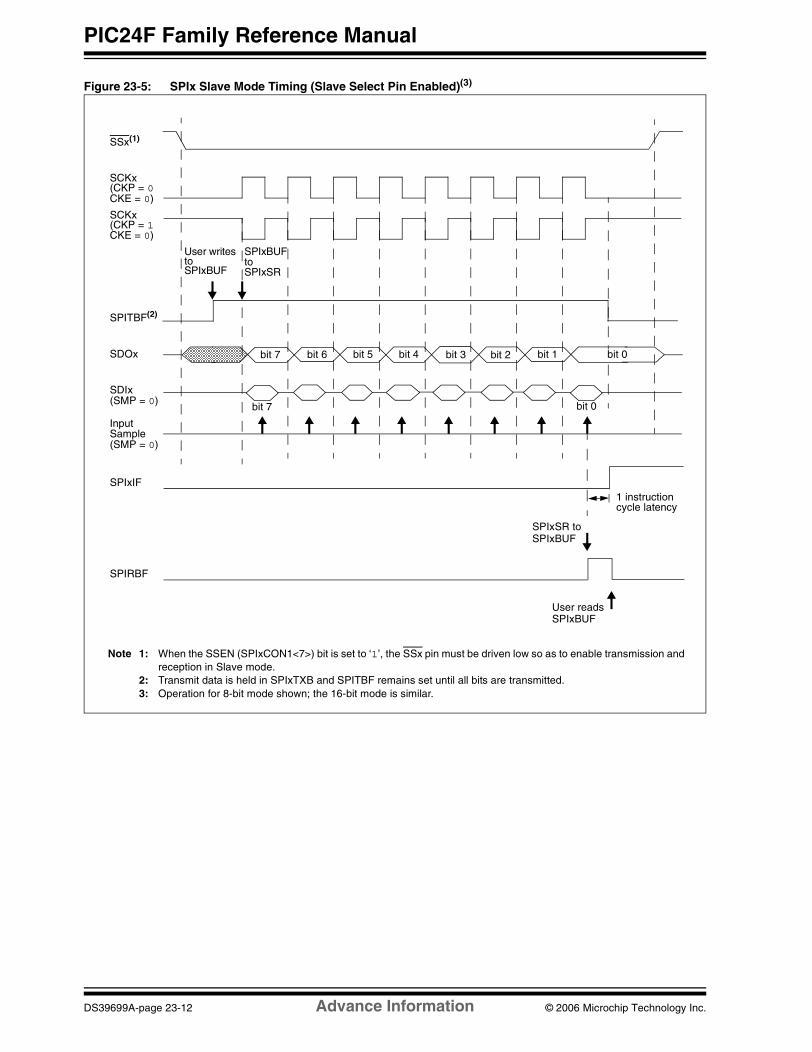
The SSx pin allows a Synchronous Slave mode. If the SSEN (SPIxCON1<7>) bit is set, trans-mission and reception are enabled in Slave mode only if the SSx pin is driven to a low state (seeFigure 23-5). The port output or other peripheral outputs must not be driven in order to allow theSSx pin to function as an input. If the SSEN bit is set and the SSx pin is driven high, the SDOxpin is no longer driven and will tri-state even if the module is in the middle of a transmission. Anaborted transmission will be retried the next time the SSx pin is driven low, using the data heldin the SPIxTXB register. If the SSEN bit is not set, the SSx pin does not affect the moduleoperation in Slave mode.
23.3.2.2.2 SPITBF Status Flag Operation
The function of the SPITBF (SPIxSTAT<1>) bit is different in the Slave mode of operation.
If SSEN (SPIxCON1<7>) is cleared, the SPITBF is set when the SPIxBUF is loaded by the usercode. It is cleared when the module transfers SPIxTXB to SPIxSR. This is similar to the SPITBFbit function in Master mode.
If SSEN is set, the SPITBF is set when the SPIxBUF is loaded by the user code. However, it iscleared only when the SPIx module completes data transmission. A transmission will be abortedwhen the SSx pin goes high and may be retried at a later time. Each data word is held in SPIxTXBuntil all bits are transmitted to the receiver.
Note: To meet module timing requirements, the SSx pin must be enabled in Slave modewhen CKE = 1 (refer to Figure 23-6 for details).
DS39699A-page 23-10 Advance Information © 2006 Microchip Technology Inc.
Section 23. Serial Peripheral Interface (SPI)S
erial Perip
heral
Interface (S
PI)
22
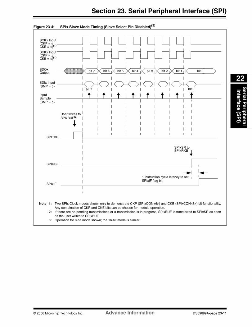
Figure 23-4: SPIx Slave Mode Timing (Slave Select Pin Disabled)(3)
SCKx Input(CKP = 1
SCKx Input(CKP = 0
InputSample
SDIx Input
bit 7 bit 0
SDOx bit 7 bit 6 bit 5 bit 4 bit 3 bit 2 bit 1 bit 0
SPIxIF
(SMP = 0)
CKE = 0)(1)
CKE = 0)(1)
(SMP = 0)
User writes toSPIxBUF(2)
SPIxSR toSPIxRXB
SPITBF
SPIRBF
Output
Note 1: Two SPIx Clock modes shown only to demonstrate CKP (SPIxCON<6>) and CKE (SPIxCON<8>) bit functionality.Any combination of CKP and CKE bits can be chosen for module operation.
2: If there are no pending transmissions or a transmission is in progress, SPIxBUF is transferred to SPIxSR as soonas the user writes to SPIxBUF.
3: Operation for 8-bit mode shown; the 16-bit mode is similar.
1 instruction cycle latency to setSPIxIF flag bit
© 2006 Microchip Technology Inc. Advance Information DS39699A-page 23-11
PIC24F Family Reference Manual
Figure 23-5: SPIx Slave Mode Timing (Slave Select Pin Enabled)(3)
SCKx(CKP = 1
SCKx(CKP = 0
InputSample
SDIx
bit 7 bit 0
SDOx bit 7 bit 6 bit 5 bit 4 bit 3 bit 2 bit 1
SPIxIF
(SMP = 0)
CKE = 0)
CKE = 0)
(SMP = 0)
User writes
SPIxBUF
SPIxSR toSPIxBUF
SSx(1)
Note 1: When the SSEN (SPIxCON1<7>) bit is set to ‘1’, the SSx pin must be driven low so as to enable transmission andreception in Slave mode.
2: Transmit data is held in SPIxTXB and SPITBF remains set until all bits are transmitted.3: Operation for 8-bit mode shown; the 16-bit mode is similar.
User readsSPIxBUF
SPIRBF
1 instructioncycle latency
SPITBF(2)
SPIxBUF to SPIxSR
to
bit 0
DS39699A-page 23-12 Advance Information © 2006 Microchip Technology Inc.

Section 23. Serial Peripheral Interface (SPI)S
erial Perip
heral
Interface (S
PI)
22
Figure 23-6: SPIx Slave Mode Timing (CKE = 1)(4)
SCK Input(CKP = 1
SCK Input(CKP = 0
InputSample
SDI Input
bit 7 bit 0
SDO bit 7 bit 6 bit 5 bit 4 bit 3 bit 2 bit 1 bit 0
SPIxIF
(SMP = 0)
CKE = 1)
CKE = 1)
(SMP = 0)
Write toSPIxBUF SPIxSR to
SPIxRXB
SSx(1,2)
SPITBF(3)
SPIRBF
Output
Note 1: The SSx pin must be used for Slave mode operation when CKE = 1.2: When the SSEN (SPIxCON1<7>) bit is set to ‘1’, the SSx pin must be driven low so as to enable transmission and
reception in Slave mode.3: Transmit data is held in SPIxTXB and SPITBF remains set until all bits are transmitted.4: Operation for 8-bit mode shown; the 16-bit mode is similar.
© 2006 Microchip Technology Inc. Advance Information DS39699A-page 23-13

PIC24F Family Reference Manual
23.3.3 Framed SPIx Modes
The module supports a basic framed SPIx protocol while operating in either Master or Slavemodes. The module uses four control bits to configure framed SPIx operation:
• FRMEN (SPIxCON2<15>) enables the Framed SPIx modes and causes the SSx pin to be used as a frame synchronization pulse input or output pin. The state of SSEN (SPIxCON1<7>) is ignored.
• SPIFSD (SPIxCON2<14>) determines whether the SSx pin is an input or an output (i.e., whether the module receives or generates the frame synchronization pulse).
• SPIFPOL (SPIxCON2<13>) selects the polarity of the frame synchronization pulse (active-high or active-low) for a single SPIx data frame.
• SPIFE (SPIxCON2<1>) selects the synchronization pulse to either coincide with, or precede, the first serial clock pulse.
The SPIx module supports two Framed modes of operation. In Framed Master mode, the SPIxmodule generates the frame synchronization pulse and provides this pulse to other devices atthe SSx/FSYNCx pin. In Framed Slave mode, the SPIx module uses a frame synchronizationpulse received at the SSx/FSYNCx pin.
The Framed SPIx modes are supported in conjunction with the unframed Master and Slavemodes. This makes four framed SPIx configurations available to the user:
• SPIx Master Mode and Framed Master Mode• SPIx Master Mode and Framed Slave Mode
• SPIx Slave Mode and Framed Master Mode• SPIx Slave Mode and Framed Slave Mode
These modes determine whether or not the SPIx module generates the serial clock and theframe synchronization pulse.
23.3.3.1 SCKx PIN IN FRAMED SPIx MODES
When FRMEN = 1 and MSTEN = 1, the SCKx pin becomes an output and the SPIx clock at SCKxbecomes a free-running clock. When FRMEN = 1 and MSTEN = 0, the SCKx pin becomes aninput. The source clock provided to the SCKx pin is assumed to be a free-running clock.
The polarity of the clock is selected by the CKP (SPIxCON1<6>) bit. The CKE (SPIxCON1<8>)bit is not used for the Framed SPIx modes and should be programmed to ‘0’ by the user software.When CKP = 0, the frame sync pulse output and the SDOx data output change on the rising edgeof the clock pulses at the SCKx pin. Input data is sampled at the SDIx input pin on the falling edgeof the serial clock. When CKP = 1, the frame sync pulse output and the SDOx data output changeon the falling edge of the clock pulses at the SCKx pin. Input data is sampled at the SDIx inputpin on the rising edge of the serial clock.
23.3.3.2 SPIx IN FRAMED SPIx MODES
When SPIFSD (SPIxCON2<13>) = 0, the SPIx module is in the Framed Master mode of opera-tion. In this mode, the frame sync pulse is initiated by the module when the user software writesthe transmit data to the SPIxBUF location (thus writing the SPIxTXB register with transmit data).At the end of the frame sync pulse, the SPIxTXB is transferred to the SPIxSR and datatransmission/reception begins.
When SPIFSD = 1, the module is in Framed Slave mode. In this mode, the frame sync pulse isgenerated by an external source. When the module samples the frame sync pulse, it will transferthe contents of the SPIxTXB register to the SPIxSR and data transmission/ reception begins. Theuser must make sure that the correct data is loaded into the SPIxBUF for transmission before theframe sync pulse is received.
Note: The use of the SSx/FSYNCx and SCKx pins are mandatory in all Framed SPIxmodes.
Note: Receiving a frame sync pulse will start a transmission, regardless of whether datawas written to SPIxBUF. If no write was performed, the old contents of the SPIxTXBwill be transmitted.
DS39699A-page 23-14 Advance Information © 2006 Microchip Technology Inc.

Section 23. Serial Peripheral Interface (SPI)S
erial Perip
heral
Interface (S
PI)
22
23.3.3.3 SPIx MASTER MODE AND FRAMED MASTER MODE
In Master/Framed Master mode, the SPIx module generates both the clock and frame synchro-nization signals, as shown in Figure 23-7. It is enabled by setting the MSTEN and FRMEN bitsto ‘1’ and the SPIFSD bit to ‘0’.
In this mode, the serial clock is output continuously at the SCKx pin, regardless of whether themodule is transmitting. When SPIxBUF is written, the FSYNCx pin will be driven to its active state(as determined by the SPIFPOL bit) on the appropriate transmit edge of the SCKx clock, andremain active for one data frame. If the SPIFE control bit (SPIxCON2<1>) is cleared, the framesync pulse precedes the data transmission, as shown in Figure 23-8. If SPIFE is set, the framesync pulse coincides with the beginning of the data transmission, as shown in Figure 23-9. Themodule starts transmitting data on the next transmit edge of the SCKx.
Figure 23-7: SPIx Master, Framed Master Connection Diagram
Figure 23-8: SPIx Master, Framed Master Timing (SPIFE = 0)
Figure 23-9: SPIx Master, Framed Master Timing (SPIFE = 1)
SDOx
SDIx
PIC24F
Serial Clock
SSx
SCKx
Frame SyncPulse
SDIx
SDOx
PROCESSOR 2
SSx
SCKx
(SPIx Slave, Framed Slave)
SCKx
FSYNCx
SDOx
(CKP = 0)
bit 14 bit 13 bit 12
SDIx
bit 14 bit 13 bit 12
Write to SPIxBUF Receive Samples at SDIx
Pulse Generated at SSx
SCKx(CKP = 1)
(SPIFPOL = 1)
FSYNCx(SPIFPOL = 0)
bit 15
bit 15
SCKx
SDOx
(CKP = 0)
bit 14 bit 13 bit 12
SDIx bit 14 bit 13 bit 12
Write to SPIxBUF Pulse Generated by FSYNCx,
SCKx(CKP = 1)
FSYNCx(SPIFPOL = 1)
FSYNCx(SPIFPOL = 0)
Receive Samples at SDIx
bit 15
bit 15
© 2006 Microchip Technology Inc. Advance Information DS39699A-page 23-15

PIC24F Family Reference Manual
23.3.3.4 SPIx MASTER MODE AND FRAMED SLAVE MODE
In Master/Framed Slave mode, the module generates the clock signal but uses the slavemodule’s frame synchronization signal for data transmission (Figure 23-10). It is enabled bysetting the MSTEN, FRMEN and SPIFSD bits to ‘1’.
In this mode, the FSYNCx pin is an input and it is sampled on the sample edge of the SPIx clock.When it is sampled in its active state, data will be transmitted on the subsequent transmit edgeof the SPIx clock. The interrupt flag, SPIxIF, is set when the transmission is complete. The usermust make sure that the correct data is loaded into the SPIxBUF for transmission before thesignal is received at the FSYNCx pin.
Figure 23-10: SPIx Master, Framed Slave Connection Diagram
Figure 23-11: SPIx Master, Framed Slave Timing (SPIFE = 0)
Figure 23-12: SPIx Master, Framed Slave Timing (SPIFE = 1)
SDOx
SDIx
PIC24F
Serial Clock
SSx
SCKx
Frame SyncPulse
SDIx
SDOx
PROCESSOR 2
SSx
SCKx
(SPIx Master, Framed Slave)
SCKx
SDOx
(CKP = 0)
bit 14 bit 13 bit 12
SDIx
Sample FSYNCx pin for Pulse
Receive Samples at SDIx
bit 14 bit 13 bit 12
Write to SPIxBUF
SCKx(CKP = 1)
FSYNCx(SPIFPOL = 1)
FSYNCx(SPIFPOL = 0)
bit 15
bit 15
SCKx
SDOx
(CKP = 0)
bit 14 bit 13 bit 12
SDIx bit 14 bit 13 bit 12
SCKx(CKP = 1)
Write to SPIxBUF Pulse Generated by FSYNCx,Receive Samples at SDIx
FSYNCx(SPIFPOL = 1)
FSYNCx(SPIFPOL = 0)
bit 15
bit 15
DS39699A-page 23-16 Advance Information © 2006 Microchip Technology Inc.

Section 23. Serial Peripheral Interface (SPI)S
erial Perip
heral
Interface (S
PI)
22
23.3.3.5 SPIx SLAVE MODE AND FRAMED MASTER MODE
In Slave/Framed Master mode, the module acts as the SPIx slave and takes its clock from theother SPIx module; however, it produces frame synchronization signals to control data transmis-sion (Figure 23-13). It is enabled by setting the MSTEN bit to ‘0’, the FRMEN bit to ‘1’ and theSPIFSD bit to ‘0’.
The input SPIx clock will be continuous in Slave mode. The FSYNCx pin will be an output whenthe SPIFSD bit is low. Therefore, when the SPIxBUF is written, the module drives the FSYNCxpin to the active state on the appropriate transmit edge of the SPIx clock for one SPIx clock cycle.Data will start transmitting on the appropriate SPIx clock transmit edge.
Figure 23-13: SPIx Slave, Framed Master Connection Diagram
23.3.3.6 SPIx SLAVE MODE AND FRAMED SLAVE MODE
In Slave/Framed Slave mode, the module obtains both its clock and frame synchronization signalfrom the master module (Figure 23-14). It is enabled by setting MSTEN to ‘0’, FRMEN to ‘1’ andSPIFSD to ‘1’.
In this mode, both the SCKx and FSYNCx pins will be inputs. The FSYNCx pin is sampled on thesample edge of the SPIx clock. When FSYNCx is sampled at its active state, data will betransmitted on the appropriate transmit edge of SCKx.
Figure 23-14: SPIx Slave, Framed Slave Connection Diagram
SDOx
SDIx
PIC24F
Serial Clock
SSx
SCKx
Frame SyncPulse
SDIx
SDOx
PROCESSOR 2
SSx
SCKx
(SPIx Slave, Framed Slave)
SDOx
SDIx
PIC24F
Serial Clock
SSx
SCKx
Frame SyncPulse
SDIx
SDOx
PROCESSOR 2
SSx
SCKx
(SPIx Master, Framed Slave)
© 2006 Microchip Technology Inc. Advance Information DS39699A-page 23-17

PIC24F Family Reference Manual
23.3.4 SPIx Receive Only Operation
Setting the DISSDO control bit (SPIxCON1<11>) disables transmission at the SDOx pin. Thisallows the SPIx module to be configured for a Receive Only mode of operation. The SDOx pinwill be controlled by the respective port function if the DISSDO bit is set.
The DISSDO function is applicable to all SPIx operating modes.
23.3.5 SPIx Error Handling
If a new data word has been shifted into SPIxSR and the previous SPIxBUF contents have notbeen read, the SPIROV bit (SPIxSTAT<6>) will be set. Any received data in SPIxSR will not betransferred and further data reception is disabled until the SPIROV bit is cleared. The SPIROVbit is not cleared automatically by the module; it must be cleared by the user software.
The SPIx Interrupt Flag, SPIxIF, is set whenever the SPIROV, SPIRBF (SPIxSTAT<0>) orSPITBF (SPIxSTAT<1>) bits are set. The interrupt flag cannot be cleared by hardware and mustbe reset in software. The actual SPIx interrupt is generated only when the corresponding SPIxIEbit is set in the IECn Control register
23.4 MASTER MODE CLOCK FREQUENCY
In the Master mode, the clock provided to the SPIx module is the instruction cycle (TCY). Thisclock will then be prescaled by the primary prescaler, specified by PPRE1:PPRE0(SPIxCON1<1:0>), and the secondary prescaler, specified by SPRE2:SPRE0(SPIxCON1<4:2>). The prescaled instruction clock becomes the serial clock and is provided toexternal devices via the SCKx pin.
Equation 23-1 can be used to calculate the SCKx clock frequency as a function of the primaryand secondary prescaler settings.
Equation 23-1:
Some sample SPIx clock frequencies (in kHz) are shown in Table 23-1 below:
Table 23-1: Sample SCKx Frequencies(1,2)
Note: Note that the SCKx signal clock is not free running for normal SPI modes. It will onlyrun for 8 or 16 pulses when the SPIxBUF is loaded with data. It will, however, becontinuous for Framed modes.
Primary Prescaler * Secondary Prescaler
FCY FSCK =
FCY = 16 MHzSecondary Prescaler Settings
1:1 2:1 4:1 6:1 8:1
Primary Prescaler Settings 1:1 16000 8000 4000 2667 2000
4:1 4000 2000 1000 667 500
16:1 1000 500 250 167 125
64:1 250 125 63 42 31
FCY = 5 MHz
Primary Prescaler Settings 1:1 5000 2500 1250 833 625
4:1 1250 625 313 208 156
16:1 313 156 78 52 39
64:1 78 39 20 13 10
Note 1: Based on TCY = TOSC/2, Doze mode and PLL are disabled.2:SCKx frequencies shown in kHz.
Note: Not all clock rates are supported. For further information, refer to the SPIx timingspecifications in the specific device data sheet.
DS39699A-page 23-18 Advance Information © 2006 Microchip Technology Inc.

Section 23. Serial Peripheral Interface (SPI)S
erial Perip
heral
Interface (S
PI)
22
23.5 OPERATION IN POWER-SAVING MODES
The PIC24F family of devices has three Power modes: the normal operational (Full-Power)mode, and the two Power-Saving modes invoked by the PWRSAV instruction. Depending on theSPIx mode selected, entering a Power-Saving mode may also affect the operation of the module.
23.5.1 Sleep Mode
When the device enters Sleep mode, the system clock is disabled. The consequences ofentering Sleep depend on which mode (Master or Slave) the module is configured in at the timethat Sleep mode is invoked.
23.5.1.1 MASTER MODE OPERATION
The following are a consequence of entering Sleep mode when the SPIx module is configuredfor master operation:
• The Baud Rate Generator in the SPIx module stops and is reset.
• The transmitter and receiver will stop in Sleep. The transmitter or receiver does not continue with a partially completed transmission at wake-up.
• If the SPIx module enters Sleep mode in the middle of a transmission or reception, the transmission or reception is aborted. Since there is no automatic way to prevent an entry into Sleep mode if a transmission or reception is pending, the user software must synchronize entry into Sleep with SPIx module operation to avoid aborted transmissions.
23.5.1.2 SLAVE MODE OPERATION
Since the clock pulses at SCKx are externally provided for Slave mode, the module will continueto function in Sleep mode. It will complete any transactions during the transition into Sleep. Oncompletion of a transaction, the SPIRBF flag is set. Consequently, the SPIxIF bit will be set. IfSPIx interrupts are enabled (SPIxIE = 1), the device will wake from Sleep. If the SPIx interruptpriority level is greater than the present CPU priority level, code execution will resume at the SPIxinterrupt vector location. Otherwise, code execution will continue with the instruction following thePWRSAV instruction that previously invoked Sleep mode. The module is not reset on enteringSleep mode if it is operating as a slave device.
Register contents are not affected when the SPIx module is going into or coming out of Sleepmode.
23.5.2 Idle Mode
When the device enters Idle mode, the system clock sources remain functional. The SPISIDL bit(SPIxSTAT<13>) selects whether the module will stop or continue functioning on Idle.
If SPISIDL = 1, the SPIx module will stop communication on entering Idle mode. It will operatein the same manner as it does in Sleep mode. If SPISID = 0 (default selection), the module willcontinue operation in Idle mode.
© 2006 Microchip Technology Inc. Advance Information DS39699A-page 23-19

PIC24F Family Reference Manual
23.6
RE
GIS
TE
R M
AP
SA
sum
mar
y of
the
regi
ster
s as
soci
ated
with
the
PIC
24F
SP
I mod
ule
is p
rovi
ded
in T
able
23-2
.
Tab
le 2
3-2:
SP
I Mem
ory
Map
Nam
eB
it 1
5B
it 1
4B
it 1
3B
it 1
2B
it 1
1B
it 1
0B
it 9
Bit
8B
it 7
Bit
6B
it 5
Bit
4B
it 3
Bit
2B
it 1
Bit
0A
ll R
eset
s
SP
IxS
TAT
SP
IEN
—S
PIS
IDL
——
rr
r—
SP
IRO
V—
——
—S
PIT
BF
SP
IRB
F0000
SP
IxC
ON
1—
——
DIS
SC
KD
ISS
DO
MO
DE
16S
MP
CK
ES
SE
NC
KP
MS
TE
NS
PR
E2
SP
RE
1S
PR
E1
PP
RE
1P
PR
E0
0000
SP
IxC
ON
2F
RM
EN
SP
IFS
DS
PIF
PO
L—
——
——
——
——
——
SP
IFE
r0000
SP
IxB
UF
SP
Ix T
rans
mit
and
Rec
eive
Buf
fer
0000
PM
D1
T5M
DT
4MD
T3M
DT
2MD
T1M
D—
——
I2C
1MD
U2M
DU
1MD
SP
I2M
DS
PI1
MD
——
AD
CM
D0000
PM
D2
——
—IC
5MD
IC4M
DIC
3MD
IC2M
DIC
1MD
——
—O
C5M
DO
C4M
DO
C3M
DO
C2M
DO
C1M
D0000
PM
D3
——
——
—C
MP
MD
RT
CC
MD
PM
PM
DC
RC
PM
D—
——
——
I2C
MD
—0000
Leg
end
:—
= u
nim
plem
ente
d, r
ead
as '0
’. R
eset
val
ues
are
show
n in
hex
idec
imal
.
DS39699A-page 23-20 © 2006 Microchip Technology Inc.

Section 23. Serial Peripheral Interface (SPI)S
erial Perip
heral
Interface (S
PI)
22
23.7 ELECTRICAL SPECIFICATIONS
Figure 23-15: SPIx Module Master Mode Timing Characteristics (CKE = 0)
Table 23-3: SPIx Master Mode Timing Requirements (CKE = 0)
AC CHARACTERISTICSStandard Operating Conditions: 2.0V to 3.6V(unless otherwise stated)Operating temperature -40°C ≤ TA ≤ +85°C for Industrial
ParamNo.
Symbol Characteristic Min Typ(1) Max Units Conditions
SP10 TscL SCKx Output Low Time(2) TCY/2 — — ns
SP11 TscH SCKx Output High Time(2) TCY/2 — — ns
SP20 TscF SCKx Output Fall Time(3) — 10 25 ns
SP21 TscR SCKx Output Rise Time(3) — 10 25 ns
SP30 TdoF SDOx Data Output Fall Time(3) — 10 25 ns
SP31 TdoR SDOx Data Output Rise Time(3) — 10 25 ns
SP35 TscH2doV,TscL2doV
SDOx Data Output Valid after SCKx Edge
— — 30 ns
SP40 TdiV2scH,TdiV2scL
Setup Time of SDIx Data Inputto SCKx Edge
20 — — ns
SP41 TscH2diL,TscL2diL
Hold Time of SDIx Data Inputto SCKx Edge
20 — — ns
Note 1: Data in “Typ” column is at 3.3V, 25°C unless otherwise stated. Parameters are for design guidance only and are not tested.
2: The minimum clock period for SCKx is 100 ns. Therefore, the clock generated in Master mode must not violate this specification.
3: Assumes 50 pF load on all SPI pins.
SCKx(CKP = 0)
SCKx(CKP = 1)
SDOx
SDIx
SP11 SP10
SP40 SP41
SP21SP20SP35
SP20SP21
MSb LSbBit 14 - - - - - -1
LSb InBit 14 - - - -1
SP30SP31
MSb In
© 2006 Microchip Technology Inc. Advance Information DS39699A-page 23-21

PIC24F Family Reference Manual
Figure 23-16: SPIx Module Master Mode Timing Characteristics (CKE = 1)
Table 23-4: SPIx Module Master Mode Timing Requirements (CKE = 1)
AC CHARACTERISTICSStandard Operating Conditions: 2.0V to 3.6V(unless otherwise stated)Operating temperature -40°C ≤ TA ≤ +85°C for Industrial
ParamNo.
Symbol Characteristic Min Typ(1) Max Units Conditions
SP10 TscL SCKx Output Low Time(2) TCY/2 — — ns
SP11 TscH SCKx Output High Time(2) TCY/2 — — ns
SP20 TscF SCKx Output Fall Time(3) — 10 25 ns
SP21 TscR SCKx Output Rise Time(3) — 10 25 ns
SP30 TdoF SDOx Data Output Fall Time(3) — 10 25 ns
SP31 TdoR SDOx Data Output Rise Time(3) — 10 25 ns
SP35 TscH2doV,TscL2doV
SDOx Data Output Valid afterSCKx Edge
— — 30 ns
SP36 TdoV2sc, TdoV2scL
SDOx Data Output Setup toFirst SCKx Edge
30 — — ns
SP40 TdiV2scH, TdiV2scL
Setup Time of SDIx Data Inputto SCKx Edge
20 — — ns
SP41 TscH2diL, TscL2diL
Hold Time of SDIx Data Inputto SCKx Edge
20 — — ns
Note 1: Data in “Typ” column is at 3.3V, 25°C unless otherwise stated. Parameters are for design guidance only and are not tested.
2: The minimum clock period for SCKx is 100 ns. Therefore, the clock generated in Master mode must not violate this specification.
3: Assumes 50 pF load on all SPI pins.
SCKx(CKP = 0)
SCKx(CKP = 1)
SDOx
SDIx
SP36
SP30,SP31
SP35
MSb Bit 14 - - - - - -1
LSb InBit 14 - - - -1
LSb
SP11 SP10
SP21SP20
SP41
MSb In
SP40
SP20SP21
DS39699A-page 23-22 Advance Information © 2006 Microchip Technology Inc.

Section 23. Serial Peripheral Interface (SPI)S
erial Perip
heral
Interface (S
PI)
22
Figure 23-17: SPIx Module Slave Mode Timing Characteristics (CKE = 0)
Table 23-5: SPIx Module Slave Mode Timing Requirements (CKE = 0)
AC CHARACTERISTICSStandard Operating Conditions: 2.0V to 3.6V(unless otherwise stated)Operating temperature -40°C ≤ TA ≤ +85°C for Industrial
ParamNo.
Symbol Characteristic Min Typ(1) Max Units Conditions
SP70 TscL SCKx Input Low Time 30 — — ns
SP71 TscH SCKx Input High Time 30 — — ns
SP72 TscF SCKx Input Fall Time(2) — 10 25 ns
SP73 TscR SCKx Input Rise Time(2) — 10 25 ns
SP30 TdoF SDOx Data Output Fall Time(2) — 10 25 ns
SP31 TdoR SDOx Data Output Rise Time(2) — 10 25 ns
SP35 TscH2doV,TscL2doV
SDOx Data Output Valid afterSCKx Edge
— — 30 ns
SP40 TdiV2scH, TdiV2scL
Setup Time of SDIx Data Inputto SCKx Edge
20 — — ns
SP41 TscH2diL, TscL2diL
Hold Time of SDIx Data Inputto SCKx Edge
20 — — ns
SP50 TssL2scH, TssL2scL
SSx to SCKx↑ or SCKx Input 120 — — ns
SP51 TssH2doZ SSx↑ to SDOx OutputHigh-Impedance(3)
10 — 50 ns
SP52 TscH2ssHTscL2ssH
SSx after SCKx Edge 1.5 TCY + 40 — — ns
Note 1: Data in “Typ” column is at 3.3V, 25°C unless otherwise stated. Parameters are for design guidance only and are not tested.
2: Assumes 50 pF load on all SPI pins.
SSx
SCKx(CKP = 0)
SCKx(CKP = 1)
SDOx
SDI
SP50
SP40
SP41
SP30,SP31 SP51
SP35
SDIx
MSb LSbBit 14 - - - - - -1
Bit 14 - - - -1 LSb In
SP52
SP73SP72
SP72SP73SP71 SP70
MSb In
© 2006 Microchip Technology Inc. Advance Information DS39699A-page 23-23

PIC24F Family Reference Manual
Figure 23-18: SPIx Module Slave Mode Timing Characteristics (CKE = 1)
SSx
SCKx(CKP = 0)
SCKx(CKP = 1)
SDOx
SP60
SDIx
SP30,SP31
MSb Bit 14 - - - - - -1 LSb
SP51
Bit 14 - - - -1 LSb In
SP35
SP52
SP52
SP73SP72
SP72SP73SP71 SP70
SP40
SP41
SP50
MSb In
Table 23-6: SPIx Module Slave Mode Timing Requirements (CKE = 1)
AC CHARACTERISTICSStandard Operating Conditions: 2.0V to 3.6V(unless otherwise stated)Operating temperature -40°C ≤ TA ≤ +85°C for Industrial
ParamNo.
Symbol Characteristic Min Typ(1) Max Units Conditions
SP70 TscL SCKx Input Low Time 30 — — ns
SP71 TscH SCKx Input High Time 30 — — ns
SP72 TscF SCKx Input Fall Time(2) — 10 25 ns
SP73 TscR SCKx Input Rise Time(2) — 10 25 ns
SP30 TdoF SDOx Data Output Fall Time(2) — 10 25 ns
SP31 TdoR SDOx Data Output Rise Time(2) — 10 25 ns
SP35 TscH2doV,TscL2doV
SDOx Data Output Valid after SCKx Edge — — 30 ns
SP40 TdiV2scH, TdiV2scL
Setup Time of SDIx Data Input to SCKx Edge
20 — — ns
SP41 TscH2diL, TscL2diL
Hold Time of SDIx Data Input to SCKx Edge
20 — — ns
SP50 TssL2scH, TssL2scL
SSx↓ to SCKx↓ or SCKx↑ Input 120 — — ns
SP51 TssH2doZ SSx↑ to SDOx Output High-Impedance(3) 10 — 50 ns
SP52 TscH2ssHTscL2ssH
SSx↑ after SCKx Edge 1.5 TCY + 40 — — ns
SP60 TssL2doV SDOx Data Output Valid after SSx Edge — — 50 ns
Note 1: Data in “Typ” column is at 3.3V, 25°C unless otherwise stated. Parameters are for design guidance only and are not tested.
2: The minimum clock period for SCKx is 100 ns. Therefore, the clock generated in Master mode must not violate this specification.
3: Assumes 50 pF load on all SPI pins.
DS39699A-page 23-24 Advance Information © 2006 Microchip Technology Inc.
Section 23. Serial Peripheral Interface (SPI)S
erial Perip
heral
Interface (S
PI)
22
23.8 RELATED APPLICATION NOTES
This section lists application notes that are related to this section of the manual. Theseapplication notes may not be written specifically for the PIC24F device family, but the conceptsare pertinent and could be used with modification and possible limitations. The currentapplication notes related to the Serial Peripheral Interface (SPI) module are:
Title Application Note #
Interfacing Microchip’s MCP41XXX and MCP42XXX Digital Potentiometers to a PICmicro® Microcontroller AN746
Interfacing Microchip’s MCP3201 Analog-to-Digital Converter to the PICmicro® Microcontroller AN719
Note: Please visit the Microchip web site (www.microchip.com) for additional applicationnotes and code examples for the PIC24F family of devices.
© 2006 Microchip Technology Inc. Advance Information DS39699A-page 23-25

PIC24F Family Reference Manual
23.9 REVISION HISTORY
Revision A (August 2006)
This is the initial released revision of this document.
DS39699A-page 23-26 Advance Information © 2006 Microchip Technology Inc.