
SCLS107F –DECEMBER 1982–REVISED … · Charged-device model (CDM), per JEDEC specification...
30
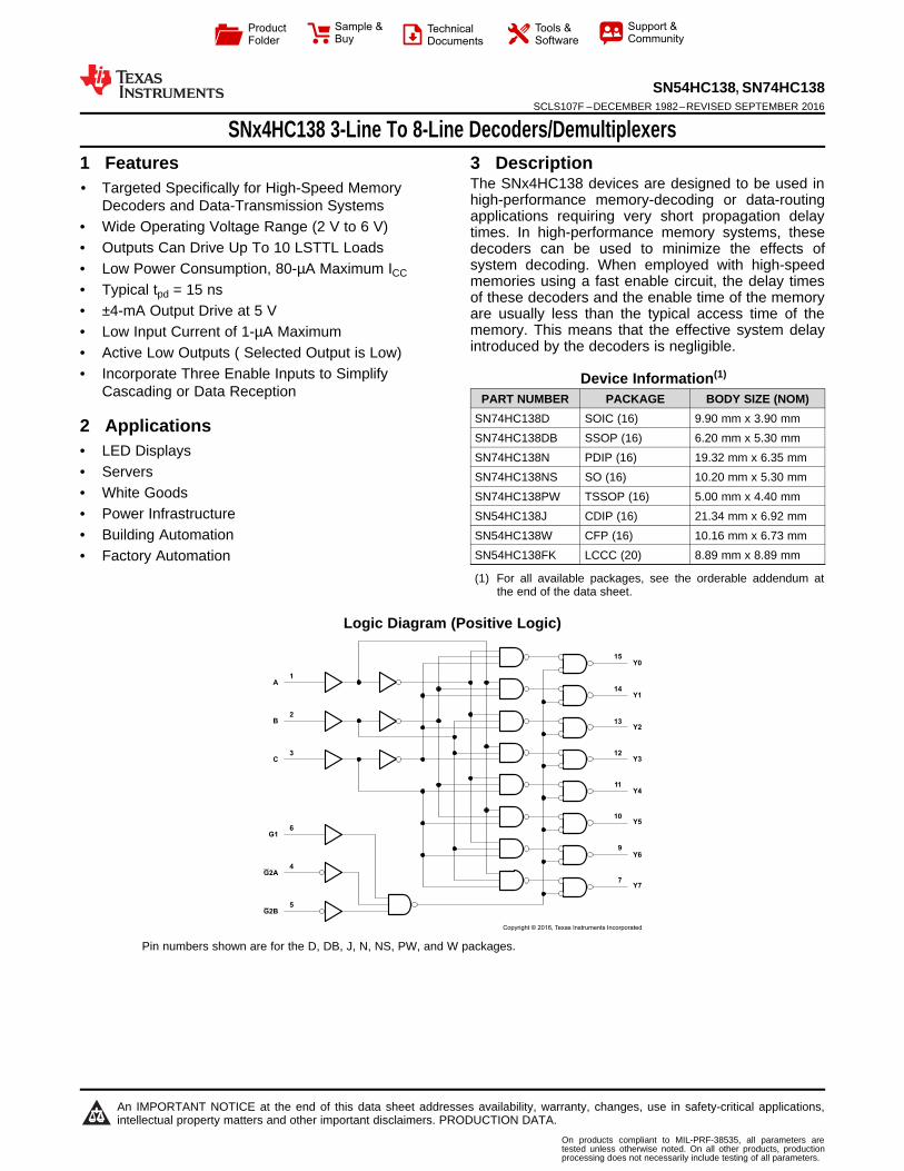
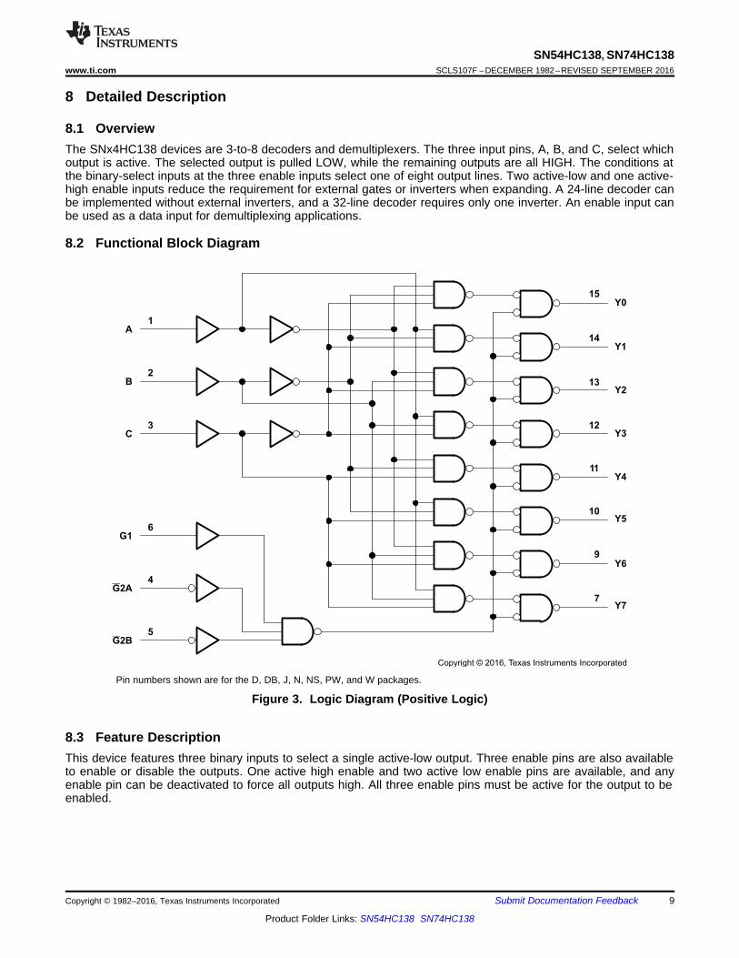
A Y0 Y1 Y2 Y3 Y4 Y5 Y6 Y7 B C G1 G 2A G 2B 1 2 3 6 4 5 15 14 13 12 11 10 9 7 Copyright © 2016, Texas Instruments Incorporated Product Folder Sample & Buy Technical Documents Tools & Software Support & Community An IMPORTANT NOTICE at the end of this data sheet addresses availability, warranty, changes, use in safety-critical applications, intellectual property matters and other important disclaimers. PRODUCTION DATA. On products compliant to MIL-PRF-38535, all parameters are tested unless otherwise noted. On all other products, production processing does not necessarily include testing of all parameters. SN54HC138, SN74HC138 SCLS107F – DECEMBER 1982 – REVISED SEPTEMBER 2016 SNx4HC138 3-Line To 8-Line Decoders/Demultiplexers 1 1 Features 1• Targeted Specifically for High-Speed Memory Decoders and Data-Transmission Systems • Wide Operating Voltage Range (2 V to 6 V) • Outputs Can Drive Up To 10 LSTTL Loads • Low Power Consumption, 80-μA Maximum I CC • Typical t pd = 15 ns • ±4-mA Output Drive at 5 V • Low Input Current of 1-μA Maximum • Active Low Outputs ( Selected Output is Low) • Incorporate Three Enable Inputs to Simplify Cascading or Data Reception 2 Applications • LED Displays • Servers • White Goods • Power Infrastructure • Building Automation • Factory Automation 3 Description The SNx4HC138 devices are designed to be used in high-performance memory-decoding or data-routing applications requiring very short propagation delay times. In high-performance memory systems, these decoders can be used to minimize the effects of system decoding. When employed with high-speed memories using a fast enable circuit, the delay times of these decoders and the enable time of the memory are usually less than the typical access time of the memory. This means that the effective system delay introduced by the decoders is negligible. Device Information (1) PART NUMBER PACKAGE BODY SIZE (NOM) SN74HC138D SOIC (16) 9.90 mm x 3.90 mm SN74HC138DB SSOP (16) 6.20 mm x 5.30 mm SN74HC138N PDIP (16) 19.32 mm x 6.35 mm SN74HC138NS SO (16) 10.20 mm x 5.30 mm SN74HC138PW TSSOP (16) 5.00 mm x 4.40 mm SN54HC138J CDIP (16) 21.34 mm x 6.92 mm SN54HC138W CFP (16) 10.16 mm x 6.73 mm SN54HC138FK LCCC (20) 8.89 mm x 8.89 mm (1) For all available packages, see the orderable addendum at the end of the data sheet. Logic Diagram (Positive Logic) Pin numbers shown are for the D, DB, J, N, NS, PW, and W packages.
Transcript of SCLS107F –DECEMBER 1982–REVISED … · Charged-device model (CDM), per JEDEC specification...
A
Y0
Y1
Y2
Y3
Y4
Y5
Y6
Y7
B
C
G1
G2A
G2B
1
2
3
6
4
5
15
14
13
12
11
10
9
7
Copyright © 2016, Texas Instruments Incorporated
Product
Folder
Sample &Buy
Technical
Documents
Tools &
Software
Support &Community
An IMPORTANT NOTICE at the end of this data sheet addresses availability, warranty, changes, use in safety-critical applications,intellectual property matters and other important disclaimers. PRODUCTION DATA.
On products compliant to MIL-PRF-38535, all parameters aretested unless otherwise noted. On all other products, productionprocessing does not necessarily include testing of all parameters.
SN54HC138, SN74HC138SCLS107F –DECEMBER 1982–REVISED SEPTEMBER 2016
SNx4HC138 3-Line To 8-Line Decoders/Demultiplexers
1
1 Features1• Targeted Specifically for High-Speed Memory
Decoders and Data-Transmission Systems• Wide Operating Voltage Range (2 V to 6 V)• Outputs Can Drive Up To 10 LSTTL Loads• Low Power Consumption, 80-µA Maximum ICC
• Typical tpd = 15 ns• ±4-mA Output Drive at 5 V• Low Input Current of 1-µA Maximum• Active Low Outputs ( Selected Output is Low)• Incorporate Three Enable Inputs to Simplify
Cascading or Data Reception
2 Applications• LED Displays• Servers• White Goods• Power Infrastructure• Building Automation• Factory Automation
3 DescriptionThe SNx4HC138 devices are designed to be used inhigh-performance memory-decoding or data-routingapplications requiring very short propagation delaytimes. In high-performance memory systems, thesedecoders can be used to minimize the effects ofsystem decoding. When employed with high-speedmemories using a fast enable circuit, the delay timesof these decoders and the enable time of the memoryare usually less than the typical access time of thememory. This means that the effective system delayintroduced by the decoders is negligible.
Device Information(1)
PART NUMBER PACKAGE BODY SIZE (NOM)SN74HC138D SOIC (16) 9.90 mm x 3.90 mmSN74HC138DB SSOP (16) 6.20 mm x 5.30 mmSN74HC138N PDIP (16) 19.32 mm x 6.35 mmSN74HC138NS SO (16) 10.20 mm x 5.30 mmSN74HC138PW TSSOP (16) 5.00 mm x 4.40 mmSN54HC138J CDIP (16) 21.34 mm x 6.92 mmSN54HC138W CFP (16) 10.16 mm x 6.73 mmSN54HC138FK LCCC (20) 8.89 mm x 8.89 mm
(1) For all available packages, see the orderable addendum atthe end of the data sheet.
Logic Diagram (Positive Logic)
Pin numbers shown are for the D, DB, J, N, NS, PW, and W packages.
2
SN54HC138, SN74HC138SCLS107F –DECEMBER 1982–REVISED SEPTEMBER 2016 www.ti.com
Product Folder Links: SN54HC138 SN74HC138
Submit Documentation Feedback Copyright © 1982–2016, Texas Instruments Incorporated
Table of Contents1 Features .................................................................. 12 Applications ........................................................... 13 Description ............................................................. 14 Revision History..................................................... 25 Pin Configuration and Functions ......................... 36 Specifications......................................................... 4
6.1 Absolute Maximum Ratings ...................................... 46.2 ESD Ratings: SN74HC138 ....................................... 46.3 Recommended Operating Conditions....................... 46.4 Thermal Information: SN74HC138............................ 56.5 Thermal Information: SN54HC138............................ 56.6 Electrical Characteristics........................................... 56.7 Electrical Characteristics: SN74HC138 .................... 66.8 Electrical Characteristics: SN54HC138 .................... 66.9 Switching Characteristics .......................................... 66.10 Switching Characteristics: SN74HC138.................. 76.11 Switching Characteristics: SN54HC138.................. 76.12 Typical Characteristic.............................................. 7
7 Parameter Measurement Information .................. 88 Detailed Description .............................................. 9
8.1 Overview ................................................................... 98.2 Functional Block Diagram ......................................... 98.3 Feature Description................................................... 98.4 Device Functional Modes........................................ 10
9 Application and Implementation ........................ 119.1 Application Information............................................ 119.2 Typical Application .................................................. 11
10 Power Supply Recommendations ..................... 1211 Layout................................................................... 12
11.1 Layout Guidelines ................................................. 1211.2 Layout Example .................................................... 12
12 Device and Documentation Support ................. 1312.1 Documentation Support ........................................ 1312.2 Related Links ........................................................ 1312.3 Receiving Notification of Documentation Updates 1312.4 Community Resources.......................................... 1312.5 Trademarks ........................................................... 1312.6 Electrostatic Discharge Caution............................ 1312.7 Glossary ................................................................ 13
13 Mechanical, Packaging, and OrderableInformation ........................................................... 13
4 Revision HistoryNOTE: Page numbers for previous revisions may differ from page numbers in the current version.
Changes from Revision E (September 2003) to Revision F Page
• Added ESD Ratings table, Feature Description section, Device Functional Modes, Application and Implementationsection, Power Supply Recommendations section, Layout section, Device and Documentation Support section, andMechanical, Packaging, and Orderable Information section .................................................................................................. 1
• Deleted Ordering Information table; see POA at the end of the data sheet........................................................................... 1• Changed RθJA values from 73 to 87.3 (D), from 82 to 104.3 (DB), from 67 to 54.8 (N), from 64 to 91.1 (NS), and
from 108 to 114.6 (PW) .......................................................................................................................................................... 5
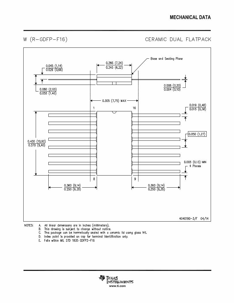
4C
5G2A
6NC
7G2B
8G1
9Y
7
10G
ND
11N
C
12Y
6
13Y
5
14 Y4
15 Y3
16 NC
17 Y2
18 Y1
19Y
0
20V
CC
1N
C
2A
3B
Not to scale
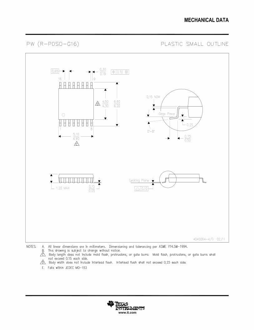
1A 16 VCC
2B 15 Y0
3C 14 Y1
4G2A 13 Y2
5G2B 12 Y3
6G1 11 Y4
7Y7 10 Y5
8GND 9 Y6
Not to scale
3
SN54HC138, SN74HC138www.ti.com SCLS107F –DECEMBER 1982–REVISED SEPTEMBER 2016
Product Folder Links: SN54HC138 SN74HC138
Submit Documentation FeedbackCopyright © 1982–2016, Texas Instruments Incorporated
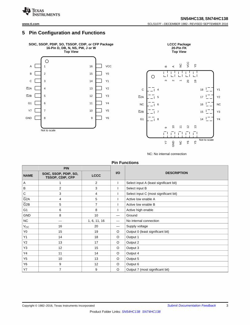
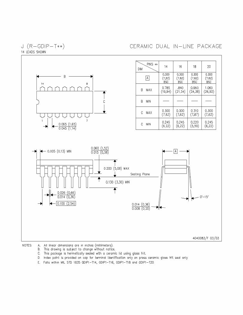
5 Pin Configuration and Functions
SOIC, SSOP, PDIP, SO, TSSOP, CDIP, or CFP Package16-Pin D, DB, N, NS, PW, J or W
Top View
LCCC Package20-Pin FKTop View
NC: No internal connection
Pin FunctionsPIN
I/O DESCRIPTIONNAME SOIC, SSOP, PDIP, SO,
TSSOP, CDIP, CFP LCCC
A 1 2 I Select input A (least significant bit)B 2 3 I Select input BC 3 4 I Select input C (most significant bit)G2A 4 5 I Active low enable AG2B 5 7 I Active low enable BG1 6 8 I Active high enableGND 8 10 — GroundNC — 1, 6, 11, 16 — No internal connectionVCC 16 20 — Supply voltageY0 15 19 O Output 0 (least significant bit)Y1 14 18 O Output 1Y2 13 17 O Output 2Y3 12 15 O Output 3Y4 11 14 O Output 4Y5 10 13 O Output 5Y6 9 12 O Output 6Y7 7 9 O Output 7 (most significant bit)
4
SN54HC138, SN74HC138SCLS107F –DECEMBER 1982–REVISED SEPTEMBER 2016 www.ti.com
Product Folder Links: SN54HC138 SN74HC138
Submit Documentation Feedback Copyright © 1982–2016, Texas Instruments Incorporated
(1) Stresses beyond those listed under Absolute Maximum Ratings may cause permanent damage to the device. These are stress ratingsonly, which do not imply functional operation of the device at these or any other conditions beyond those indicated under RecommendedOperating Conditions. Exposure to absolute-maximum-rated conditions for extended periods may affect device reliability.
(2) The input and output voltage ratings may be exceeded if the input and output current ratings are observed.
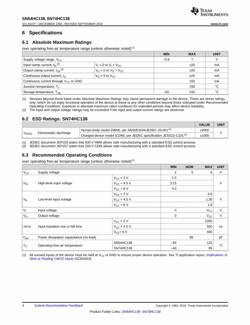
6 Specifications
6.1 Absolute Maximum Ratingsover operating free-air temperature range (unless otherwise noted) (1)
MIN MAX UNITSupply voltage range, VCC –0.5 7 VInput clamp current, IIK(2) VI < 0 or VI > VCC ±20 mAOutput clamp current, IOK
(2) VO < 0 or VO > VCC ±20 mAContinuous output current, IO VO = 0 to VCC ±25 mAContinuous current through VCC or GND ±50 mAJunction temperature, TJ 150 °CStorage temperature, Tstg –65 150 °C
(1) JEDEC document JEP155 states that 500-V HBM allows safe manufacturing with a standard ESD control process.(2) JEDEC document JEP157 states that 250-V CDM allows safe manufacturing with a standard ESD control process.
6.2 ESD Ratings: SN74HC138VALUE UNIT
V(ESD) Electrostatic dischargeHuman-body model (HBM), per ANSI/ESDA/JEDEC JS-001 (1) ±2000
VCharged-device model (CDM), per JEDEC specification JESD22-C101 (2) ±1000
(1) All unused inputs of the device must be held at VCC or GND to ensure proper device operation. See TI application report, Implications ofSlow or Floating CMOS Inputs (SCBA004).
6.3 Recommended Operating Conditionsover operating free-air temperature range (unless otherwise noted) (1)
MIN NOM MAX UNITVCC Supply voltage 2 5 6 V
VIH High-level input voltageVCC = 2 V 1.5
VVCC = 4.5 V 3.15VCC = 6 V 4.2
VIL Low-level input voltageVCC = 2 V 0.5
VVCC = 4.5 V 1.35VCC = 6 V 1.8
VI Input voltage 0 VCC VVO Output voltage 0 VCC V
Δt/Δv Input transition rise or fall timeVCC = 2 V 1000
nsVCC = 4.5 V 500VCC= 6 V 400
Cpd Power dissipation capacitance (no load) 85 pF
TA Operating free-air temperatureSN54HC138 –55 125
°CSN74HC138 –40 85
5
SN54HC138, SN74HC138www.ti.com SCLS107F –DECEMBER 1982–REVISED SEPTEMBER 2016
Product Folder Links: SN54HC138 SN74HC138
Submit Documentation FeedbackCopyright © 1982–2016, Texas Instruments Incorporated
(1) For more information about traditional and new thermal metrics, see the Semiconductor and IC Package Thermal Metrics applicationreport.
6.4 Thermal Information: SN74HC138
THERMAL METRIC (1)SN74HC138
UNITD (SOIC) DB (SSOP) N (PDIP) NS (SO) PW (TSSOP)16 PINS 16 PINS 16 PINS 16 PINS 16 PINS
RθJA Junction-to-ambient thermal resistance 87.3 104.3 54.8 91.1 114.6 °C/WRθJC(top) Junction-to-case (top) thermal resistance 45.8 54.7 42.1 49.5 49.5 °C/WRθJB Junction-to-board thermal resistance 44.8 54.9 34.8 51.5 59.6 °C/W
ψJTJunction-to-top characterizationparameter 14.2 17.7 27 17.8 6.9 °C/W
ψJBJunction-to-board characterizationparameter 44.5 54.4 34.7 51.2 59.1 °C/W
(1) For more information about traditional and new thermal metrics, see the Semiconductor and IC Package Thermal Metrics applicationreport.
(2) RθJC follows MIL-STD-883, and RθJB follows JESD51.
6.5 Thermal Information: SN54HC138
THERMAL METRIC (1)SN54HC138 (2)
UNITJ (CDIP) W (CFP) FK (LCCC)16 PINS 16 PINS 20 PINS
RθJA Junction-to-ambient thermal resistance — — — °C/WRθJC(top) Junction-to-case (top) thermal resistance 45.4 68.1 49 °C/WRθJB Junction-to-board thermal resistance — 118.4 47.7 °C/WψJT Junction-to-top characterization parameter — — 7.2 °C/WψJB Junction-to-board characterization parameter 62.5 — — °C/WRθJC(bot) Junction-to-case (bottom) thermal resistance 17.7 9 — °C/W
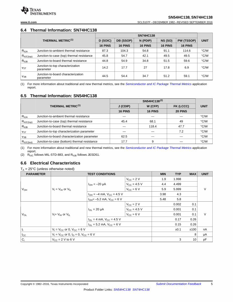
6.6 Electrical CharacteristicsTA = 25°C (unless otherwise noted)
PARAMETER TEST CONDITIONS MIN TYP MAX UNIT
VOH VI = VIH or VIL
IOH = –20 µAVCC = 2 V 1.9 1.998
VVCC = 4.5 V 4.4 4.499VCC = 6 V 5.9 5.999
IOH = –4 mA, VCC = 4.5 V 3.98 4.3IOH= –5.2 mA, VCC = 6 V 5.48 5.8
VOL VI= VIH or VIL
IOL = 20 µAVCC = 2 V 0.002 0.1
VVCC = 4.5 V 0.001 0.1VCC = 6 V 0.001 0.1
IOL = 4 mA, VCC = 4.5 V 0.17 0.26IOL = 5.2 mA, VCC = 6 V 0.15 0.26
II VI = VCC or 0, VCC = 6 V ±0.1 ±100 nAICC VI = VCC or 0, IO = 0, VCC = 6 V 8 µACi VCC = 2 V to 6 V 3 10 pF
6
SN54HC138, SN74HC138SCLS107F –DECEMBER 1982–REVISED SEPTEMBER 2016 www.ti.com
Product Folder Links: SN54HC138 SN74HC138
Submit Documentation Feedback Copyright © 1982–2016, Texas Instruments Incorporated
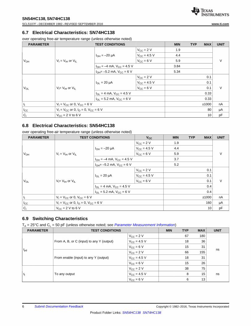
6.7 Electrical Characteristics: SN74HC138over operating free-air temperature range (unless otherwise noted)
PARAMETER TEST CONDITIONS MIN TYP MAX UNIT
VOH VI = VIH or VIL
IOH = –20 µAVCC = 2 V 1.9
VVCC = 4.5 V 4.4VCC = 6 V 5.9
IOH = –4 mA, VCC = 4.5 V 3.84IOH= –5.2 mA, VCC = 6 V 5.34
VOL VI= VIH or VIL
IOL = 20 µAVCC = 2 V 0.1
VVCC = 4.5 V 0.1VCC = 6 V 0.1
IOL = 4 mA, VCC = 4.5 V 0.33IOL = 5.2 mA, VCC = 6 V 0.33
II VI = VCC or 0, VCC = 6 V ±1000 nAICC VI = VCC or 0, IO = 0, VCC = 6 V 80 µACi VCC = 2 V to 6 V 10 pF
6.8 Electrical Characteristics: SN54HC138over operating free-air temperature range (unless otherwise noted)
PARAMETER TEST CONDITIONS VCC MIN TYP MAX UNIT
VOH VI = VIH or VIL
IOH = –20 µAVCC = 2 V 1.9
VVCC = 4.5 V 4.4VCC = 6 V 5.9
IOH = –4 mA, VCC = 4.5 V 3.7IOH= –5.2 mA, VCC = 6 V 5.2
VOL VI= VIH or VIL
IOL = 20 µAVCC = 2 V 0.1
VVCC = 4.5 V 0.1VCC = 6 V 0.1
IOL = 4 mA, VCC = 4.5 V 0.4IOL = 5.2 mA, VCC = 6 V 0.4
II VI = VCC or 0, VCC = 6 V ±1000 nAICC VI = VCC or 0, IO = 0, VCC = 6 V 160 µACi VCC = 2 V to 6 V 10 pF
6.9 Switching CharacteristicsTA = 25°C and CL = 50 pF (unless otherwise noted; see Parameter Measurement Information)
PARAMETER TEST CONDITIONS MIN TYP MAX UNIT
tpd
From A, B, or C (input) to any Y (output)VCC = 2 V 67 180
ns
VCC = 4.5 V 18 36VCC = 6 V 15 31
From enable (input) to any Y (output)VCC = 2 V 66 155VCC = 4.5 V 18 31VCC = 6 V 15 26
tt To any outputVCC = 2 V 38 75
nsVCC = 4.5 V 8 15VCC = 6 V 6 13
Supply Voltage VCC (V)
Pro
paga
tion
Del
ay F
rom
A, B
, C to
any
Y (
ns)
2 2.5 3 3.5 4 4.5 5 5.5 615
20
25
30
35
40
45
50
55
60
65
70
D001
7
SN54HC138, SN74HC138www.ti.com SCLS107F –DECEMBER 1982–REVISED SEPTEMBER 2016
Product Folder Links: SN54HC138 SN74HC138
Submit Documentation FeedbackCopyright © 1982–2016, Texas Instruments Incorporated
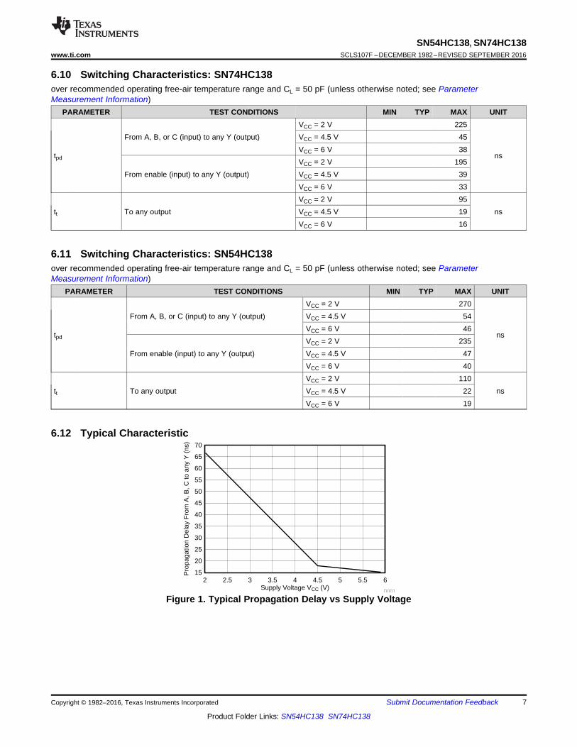
6.10 Switching Characteristics: SN74HC138over recommended operating free-air temperature range and CL = 50 pF (unless otherwise noted; see ParameterMeasurement Information)
PARAMETER TEST CONDITIONS MIN TYP MAX UNIT
tpd
From A, B, or C (input) to any Y (output)VCC = 2 V 225
ns
VCC = 4.5 V 45VCC = 6 V 38
From enable (input) to any Y (output)VCC = 2 V 195VCC = 4.5 V 39VCC = 6 V 33
tt To any outputVCC = 2 V 95
nsVCC = 4.5 V 19VCC = 6 V 16
6.11 Switching Characteristics: SN54HC138over recommended operating free-air temperature range and CL = 50 pF (unless otherwise noted; see ParameterMeasurement Information)
PARAMETER TEST CONDITIONS MIN TYP MAX UNIT
tpd
From A, B, or C (input) to any Y (output)VCC = 2 V 270
ns
VCC = 4.5 V 54VCC = 6 V 46
From enable (input) to any Y (output)VCC = 2 V 235VCC = 4.5 V 47VCC = 6 V 40
tt To any outputVCC = 2 V 110
nsVCC = 4.5 V 22VCC = 6 V 19
6.12 Typical Characteristic
Figure 1. Typical Propagation Delay vs Supply Voltage
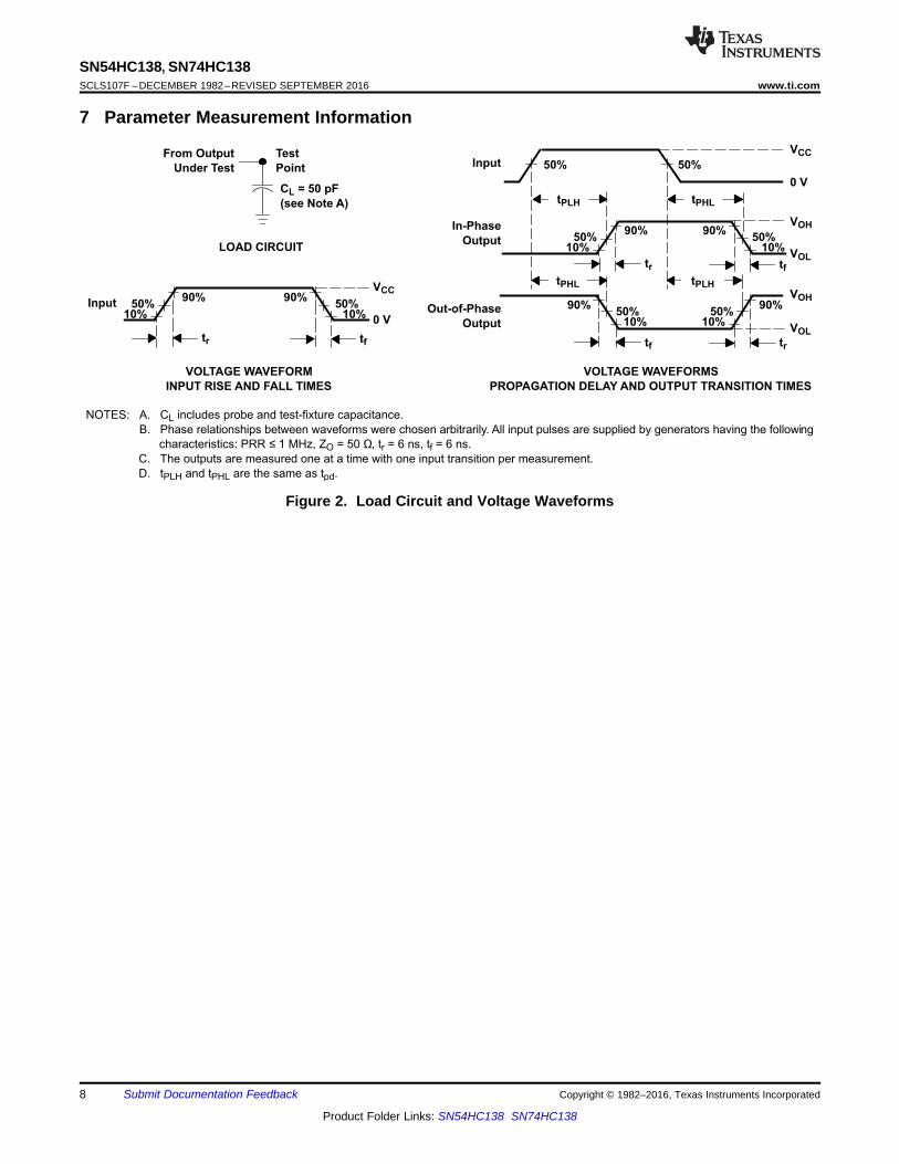
VOLTAGE WAVEFORM
INPUT RISE AND FALL TIMES
50%50%10%10%
90% 90%VCC
0 V
tr t
Input
f
VOLTAGE WAVEFORMS
PROPAGATION DELAY AND OUTPUT TRANSITION TIMES
50%
50%50%10%10%
90% 90%
VCC
VOH
VOL
0 V
tr t
Input
f
In-Phase
Output
50%
tPLH tPHL
50% 50%10% 10%
90%90%VOH
VOL
tt rf
tPHL tPLH
Out-of-Phase
Output
Test
Point
From Output
Under Test
CL = 50 pF
(see Note A)
LOAD CIRCUIT
NOTES: A. CL includes probe and test-fixture capacitance.
B. Phase relationships between waveforms were chosen arbitrarily. All input pulses are supplied by generators having the following
characteristics: PRR ≤ 1 MHz, ZO = 50 Ω, tr = 6 ns, tf = 6 ns.
C. The outputs are measured one at a time with one input transition per measurement.
D. tPLH and tPHL are the same as tpd.
8
SN54HC138, SN74HC138SCLS107F –DECEMBER 1982–REVISED SEPTEMBER 2016 www.ti.com
Product Folder Links: SN54HC138 SN74HC138
Submit Documentation Feedback Copyright © 1982–2016, Texas Instruments Incorporated
7 Parameter Measurement Information
Figure 2. Load Circuit and Voltage Waveforms
A
Y0
Y1
Y2
Y3
Y4
Y5
Y6
Y7
B
C
G1
G2A
G2B
1
2
3
6
4
5
15
14
13
12
11
10
9
7
Copyright © 2016, Texas Instruments Incorporated
9
SN54HC138, SN74HC138www.ti.com SCLS107F –DECEMBER 1982–REVISED SEPTEMBER 2016
Product Folder Links: SN54HC138 SN74HC138
Submit Documentation FeedbackCopyright © 1982–2016, Texas Instruments Incorporated
8 Detailed Description
8.1 OverviewThe SNx4HC138 devices are 3-to-8 decoders and demultiplexers. The three input pins, A, B, and C, select whichoutput is active. The selected output is pulled LOW, while the remaining outputs are all HIGH. The conditions atthe binary-select inputs at the three enable inputs select one of eight output lines. Two active-low and one active-high enable inputs reduce the requirement for external gates or inverters when expanding. A 24-line decoder canbe implemented without external inverters, and a 32-line decoder requires only one inverter. An enable input canbe used as a data input for demultiplexing applications.
8.2 Functional Block Diagram
Pin numbers shown are for the D, DB, J, N, NS, PW, and W packages.
Figure 3. Logic Diagram (Positive Logic)
8.3 Feature DescriptionThis device features three binary inputs to select a single active-low output. Three enable pins are also availableto enable or disable the outputs. One active high enable and two active low enable pins are available, and anyenable pin can be deactivated to force all outputs high. All three enable pins must be active for the output to beenabled.
10
SN54HC138, SN74HC138SCLS107F –DECEMBER 1982–REVISED SEPTEMBER 2016 www.ti.com
Product Folder Links: SN54HC138 SN74HC138
Submit Documentation Feedback Copyright © 1982–2016, Texas Instruments Incorporated
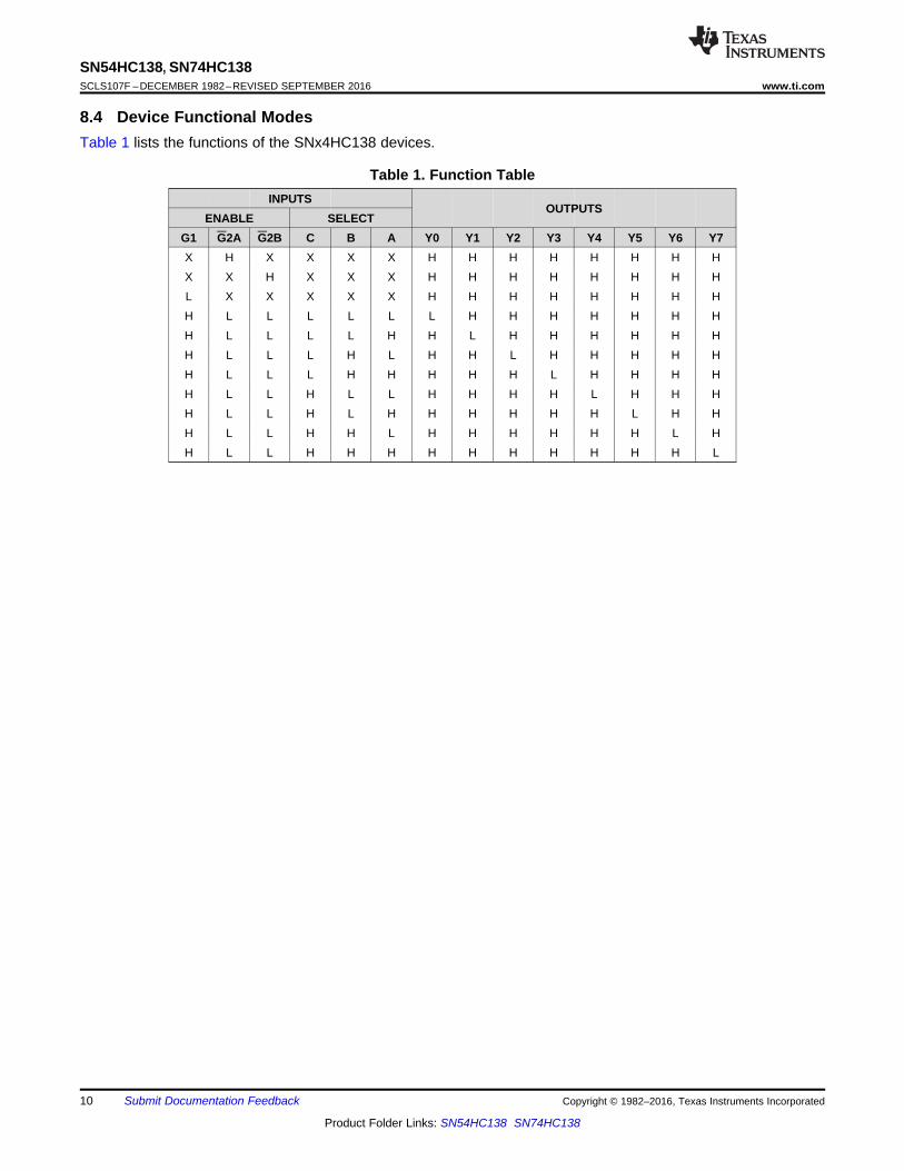
8.4 Device Functional ModesTable 1 lists the functions of the SNx4HC138 devices.
Table 1. Function TableINPUTS
OUTPUTSENABLE SELECT
G1 G2A G2B C B A Y0 Y1 Y2 Y3 Y4 Y5 Y6 Y7X H X X X X H H H H H H H HX X H X X X H H H H H H H HL X X X X X H H H H H H H HH L L L L L L H H H H H H HH L L L L H H L H H H H H HH L L L H L H H L H H H H HH L L L H H H H H L H H H HH L L H L L H H H H L H H HH L L H L H H H H H H L H HH L L H H L H H H H H H L HH L L H H H H H H H H H H L

SN74HC595B
SN74HC138
0V
3.3V
3.3V 0V
SER
SRCLK
RCLK
GPIO Inputs
GPIO Inputs
A
B
C
HIGH
HIGH
HIGH
Y0 Y7
QA
QH
Copyright © 2016, Texas Instruments Incorporated
11
SN54HC138, SN74HC138www.ti.com SCLS107F –DECEMBER 1982–REVISED SEPTEMBER 2016
Product Folder Links: SN54HC138 SN74HC138
Submit Documentation FeedbackCopyright © 1982–2016, Texas Instruments Incorporated
9 Application and Implementation
NOTEInformation in the following applications sections is not part of the TI componentspecification, and TI does not warrant its accuracy or completeness. TI’s customers areresponsible for determining suitability of components for their purposes. Customers shouldvalidate and test their design implementation to confirm system functionality.
9.1 Application InformationThe SN74HC138 is useful as a scanning column selector for an LED Matrix display as it can be used for the lowside drive of the LED string. The decoder functionality ensures that no more than one output is pulled to a low-level logic voltage so that only a single column is enabled at any point in time.
9.2 Typical Application
Figure 4. LED Matrix Driver Application
9.2.1 Design RequirementsThese devices use CMOS technology and have balanced output drive. Take care to avoid bus contentionbecause it can drive currents that would exceed maximum limits. The high drive also creates fast edges into lightloads, so routing and load conditions must be considered to prevent ringing.
9.2.2 Detailed Design Procedure1. Recommended Input Conditions
– For switch time specifications, see propagation delay times in Switching Characteristics.– For input voltage level specifications for control inputs, see VIH and VIL in Electrical Characteristics.
2. Recommended Output Conditions– Outputs must not be pulled above VCC or below GND.
WORST BETTER BEST
1W min.
W
2W
Supply Voltage VCC (V)
Logi
c Le
vel (
V)
2 2.4 2.8 3.2 3.6 4 4.4 4.8 5.2 5.6 60
0.5
1
1.5
2
2.5
3
3.5
4
4.5
5
D002
VIH MINVIL MAX
12
SN54HC138, SN74HC138SCLS107F –DECEMBER 1982–REVISED SEPTEMBER 2016 www.ti.com
Product Folder Links: SN54HC138 SN74HC138
Submit Documentation Feedback Copyright © 1982–2016, Texas Instruments Incorporated
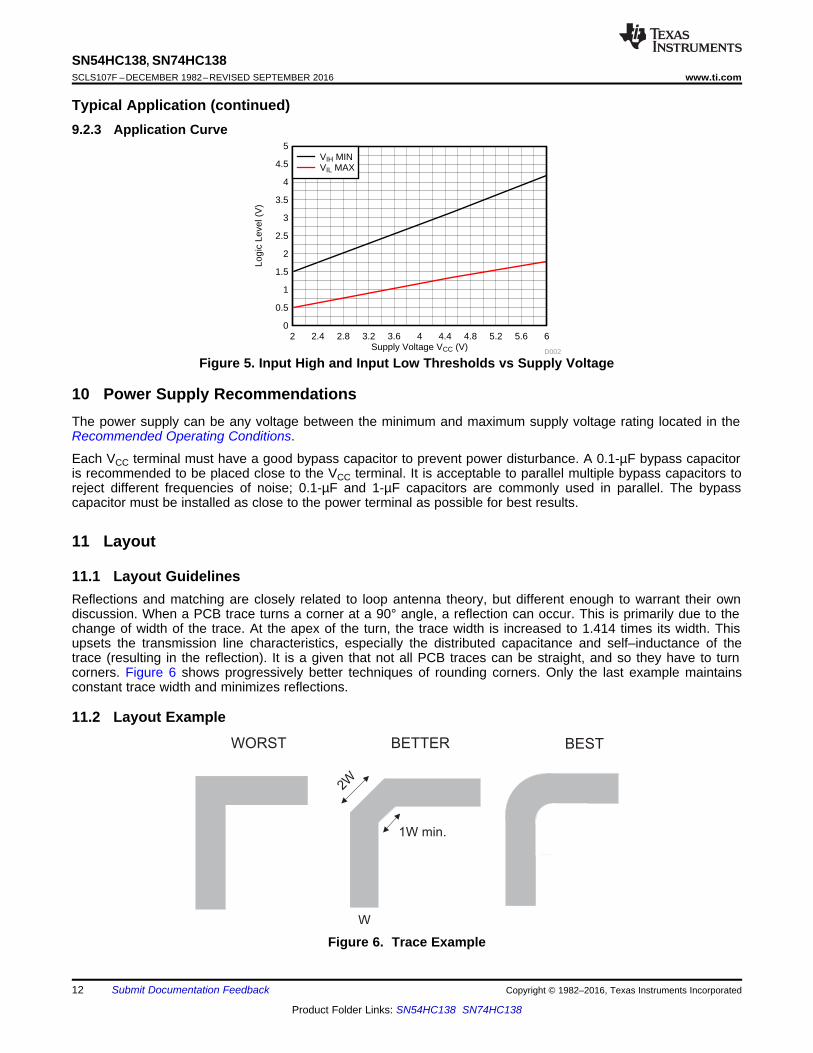
Typical Application (continued)9.2.3 Application Curve
Figure 5. Input High and Input Low Thresholds vs Supply Voltage
10 Power Supply RecommendationsThe power supply can be any voltage between the minimum and maximum supply voltage rating located in theRecommended Operating Conditions.
Each VCC terminal must have a good bypass capacitor to prevent power disturbance. A 0.1-µF bypass capacitoris recommended to be placed close to the VCC terminal. It is acceptable to parallel multiple bypass capacitors toreject different frequencies of noise; 0.1-µF and 1-µF capacitors are commonly used in parallel. The bypasscapacitor must be installed as close to the power terminal as possible for best results.
11 Layout
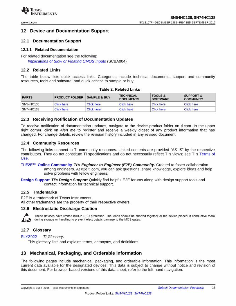
11.1 Layout GuidelinesReflections and matching are closely related to loop antenna theory, but different enough to warrant their owndiscussion. When a PCB trace turns a corner at a 90° angle, a reflection can occur. This is primarily due to thechange of width of the trace. At the apex of the turn, the trace width is increased to 1.414 times its width. Thisupsets the transmission line characteristics, especially the distributed capacitance and self–inductance of thetrace (resulting in the reflection). It is a given that not all PCB traces can be straight, and so they have to turncorners. Figure 6 shows progressively better techniques of rounding corners. Only the last example maintainsconstant trace width and minimizes reflections.
11.2 Layout Example
Figure 6. Trace Example
13
SN54HC138, SN74HC138www.ti.com SCLS107F –DECEMBER 1982–REVISED SEPTEMBER 2016
Product Folder Links: SN54HC138 SN74HC138
Submit Documentation FeedbackCopyright © 1982–2016, Texas Instruments Incorporated
12 Device and Documentation Support
12.1 Documentation Support
12.1.1 Related DocumentationFor related documentation see the following:
Implications of Slow or Floating CMOS Inputs (SCBA004)
12.2 Related LinksThe table below lists quick access links. Categories include technical documents, support and communityresources, tools and software, and quick access to sample or buy.
Table 2. Related Links
PARTS PRODUCT FOLDER SAMPLE & BUY TECHNICALDOCUMENTS
TOOLS &SOFTWARE
SUPPORT &COMMUNITY
SN54HC138 Click here Click here Click here Click here Click hereSN74HC138 Click here Click here Click here Click here Click here
12.3 Receiving Notification of Documentation UpdatesTo receive notification of documentation updates, navigate to the device product folder on ti.com. In the upperright corner, click on Alert me to register and receive a weekly digest of any product information that haschanged. For change details, review the revision history included in any revised document.
12.4 Community ResourcesThe following links connect to TI community resources. Linked contents are provided "AS IS" by the respectivecontributors. They do not constitute TI specifications and do not necessarily reflect TI's views; see TI's Terms ofUse.
TI E2E™ Online Community TI's Engineer-to-Engineer (E2E) Community. Created to foster collaborationamong engineers. At e2e.ti.com, you can ask questions, share knowledge, explore ideas and helpsolve problems with fellow engineers.
Design Support TI's Design Support Quickly find helpful E2E forums along with design support tools andcontact information for technical support.
12.5 TrademarksE2E is a trademark of Texas Instruments.All other trademarks are the property of their respective owners.
12.6 Electrostatic Discharge CautionThese devices have limited built-in ESD protection. The leads should be shorted together or the device placed in conductive foamduring storage or handling to prevent electrostatic damage to the MOS gates.
12.7 GlossarySLYZ022 — TI Glossary.
This glossary lists and explains terms, acronyms, and definitions.
13 Mechanical, Packaging, and Orderable InformationThe following pages include mechanical, packaging, and orderable information. This information is the mostcurrent data available for the designated devices. This data is subject to change without notice and revision ofthis document. For browser-based versions of this data sheet, refer to the left-hand navigation.
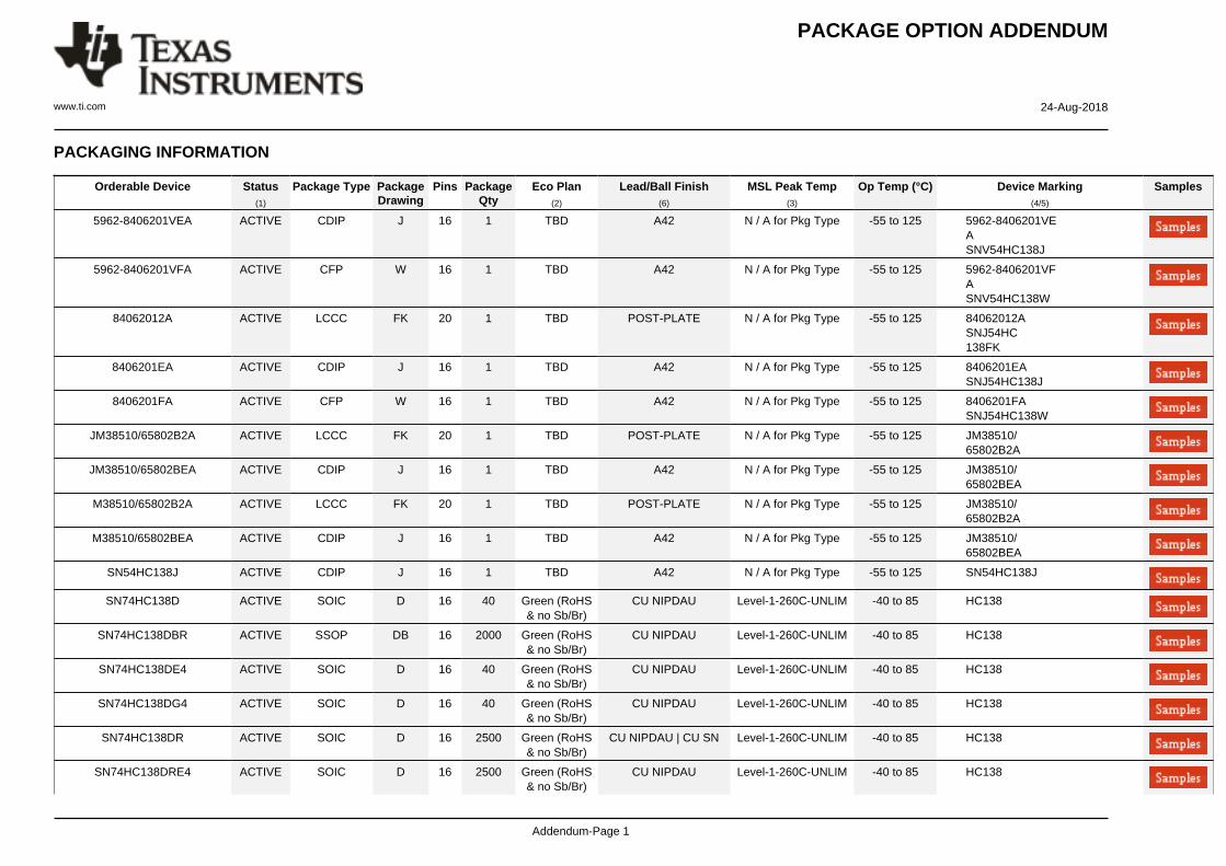
PACKAGE OPTION ADDENDUM
www.ti.com 24-Aug-2018
Addendum-Page 1
PACKAGING INFORMATION
Orderable Device Status(1)
Package Type PackageDrawing
Pins PackageQty
Eco Plan(2)
Lead/Ball Finish(6)
MSL Peak Temp(3)
Op Temp (°C) Device Marking(4/5)
Samples
5962-8406201VEA ACTIVE CDIP J 16 1 TBD A42 N / A for Pkg Type -55 to 125 5962-8406201VEASNV54HC138J
5962-8406201VFA ACTIVE CFP W 16 1 TBD A42 N / A for Pkg Type -55 to 125 5962-8406201VFASNV54HC138W
84062012A ACTIVE LCCC FK 20 1 TBD POST-PLATE N / A for Pkg Type -55 to 125 84062012ASNJ54HC138FK
8406201EA ACTIVE CDIP J 16 1 TBD A42 N / A for Pkg Type -55 to 125 8406201EASNJ54HC138J
8406201FA ACTIVE CFP W 16 1 TBD A42 N / A for Pkg Type -55 to 125 8406201FASNJ54HC138W
JM38510/65802B2A ACTIVE LCCC FK 20 1 TBD POST-PLATE N / A for Pkg Type -55 to 125 JM38510/65802B2A
JM38510/65802BEA ACTIVE CDIP J 16 1 TBD A42 N / A for Pkg Type -55 to 125 JM38510/65802BEA
M38510/65802B2A ACTIVE LCCC FK 20 1 TBD POST-PLATE N / A for Pkg Type -55 to 125 JM38510/65802B2A
M38510/65802BEA ACTIVE CDIP J 16 1 TBD A42 N / A for Pkg Type -55 to 125 JM38510/65802BEA
SN54HC138J ACTIVE CDIP J 16 1 TBD A42 N / A for Pkg Type -55 to 125 SN54HC138J
SN74HC138D ACTIVE SOIC D 16 40 Green (RoHS& no Sb/Br)
CU NIPDAU Level-1-260C-UNLIM -40 to 85 HC138
SN74HC138DBR ACTIVE SSOP DB 16 2000 Green (RoHS& no Sb/Br)
CU NIPDAU Level-1-260C-UNLIM -40 to 85 HC138
SN74HC138DE4 ACTIVE SOIC D 16 40 Green (RoHS& no Sb/Br)
CU NIPDAU Level-1-260C-UNLIM -40 to 85 HC138
SN74HC138DG4 ACTIVE SOIC D 16 40 Green (RoHS& no Sb/Br)
CU NIPDAU Level-1-260C-UNLIM -40 to 85 HC138
SN74HC138DR ACTIVE SOIC D 16 2500 Green (RoHS& no Sb/Br)
CU NIPDAU | CU SN Level-1-260C-UNLIM -40 to 85 HC138
SN74HC138DRE4 ACTIVE SOIC D 16 2500 Green (RoHS& no Sb/Br)
CU NIPDAU Level-1-260C-UNLIM -40 to 85 HC138

PACKAGE OPTION ADDENDUM
www.ti.com 24-Aug-2018
Addendum-Page 2
Orderable Device Status(1)
Package Type PackageDrawing
Pins PackageQty
Eco Plan(2)
Lead/Ball Finish(6)
MSL Peak Temp(3)
Op Temp (°C) Device Marking(4/5)
Samples
SN74HC138DRG4 ACTIVE SOIC D 16 2500 Green (RoHS& no Sb/Br)
CU NIPDAU Level-1-260C-UNLIM -40 to 85 HC138
SN74HC138DT ACTIVE SOIC D 16 250 Green (RoHS& no Sb/Br)
CU NIPDAU Level-1-260C-UNLIM -40 to 85 HC138
SN74HC138N ACTIVE PDIP N 16 25 Green (RoHS& no Sb/Br)
CU NIPDAU | CU SN N / A for Pkg Type -40 to 85 SN74HC138N
SN74HC138NE4 ACTIVE PDIP N 16 25 Green (RoHS& no Sb/Br)
CU NIPDAU N / A for Pkg Type -40 to 85 SN74HC138N
SN74HC138NSR ACTIVE SO NS 16 2000 Green (RoHS& no Sb/Br)
CU NIPDAU Level-1-260C-UNLIM -40 to 85 HC138
SN74HC138PW ACTIVE TSSOP PW 16 90 Green (RoHS& no Sb/Br)
CU NIPDAU Level-1-260C-UNLIM -40 to 85 HC138
SN74HC138PWR ACTIVE TSSOP PW 16 2000 Green (RoHS& no Sb/Br)
CU NIPDAU | CU SN Level-1-260C-UNLIM -40 to 85 HC138
SN74HC138PWRE4 ACTIVE TSSOP PW 16 2000 Green (RoHS& no Sb/Br)
CU NIPDAU Level-1-260C-UNLIM -40 to 85 HC138
SN74HC138PWRG4 ACTIVE TSSOP PW 16 2000 Green (RoHS& no Sb/Br)
CU NIPDAU Level-1-260C-UNLIM -40 to 85 HC138
SN74HC138PWT ACTIVE TSSOP PW 16 250 Green (RoHS& no Sb/Br)
CU NIPDAU Level-1-260C-UNLIM -40 to 85 HC138
SNJ54HC138FK ACTIVE LCCC FK 20 1 TBD POST-PLATE N / A for Pkg Type -55 to 125 84062012ASNJ54HC138FK
SNJ54HC138J ACTIVE CDIP J 16 1 TBD A42 N / A for Pkg Type -55 to 125 8406201EASNJ54HC138J
SNJ54HC138W ACTIVE CFP W 16 1 TBD A42 N / A for Pkg Type -55 to 125 8406201FASNJ54HC138W
(1) The marketing status values are defined as follows:ACTIVE: Product device recommended for new designs.LIFEBUY: TI has announced that the device will be discontinued, and a lifetime-buy period is in effect.NRND: Not recommended for new designs. Device is in production to support existing customers, but TI does not recommend using this part in a new design.PREVIEW: Device has been announced but is not in production. Samples may or may not be available.OBSOLETE: TI has discontinued the production of the device.
PACKAGE OPTION ADDENDUM
www.ti.com 24-Aug-2018
Addendum-Page 3
(2) RoHS: TI defines "RoHS" to mean semiconductor products that are compliant with the current EU RoHS requirements for all 10 RoHS substances, including the requirement that RoHS substancedo not exceed 0.1% by weight in homogeneous materials. Where designed to be soldered at high temperatures, "RoHS" products are suitable for use in specified lead-free processes. TI mayreference these types of products as "Pb-Free".RoHS Exempt: TI defines "RoHS Exempt" to mean products that contain lead but are compliant with EU RoHS pursuant to a specific EU RoHS exemption.Green: TI defines "Green" to mean the content of Chlorine (Cl) and Bromine (Br) based flame retardants meet JS709B low halogen requirements of <=1000ppm threshold. Antimony trioxide basedflame retardants must also meet the <=1000ppm threshold requirement.
(3) MSL, Peak Temp. - The Moisture Sensitivity Level rating according to the JEDEC industry standard classifications, and peak solder temperature.
(4) There may be additional marking, which relates to the logo, the lot trace code information, or the environmental category on the device.
(5) Multiple Device Markings will be inside parentheses. Only one Device Marking contained in parentheses and separated by a "~" will appear on a device. If a line is indented then it is a continuationof the previous line and the two combined represent the entire Device Marking for that device.
(6) Lead/Ball Finish - Orderable Devices may have multiple material finish options. Finish options are separated by a vertical ruled line. Lead/Ball Finish values may wrap to two lines if the finishvalue exceeds the maximum column width.
Important Information and Disclaimer:The information provided on this page represents TI's knowledge and belief as of the date that it is provided. TI bases its knowledge and belief on informationprovided by third parties, and makes no representation or warranty as to the accuracy of such information. Efforts are underway to better integrate information from third parties. TI has taken andcontinues to take reasonable steps to provide representative and accurate information but may not have conducted destructive testing or chemical analysis on incoming materials and chemicals.TI and TI suppliers consider certain information to be proprietary, and thus CAS numbers and other limited information may not be available for release.
In no event shall TI's liability arising out of such information exceed the total purchase price of the TI part(s) at issue in this document sold by TI to Customer on an annual basis.
OTHER QUALIFIED VERSIONS OF SN54HC138, SN54HC138-SP, SN74HC138 :
• Catalog: SN74HC138, SN54HC138
• Automotive: SN74HC138-Q1, SN74HC138-Q1
• Military: SN54HC138
• Space: SN54HC138-SP
NOTE: Qualified Version Definitions:
• Catalog - TI's standard catalog product
PACKAGE OPTION ADDENDUM
www.ti.com 24-Aug-2018
Addendum-Page 4
• Automotive - Q100 devices qualified for high-reliability automotive applications targeting zero defects
• Military - QML certified for Military and Defense Applications
• Space - Radiation tolerant, ceramic packaging and qualified for use in Space-based application
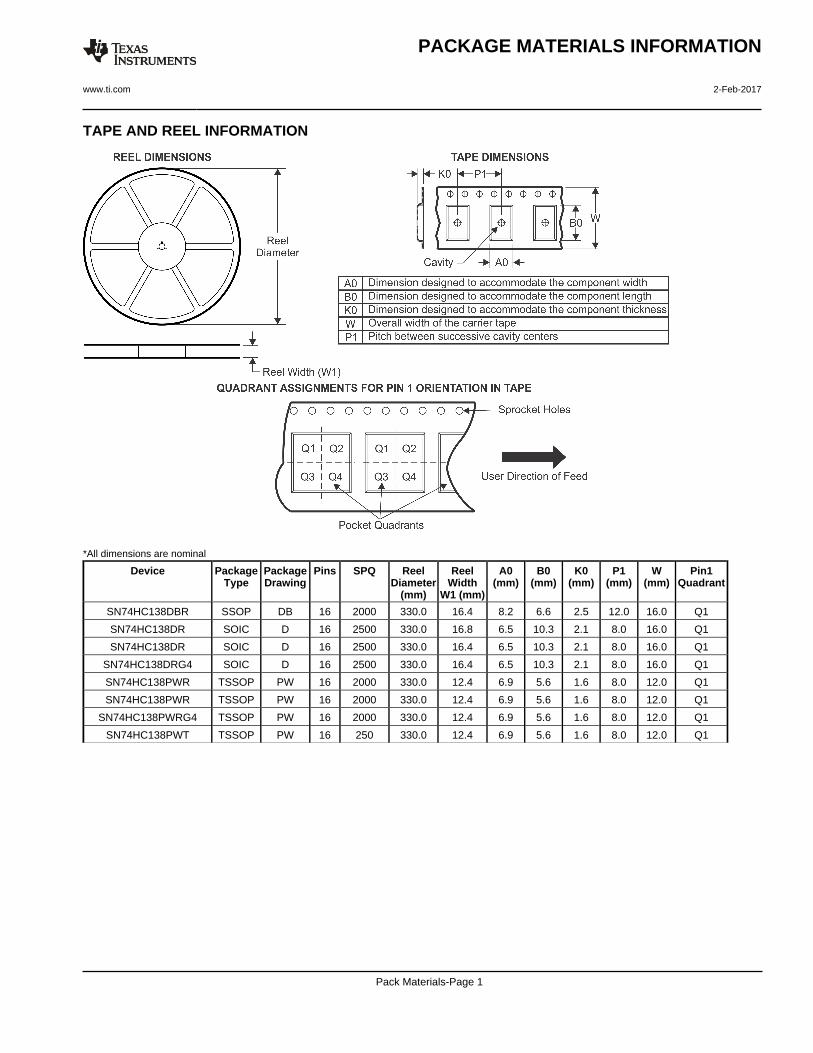
TAPE AND REEL INFORMATION
*All dimensions are nominal
Device PackageType
PackageDrawing
Pins SPQ ReelDiameter
(mm)
ReelWidth
W1 (mm)
A0(mm)
B0(mm)
K0(mm)
P1(mm)
W(mm)
Pin1Quadrant
SN74HC138DBR SSOP DB 16 2000 330.0 16.4 8.2 6.6 2.5 12.0 16.0 Q1
SN74HC138DR SOIC D 16 2500 330.0 16.8 6.5 10.3 2.1 8.0 16.0 Q1
SN74HC138DR SOIC D 16 2500 330.0 16.4 6.5 10.3 2.1 8.0 16.0 Q1
SN74HC138DRG4 SOIC D 16 2500 330.0 16.4 6.5 10.3 2.1 8.0 16.0 Q1
SN74HC138PWR TSSOP PW 16 2000 330.0 12.4 6.9 5.6 1.6 8.0 12.0 Q1
SN74HC138PWR TSSOP PW 16 2000 330.0 12.4 6.9 5.6 1.6 8.0 12.0 Q1
SN74HC138PWRG4 TSSOP PW 16 2000 330.0 12.4 6.9 5.6 1.6 8.0 12.0 Q1
SN74HC138PWT TSSOP PW 16 250 330.0 12.4 6.9 5.6 1.6 8.0 12.0 Q1
PACKAGE MATERIALS INFORMATION
www.ti.com 2-Feb-2017
Pack Materials-Page 1
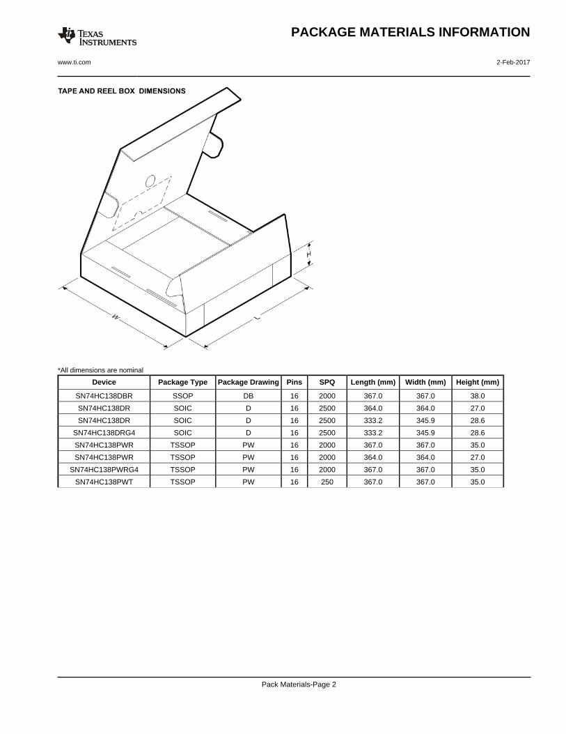
*All dimensions are nominal
Device Package Type Package Drawing Pins SPQ Length (mm) Width (mm) Height (mm)
SN74HC138DBR SSOP DB 16 2000 367.0 367.0 38.0
SN74HC138DR SOIC D 16 2500 364.0 364.0 27.0
SN74HC138DR SOIC D 16 2500 333.2 345.9 28.6
SN74HC138DRG4 SOIC D 16 2500 333.2 345.9 28.6
SN74HC138PWR TSSOP PW 16 2000 367.0 367.0 35.0
SN74HC138PWR TSSOP PW 16 2000 364.0 364.0 27.0
SN74HC138PWRG4 TSSOP PW 16 2000 367.0 367.0 35.0
SN74HC138PWT TSSOP PW 16 250 367.0 367.0 35.0
PACKAGE MATERIALS INFORMATION
www.ti.com 2-Feb-2017
Pack Materials-Page 2
MECHANICAL DATA
MSSO002E – JANUARY 1995 – REVISED DECEMBER 2001
POST OFFICE BOX 655303 • DALLAS, TEXAS 75265
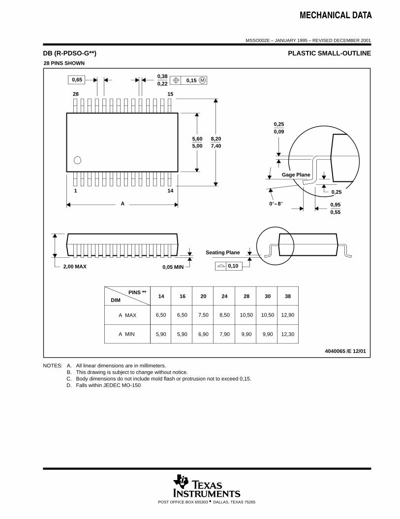
DB (R-PDSO-G**) PLASTIC SMALL-OUTLINE
4040065 /E 12/01
28 PINS SHOWN
Gage Plane
8,207,40
0,550,95
0,25
38
12,90
12,30
28
10,50
24
8,50
Seating Plane
9,907,90
30
10,50
9,90
0,38
5,605,00
15
0,22
14
A
28
1
2016
6,506,50
14
0,05 MIN
5,905,90
DIM
A MAX
A MIN
PINS **
2,00 MAX
6,90
7,50
0,65 M0,15
0°–8°
0,10
0,090,25
NOTES: A. All linear dimensions are in millimeters.B. This drawing is subject to change without notice.C. Body dimensions do not include mold flash or protrusion not to exceed 0,15.D. Falls within JEDEC MO-150
IMPORTANT NOTICE
Texas Instruments Incorporated (TI) reserves the right to make corrections, enhancements, improvements and other changes to itssemiconductor products and services per JESD46, latest issue, and to discontinue any product or service per JESD48, latest issue. Buyersshould obtain the latest relevant information before placing orders and should verify that such information is current and complete.TI’s published terms of sale for semiconductor products (http://www.ti.com/sc/docs/stdterms.htm) apply to the sale of packaged integratedcircuit products that TI has qualified and released to market. Additional terms may apply to the use or sale of other types of TI products andservices.Reproduction of significant portions of TI information in TI data sheets is permissible only if reproduction is without alteration and isaccompanied by all associated warranties, conditions, limitations, and notices. TI is not responsible or liable for such reproduceddocumentation. Information of third parties may be subject to additional restrictions. Resale of TI products or services with statementsdifferent from or beyond the parameters stated by TI for that product or service voids all express and any implied warranties for theassociated TI product or service and is an unfair and deceptive business practice. TI is not responsible or liable for any such statements.Buyers and others who are developing systems that incorporate TI products (collectively, “Designers”) understand and agree that Designersremain responsible for using their independent analysis, evaluation and judgment in designing their applications and that Designers havefull and exclusive responsibility to assure the safety of Designers' applications and compliance of their applications (and of all TI productsused in or for Designers’ applications) with all applicable regulations, laws and other applicable requirements. Designer represents that, withrespect to their applications, Designer has all the necessary expertise to create and implement safeguards that (1) anticipate dangerousconsequences of failures, (2) monitor failures and their consequences, and (3) lessen the likelihood of failures that might cause harm andtake appropriate actions. Designer agrees that prior to using or distributing any applications that include TI products, Designer willthoroughly test such applications and the functionality of such TI products as used in such applications.TI’s provision of technical, application or other design advice, quality characterization, reliability data or other services or information,including, but not limited to, reference designs and materials relating to evaluation modules, (collectively, “TI Resources”) are intended toassist designers who are developing applications that incorporate TI products; by downloading, accessing or using TI Resources in anyway, Designer (individually or, if Designer is acting on behalf of a company, Designer’s company) agrees to use any particular TI Resourcesolely for this purpose and subject to the terms of this Notice.TI’s provision of TI Resources does not expand or otherwise alter TI’s applicable published warranties or warranty disclaimers for TIproducts, and no additional obligations or liabilities arise from TI providing such TI Resources. TI reserves the right to make corrections,enhancements, improvements and other changes to its TI Resources. TI has not conducted any testing other than that specificallydescribed in the published documentation for a particular TI Resource.Designer is authorized to use, copy and modify any individual TI Resource only in connection with the development of applications thatinclude the TI product(s) identified in such TI Resource. NO OTHER LICENSE, EXPRESS OR IMPLIED, BY ESTOPPEL OR OTHERWISETO ANY OTHER TI INTELLECTUAL PROPERTY RIGHT, AND NO LICENSE TO ANY TECHNOLOGY OR INTELLECTUAL PROPERTYRIGHT OF TI OR ANY THIRD PARTY IS GRANTED HEREIN, including but not limited to any patent right, copyright, mask work right, orother intellectual property right relating to any combination, machine, or process in which TI products or services are used. Informationregarding or referencing third-party products or services does not constitute a license to use such products or services, or a warranty orendorsement thereof. Use of TI Resources may require a license from a third party under the patents or other intellectual property of thethird party, or a license from TI under the patents or other intellectual property of TI.TI RESOURCES ARE PROVIDED “AS IS” AND WITH ALL FAULTS. TI DISCLAIMS ALL OTHER WARRANTIES ORREPRESENTATIONS, EXPRESS OR IMPLIED, REGARDING RESOURCES OR USE THEREOF, INCLUDING BUT NOT LIMITED TOACCURACY OR COMPLETENESS, TITLE, ANY EPIDEMIC FAILURE WARRANTY AND ANY IMPLIED WARRANTIES OFMERCHANTABILITY, FITNESS FOR A PARTICULAR PURPOSE, AND NON-INFRINGEMENT OF ANY THIRD PARTY INTELLECTUALPROPERTY RIGHTS. TI SHALL NOT BE LIABLE FOR AND SHALL NOT DEFEND OR INDEMNIFY DESIGNER AGAINST ANY CLAIM,INCLUDING BUT NOT LIMITED TO ANY INFRINGEMENT CLAIM THAT RELATES TO OR IS BASED ON ANY COMBINATION OFPRODUCTS EVEN IF DESCRIBED IN TI RESOURCES OR OTHERWISE. IN NO EVENT SHALL TI BE LIABLE FOR ANY ACTUAL,DIRECT, SPECIAL, COLLATERAL, INDIRECT, PUNITIVE, INCIDENTAL, CONSEQUENTIAL OR EXEMPLARY DAMAGES INCONNECTION WITH OR ARISING OUT OF TI RESOURCES OR USE THEREOF, AND REGARDLESS OF WHETHER TI HAS BEENADVISED OF THE POSSIBILITY OF SUCH DAMAGES.Unless TI has explicitly designated an individual product as meeting the requirements of a particular industry standard (e.g., ISO/TS 16949and ISO 26262), TI is not responsible for any failure to meet such industry standard requirements.Where TI specifically promotes products as facilitating functional safety or as compliant with industry functional safety standards, suchproducts are intended to help enable customers to design and create their own applications that meet applicable functional safety standardsand requirements. Using products in an application does not by itself establish any safety features in the application. Designers mustensure compliance with safety-related requirements and standards applicable to their applications. Designer may not use any TI products inlife-critical medical equipment unless authorized officers of the parties have executed a special contract specifically governing such use.Life-critical medical equipment is medical equipment where failure of such equipment would cause serious bodily injury or death (e.g., lifesupport, pacemakers, defibrillators, heart pumps, neurostimulators, and implantables). Such equipment includes, without limitation, allmedical devices identified by the U.S. Food and Drug Administration as Class III devices and equivalent classifications outside the U.S.TI may expressly designate certain products as completing a particular qualification (e.g., Q100, Military Grade, or Enhanced Product).Designers agree that it has the necessary expertise to select the product with the appropriate qualification designation for their applicationsand that proper product selection is at Designers’ own risk. Designers are solely responsible for compliance with all legal and regulatoryrequirements in connection with such selection.Designer will fully indemnify TI and its representatives against any damages, costs, losses, and/or liabilities arising out of Designer’s non-compliance with the terms and provisions of this Notice.
Mailing Address: Texas Instruments, Post Office Box 655303, Dallas, Texas 75265Copyright © 2018, Texas Instruments Incorporated


![ProLight PBVC-10FWU-F3G 10W Power LED Version: 1EV External Visual JESD22 B-101 N/A See notes [2] 0 HTFB High Temperature Forward Bias JESD22-A108 Tamb =85 C, IF = max. DC [1] 1000](https://static.fdocuments.us/doc/165x107/6127a9601ad5444e340186c0/prolight-pbvc-10fwu-f3g-10w-power-led-version-1-ev-external-visual-jesd22-b-101.jpg)