74HCT9046A PLL with band gap controlled VCOdocs-europe.electrocomponents.com/webdocs/0423/... · n...
43
1. General description The 74HCT9046A is a high-speed Si-gate CMOS device. It is specified in compliance with JEDEC standard no 7A. 2. Features ■ Operation power supply voltage range from 4.5 V to 5.5 V ■ Low power consumption ■ Inhibit control for ON/OFF keying and for low standby power consumption ■ center frequency up to 17 MHz (typical) at V CC = 5.5 V ■ Choice of two phase comparators: ◆ PC1: EXCLUSIVE-OR ◆ PC2: Edge-triggered JK flip-flop ■ No dead zone of PC2 ■ Charge pump output on PC2, whose current is set by an external resistor R bias ■ center frequency tolerance ±10 % ■ Excellent Voltage Controlled Oscillator (VCO) linearity ■ Low frequency drift with supply voltage and temperature variations ■ On-chip band gap reference ■ Glitch free operation of VCO, even at very low frequencies ■ Zero voltage offset due to operational amplifier buffering ■ ESD protection: ◆ HBM JESD22-A114F exceeds 2000 V ◆ MM JESD22-A115-A exceeds 200 V 74HCT9046A PLL with band gap controlled VCO Rev. 06 — 15 September 2009 Product data sheet
-
Upload
vuongthuan -
Category
Documents
-
view
218 -
download
3
Transcript of 74HCT9046A PLL with band gap controlled VCOdocs-europe.electrocomponents.com/webdocs/0423/... · n...
1. General description
The 74HCT9046A is a high-speed Si-gate CMOS device. It is specified in compliance withJEDEC standard no 7A.
2. Features
n Operation power supply voltage range from 4.5 V to 5.5 V
n Low power consumption
n Inhibit control for ON/OFF keying and for low standby power consumption
n center frequency up to 17 MHz (typical) at VCC = 5.5 V
n Choice of two phase comparators:
u PC1: EXCLUSIVE-OR
u PC2: Edge-triggered JK flip-flop
n No dead zone of PC2
n Charge pump output on PC2, whose current is set by an external resistor Rbias
n center frequency tolerance ±10 %
n Excellent Voltage Controlled Oscillator (VCO) linearity
n Low frequency drift with supply voltage and temperature variations
n On-chip band gap reference
n Glitch free operation of VCO, even at very low frequencies
n Zero voltage offset due to operational amplifier buffering
n ESD protection:
u HBM JESD22-A114F exceeds 2000 V
u MM JESD22-A115-A exceeds 200 V
74HCT9046APLL with band gap controlled VCORev. 06 — 15 September 2009 Product data sheet
NXP Semiconductors 74HCT9046APLL with band gap controlled VCO
3. Applications
n FM modulation and demodulation where a small center frequency tolerance isessential
n Frequency synthesis and multiplication where a low jitter is required (e.g. videopicture-in-picture)
n Frequency discrimination
n Tone decoding
n Data synchronization and conditioning
n Voltage-to-frequency conversion
n Motor-speed control
4. Ordering information
Table 1. Ordering information
Type number Package
Temperature range Name Description Version
74HCT9046AN −40 °C to +125 °C DIP16 plastic dual in-line package; 16 leads (300 mil) SOT38-4
74HCT9046AD −40 °C to +125 °C SO16 plastic small outline package; 16 leads; body width3.9 mm
SOT109-1
74HCT9046APW −40 °C to +125 °C TSSOP16 plastic thin shrink small outline package; 16 leads;body width 4.4 mm
SOT403-1
74HCT9046A_6 © NXP B.V. 2009. All rights reserved.
Product data sheet Rev. 06 — 15 September 2009 2 of 43
NXP Semiconductors 74HCT9046APLL with band gap controlled VCO
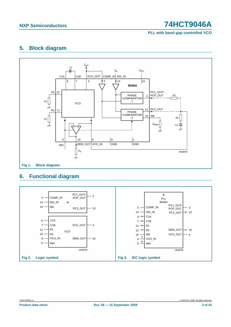
5. Block diagram
6. Functional diagram
Fig 1. Block diagram
PHASECOMPARATOR
2
13
PHASECOMPARATOR
1
2
15
SIG_INCOMP_INC1A C1B
fout
fin VCC
DEM_OUTINH VCO_IN
R2
12
11
3 14 16476
5 10 9
GND
8
GND
1
C1
9046A
VCO
Rs
R1R4
R3
C2
PC2_OUT
mbd040
PC1_OUT/PCP_OUT
VCO_OUT
R2
R1
RB
Rbias
Fig 2. Logic symbol Fig 3. IEC logic symbol
mbd038
PC1_OUT/PCP_OUT
VCO_OUT
C1A
C1B
VCO_IN DEM_OUT
R2
R1
SIG_IN
INH
VCO
6
7
11
12
9
5
4
10
2
13
3
14
15PC2_OUT
Φ
COMP_IN
RB
mbd039
SIG_IN
INH
6
7
11
12
9
5
4
10
2
13
3
14
15
Φ
COMP_IN
PLL9046A
PC1_OUT/PCP_OUT
VCO_OUT
C1A
C1B
VCO_IN
DEM_OUTR2
R1
PC2_OUT
RB
74HCT9046A_6 © NXP B.V. 2009. All rights reserved.
Product data sheet Rev. 06 — 15 September 2009 3 of 43
xxxxxxxxxxxxxxxxxxxxx xxxxxxxxxxxxxxxxxxxxxxxxxx xxxxxxx x x x xxxxxxxxxxxxxxxxxxxxxxxxxxxxxx xxxxxxxxxxxxxxxxxxx xx xxxxxxx xxxxxxxxxxxxxxxxxxxxxxxxxxx xxxxxxxxxxxxxxxxxxx xxxxxx xxxxxxxxxxxxxxxxxxxxxxxxxxxxxxxxxxx xxxxxxxxxxxx x xxxxxxxxxxxxxxxxxxxxxx xxxxxxxxxxxxxxxxxxxxxxxxxxxxxx xxxxx xxxxxxxxxxxxxxxxxxxxxxxxxxxxxxxxxxxxxxxxxxxxxxxxxx xxxxxxxxxxxxxxxxxxxxxxxxxxxxxxxxx xxxxxxxxxxxxxxxxxxxx xxx
74HC
T9046A
_6
Product data shee
NX
P S
emiconductors
74HC
T9046A
PLL w
ith band gap controlled VC
O
mbd102
PC1_OUT/PCP_OUT
PC2_OUT
Rbias
RB
C2
R4
2
13
R3
15
COMP_IN SIG_IN
3 14
VCO_OUTC1BC1A
76 4
C1fout fin
R3' = Rbias /17
R3'(1)
(1)
© N
XP
B.V. 2009. A
ll rights reserved.
tR
ev. 06 — 15 S
eptember 2009
4 of 43
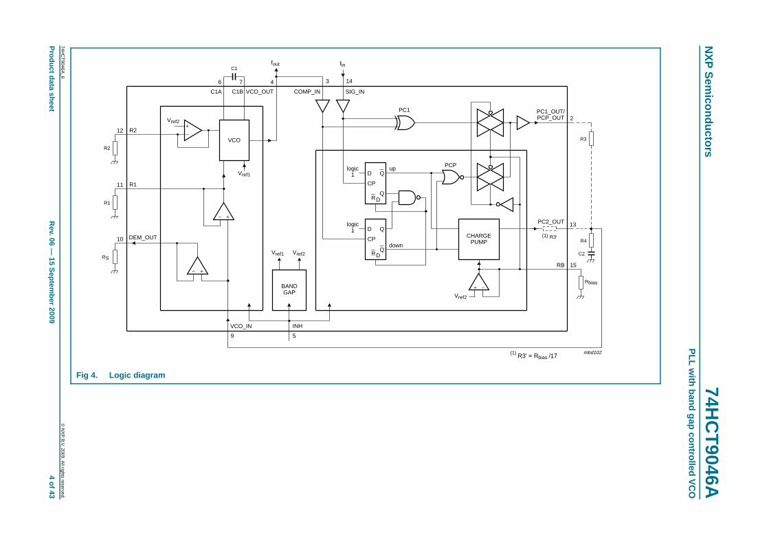
Fig 4. Logic diagram
PCPD Q
CP
QRD
logic1
D Q
CP
QRD
logic1
down
up
CHARGEPUMP
Vref2
Vref2
Vref2
Vref1
Vref1
PC1
BANDGAP
5
INH
9
VCO
DEM_OUT
12
R2
11
R1
10
RS
R2
R1
VCO_IN
NXP Semiconductors 74HCT9046APLL with band gap controlled VCO
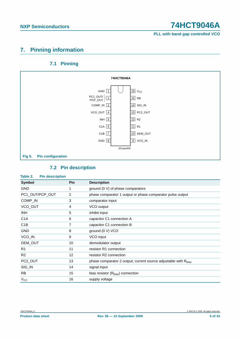
7. Pinning information
7.1 Pinning
7.2 Pin description
Fig 5. Pin configuration
PC1_OUT/PCP_OUT
GND VCC
RB
COMP_IN SIG_IN
VCO_OUT PC2_OUT
INH R2
C1A R1
C1B DEM_OUT
GND VCO_IN
001aae500
1
2
3
4
5
6
7
8
10
9
12
11
14
13
16
15
74HCT9046A
Table 2. Pin description
Symbol Pin Description
GND 1 ground (0 V) of phase comparators
PC1_OUT/PCP_OUT 2 phase comparator 1 output or phase comparator pulse output
COMP_IN 3 comparator input
VCO_OUT 4 VCO output
INH 5 inhibit input
C1A 6 capacitor C1 connection A
C1B 7 capacitor C1 connection B
GND 8 ground (0 V) VCO
VCO_IN 9 VCO input
DEM_OUT 10 demodulator output
R1 11 resistor R1 connection
R2 12 resistor R2 connection
PC2_OUT 13 phase comparator 2 output; current source adjustable with Rbias
SIG_IN 14 signal input
RB 15 bias resistor (Rbias) connection
VCC 16 supply voltage
74HCT9046A_6 © NXP B.V. 2009. All rights reserved.
Product data sheet Rev. 06 — 15 September 2009 5 of 43

NXP Semiconductors 74HCT9046APLL with band gap controlled VCO
8. Functional description
The 74HCT9046A is a phase-locked-loop circuit that comprises a linear VCO and twodifferent phase comparators (PC1 and PC2) with a common signal input amplifier and acommon comparator input, see Figure 1. The signal input can be directly coupled to largevoltage signals (CMOS level), or indirectly coupled (with a series capacitor) to smallvoltage signals. A self-bias input circuit keeps small voltage signals within the linear regionof the input amplifiers. With a passive low-pass filter, the 74HCT9046A forms asecond-order loop PLL.
The principle of this phase-locked-loop is based on the familiar 74HCT4046A. Howeverextra features are built-in, allowing very high-performance phase-locked-loop applications.This is done, at the expense of PC3, which is skipped in this 74HCT9046A. The PC2 isequipped with a current source output stage here. Further a band gap is applied for allinternal references, allowing a small center frequency tolerance. The details are summedup in Section 8.1. If one is familiar with the 74HCT4046A already, it will do to read thissection only.
8.1 Differences with respect to the familiar 74HCT4046A
• A center frequency tolerance of maximum ±10 %.
• The on board band gap sets the internal references resulting in a minimal frequencyshift at supply voltage variations and temperature variations.
• The value of the frequency offset is determined by an internal reference voltage of2.5 V instead of VCC − 0.7 V; In this way the offset frequency will not shift over thesupply voltage range.
• A current switch charge pump output on pin PC2_OUT allows a virtually idealperformance of PC2; The gain of PC2 is independent of the voltage across thelow-pass filter; Further a passive low-pass filter in the loop achieves an activeperformance. The influence of the parasitic capacitance of the PC2 output plays norole here, resulting in a true correspondence of the output correction pulse and thephase difference even up to phase differences as small as a few nanoseconds.
• Because of its linear performance without dead zone, higher impedance values for thefilter, hence lower C-values, can be chosen; correct operation will not be influenced byparasitic capacitances as in case of the voltage source output using the74HCT4046A.
• No PC3 on pin RB but instead a resistor connected to GND, which sets theload/unload currents of the charge pump (PC2).
• Extra GND pin 1 to allow an excellent FM demodulator performance even at 10 MHzand higher.
• Combined function of pin PC1_OUT/PCP_OUT. If pin RB is connected to VCC (nobias resistor Rbias) pin PC1_OUT/PCP_OUT has its familiar function viz. output ofPC1. If at pin RB a resistor (Rbias) is connected to GND it is assumed that PC2 hasbeen chosen as phase comparator. Connection of Rbias is sensed by internal circuitryand this changes the function of pin PC1_OUT/PCP_OUT into a lock detect output(PCP_OUT) with the same characteristics as PCP_OUT of pin 1 of the 74HCT4046A.
74HCT9046A_6 © NXP B.V. 2009. All rights reserved.
Product data sheet Rev. 06 — 15 September 2009 6 of 43

NXP Semiconductors 74HCT9046APLL with band gap controlled VCO
• The inhibit function differs. For the 74HCT4046A a HIGH-level at the inhibit input(pin INH) disables the VCO and demodulator, while a LOW-level turns both on. Forthe 74HCT9046A a HIGH-level on the inhibit input disables the whole circuit tominimize standby power consumption.
8.2 VCOThe VCO requires one external capacitor C1 (between pins C1A and C1B) and oneexternal resistor R1 (between pins R1 and GND) or two external resistors R1 and R2(between pins R1 and GND, and R2 and GND). Resistor R1 and capacitor C1 determinethe frequency range of the VCO. Resistor R2 enables the VCO to have a frequency offsetif required (see Figure 4).
The high input impedance of the VCO simplifies the design of the low-pass filters by givingthe designer a wide choice of resistor/capacitor ranges. In order not to load the low-passfilter, a demodulator output of the VCO input voltage is provided at pin DEM_OUT. TheDEM_OUT voltage equals that of the VCO input. If DEM_OUT is used, a series resistor(Rs) should be connected from pin DEM_OUT to GND; if unused, DEM_OUT should beleft open. The VCO output (pin VCO_OUT) can be connected directly to the comparatorinput (pin COMP_IN), or connected via a frequency divider. The output signal has a dutycycle of 50 % (maximum expected deviation 1 %), if the VCO input is held at a constantDC level. A LOW-level at the inhibit input (pin INH) enables the VCO and demodulator,while a HIGH-level turns both off to minimize standby power consumption.
8.3 Phase comparatorsThe signal input (pin SIG_IN) can be directly coupled to the self-biasing amplifier atpin SIG_IN, provided that the signal swing is between the standard HC family input logiclevels. Capacitive coupling is required for signals with smaller swings.
8.3.1 Phase Comparator 1 (PC1)
This circuit is an EXCLUSIVE-OR network. The signal and comparator input frequencies(fi) must have a 50 % duty cycle to obtain the maximum locking range. The transfercharacteristic of PC1, assuming ripple (fr = 2fi) is suppressed, is:
where:
VDEM_OUT is the demodulator output at pin DEM_OUT
VDEM_OUT = VPC1_OUT (via low-pass)
The phase comparator gain is:
The average output voltage from PC1, fed to the VCO input via the low-pass filter andseen at the demodulator output at pin DEM_OUT (VDEM_OUT), is the resultant of the phasedifferences of signals (SIG_IN) and the comparator input (COMP_IN) as shown inFigure 6. The average of VDEM_OUT is equal to 0.5VCC when there is no signal or noise atSIG_IN and with this input the VCO oscillates at the center frequency (f0). Typical
VDEM_OUT
VCC
π---------- ΦSIG_IN ΦCOMP_IN–( )=
K p
VCC
π---------- V r⁄( )=
74HCT9046A_6 © NXP B.V. 2009. All rights reserved.
Product data sheet Rev. 06 — 15 September 2009 7 of 43

NXP Semiconductors 74HCT9046APLL with band gap controlled VCO
waveforms for the PC1 loop locked at f0 are shown in Figure 7. This figure also shows theactual waveforms across the VCO capacitor at pins C1A and C1B (VC1A and VC1B) toshow the relation between these ramps and the VCO_OUT voltage.
The frequency capture range (2f0) is defined as the frequency range of input signals onwhich the PLL will lock if it was initially out-of-lock. The frequency lock range (2fL) isdefined as the frequency range of the input signals on which the loop will stay locked if itwas initially in lock. The capture range is smaller or equal to the lock range.
With PC1, the capture range depends on the low-pass filter characteristics and can bemade as large as the lock range. This configuration remains locked even with very noisyinput signals. Typical behavior of this type of phase comparator is that it may lock to inputfrequencies close to the harmonics of the VCO center frequency.
Fig 6. Phase comparator 1; average output voltage as a function of input phasedifference
mbd101
180o0 o 90 o
0.5VCC
0
VCC
VDEM_OUT(AV)
ΦPC_IN
VDEM_OUT VPCI_OUT
VCC
π-----------ΦSIG_IN ΦCOMP_IN–= =
ΦPC_IN ΦSIG_IN ΦCOMP_IN–( )=
74HCT9046A_6 © NXP B.V. 2009. All rights reserved.
Product data sheet Rev. 06 — 15 September 2009 8 of 43

NXP Semiconductors 74HCT9046APLL with band gap controlled VCO
8.3.2 Phase Comparator 2 (PC2)
This is a positive edge-triggered phase and frequency detector. When the PLL is usingthis comparator, the loop is controlled by positive signal transitions and the duty cycles ofSIG_IN and COMP_IN are not important. PC2 comprises two D-type flip-flops, controlgating and a 3-state output stage with sink and source transistors acting as currentsources, henceforth called charge pump output of PC2. The circuit functions as anup-down counter (see Figure 4) where SIG_IN causes an up-count and COMP_IN a downcount. The current switch charge pump output allows a virtually ideal performance of PC2,due to appliance of some pulse overlap of the up and down signals, see Figure 8a.
The pump current Icp is independent from the supply voltage and is set by the internalband gap reference of 2.5 V.
Where Rbias is the external bias resistor between pin RB and ground.
The current and voltage transfer function of PC2 are shown in Figure 9.
The phase comparator gain is:
Fig 7. Typical waveforms for PLL using phase comparator 1; loop-locked at f 0
mbd100
PC1_OUT
VCO_INVCC
GND
VCO_OUT
COMP_IN
SIGN_IN
C1A
C1B
VC1A
VC1B
I cp 172.5
Rbias------------ A( )×=
KP
I cp
2π---------- A r⁄( )=
74HCT9046A_6 © NXP B.V. 2009. All rights reserved.
Product data sheet Rev. 06 — 15 September 2009 9 of 43

NXP Semiconductors 74HCT9046APLL with band gap controlled VCO
When the frequencies of SIG_IN and COMP_IN are equal but the phase of SIG_IN leadsthat of COMP_IN, the up output driver at PC2_OUT is held ‘ON’ for a time correspondingto the phase difference (ΦPC_IN). When the phase of SIG_IN lags that of COMP_IN, thedown or sink driver is held ‘ON’.
a. At every ∆Φ, even at zero ∆Φ both switches areclosed simultaneously for a short period (typically15 ns).
b. Comparable voltage-controlled switch
Fig 8. The current switch charge pump output of PC2
mbd046
PC2_OUT
C2
VCC
Icp
Icp
down
up
∆ Φ = ΦPC_IN
pulse overlap of approximately 15 ns mbd099
R3'
Icp
up
down C2
VCC
PC2_OUT
VC2_OUT
a. Current transfer b. Voltage transfer. This transfer can be observed atPC2_OUT by connecting a resistor (R = 10 kΩ)between PC2_OUT and 0.5VCC.
Fig 9. Phase comparator 2 current and voltage transfer characteristics
001aak442
0
0ΦPC_IN
+Icp
−Icp
−2π +2π
001aak443
0
0.5VCC
0
VCC
VDEM_OUT(AV)Icp × R
ΦPC_IN−2π +2π
pumpcurrentI cp
2π----------ΦPC_INVDEM_OUT V=
PC2_OUT5
4π------ΦPC_IN=
ΦPC_IN ΦSIG_IN ΦCOMP_IN–( )=
74HCT9046A_6 © NXP B.V. 2009. All rights reserved.
Product data sheet Rev. 06 — 15 September 2009 10 of 43

NXP Semiconductors 74HCT9046APLL with band gap controlled VCO
When the frequency of SIG_IN is higher than that of COMP_IN, the source output driver isheld ‘ON’ for most of the input signal cycle time and for the remainder of the cycle timeboth drivers are ‘OFF’ (3-state). If the SIG_IN frequency is lower than the COMP_INfrequency, then it is the sink driver that is held ‘ON’ for most of the cycle. Subsequently thevoltage at the capacitor (C2) of the low-pass filter connected to PC2_OUT varies until thesignal and comparator inputs are equal in both phase and frequency. At this stable pointthe voltage on C2 remains constant as the PC2 output is in 3-state and the VCO input atpin 9 is a high-impedance. Also in this condition the signal at the phase comparator pulseoutput (PCP_OUT) has a minimum output pulse width equal to the overlap time, so can beused for indicating a locked condition.
Thus for PC2 no phase difference exists between SIG_IN and COMP_IN over the fullfrequency range of the VCO. Moreover, the power dissipation due to the low-pass filter isreduced because both output drivers are OFF for most of the signal input cycle. It shouldbe noted that the PLL lock range for this type of phase comparator is equal to the capturerange and is independent of the low-pass filter. With no signal present at SIG_IN the VCOadjust, via PC2, to its lowest frequency.
By using current sources as charge pump output on PC2, the dead zone or backlash timecould be reduced to zero. Also, the pulse widening due to the parasitic output capacitanceplays no role here. This enables a linear transfer function, even in the vicinity of the zerocrossing. The differences between a voltage switch charge pump and a current switchcharge pump are shown in Figure 11.
The pulse overlap of the up and down signals (typically 15 ns).
Fig 10. Timing diagram for PC2
mbd047
SIG_IN
COMP_IN
VCO_OUT
high-impedance OFF-state,(zero current)
15 ns typicalUP
DOWN
CURRENT ATPC2_OUT
PC2_OUT/VCO_IN
PCP_OUT
PC_IN
74HCT9046A_6 © NXP B.V. 2009. All rights reserved.
Product data sheet Rev. 06 — 15 September 2009 11 of 43

NXP Semiconductors 74HCT9046APLL with band gap controlled VCO
The design of the low-pass filter is somewhat different when using current sources. Theexternal resistor R3 is no longer present when using PC2 as phase comparator.The current source is set by Rbias. A simple capacitor behaves as an ideal integrator now,because the capacitor is charged by a constant current. The transfer function of thevoltage switch charge pump may be used. In fact it is even more valid, because thetransfer function is no longer restricted for small changes only. Further the current isindependent from both the supply voltage and the voltage across the filter. For one that isfamiliar with the low-pass filter design of the 74HCT4046A a relation may show how Rbiasrelates with a fictive series resistance, called R3'.
This relation can be derived by assuming first that a voltage controlled switch PC2 of the74HCT4046A is connected to the filter capacitance C2 via this fictive R3' (see Figure 8b).Then during the PC2 output pulse the charge current equals:
With the initial voltage VC2(0) at: 0.5VCC = 2.5 V,
As shown before the charge current of the current switch of the 74HCT9046A is:
Hence:
(1) Due to parasitic capacitance on PC2_OUT.
(2) Backlash time (dead zone).
a. Response with traditional voltage-switchcharge-pump PC2_OUT (74HCT4046A).
b. Response with current switch charge-pumpPC2_OUT as applied in the 74HCT9046A.
Fig 11. The response of a locked-loop in the vicinity of the zero crossing of the phase error
001aak444
−25
2.50
2.75
2.25
VCO_IN
0 25phase error (ns)
(1)
(1)
(2)
001aak445
VCO_IN
−25
2.50
2.75
2.250 25
phase error (ns)
I cp
VCC VC2 0( )–
R3'---------------------------------=
I cp2.5R3'-------=
I cp 172.5
Rbias------------×=
R3‘Rbias
17------------ Ω( )=
74HCT9046A_6 © NXP B.V. 2009. All rights reserved.
Product data sheet Rev. 06 — 15 September 2009 12 of 43

NXP Semiconductors 74HCT9046APLL with band gap controlled VCO
Using this equivalent resistance R3' for the filter design the voltage can now be expressedas a transfer function of PC2; assuming ripple (fr = fi) is suppressed, as:
Again this illustrates the supply voltage independent behavior of PC2.
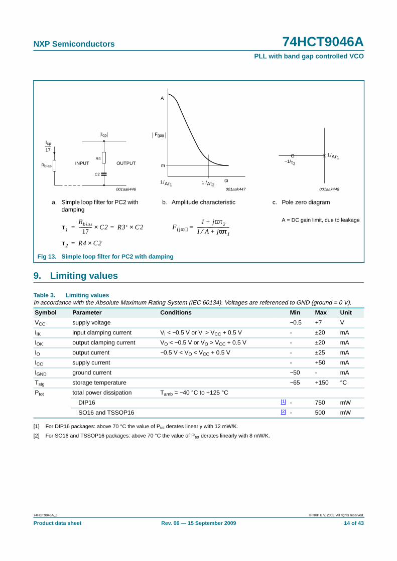
8.4 Loop filter component selectionExamples of PC2 combined with a passive filter are shown in Figure 12 and 13. Figure 12shows that PC2 with only a C2 filter behaves as a high-gain filter. For stability the dampedversion of Figure 13 with series resistance R4 is preferred.
Practical design values for Rbias are between 25 kΩ and 250 kΩ with R3' = 1.5 kΩto 15 kΩ for the filter design. Higher values for R3' require lower values for the filtercapacitance which is very advantageous at low values of the loop natural frequency ωn.
KPC25
4π------ V r⁄( )=
a. Simple loop filter for PC2without damping
b. Amplitude characteristic c. Pole zero diagram
A = DC gain limit, due to leakage
Fig 12. Simple loop filter for PC2 without damping
001aak449
OUTPUTINPUT C2
Icp
Icp
17
Rbias
001aak450
F(jω)
ω1/Aτ1
A
001aak451
−1/Aτ1
τ1
Rbias
17------------ C2× R3' C2×== F j ω( )
11 A⁄ jωτ1+-----------------------------
1jωτ1------------≈=
74HCT9046A_6 © NXP B.V. 2009. All rights reserved.
Product data sheet Rev. 06 — 15 September 2009 13 of 43
NXP Semiconductors 74HCT9046APLL with band gap controlled VCO
9. Limiting values
[1] For DIP16 packages: above 70 °C the value of Ptot derates linearly with 12 mW/K.
[2] For SO16 and TSSOP16 packages: above 70 °C the value of Ptot derates linearly with 8 mW/K.
a. Simple loop filter for PC2 withdamping
b. Amplitude characteristic c. Pole zero diagram
A = DC gain limit, due to leakage
Fig 13. Simple loop filter for PC2 with damping
001aak446
OUTPUTINPUTR4
C2
Icp
Icp
17
Rbias
001aak447
F(jω)
m
1 / ω1/Aτ1 Aτ2
A
001aak448
O−1/τ2
1/Aτ1
τ1
Rbias
17------------ C2× R3‘ C2×==
τ2 R4 C2×=
F j ω( )1 jωτ2+
1 A jωτ1+⁄-----------------------------=
Table 3. Limiting valuesIn accordance with the Absolute Maximum Rating System (IEC 60134). Voltages are referenced to GND (ground = 0 V).
Symbol Parameter Conditions Min Max Unit
VCC supply voltage −0.5 +7 V
IIK input clamping current VI < −0.5 V or VI > VCC + 0.5 V - ±20 mA
IOK output clamping current VO < −0.5 V or VO > VCC + 0.5 V - ±20 mA
IO output current −0.5 V < VO < VCC + 0.5 V - ±25 mA
ICC supply current - +50 mA
IGND ground current −50 - mA
Tstg storage temperature −65 +150 °C
Ptot total power dissipation Tamb = −40 °C to +125 °C
DIP16 [1] - 750 mW
SO16 and TSSOP16 [2] - 500 mW
74HCT9046A_6 © NXP B.V. 2009. All rights reserved.
Product data sheet Rev. 06 — 15 September 2009 14 of 43
NXP Semiconductors 74HCT9046APLL with band gap controlled VCO
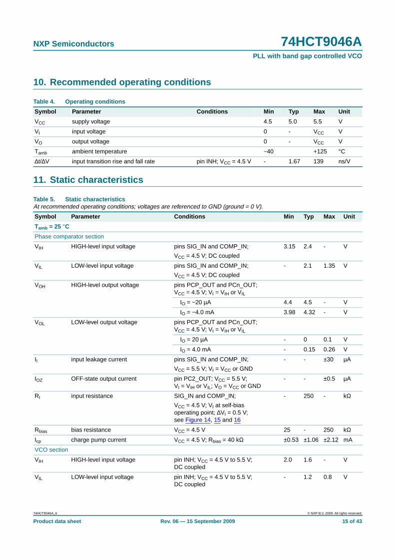
10. Recommended operating conditions
11. Static characteristics
Table 4. Operating conditions
Symbol Parameter Conditions Min Typ Max Unit
VCC supply voltage 4.5 5.0 5.5 V
VI input voltage 0 - VCC V
VO output voltage 0 - VCC V
Tamb ambient temperature −40 +125 °C
∆t/∆V input transition rise and fall rate pin INH; VCC = 4.5 V - 1.67 139 ns/V
Table 5. Static characteristicsAt recommended operating conditions; voltages are referenced to GND (ground = 0 V).
Symbol Parameter Conditions Min Typ Max Unit
Tamb = 25 °C
Phase comparator section
VIH HIGH-level input voltage pins SIG_IN and COMP_IN;
VCC = 4.5 V; DC coupled
3.15 2.4 - V
VIL LOW-level input voltage pins SIG_IN and COMP_IN;
VCC = 4.5 V; DC coupled
- 2.1 1.35 V
VOH HIGH-level output voltage pins PCP_OUT and PCn_OUT;VCC = 4.5 V; VI = VIH or VIL
IO = −20 µA 4.4 4.5 - V
IO = −4.0 mA 3.98 4.32 - V
VOL LOW-level output voltage pins PCP_OUT and PCn_OUT;VCC = 4.5 V; VI = VIH or VIL
IO = 20 µA - 0 0.1 V
IO = 4.0 mA - 0.15 0.26 V
II input leakage current pins SIG_IN and COMP_IN;
VCC = 5.5 V; VI = VCC or GND
- - ±30 µA
IOZ OFF-state output current pin PC2_OUT; VCC = 5.5 V;VI = VIH or VIL; VO = VCC or GND
- - ±0.5 µA
RI input resistance SIG_IN and COMP_IN;
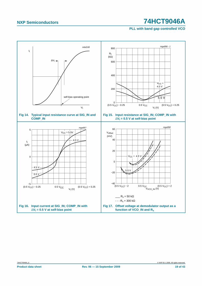
VCC = 4.5 V; VI at self-biasoperating point; ∆VI = 0.5 V;see Figure 14, 15 and 16
- 250 - kΩ
Rbias bias resistance VCC = 4.5 V 25 - 250 kΩ
Icp charge pump current VCC = 4.5 V; Rbias = 40 kΩ ±0.53 ±1.06 ±2.12 mA
VCO section
VIH HIGH-level input voltage pin INH; VCC = 4.5 V to 5.5 V;DC coupled
2.0 1.6 - V
VIL LOW-level input voltage pin INH; VCC = 4.5 V to 5.5 V;DC coupled
- 1.2 0.8 V
74HCT9046A_6 © NXP B.V. 2009. All rights reserved.
Product data sheet Rev. 06 — 15 September 2009 15 of 43

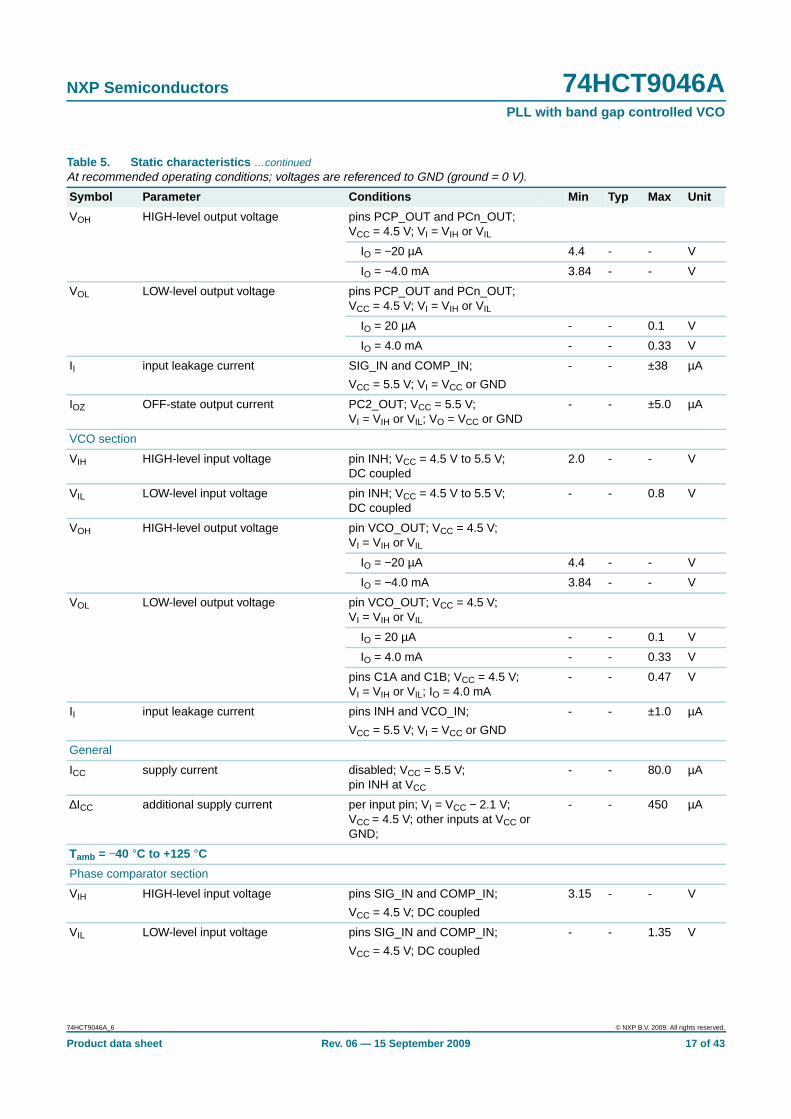
NXP Semiconductors 74HCT9046APLL with band gap controlled VCO
VOH HIGH-level output voltage pin VCO_OUT; VCC = 4.5 V;VI = VIH or VIL
IO = −20 µA 4.4 4.5 - V
IO = −4.0 mA 3.98 4.32 - V
VOL LOW-level output voltage pin VCO_OUT; VCC = 4.5 V;VI = VIH or VIL
IO = 20 µA - 0 0.1 V
IO = 4.0 mA - 0.15 0.26 V
pins C1A and C1B; VCC = 4.5 V;VI = VIH or VIL; IO = 4.0 mA
- - 0.40 V
II input leakage current pins INH and VCO_IN;VCC = 5.5 V; VI = VCC or GND
- - ±0.1 µA
R1 resistor 1 VCC = 4.5 V 3 - 300 kΩ
R2 resistor 2 VCC = 4.5 V 3 - 300 kΩ
C1 capacitor 1 VCC = 4.5 V 40 - nolimit
pF
VVCO_IN voltage on pin VCO_IN over the range specified for R1
VCC = 4.5 V 1.1 - 3.4 V
VCC = 5.0 V 1.1 - 3.9 V
VCC = 5.5 V 1.1 - 4.4 V
Demodulator section
Rs series resistance VCC = 4.5 V; at Rs > 300 kΩ theleakage current can influenceVDEM_OUT
50 - 300 kΩ
Voffset offset voltage VCO_IN to VDEM_OUT; VCC = 4.5 V;VI = VVCO_IN = 0.5VCC; valuestaken over Rs range; see Figure 17
- ±20 - mV
Rdyn dynamic resistance DEM_OUT; VCC = 4.5 V;VDEM_OUT = 0.5VCC
- 25 - Ω
General
ICC supply current disabled; VCC = 5.5 V;pin INH at VCC
- - 8.0 µA
∆ICC additional supply current pin INH; VI = VCC − 2.1 V; VCC =4.5 V; other inputs at VCC or GND;
- 100 360 µA
CI input capacitance - 3.5 - pF
Tamb = −40 °C to +85 °C
Phase comparator section
VIH HIGH-level input voltage pins SIG_IN and COMP_IN;
VCC = 4.5 V; DC coupled
3.15 - - V
VIL LOW-level input voltage pins SIG_IN and COMP_IN;
VCC = 4.5 V; DC coupled
- - 1.35 V
Table 5. Static characteristics …continuedAt recommended operating conditions; voltages are referenced to GND (ground = 0 V).
Symbol Parameter Conditions Min Typ Max Unit
74HCT9046A_6 © NXP B.V. 2009. All rights reserved.
Product data sheet Rev. 06 — 15 September 2009 16 of 43
NXP Semiconductors 74HCT9046APLL with band gap controlled VCO
VOH HIGH-level output voltage pins PCP_OUT and PCn_OUT;VCC = 4.5 V; VI = VIH or VIL
IO = −20 µA 4.4 - - V
IO = −4.0 mA 3.84 - - V
VOL LOW-level output voltage pins PCP_OUT and PCn_OUT;VCC = 4.5 V; VI = VIH or VIL
IO = 20 µA - - 0.1 V
IO = 4.0 mA - - 0.33 V
II input leakage current SIG_IN and COMP_IN;
VCC = 5.5 V; VI = VCC or GND
- - ±38 µA
IOZ OFF-state output current PC2_OUT; VCC = 5.5 V;VI = VIH or VIL; VO = VCC or GND
- - ±5.0 µA
VCO section
VIH HIGH-level input voltage pin INH; VCC = 4.5 V to 5.5 V;DC coupled
2.0 - - V
VIL LOW-level input voltage pin INH; VCC = 4.5 V to 5.5 V;DC coupled
- - 0.8 V
VOH HIGH-level output voltage pin VCO_OUT; VCC = 4.5 V;VI = VIH or VIL
IO = −20 µA 4.4 - - V
IO = −4.0 mA 3.84 - - V
VOL LOW-level output voltage pin VCO_OUT; VCC = 4.5 V;VI = VIH or VIL
IO = 20 µA - - 0.1 V
IO = 4.0 mA - - 0.33 V
pins C1A and C1B; VCC = 4.5 V;VI = VIH or VIL; IO = 4.0 mA
- - 0.47 V
II input leakage current pins INH and VCO_IN;
VCC = 5.5 V; VI = VCC or GND
- - ±1.0 µA
General
ICC supply current disabled; VCC = 5.5 V;pin INH at VCC
- - 80.0 µA
∆ICC additional supply current per input pin; VI = VCC − 2.1 V;VCC = 4.5 V; other inputs at VCC orGND;
- - 450 µA
Tamb = −40 °C to +125 °C
Phase comparator section
VIH HIGH-level input voltage pins SIG_IN and COMP_IN;
VCC = 4.5 V; DC coupled
3.15 - - V
VIL LOW-level input voltage pins SIG_IN and COMP_IN;
VCC = 4.5 V; DC coupled
- - 1.35 V
Table 5. Static characteristics …continuedAt recommended operating conditions; voltages are referenced to GND (ground = 0 V).
Symbol Parameter Conditions Min Typ Max Unit
74HCT9046A_6 © NXP B.V. 2009. All rights reserved.
Product data sheet Rev. 06 — 15 September 2009 17 of 43

NXP Semiconductors 74HCT9046APLL with band gap controlled VCO
VOH HIGH-level output voltage pins PCP_OUT and PCn_OUT;
VCC = 4.5 V; VI = VIH or VIL
IO = −20 µA 4.4 - - V
IO = −4.0 mA 3.7 - - V
VOL LOW-level output voltage pins PCP_OUT and PCn_OUT;
VCC = 4.5 V; VI = VIH or VIL
IO = 20 µA - - 0.1 V
IO = 4.0 mA - - 0.4 V
II input leakage current pins SIG_IN and COMP_IN;
VCC = 5.5 V; VI = VCC or GND
- - ±45 µA
IOZ OFF-state output current pin PC2_OUT; VCC = 5.5 V;VI = VIH or VIL; VO = VCC or GND
- - ±10.0 µA
VCO section
VIH HIGH-level input voltage pin INH; VCC = 4.5 V to 5.5 V;DC coupled
2.0 - - V
VIL LOW-level input voltage pin INH; VCC = 4.5 V to 5.5 V;DC coupled
- - 0.8 V
VOH HIGH-level output voltage pin VCO_OUT; VCC = 4.5 V;VI = VIH or VIL
IO = −20 µA 4.4 - - V
IO = −4.0 mA 3.7 - - V
VOL LOW-level output voltage pin VCO_OUT; VCC = 4.5 V;VI = VIH or VIL
IO = 20 µA - - 0.1 V
IO = 4.0 mA - - 0.4 V
pins C1A and C1B; VCC = 4.5 V;VI = VIH or VIL; IO = 4.0 mA
- - 0.54 V
II input leakage current pins INH and VCO_IN;
VCC = 5.5 V; VCC or GND
- - ±1.0 µA
General
ICC supply current disabled; VCC = 5.5 V;pin INH at VCC
- - 160.0 µA
∆ICC additional supply current per input pin; VI = VCC − 2.1 V;VCC = 4.5 V; other inputs at VCC orGND;
- - 490 µA
Table 5. Static characteristics …continuedAt recommended operating conditions; voltages are referenced to GND (ground = 0 V).
Symbol Parameter Conditions Min Typ Max Unit
74HCT9046A_6 © NXP B.V. 2009. All rights reserved.
Product data sheet Rev. 06 — 15 September 2009 18 of 43
NXP Semiconductors 74HCT9046APLL with band gap controlled VCO
Fig 14. Typical input resistance curve at SIG_IN andCOMP_IN
Fig 15. Input resistance at SIG_IN; COMP_IN with∆VI = 0.5 V at self-bias point
___ Rs = 50 kΩ- - - Rs = 300 kΩ
Fig 16. Input current at SIG_IN; COMP_IN with∆VI = 0.5 V at self-bias point
Fig 17. Offset voltage at demodulator output as afunction of VCO_IN and R s
mbd108
self-bias operating point
VI
∆VI
II800
600
200
0
400
mga956 - 1
VI (V)(0.5 VCC) − 0.25 0.5 VCC (0.5 VCC) + 0.25
RI(kΩ)
5.5 V
VCC =4.5 V
5
−5
0
mga957
VI (V)(0.5 VCC) − 0.25 0.5 VCC (0.5 VCC) + 0.25
II(µA)
4.5 V
VCC = 5.5V
5.5 V
4.5 V
40
−40
0
mga958
(0.5 VCC) − 2 (0.5 VCC) + 20.5 VCC
−20
20
60Voffset
(mV)
VVCO_IN (V)
5.5 V
4.5 VVCC =
74HCT9046A_6 © NXP B.V. 2009. All rights reserved.
Product data sheet Rev. 06 — 15 September 2009 19 of 43
NXP Semiconductors 74HCT9046APLL with band gap controlled VCO
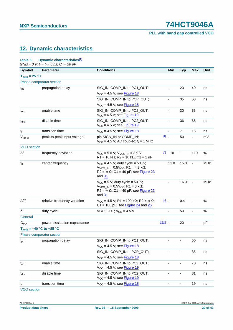
12. Dynamic characteristics
Table 6. Dynamic characteristics [1]
GND = 0 V; tr = tf = 6 ns; CL = 50 pF.
Symbol Parameter Conditions Min Typ Max Unit
Tamb = 25 °C
Phase comparator section
tpd propagation delay SIG_IN, COMP_IN to PC1_OUT;
VCC = 4.5 V; see Figure 18
- 23 40 ns
SIG_IN, COMP_IN to PCP_OUT;
VCC = 4.5 V; see Figure 18
- 35 68 ns
ten enable time SIG_IN, COMP_IN to PC2_OUT;VCC = 4.5 V; see Figure 19
- 30 56 ns
tdis disable time SIG_IN, COMP_IN to PC2_OUT;VCC = 4.5 V; see Figure 19
- 36 65 ns
tt transition time VCC = 4.5 V; see Figure 18 - 7 15 ns
Vi(p-p) peak-to-peak input voltage pin SIGN_IN or COMP_IN;VCC = 4.5 V; AC coupled; fi = 1 MHz
[4] - 50 - mV
VCO section
∆f frequency deviation VCC = 5.0 V; VVCO_IN = 3.9 V;R1 = 10 kΩ; R2 = 10 kΩ; C1 = 1 nF
[5] −10 - +10 %
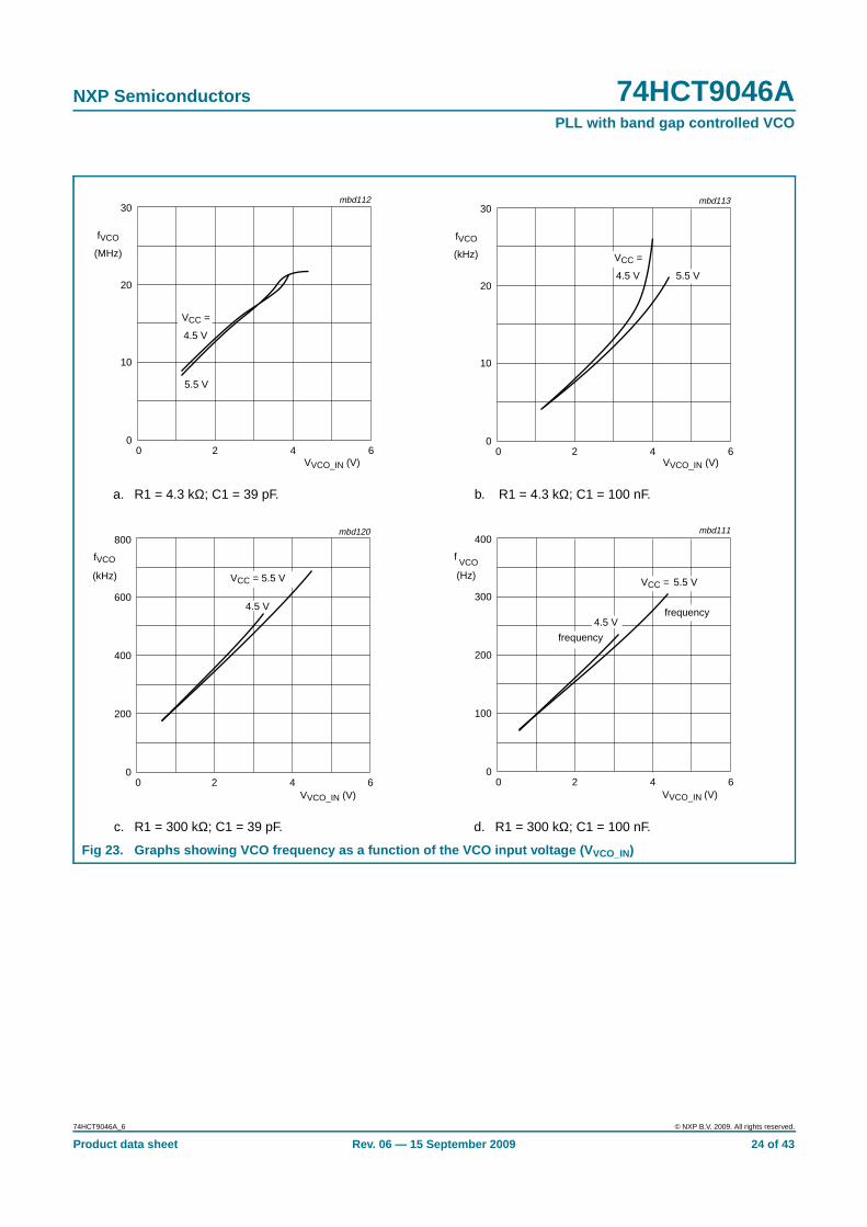
f0 center frequency VCC = 4.5 V; duty cycle = 50 %;VVCO_IN = 0.5VCC; R1 = 4.3 kΩ;R2 = ∞ Ω; C1 = 40 pF; see Figure 23and 31
11.0 15.0 - MHz
VCC = 5 V; duty cycle = 50 %;VVCO_IN = 0.5VCC; R1 = 3 kΩ;R2 = ∞ Ω; C1 = 40 pF; see Figure 23and 31
- 16.0 - MHz
∆f/f relative frequency variation VCC = 4.5 V; R1 = 100 kΩ; R2 = ∞ Ω;C1 = 100 pF; see Figure 24 and 25
[6] - 0.4 - %
δ duty cycle VCO_OUT; VCC = 4.5 V - 50 - %
General
CPD power dissipation capacitance [2][3] - 20 - pF
Tamb = −40 °C to +85 °C
Phase comparator section
tpd propagation delay SIG_IN, COMP_IN to PC1_OUT;
VCC = 4.5 V; see Figure 18
- - 50 ns
SIG_IN, COMP_IN to PCP_OUT;
VCC = 4.5 V; see Figure 18
- - 85 ns
ten enable time SIG_IN, COMP_IN to PC2_OUT;VCC = 4.5 V; see Figure 19
- - 70 ns
tdis disable time SIG_IN, COMP_IN to PC2_OUT;VCC = 4.5 V; see Figure 19
- - 81 ns
tt transition time VCC = 4.5 V; see Figure 18 - - 19 ns
VCO section
74HCT9046A_6 © NXP B.V. 2009. All rights reserved.
Product data sheet Rev. 06 — 15 September 2009 20 of 43

NXP Semiconductors 74HCT9046APLL with band gap controlled VCO
[1] tpd is the same as tPLH and tPHL; tdis is the same as tPLZ and tPHZ; ten is the same as tPZL and tPZH; tt is the same as tTLH and tTHL.
[2] CPD is used to determine the dynamic power dissipation (PD in µW).
PD = CPD × VCC2 × fi × N + ∑(CL × VCC
2 × fo) where:
fi = input frequency in MHz;
fo = output frequency in MHz;
CL = output load capacitance in pF;
VCC = supply voltage in V;
N = total load switching outputs;
∑(CL × VCC2 × fo) = sum of outputs.
[3] Applies to the phase comparator section only (pin INH = HIGH). For power dissipation of the VCO and demodulator sections, seeFigure 26, 27 and 28.
[4] This is the (peak to peak) input sensitivity.
[5] This is the center frequency tolerance.
[6] This is the frequency linearity.
[7] This is the frequency stability with temperature change.
∆f/∆T frequency variation withtemperature
VCC = 4.5 V; VVCO_IN = 0.5VCC;recommended range: R1 = 10 kΩ;R2 = 10 kΩ; C1 = 1 nF; see Figure 20,21 and 22
[7] - 0.06 - %/K
Tamb = −40 °C to +125 °C
Phase comparator section
tpd propagation delay SIG_IN, COMP_IN to PC1_OUT;
VCC = 4.5 V; see Figure 18
- - 60 ns
SIG_IN, COMP_IN to PCP_OUT;
VCC = 4.5 V; see Figure 18
- - 102 ns
ten enable time SIG_IN, COMP_IN to PC2_OUT;VCC = 4.5 V; see Figure 19
- - 84 ns
tdis disable time SIG_IN, COMP_IN to PC2_OUT;
VCC = 4.5 V; see Figure 19
- - 98 ns
tt transition time VCC = 4.5 V; see Figure 18 - - 22 ns
Table 6. Dynamic characteristics [1] …continuedGND = 0 V; tr = tf = 6 ns; CL = 50 pF.
Symbol Parameter Conditions Min Typ Max Unit
VM = 0.5VCC; VI = GND to VCC.
Fig 18. Waveforms showing input (SIG_IN and COMP_IN) to output (PCP_OUT and PC1_OUT) propagationdelays and the output transition times
mbd106
tPHL
tTHL
tPLH
tTLH
SIG_IN, COMP_INinputs
PCP_OUT, PC1_OUToutputs
VM
VM
74HCT9046A_6 © NXP B.V. 2009. All rights reserved.
Product data sheet Rev. 06 — 15 September 2009 21 of 43

NXP Semiconductors 74HCT9046APLL with band gap controlled VCO
VM = 0.5VCC; VI = GND to VCC.
Fig 19. Waveforms showing the enable and disable times for PC2_OUT
mga941
tPLZtPZH
tPHZ
10%
90%
tPZL
SIG_INinput
COMP_INinput
PC2_OUToutput
VM
VM
VM
a. R1 = 3 kΩ; R2 = ∞ Ω; C1 = 100 pF. b. R1 = 10 kΩ; R2 = ∞ Ω; C1 = 100 pF.
Fig 20. Frequency stability of the VCO as a function of ambient temperature with supply voltage as a parameter
−50 0 50 150
20
10
−10
−20
0
mbd115
100
∆ f(%)
5.5 V
4.5 V
VCC =
Tamb (°C)
mbd116
Tamb (°C)
0
f(%)
150100500−50−15
−10
−5
5
10
15∆
5.5 V
4.5 V
VCC =
74HCT9046A_6 © NXP B.V. 2009. All rights reserved.
Product data sheet Rev. 06 — 15 September 2009 22 of 43

NXP Semiconductors 74HCT9046APLL with band gap controlled VCO
a. R1 = 300 kΩ; R2 = ∞ Ω; C1 = 100 pF. b. R1 = ∞ Ω; R2 = 3 kΩ; C1 = 100 pF.
Fig 21. Frequency stability of the VCO as a function of ambient temperature with supply voltage as a parameter
−50 0 50 150
10
5
−5
−10
0
mbd124
100
∆ f(%)
5.5 V
4.5 V
VCC =
Tamb (°C)
mbd117
Tamb (°C)
0
f(%)
150100500−50−20
−15
−10
5
10
15∆
5.5 V
4.5 V
VCC =
−5
a. R1 = ∞ Ω; R2 = 10 kΩ; C1 = 100 pF. b. R1 = ∞ Ω; R2 = 300 kΩ; C1 = 100 pF.
Fig 22. Frequency stability of the VCO as a function of ambient temperature with supply voltage as a parameter
mbd118
Tamb (°C)
0
f(%)
150100500−50−12
−8
−4
4
8
∆
5.5 V
4.5 V
VCC =
mbd119
Tamb (°C)
0
f(%)
150100500−50−10
−5
5
10
∆
5.5 V
4.5 V
VCC =
74HCT9046A_6 © NXP B.V. 2009. All rights reserved.
Product data sheet Rev. 06 — 15 September 2009 23 of 43
NXP Semiconductors 74HCT9046APLL with band gap controlled VCO
a. R1 = 4.3 kΩ; C1 = 39 pF. b. R1 = 4.3 kΩ; C1 = 100 nF.
c. R1 = 300 kΩ; C1 = 39 pF. d. R1 = 300 kΩ; C1 = 100 nF.
Fig 23. Graphs showing VCO frequency as a function of the VCO input voltage (V VCO_IN)
0 2 4 6
30
10
0
20
mbd112
VVCO_IN (V)
fVCO
(MHz)
5.5 V
4.5 V
VCC =
0 2 4 6
30
10
0
20
mbd113
fVCO
(kHz)
5.5 V4.5 V
VCC =
VVCO_IN (V)
0 2 4 6
800
600
200
0
400
mbd120
fVCO
(kHz)
VVCO_IN (V)
VCC = 5.5 V
4.5 V
0 2 4 6
400
300
100
0
200
mbd111
fVCO
(Hz)
frequency
frequency4.5 V
5.5 VVCC =
VVCO_IN (V)
74HCT9046A_6 © NXP B.V. 2009. All rights reserved.
Product data sheet Rev. 06 — 15 September 2009 24 of 43

NXP Semiconductors 74HCT9046APLL with band gap controlled VCO
linearity =
R2 = ∞ Ω and ∆V = 0.5 V
Fig 24. Definition of VCO frequency linearity:∆V = 0.5 V over the V CC range
Fig 25. Frequency linearity as a function of R1, C1 andVCC
R2 = ∞ Ω R1 = ∞ Ω
Fig 26. Power dissipation as a function of R1 Fig 27. Power dissipation as a function of R2
mga937
f(MHz)
max
f1
min 0.5 VCC
f'0
f 0
f2
VVCO_IN (V)
V V
4
−4
0
1
mbd114
10 102 103−8
fVCO
(%)
R1 (kΩ)
C1 = 1 µF4.5 V5.5 V
C1 = 39 pF
4.5 V
5.5 V
f‘ 0
f 1 f 2+
2------------------=
f‘ 0 f 0–
f 0------------------ 100 %×
3000 100
mbd121
10 1
1
20010 2
R1 (kΩ)
4.5 VC1 = 1 µF
5.5 VC1 = 39 pF
4.5 VC1 = 39 pF
5.5 VC1 = 1 µF
VCC =PD
(W)
3000 100
mbd110
10 1
1
20010 2
R2 (kΩ)
PD 5.5 VC1 = 39 pF
5.5 V4.5 VC1 = 1 µF
4.5 VC1 = 39 pF
VCC =
(W)
74HCT9046A_6 © NXP B.V. 2009. All rights reserved.
Product data sheet Rev. 06 — 15 September 2009 25 of 43

NXP Semiconductors 74HCT9046APLL with band gap controlled VCO
Fig 28. Typical power dissipation as a function of R s
103
mbd109
10210
10 4
PDEM(W)
Rs (kΩ)10 5
10 3
VCC =
5.5 V4.5 V
74HCT9046A_6 © NXP B.V. 2009. All rights reserved.
Product data sheet Rev. 06 — 15 September 2009 26 of 43
NXP Semiconductors 74HCT9046APLL with band gap controlled VCO
13. Application information
This information is a guide for the approximation of values of external components to beused with the 74HCT9046A in a phase-locked-loop system.
Values of the selected components should be within the ranges shown in Table 7.
Table 7. Survey of components
Component Value
R1 between 3 kΩ and 300 kΩ
R2 between 3 kΩ and 300 kΩ
R1 + R2 parallel value > 2.7 kΩ
C1 > 40 pF
Table 8. Design considerations for VCO section
Subject Phase comparator Design consideration
VCO frequencywithout extraoffset
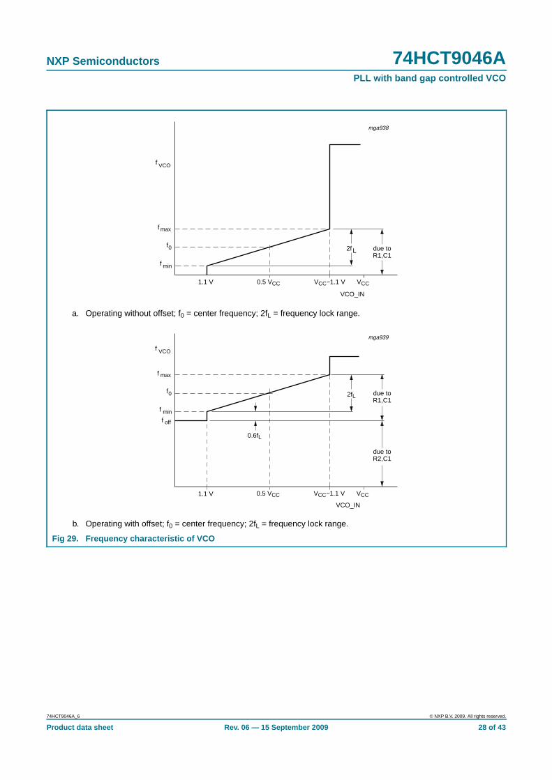
PC1, PC2 VCO frequency characteristic. With R2 = ∞ and R1 within the range3 kΩ < R1 < 300 kΩ, the characteristics of the VCO operation will be asshown in Figure 29a. (Due to R1, C1 time constant a small offset remainswhen R2 = ∞ Ω).
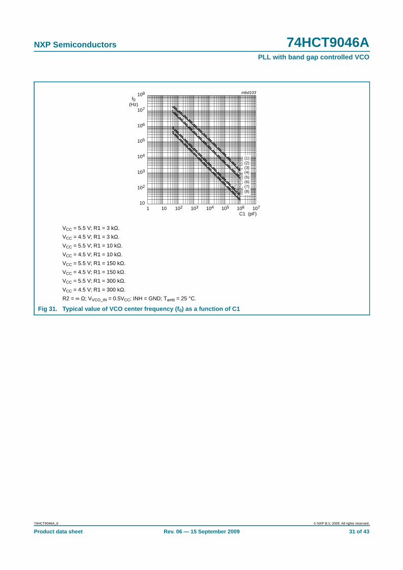
PC1 Selection of R1 and C1. Given f0, determine the values of R1 and C1 usingFigure 31.
PC2 Given fmax and f0 determine the values of R1 and C1 using Figure 31; useFigure 33 to obtain 2fL and then use this to calculate fmin.
VCO frequencywith extra offset
PC1, PC2 VCO frequency characteristic. With R1 and R2 within the ranges3 kΩ < R1 < 300 kΩ < R2 < 300 kΩ, the characteristics of the VCOoperation is as shown in Figure 29b.
PC1, PC2 Selection of R1, R2 and C1. Given f0 and fL determine the value of productR1C1 by using Figure 33. Calculate foff from the equation foff = f0 − 1.6fL.Obtain the values of C1 and R2 by using Figure 32. Calculate the value ofR1 from the value of C1 and the product R1C1.
PLL conditions withno signal at pinSIG_IN
PC1 VCO adjusts to f0 with ΦPC_IN = 90° and VVCO_IN = 0.5VCC
PC2 VCO adjusts to foffset with ΦPC_IN = −360° and VVCO_IN = minimum
74HCT9046A_6 © NXP B.V. 2009. All rights reserved.
Product data sheet Rev. 06 — 15 September 2009 27 of 43
NXP Semiconductors 74HCT9046APLL with band gap controlled VCO
a. Operating without offset; f0 = center frequency; 2fL = frequency lock range.
b. Operating with offset; f0 = center frequency; 2fL = frequency lock range.
Fig 29. Frequency characteristic of VCO
mga938
f VCO
f max
f0
f min
1.1 V 0.5 VCC VCCVCC−1.1 V
VCO_IN
2fL due toR1,C1
0.6fL
f off
f VCO
f max
f0
f min
1.1 V
VCO_IN
2fL due toR1,C1
due toR2,C1
mga939
0.5 VCC VCCVCC−1.1 V
74HCT9046A_6 © NXP B.V. 2009. All rights reserved.
Product data sheet Rev. 06 — 15 September 2009 28 of 43
NXP Semiconductors 74HCT9046APLL with band gap controlled VCO
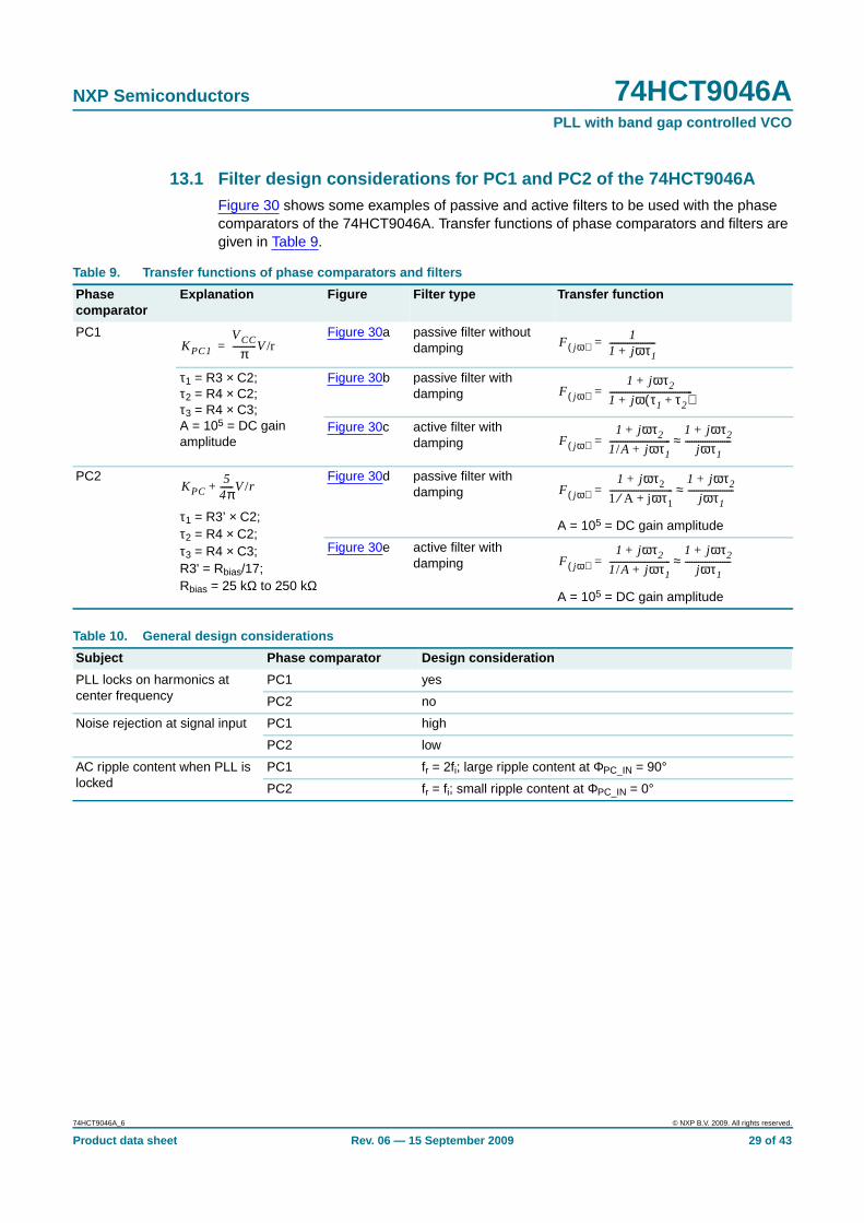
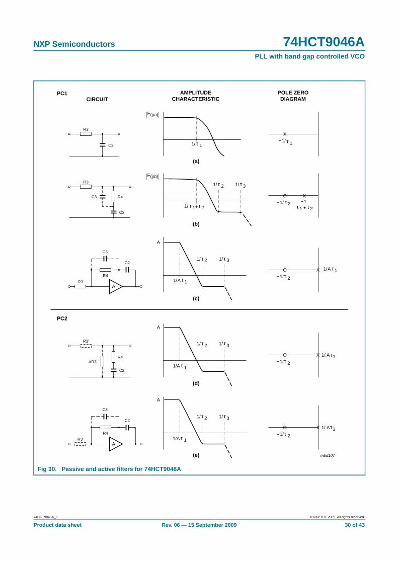
13.1 Filter design considerations for PC1 and PC2 of the 74HCT9046AFigure 30 shows some examples of passive and active filters to be used with the phasecomparators of the 74HCT9046A. Transfer functions of phase comparators and filters aregiven in Table 9.
Table 9. Transfer functions of phase comparators and filters
Phasecomparator
Explanation Figure Filter type Transfer function
PC1 Figure 30a passive filter withoutdamping
τ1 = R3 × C2;τ2 = R4 × C2;τ3 = R4 × C3;A = 105 = DC gainamplitude
Figure 30b passive filter withdamping
Figure 30c active filter withdamping
PC2
τ1 = R3’ × C2;τ2 = R4 × C2;τ3 = R4 × C3;R3' = Rbias/17;Rbias = 25 kΩ to 250 kΩ
Figure 30d passive filter withdamping
A = 105 = DC gain amplitude
Figure 30e active filter withdamping
A = 105 = DC gain amplitude
KPC1
VCC
π-----------V/r= F j ω( )1
1 jωτ1+---------------------=
F j ω( )1 jωτ2+
1 jω τ1 τ2+( )+--------------------------------------=
F j ω( )1 jωτ2+
1/A jωτ1+----------------------------
1 jωτ2+
jωτ1---------------------≈=
KPC5
4π------V/r+ F j ω( )1 jωτ2+
1 A⁄ jωτ1+-----------------------------
1 jωτ2+
jωτ1---------------------≈=
F j ω( )1 jωτ2+
1/A jωτ1+----------------------------
1 jωτ2+
jωτ1---------------------≈=
Table 10. General design considerations
Subject Phase comparator Design consideration
PLL locks on harmonics atcenter frequency
PC1 yes
PC2 no
Noise rejection at signal input PC1 high
PC2 low
AC ripple content when PLL islocked
PC1 fr = 2fi; large ripple content at ΦPC_IN = 90°
PC2 fr = fi; small ripple content at ΦPC_IN = 0°
74HCT9046A_6 © NXP B.V. 2009. All rights reserved.
Product data sheet Rev. 06 — 15 September 2009 29 of 43
NXP Semiconductors 74HCT9046APLL with band gap controlled VCO
Fig 30. Passive and active filters for 74HCT9046A
mbd107
X1/ τ
R3
C2
F(jω)
R3
C2
C3 R4
C3
A
R4
C2
R3
R3'
C2
R4AR3'
A
C3
R4
C2
Oτ
X
2 1τ1 τ2
Oτ
X
2
1/ τ 2 1/ τ3
1/
Oτ
X
2
1/ Aτ1/
1
Oτ
X
2
1/ Aτ1/
1
A
1/ τ2 1/ τ3
1/ τ1A
A
1/ τ2 1/ τ3
τ 11/A
A
1/ τ2 1/ τ3
CIRCUITAMPLITUDE
CHARACTERISTICPOLE ZERODIAGRAM
1/ τ 1 1
τ1 τ21/
1/ τ1A
PC2
PC1
(a)
(b)
(c)
(d)
(e)
τ 11/AR3'
1/
F(jω)
74HCT9046A_6 © NXP B.V. 2009. All rights reserved.
Product data sheet Rev. 06 — 15 September 2009 30 of 43
NXP Semiconductors 74HCT9046APLL with band gap controlled VCO
VCC = 5.5 V; R1 = 3 kΩ.
VCC = 4.5 V; R1 = 3 kΩ.
VCC = 5.5 V; R1 = 10 kΩ.
VCC = 4.5 V; R1 = 10 kΩ.
VCC = 5.5 V; R1 = 150 kΩ.
VCC = 4.5 V; R1 = 150 kΩ.
VCC = 5.5 V; R1 = 300 kΩ.
VCC = 4.5 V; R1 = 300 kΩ.
R2 = ∞ Ω; VVCO_IN = 0.5VCC; INH = GND; Tamb = 25 °C.
Fig 31. Typical value of VCO center frequency (f 0) as a function of C1
mbd103
107105104103101
105
103
10
102
104
106
106
C1 (pF)
107
108
102
f0(Hz)
(1)(2)(3)(4)(5)(6)(7)(8)
74HCT9046A_6 © NXP B.V. 2009. All rights reserved.
Product data sheet Rev. 06 — 15 September 2009 31 of 43
NXP Semiconductors 74HCT9046APLL with band gap controlled VCO
VCC = 4.5 V to 5.5 V; R1 = 3 kΩ.
VCC = 4.5 V to 5.5 V; R1 = 10 kΩ.
VCC = 4.5 V to 5.5 V; R1 = 150 kΩ.
VCC = 4.5 V to 5.5 V; R1 = 300 kΩ.
R1 = ∞ Ω; VVCO_IN = 0.5VCC; INH = GND; Tamb = 25 °C.
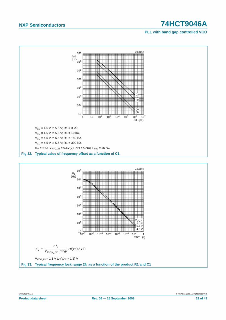
Fig 32. Typical value of frequency offset as a function of C1
mbd104
107105104103101
105
103
10
102
104
106
106
C1 (pF)
107
108
102
foff(Hz)
(2)
(1)
(3)(4)
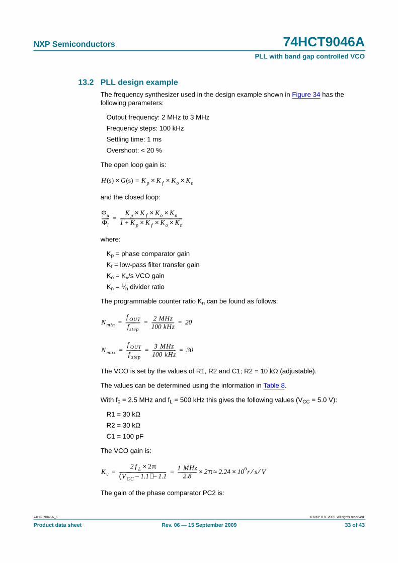
VVCO_IN = 1.1 V to (VCC − 1.1) V
Fig 33. Typical frequency lock range 2f L as a function of the product R1 and C1
mbd105
10−7
105
103
10
102
104
106
R1C1 (s)
107
108
2fL(Hz)
VCC =
10−6 10−5 10−4 10−3 10−2 10−1 1
5.5 V4.5 V
Kv
2 f L
VVCO_IN range----------------------------------------2π r s V⁄⁄( )=
74HCT9046A_6 © NXP B.V. 2009. All rights reserved.
Product data sheet Rev. 06 — 15 September 2009 32 of 43
NXP Semiconductors 74HCT9046APLL with band gap controlled VCO
13.2 PLL design exampleThe frequency synthesizer used in the design example shown in Figure 34 has thefollowing parameters:
Output frequency: 2 MHz to 3 MHz
Frequency steps: 100 kHz
Settling time: 1 ms
Overshoot: < 20 %
The open loop gain is:
and the closed loop:
where:
Kp = phase comparator gain
Kf = low-pass filter transfer gain
Ko = Kv/s VCO gain
Kn = 1⁄n divider ratio
The programmable counter ratio Kn can be found as follows:
The VCO is set by the values of R1, R2 and C1; R2 = 10 kΩ (adjustable).
The values can be determined using the information in Table 8.
With f0 = 2.5 MHz and fL = 500 kHz this gives the following values (VCC = 5.0 V):
R1 = 30 kΩ
R2 = 30 kΩ
C1 = 100 pF
The VCO gain is:
The gain of the phase comparator PC2 is:
H (s) G(s) K p K f Ko Kn×××=×
Φu
Φi-------
K p K f Ko Kn×××1 Kp K f Ko Kn×××+--------------------------------------------------------=
Nmin
f OUT
fstep-------------
2 MHz100 kHz-------------------- 20= = =
Nmax
f OUT
f step-------------
3 MHz100 kHz--------------------- 30= = =
Kv
2 f L 2π×VCC 1.1–( ) 1.1–
------------------------------------------1 MHz
2.8----------------- 2π 2.24 10
6r s V⁄⁄×≈×= =
74HCT9046A_6 © NXP B.V. 2009. All rights reserved.
Product data sheet Rev. 06 — 15 September 2009 33 of 43
NXP Semiconductors 74HCT9046APLL with band gap controlled VCO
Using PC2 with the passive filter as shown in Figure 34 results in a high gain loop with thesame performance as a loop with an active filter. Hence loop filter equations as for a highgain loop should be used. The current source output of PC2 can be simulated then with afictive filter resistance:
The transfer functions of the filter is given by:
Where:
The characteristic equation is:
This results in:
or:
This can be written as:
with the natural frequency ωn defined as:
and the damping value given as:
In Figure 35 the output frequency response to a step of input frequency is shown.
The overshoot and settling time percentages are now used to determine ωn.From Figure 35 it can be seen that the damping ratio ζ = 0.707 will produce an overshootof less than 20 % and settle to within 5 % at ωnt = 5. The required settling time is 1 ms.This results in:
K p5
4 π×------------ 0.4 V r⁄= =
R3‘Rbias
17------------=
K f
1 sτ2+
sτ2-----------------=
τ1 R3‘ C2×=
τ2 R4 C2×=
1 Kp K f Ko Kn×××+
1 Kp
1 sτ2+
sτ1-----------------
+Kv
s------Kn 0=
s2
sKpKvKn
τ2
τ1----- K pKvKn τ⁄ 1 0=++
s2
2ξωns ωn( )20=+ +
ωn
K p Kv Kn××τ1
---------------------------------=
ζ 0.5 τ2 ωn××=
74HCT9046A_6 © NXP B.V. 2009. All rights reserved.
Product data sheet Rev. 06 — 15 September 2009 34 of 43

NXP Semiconductors 74HCT9046APLL with band gap controlled VCO
Rewriting the equation for natural frequency results in:
The maximum overshoot occurs at Nmax = 30; hence Kn = 1⁄30:
When C2 = 470 nF, it follows:
Hence the current source bias resistance
With ζ = 0.707 (0.5 × τ2 × ωn) it follows:
For extra ripple suppression a capacitor C3 can be connected in parallel with R4, with anextra τ3 = R4 × C3.
For stability reasons τ3 should be < 0.1τ2, hence C3 < 0.1C2 or C3 = 39 nF.
ωn5t---
50.001------------- 5 10
3r s⁄×= = =
τ1
K p Kv Kn××
ωn( )2---------------------------------=
τ10.4 2.24 10
6××5000
230×
--------------------------------------- 0.0012= =
R3‘τ1
C2-------
0.0012
470 109–×
-------------------------- 2550 Ω= = =
Rbias 17 2550 43kΩ=×=
τ20.707
0.5 5000×------------------------- 0.00028= =
R4τ2
C2-------
0.00028
470 109–×
-------------------------- 600 Ω= = =
74HCT9046A_6 © NXP B.V. 2009. All rights reserved.
Product data sheet Rev. 06 — 15 September 2009 35 of 43

NXP Semiconductors 74HCT9046APLL with band gap controlled VCO
(1) R3’ = fictive resistance
R3’ =
C1 = 100 pF
C2 = 470 nF
C3 = 39 nF
R1 = 30 kΩR2 = 30 kΩR3' = 2550 ΩRbias = 43 kΩR4 = 600 Ω
Fig 34. Frequency synthesizer
mbd098
R4
C2R2R1
VCOR3'PHASE
COMPARATORPC2
DIVIDE BY 10"190"
OSCILLATOR"HCU04"
13100 kHz
14
3
4fOUT
PROGRAMMABLEDIVIDER
"4059"
9
11 12 6 7 5
1 MHz
Kp
Kn
Kf Ko
C1
C3
(1)
Rbias
15
Φu
Rbias
17------------
Fig 35. Type 2, second order frequency step response
0 1 2 4
1.6
1.0
0.6
0
0.8
mga959
3
1.4
1.2
0.4
0.2
5 6 7 8ωnt
∆Φe(t)
∆Φe/ωn
∆ωe(t)
∆ωe/ωn
−0.6
0
0.4
1.0
0.2
−0.4
−0.2
0.6
0.8
= 5.0ζ
0.50.7071.0
= 0.3ζ
= 2.0ζ
74HCT9046A_6 © NXP B.V. 2009. All rights reserved.
Product data sheet Rev. 06 — 15 September 2009 36 of 43
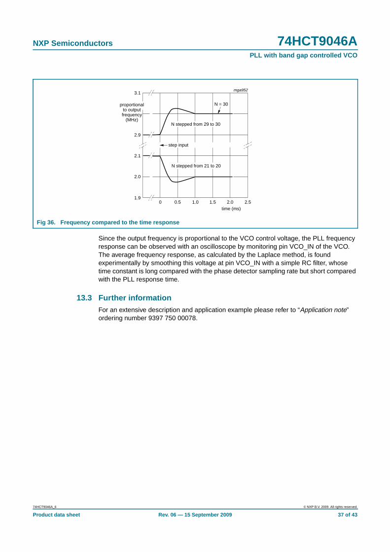
NXP Semiconductors 74HCT9046APLL with band gap controlled VCO
Since the output frequency is proportional to the VCO control voltage, the PLL frequencyresponse can be observed with an oscilloscope by monitoring pin VCO_IN of the VCO.The average frequency response, as calculated by the Laplace method, is foundexperimentally by smoothing this voltage at pin VCO_IN with a simple RC filter, whosetime constant is long compared with the phase detector sampling rate but short comparedwith the PLL response time.
13.3 Further informationFor an extensive description and application example please refer to “Application note”ordering number 9397 750 00078.
Fig 36. Frequency compared to the time response
mga9523.1
2.9
2.1
2.0
1.90 0.5 1.0 1.5 2.0 2.5
time (ms)
proportionalto outputfrequency
(MHz)
N = 30
N stepped from 29 to 30
step input
N stepped from 21 to 20
74HCT9046A_6 © NXP B.V. 2009. All rights reserved.
Product data sheet Rev. 06 — 15 September 2009 37 of 43
NXP Semiconductors 74HCT9046APLL with band gap controlled VCO
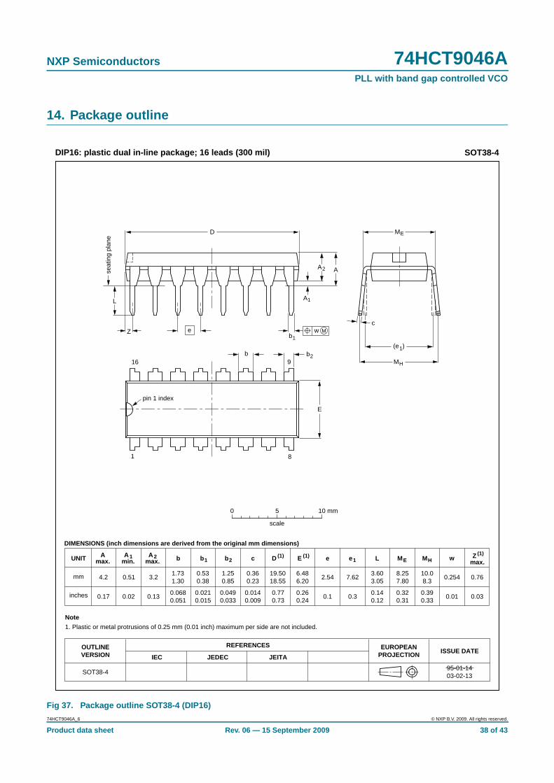
14. Package outline
Fig 37. Package outline SOT38-4 (DIP16)
REFERENCESOUTLINEVERSION
EUROPEANPROJECTION ISSUE DATE
IEC JEDEC JEITA
SOT38-495-01-1403-02-13
MH
c
(e )1
ME
A
L
seat
ing
plan
e
A1
w Mb1
b2
e
D
A2
Z
16
1
9
8
E
pin 1 index
b
0 5 10 mm
scale
Note
1. Plastic or metal protrusions of 0.25 mm (0.01 inch) maximum per side are not included.
UNIT Amax.
1 2 b1(1) (1) (1)
b2 c D E e M ZHL
mm
DIMENSIONS (inch dimensions are derived from the original mm dimensions)
A min.
A max. b
max.wMEe1
1.731.30
0.530.38
0.360.23
19.5018.55
6.486.20
3.603.05
0.2542.54 7.628.257.80
10.08.3
0.764.2 0.51 3.2
inches 0.0680.051
0.0210.015
0.0140.009
1.250.85
0.0490.033
0.770.73
0.260.24
0.140.12
0.010.1 0.30.320.31
0.390.33
0.030.17 0.02 0.13
DIP16: plastic dual in-line package; 16 leads (300 mil) SOT38-4
74HCT9046A_6 © NXP B.V. 2009. All rights reserved.
Product data sheet Rev. 06 — 15 September 2009 38 of 43

NXP Semiconductors 74HCT9046APLL with band gap controlled VCO
Fig 38. Package outline SOT109-1 (SO16)
X
w M
θ
AA1
A2
bp
D
HE
Lp
Q
detail X
E
Z
e
c
L
v M A
(A )3
A
8
9
1
16
y
pin 1 index
UNITA
max. A1 A2 A3 bp c D (1) E(1) (1)e HE L L p Q Zywv θ
REFERENCESOUTLINEVERSION
EUROPEANPROJECTION ISSUE DATE
IEC JEDEC JEITA
mm
inches
1.750.250.10
1.451.25
0.250.490.36
0.250.19
10.09.8
4.03.8
1.276.25.8
0.70.6
0.70.3 8
0
o
o
0.25 0.1
DIMENSIONS (inch dimensions are derived from the original mm dimensions)
Note
1. Plastic or metal protrusions of 0.15 mm (0.006 inch) maximum per side are not included.
1.00.4
SOT109-199-12-2703-02-19
076E07 MS-012
0.0690.0100.004
0.0570.049
0.010.0190.014
0.01000.0075
0.390.38
0.160.15
0.05
1.05
0.0410.2440.228
0.0280.020
0.0280.012
0.01
0.25
0.01 0.0040.0390.016
0 2.5 5 mm
scale
SO16: plastic small outline package; 16 leads; body width 3.9 mm SOT109-1
74HCT9046A_6 © NXP B.V. 2009. All rights reserved.
Product data sheet Rev. 06 — 15 September 2009 39 of 43

NXP Semiconductors 74HCT9046APLL with band gap controlled VCO
Fig 39. Package outline SOT403-1 (TSSOP16)
UNIT A1 A2 A3 bp c D (1) E (2) (1)e HE L L p Q Zywv θ
REFERENCESOUTLINEVERSION
EUROPEANPROJECTION ISSUE DATE
IEC JEDEC JEITA
mm 0.150.05
0.950.80
0.300.19
0.20.1
5.14.9
4.54.3
0.656.66.2
0.40.3
0.400.06
80
o
o0.13 0.10.21
DIMENSIONS (mm are the original dimensions)
Notes
1. Plastic or metal protrusions of 0.15 mm maximum per side are not included.
2. Plastic interlead protrusions of 0.25 mm maximum per side are not included.
0.750.50
SOT403-1 MO-15399-12-2703-02-18
w Mbp
D
Z
e
0.25
1 8
16 9
θ
AA1
A2
Lp
Q
detail X
L
(A )3
HE
E
c
v M A
XA
y
0 2.5 5 mm
scale
TSSOP16: plastic thin shrink small outline package; 16 leads; body width 4.4 mm SOT403-1
Amax.
1.1
pin 1 index
74HCT9046A_6 © NXP B.V. 2009. All rights reserved.
Product data sheet Rev. 06 — 15 September 2009 40 of 43

NXP Semiconductors 74HCT9046APLL with band gap controlled VCO
15. Abbreviations
16. Revision history
Table 11. Abbreviations
Acronym Description
CMOS Complementary Metal Oxide Semiconductor
DUT Device Under Test
ESD ElectroStatic Discharge
HBM Human Body Model
MM Machine Model
PLL Phase Locked Loop
VCO Voltage Controlled Oscillator
Table 12. Revision history
Document ID Release date Data sheet status Change notice Supersedes
74HCT9046A_6 20090915 Product data sheet - 74HCT9046A_5
Modifications: • The format of this data sheet has been redesigned to comply with the new identityguidelines of NXP Semiconductors.
• Legal texts have been adapted to the new company name where appropriate.
• Vi(p-p) value changed from 15 mV to 50 mV in Section 12.
• ∆f/∆T value moved from minimum to typical column Section 12.
• Package version SOT38-1 changed to SOT38-4 in Section 4 and Figure 37.
74HCT9046A_5 20031030 Product specification - 74HCT9046A_4
74HCT9046A_4 20030515 Product specification - 74HCT9046A_3
74HCT9046A_3 19990111 Product specification - -
74HCT9046A_6 © NXP B.V. 2009. All rights reserved.
Product data sheet Rev. 06 — 15 September 2009 41 of 43

NXP Semiconductors 74HCT9046APLL with band gap controlled VCO
17. Legal information
17.1 Data sheet status
[1] Please consult the most recently issued document before initiating or completing a design.
[2] The term ‘short data sheet’ is explained in section “Definitions”.
[3] The product status of device(s) described in this document may have changed since this document was published and may differ in case of multiple devices. The latest product statusinformation is available on the Internet at URL http://www.nxp.com.
17.2 Definitions
Draft — The document is a draft version only. The content is still underinternal review and subject to formal approval, which may result inmodifications or additions. NXP Semiconductors does not give anyrepresentations or warranties as to the accuracy or completeness ofinformation included herein and shall have no liability for the consequences ofuse of such information.
Short data sheet — A short data sheet is an extract from a full data sheetwith the same product type number(s) and title. A short data sheet is intendedfor quick reference only and should not be relied upon to contain detailed andfull information. For detailed and full information see the relevant full datasheet, which is available on request via the local NXP Semiconductors salesoffice. In case of any inconsistency or conflict with the short data sheet, thefull data sheet shall prevail.
17.3 Disclaimers
General — Information in this document is believed to be accurate andreliable. However, NXP Semiconductors does not give any representations orwarranties, expressed or implied, as to the accuracy or completeness of suchinformation and shall have no liability for the consequences of use of suchinformation.
Right to make changes — NXP Semiconductors reserves the right to makechanges to information published in this document, including withoutlimitation specifications and product descriptions, at any time and withoutnotice. This document supersedes and replaces all information supplied priorto the publication hereof.
Suitability for use — NXP Semiconductors products are not designed,authorized or warranted to be suitable for use in medical, military, aircraft,space or life support equipment, nor in applications where failure ormalfunction of an NXP Semiconductors product can reasonably be expectedto result in personal injury, death or severe property or environmental
damage. NXP Semiconductors accepts no liability for inclusion and/or use ofNXP Semiconductors products in such equipment or applications andtherefore such inclusion and/or use is at the customer’s own risk.
Applications — Applications that are described herein for any of theseproducts are for illustrative purposes only. NXP Semiconductors makes norepresentation or warranty that such applications will be suitable for thespecified use without further testing or modification.
Limiting values — Stress above one or more limiting values (as defined inthe Absolute Maximum Ratings System of IEC 60134) may cause permanentdamage to the device. Limiting values are stress ratings only and operation ofthe device at these or any other conditions above those given in theCharacteristics sections of this document is not implied. Exposure to limitingvalues for extended periods may affect device reliability.
Terms and conditions of sale — NXP Semiconductors products are soldsubject to the general terms and conditions of commercial sale, as publishedat http://www.nxp.com/profile/terms, including those pertaining to warranty,intellectual property rights infringement and limitation of liability, unlessexplicitly otherwise agreed to in writing by NXP Semiconductors. In case ofany inconsistency or conflict between information in this document and suchterms and conditions, the latter will prevail.
No offer to sell or license — Nothing in this document may be interpretedor construed as an offer to sell products that is open for acceptance or thegrant, conveyance or implication of any license under any copyrights, patentsor other industrial or intellectual property rights.
Export control — This document as well as the item(s) described hereinmay be subject to export control regulations. Export might require a priorauthorization from national authorities.
17.4 TrademarksNotice: All referenced brands, product names, service names and trademarksare the property of their respective owners.
18. Contact information
For more information, please visit: http://www .nxp.com
For sales office addresses, please send an email to: salesad [email protected]
Document status [1] [2] Product status [3] Definition
Objective [short] data sheet Development This document contains data from the objective specification for product development.
Preliminary [short] data sheet Qualification This document contains data from the preliminary specification.
Product [short] data sheet Production This document contains the product specification.
74HCT9046A_6 © NXP B.V. 2009. All rights reserved.
Product data sheet Rev. 06 — 15 September 2009 42 of 43

NXP Semiconductors 74HCT9046APLL with band gap controlled VCO
19. Contents
1 General description . . . . . . . . . . . . . . . . . . . . . . 12 Features . . . . . . . . . . . . . . . . . . . . . . . . . . . . . . . 13 Applications . . . . . . . . . . . . . . . . . . . . . . . . . . . . 24 Ordering information . . . . . . . . . . . . . . . . . . . . . 25 Block diagram . . . . . . . . . . . . . . . . . . . . . . . . . . 36 Functional diagram . . . . . . . . . . . . . . . . . . . . . . 37 Pinning information . . . . . . . . . . . . . . . . . . . . . . 57.1 Pinning . . . . . . . . . . . . . . . . . . . . . . . . . . . . . . . 57.2 Pin description . . . . . . . . . . . . . . . . . . . . . . . . . 58 Functional description . . . . . . . . . . . . . . . . . . . 68.1 Differences with respect to the familiar
74HCT4046A . . . . . . . . . . . . . . . . . . . . . . . . . . 68.2 VCO . . . . . . . . . . . . . . . . . . . . . . . . . . . . . . . . . 78.3 Phase comparators. . . . . . . . . . . . . . . . . . . . . . 78.3.1 Phase Comparator 1 (PC1) . . . . . . . . . . . . . . . 78.3.2 Phase Comparator 2 (PC2) . . . . . . . . . . . . . . . 98.4 Loop filter component selection . . . . . . . . . . . 139 Limiting values. . . . . . . . . . . . . . . . . . . . . . . . . 1410 Recommended operating conditions. . . . . . . 1511 Static characteristics. . . . . . . . . . . . . . . . . . . . 1512 Dynamic characteristics . . . . . . . . . . . . . . . . . 2013 Application information. . . . . . . . . . . . . . . . . . 2713.1 Filter design considerations for PC1 and
PC2 of the 74HCT9046A . . . . . . . . . . . . . . . . 2913.2 PLL design example . . . . . . . . . . . . . . . . . . . . 3313.3 Further information . . . . . . . . . . . . . . . . . . . . . 3714 Package outline . . . . . . . . . . . . . . . . . . . . . . . . 3815 Abbreviations . . . . . . . . . . . . . . . . . . . . . . . . . . 4116 Revision history . . . . . . . . . . . . . . . . . . . . . . . . 4117 Legal information. . . . . . . . . . . . . . . . . . . . . . . 4217.1 Data sheet status . . . . . . . . . . . . . . . . . . . . . . 4217.2 Definitions . . . . . . . . . . . . . . . . . . . . . . . . . . . . 4217.3 Disclaimers . . . . . . . . . . . . . . . . . . . . . . . . . . . 4217.4 Trademarks . . . . . . . . . . . . . . . . . . . . . . . . . . . 4218 Contact information. . . . . . . . . . . . . . . . . . . . . 4219 Contents . . . . . . . . . . . . . . . . . . . . . . . . . . . . . . 43
© NXP B.V. 2009. All rights reserved.For more information, please visit: http://www.nxp.comFor sales office addresses, please send an email to: [email protected]
Date of release: 15 September 2009
Document identifier: 74HCT9046A_6
Please be aware that important notices concerning this document and the product(s)described herein, have been included in section ‘Legal information’.