SCIPP Large-Scale Application of Silicon Detectors in...
95
Firenze 2001: Silicon Detectors Hartmut F.-W. Sadrozinski , SCIPP, UC Santa Cruz SCIPP Large-Scale Application of Silicon Detectors in Space Hartmut F.-W. Sadrozinski Santa Cruz Institute for Particle Physics (SCIPP) Development of Silicon Detectors GLAST : •Gamma-Ray •Large Area •Space Telescope
Transcript of SCIPP Large-Scale Application of Silicon Detectors in...
Firenze 2001: Silicon Detectors Hartmut F.-W. Sadrozinski , SCIPP, UC Santa Cruz
SCIPPSCIPP
Large-Scale Application of Silicon Detectorsin Space
Hartmut F.-W. SadrozinskiSanta Cruz Institute for Particle Physics (SCIPP)
Development of Silicon DetectorsGLAST :•Gamma-Ray •Large Area •Space Telescope
Firenze 2001: Silicon Detectors Hartmut F.-W. Sadrozinski , SCIPP, UC Santa Cruz
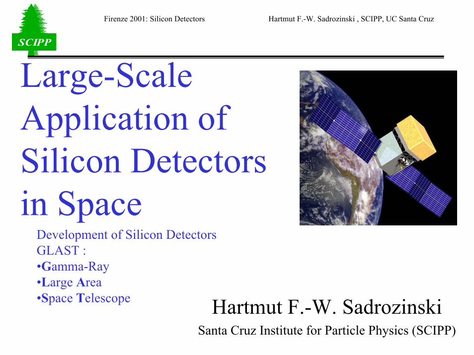
SCIPPSCIPP Principle of Silicon Strip Detectors
25-200 µm
300-400 µm
Alat ~ 100V
n+ implant
Al SiO2
p+ implantat ground
Depletion region. Charged particletraversing region produces ~80electron/hole pairs per micron.
Readout electronics(S/N typically > 20)
holes
Reverse Bias of junction: thermal current generationScale : Band gap 1.12eV vs. kT = 1/40eVCooling needed only in ultra-low noise applications.Wafer thickness 300um = 24k e-h pairs = 0.3%RLDepletion Voltage ~ thickness2 <100V Collection Time of e-h pairs: ~30nsArea is given by wafer size: 4” & 6” => Ladders
Firenze 2001: Silicon Detectors Hartmut F.-W. Sadrozinski , SCIPP, UC Santa Cruz
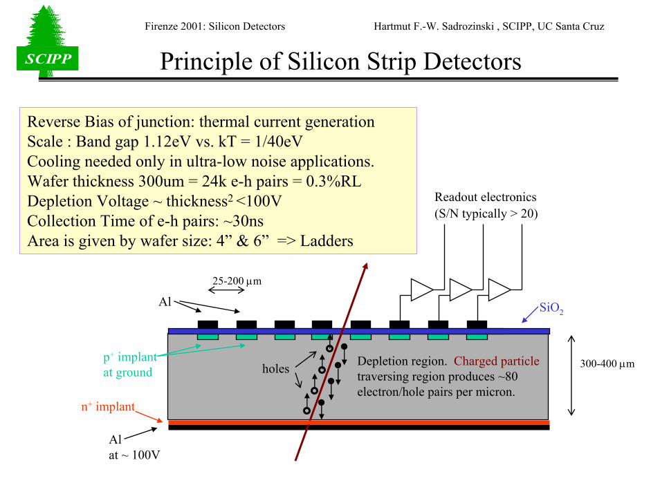
SCIPPSCIPP Evolution of Silicon Detectors
Large Area Double-sided
Hybrid Pixels
Monolythic:CCD, MAP
Si Drift
3-D
n n n
nn
p p
n
Firenze 2001: Silicon Detectors Hartmut F.-W. Sadrozinski , SCIPP, UC Santa Cruz
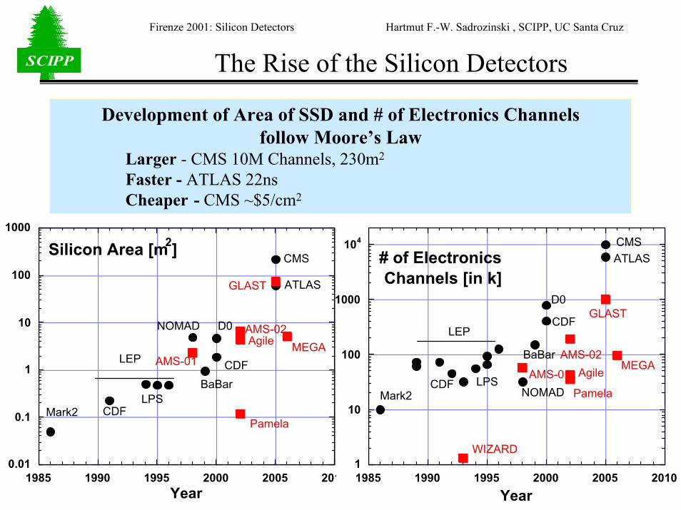
SCIPPSCIPP The Rise of the Silicon Detectors
Development of Area of SSD and # of Electronics Channels follow Moore’s Law
Larger - CMS 10M Channels, 230m2
Faster - ATLAS 22nsCheaper - CMS ~$5/cm2
0.01
0.1
1
10
100
1000
1985 1990 1995 2000 2005 201
Silicon Area [m2]
Year
CDF
ATLASGLAST
CMS
AMS-02
AMS-01
D0
BaBar
NOMAD
LEP
LPSCDFMark2
Pamela
Agile MEGA
1
10
100
1000
104
1985 1990 1995 2000 2005 2010
# of Electronics Channels [in k]
Year
CDF
ATLAS
GLAST
CMS
AMS-02
AMS-01
WIZARD
D0
BaBar
NOMAD
LEP
LPSCDFMark2 Pamela
Agile MEGA
Firenze 2001: Silicon Detectors Hartmut F.-W. Sadrozinski , SCIPP, UC Santa Cruz
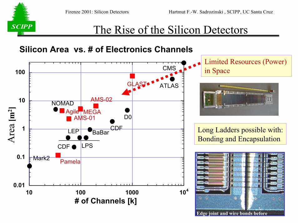
SCIPPSCIPP The Rise of the Silicon Detectors
Edge joint and wire bonds before encapsulation
0.01
0.1
1
10
100
10 100 1000 104
Silicon Area vs. # of Electronics Channels
# of Channels [k]
CDF
ATLASGLAST
CMS
AMS-02
AMS-01 D0
BaBar
NOMAD
LEP
LPSCDF
Mark2 Pamela
Agile MEGA
Are
a[m
2 ]
Limited Resources (Power) in Space
Long Ladders possible with:Bonding and Encapsulation
Firenze 2001: Silicon Detectors Hartmut F.-W. Sadrozinski , SCIPP, UC Santa Cruz
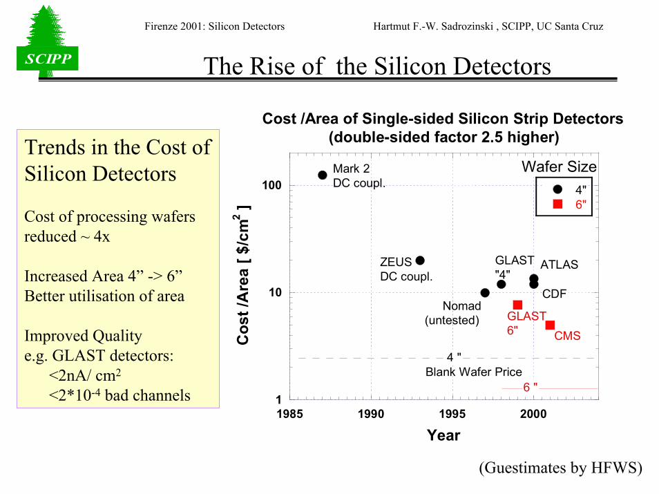
SCIPPSCIPP The Rise of the Silicon Detectors
Trends in the Cost of Silicon Detectors
Cost of processing wafers reduced ~ 4x
Increased Area 4” -> 6”Better utilisation of area
Improved Qualitye.g. GLAST detectors:
<2nA/ cm2
<2*10-4 bad channels 1
10
100
1985 1990 1995 2000
Cost /Area of Single-sided Silicon Strip Detectors(double-sided factor 2.5 higher)
4"6"
Cos
t /A
rea
[ $/c
m2 ]
Year
Mark 2DC coupl.
ZEUSDC coupl.
CDFNomad
(untested)
GLAST"4"
ATLAS
GLAST6"
Wafer Size
Blank Wafer Price4 "
6 "
CMS
(Guestimates by HFWS)
Firenze 2001: Silicon Detectors Hartmut F.-W. Sadrozinski , SCIPP, UC Santa Cruz
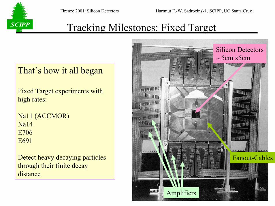
SCIPPSCIPP Tracking Milestones: Fixed Target
Silicon Detectors~ 5cm x5cm
Fanout-Cables
Amplifiers
That’s how it all began
Fixed Target experiments withhigh rates:
Na11 (ACCMOR)Na14E706E691
Detect heavy decaying particles through their finite decay distance

Firenze 2001: Silicon Detectors Hartmut F.-W. Sadrozinski , SCIPP, UC Santa Cruz
SCIPPSCIPP Tracking Milestones: Vertex Detectors
The big step forward in Mark2:ASIC’s (Terry Walker et al)
Vertex Detector ParadigmASIC’s,Few thin layers,Close in.
ALEPH
Every LEP Experiment has aVertex Detectors:
Double-SidedAC-coupled

Firenze 2001: Silicon Detectors Hartmut F.-W. Sadrozinski , SCIPP, UC Santa Cruz
SCIPPSCIPP Tracking Milestones: Speed and Rad.Hardness
56 planes, 50k channelsElliptical shapes!
2 chip set: Bipolar+CMOS
LPS at HERA (UC Santa Cruz & INFN)“Fixed Target” at ColliderImportance of Electronics:
rad hardfastlow noiselow power
Firenze 2001: Silicon Detectors Hartmut F.-W. Sadrozinski , SCIPP, UC Santa Cruz
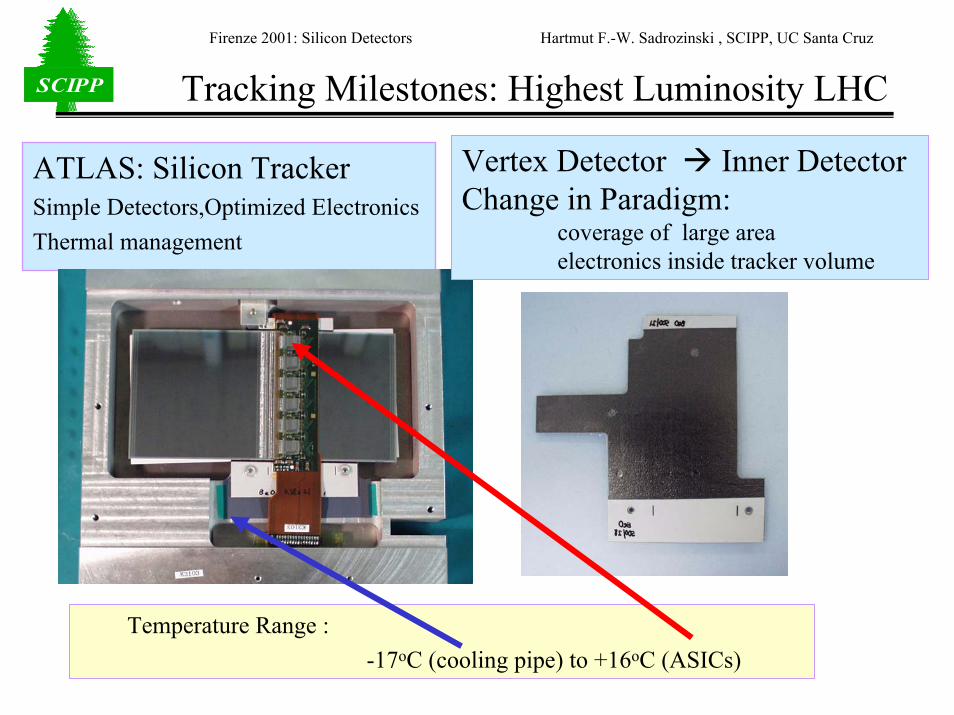
SCIPPSCIPP Tracking Milestones: Highest Luminosity LHC
Temperature Range : -17oC (cooling pipe) to +16oC (ASICs)
Vertex Detector Inner DetectorChange in Paradigm:
coverage of large areaelectronics inside tracker volume
ATLAS: Silicon TrackerSimple Detectors,Optimized ElectronicsThermal management
Firenze 2001: Silicon Detectors Hartmut F.-W. Sadrozinski , SCIPP, UC Santa Cruz
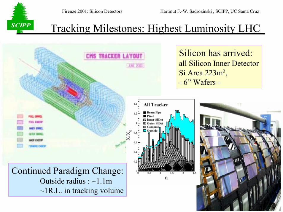
SCIPPSCIPP Tracking Milestones: Highest Luminosity LHC
Continued Paradigm Change:Outside radius : ~1.1m~1R.L. in tracking volume
Silicon has arrived:all Silicon Inner DetectorSi Area 223m2, - 6” Wafers -
Firenze 2001: Silicon Detectors Hartmut F.-W. Sadrozinski , SCIPP, UC Santa Cruz
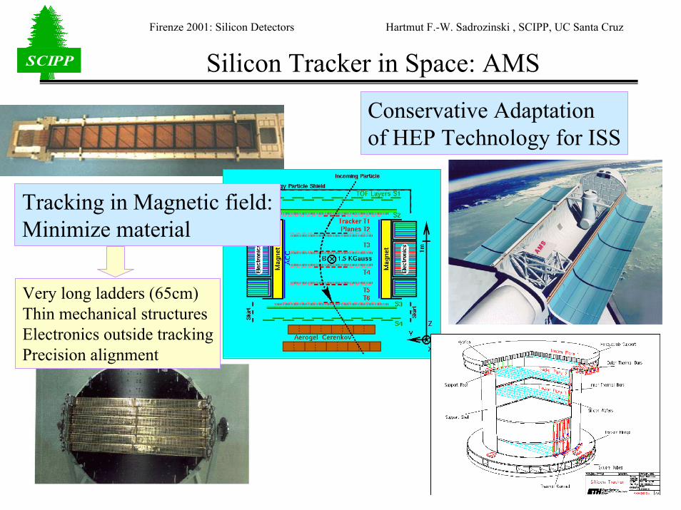
SCIPPSCIPP Silicon Tracker in Space: AMS
Very long ladders (65cm)Thin mechanical structuresElectronics outside trackingPrecision alignment
Tracking in Magnetic field:Minimize material
Conservative Adaptation of HEP Technology for ISS
Firenze 2001: Silicon Detectors Hartmut F.-W. Sadrozinski , SCIPP, UC Santa Cruz
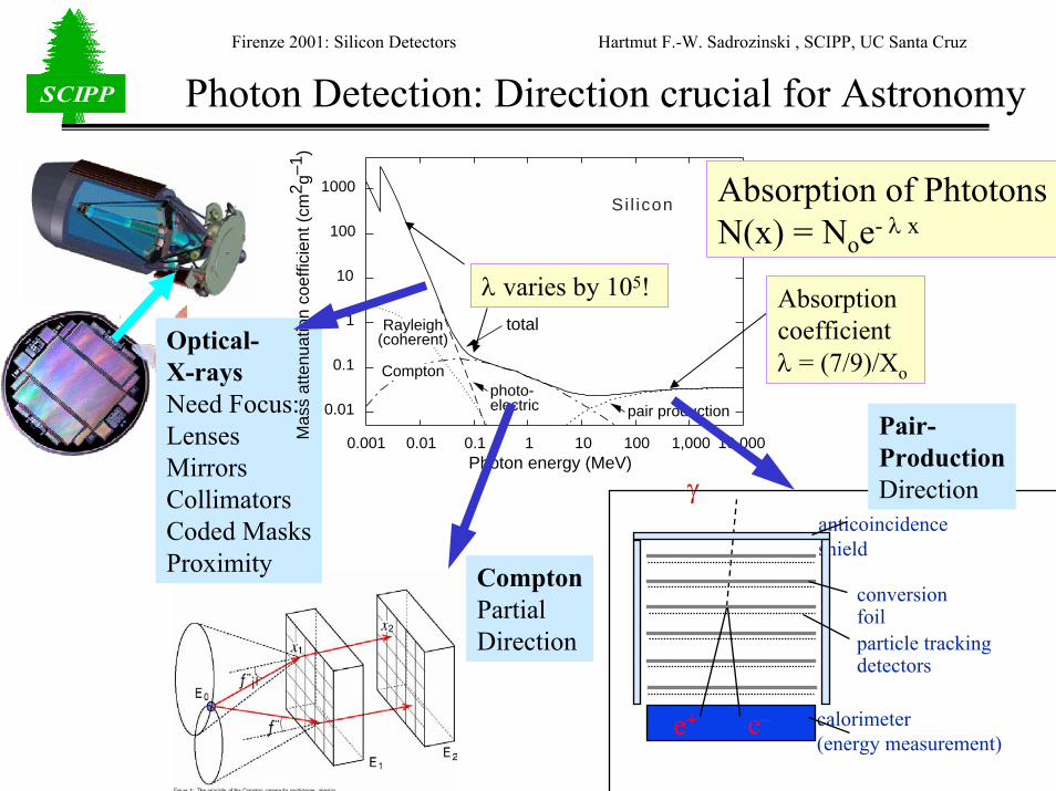
SCIPPSCIPP Photon Detection: Direction crucial for Astronomy
Optical-X-raysNeed Focus:LensesMirrorsCollimatorsCoded MasksProximity
Photon energy (MeV)
1
0.01
0.1
10
100
1000
Mas
s at
tenu
atio
n co
effic
ient
(cm
2 g–1
)
photo-electric pair production
total
Si l icon
0.10.010.001 1 10 100 1,000 10,000
Rayleigh(coherent)
Compton
λ varies by 105!
Absorption of PhtotonsN(x) = Noe- λ x
ComptonPartial Direction
γ
calorimeter (energy measurement)
anticoincidenceshield
e+ e–
particle tracking detectors
conversion foil
Pair-ProductionDirection
Absorption coefficientλ = (7/9)/Xo

Firenze 2001: Silicon Detectors Hartmut F.-W. Sadrozinski , SCIPP, UC Santa Cruz
SCIPPSCIPP Application: Compton Telescope AstroPhysics
Reduced Compton circles of events with electron track
MEGAUse of electron directionto limit the Compton cone.
Stack of Silicon detectors
MPE - NRL
Multiple Compton +Energy Measurement
Classical Compton Event Circles
Firenze 2001: Silicon Detectors Hartmut F.-W. Sadrozinski , SCIPP, UC Santa Cruz
SCIPPSCIPPEGRET / GLAST / AGILE: Pair Conversion Telescope
γ
e+ e- calorimeter (energy measurement)
particle tracking detectors
conversion foils
charged particle anticoincidence shield
1
2
Converter Thickness tConversion Probability ~ tPointing RMS ~ √t
Gamma-rays convert into e+e- pairs,are tracked and their energy measuredGamma is reconstructed from e+e- tracks
MaximizeNumber of Converters
New Paradigm:Add material into tracking volume:
Firenze 2001: Silicon Detectors Hartmut F.-W. Sadrozinski , SCIPP, UC Santa Cruz
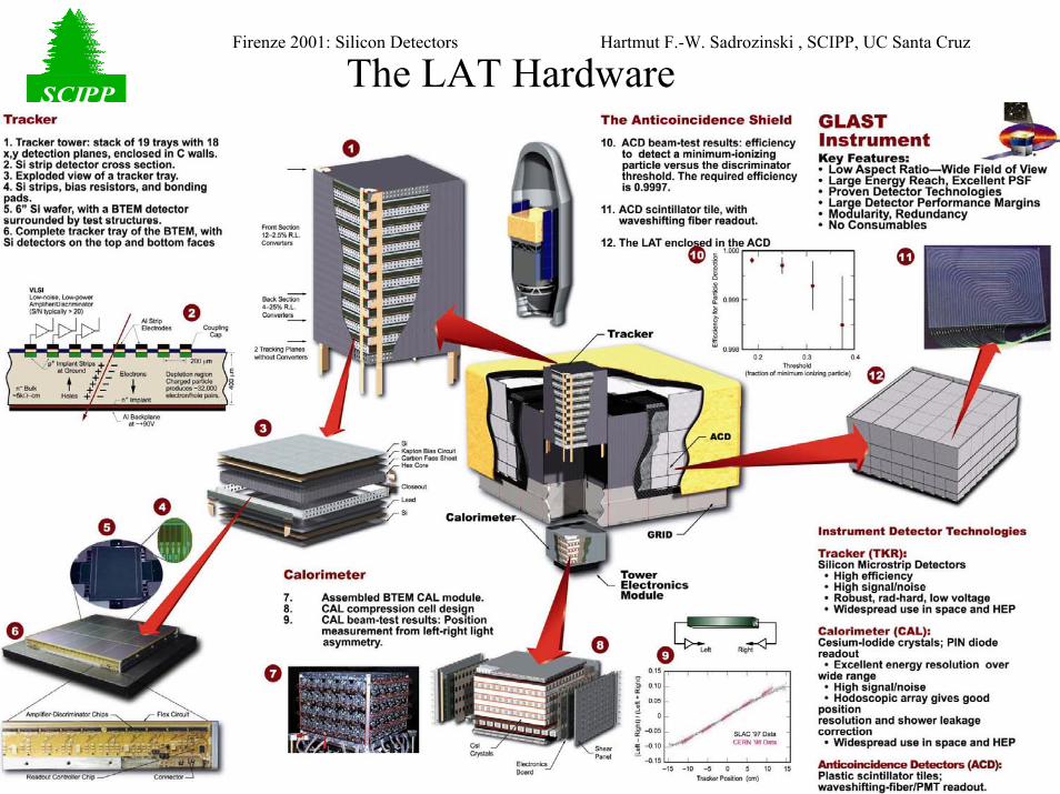
SCIPPSCIPP GLAST Gamma-Ray Large Area Space TelescopeAn Astro-Particle Physics Partnership Exploring the High-Energy Universe
• Precision Si-strip Tracker (TKR)• Hodoscopic CsI Calorimeter (CAL)• Segmented Anticoincidence Detector (ACD)• Advantages of modular design• NASA, DoE, DoD, INFN/ASI, Japan, CEA, IN2P3, Sweden
Challenges of Science in Space
• Launch
• Limited Resources• Space Environment
4 x 4 Arrayof Towers
AnticoincidenceShield
CalorimeterModule
Grid
TrackerModule
GammaRay
Resolving the γ-ray sky
Design Optimized for Key Science Objectives
• Understand particle acceleration in AGN, Pulsars, & SNRs• Resolve the γ-ray sky: unidentified sources & diffuse emission• Determine the high-energy behavior of GRBs & Transients
Proven technologies and 7 years of design, development and demonstration efforts
Firenze 2001: Silicon Detectors Hartmut F.-W. Sadrozinski , SCIPP, UC Santa Cruz
SCIPPSCIPP GLAST LAT: International Collaboration• expertise in each science topic (theory + obs.)• experience in high-energy and space instrumentation• access to X-ray, MeV, and TeV observatories by
collaboration for multi-wavelength observations
• expertise in each science topic (theory + obs.)• experience in high-energy and space instrumentation• access to X-ray, MeV, and TeV observatories by
collaboration for multi-wavelength observations
~ 100 collaboratorsfrom 28 institutions
~ 100 collaboratorsfrom 28 institutions
Organizations with LAT Hardware Involvement
Stanford University & Stanford Linear Accelerator CenterNASA Goddard Space Flight CenterNaval Research LaboratoryUniversity of California at Santa CruzUniversity of Washington
Commissariat a l’Energie Atomique, Departement d’Astrophysique (CEA)Institut National de Physique Nuclearie et de Physique des Particules (IN2P3): Ecole Polytechnique, College de France, CENBG (Bordeaux)
Hiroshima UniversityInstitute of Space and Astronautical Science, TokyoRIKENTokyo Institute of Technology
Istituto Nazionale di Fisica Nucleare (INFN): Pisa, Trieste, Bari, Udine, Perugia, Roma
Royal Institute of Technology (KTH), Stockholm
TKRCALACD
CAL
TKR
TKR
CAL
Firenze 2001: Silicon Detectors Hartmut F.-W. Sadrozinski , SCIPP, UC Santa Cruz
SCIPPSCIPP GLAST LAT: International Collaboration
EGRET ~10
GLAST ~100
ATLAS/CMS ~1000
Firenze 2001: Silicon Detectors Hartmut F.-W. Sadrozinski , SCIPP, UC Santa Cruz
SCIPPSCIPP GLAST LAT TKR Collaboration
Organization of the LAT TKR Subsystem Activities
University of California at Santa CruzManagementFront-end Electronics
Stanford University & Stanford Linear Accelerator CenterFront-end ElectronicI & T
Hiroshima UniversitySSD
Istituto Nazionale di Fisica Nucleare (INFN): Pisa, Trieste, Bari, Udine, Perugia, Roma
MechanicsAssemblyTower I&T

Firenze 2001: Silicon Detectors Hartmut F.-W. Sadrozinski , SCIPP, UC Santa Cruz
SCIPPSCIPP Criteria for large-scale Application in Space
FlexibilityAdapt to Space Environment (low power, light weight, rigid, radiation, inaccessibility)Use Conservative (“proven”) Approach
ModularityClean InterfacesLowered Risk in Performance and Schedule
SimplicitySimple, controlled AssemblyRobust Detectors and Electronics
RedundancyNo single-point Failures
Q/AParts SelectionProcedures – Work with IndustryEarly R&DTesting
Firenze 2001: Silicon Detectors Hartmut F.-W. Sadrozinski , SCIPP, UC Santa Cruz
SCIPPSCIPP The Large Area Telescope (LAT)
DAQ Electronics
Grid
Tracker
Calorimeter
ACD Thermal Blanket
•Array of 16 identical “Tower” Modules, each with a tracker (Si strips) and a calorimeter (CsI with PIN diode readout) and DAQ module.
•Surrounded by finely segmented ACD(plastic scintillator with PMT readout).
•Aluminum strong-back “Grid,” with heat pipes for transport of heat to the instrument sides.
Firenze 2001: Silicon Detectors Hartmut F.-W. Sadrozinski , SCIPP, UC Santa Cruz
SCIPPSCIPP Overview of TKR Tower Design
• 16 towers, each with 37 cm × 37 cm of Si (78m2 in all)
• 18 x,y planes per tower– 19 “tray” structures ~3cm high
• Si planes on top and bottom• 12 with 3% W converter on bottom• 4 with 18% W converter on bottom• 2 with no converter
– Every other tray rotated by 90°, so each W foil is followed immediately by an x,y plane
• 2mm gap between x and y• Electronics on the sides of trays
– Minimize gap between towers– 9 readout modules on each of 4 sides
• Trays stack and align at their corners• The bottom tray has a flange to mount on
the grid• Carbon-fiber walls provide stiffness and the
thermal pathway to the grid (∆T~11oC)
Carbon thermal
panel
Readout Cable
Electronics Module
2 mm gapCarbon-Fiber Wall
19 Carbon-Fiber Tray Panels
Firenze 2001: Silicon Detectors Hartmut F.-W. Sadrozinski , SCIPP, UC Santa Cruz
SCIPPSCIPP 2 Clean Interfaces per TKR Tower
4.1.4.3.1Silicon-Strip
Detectors
4.1.4.3.2Tray Mechanical
C-fiber panelW converters
4.1.4.3.3Tray Electronics (MCM)
F.E. ASIC; Controller ASIC; PC Board;Connector sockets; Pitch Adapter; Passive parts
4.1.4.4.1Tower Structure
C-fiber sidewallsFasteners
Spacers/pinsEMI shield
4.1.4.4.2Tower Cable Plant
Flexible multi-layer cables; Connector Plugs
Wire BondsScrews;
Adhesive tape
BiasCircuit;
Adhesive
Det
ecto
r Bia
s
Wire
Bon
ds
Nano- Connectors Machined
Cable RunsFasteners
TowerElectronics
Module
GridFlexure Mount
ThermalGasket
GLAST TrackerBlock Diagram
andInterfaces
Mechanical
ElectricalNo Inter-Tower Interfaces
Firenze 2001: Silicon Detectors Hartmut F.-W. Sadrozinski , SCIPP, UC Santa Cruz
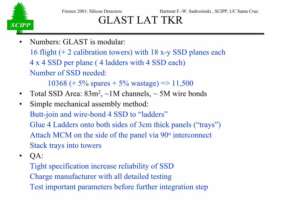
SCIPPSCIPP GLAST LAT TKR
• Numbers: GLAST is modular:16 flight (+ 2 calibration towers) with 18 x-y SSD planes each4 x 4 SSD per plane ( 4 ladders with 4 SSD each)Number of SSD needed:
10368 (+ 5% spares + 5% wastage) => 11,500 • Total SSD Area: 83m2, ~1M channels, ~ 5M wire bonds• Simple mechanical assembly method:
Butt-join and wire-bond 4 SSD to “ladders”Glue 4 Ladders onto both sides of 3cm thick panels (“trays”) Attach MCM on the side of the panel via 90o interconnect Stack trays into towers
• QA:Tight specification increase reliability of SSDCharge manufacturer with all detailed testingTest important parameters before further integration step
Firenze 2001: Silicon Detectors Hartmut F.-W. Sadrozinski , SCIPP, UC Santa Cruz
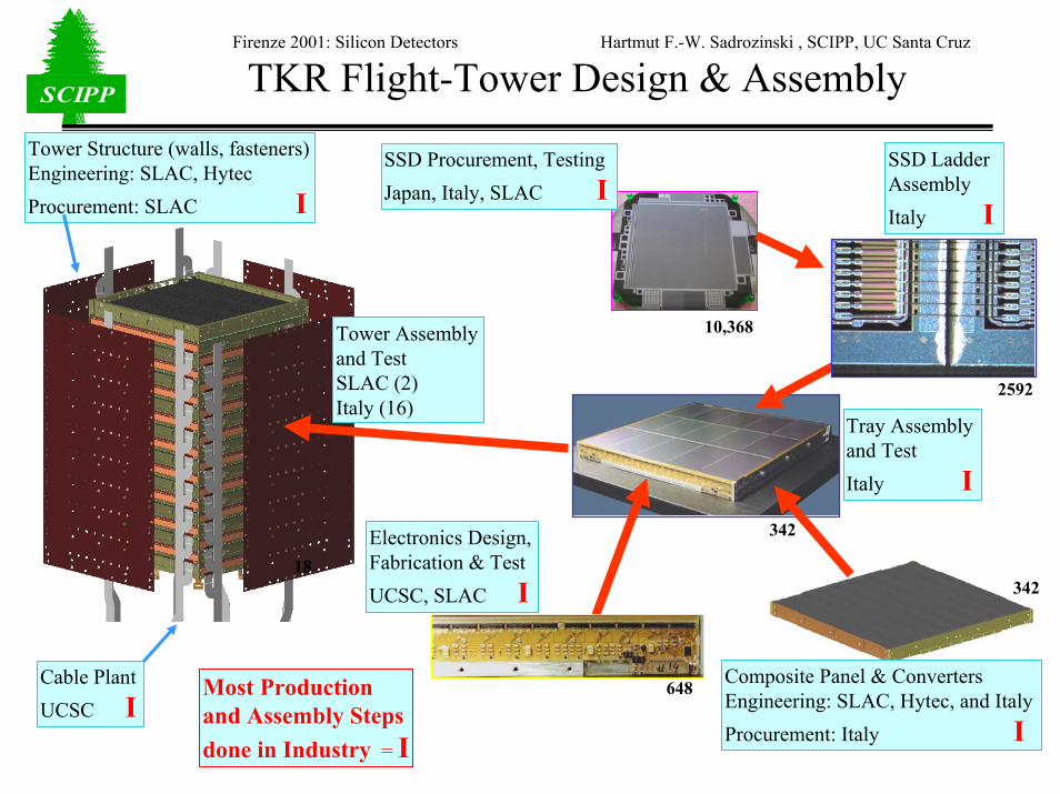
SCIPPSCIPP TKR Flight-Tower Design & Assembly
Cable PlantUCSC I
Tower Structure (walls, fasteners)Engineering: SLAC, HytecProcurement: SLAC I
Tower Assembly and TestSLAC (2) Italy (16)
Tray Assembly and TestItaly I
Composite Panel & ConvertersEngineering: SLAC, Hytec, and ItalyProcurement: Italy I
2592
342
648
34218
SSD Ladder AssemblyItaly I
SSD Procurement, TestingJapan, Italy, SLAC I
10,368
Electronics Design, Fabrication & TestUCSC, SLAC I
Most Production and Assembly Steps done in Industry = I
Firenze 2001: Silicon Detectors Hartmut F.-W. Sadrozinski , SCIPP, UC Santa Cruz
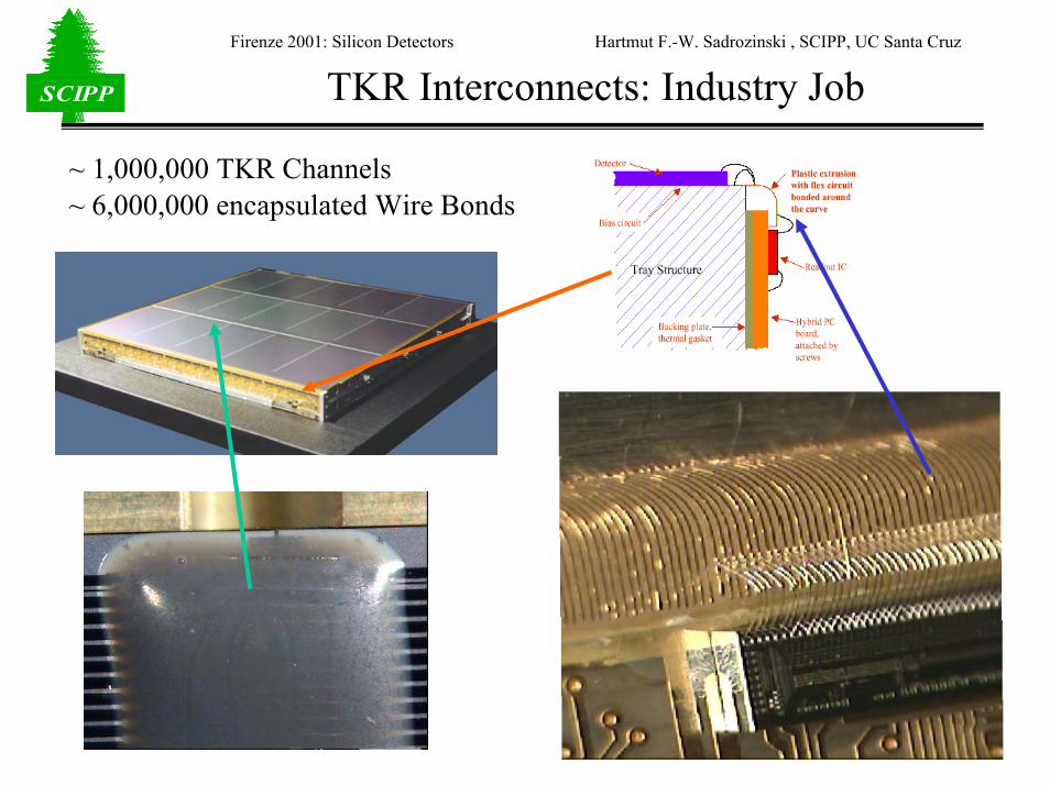
SCIPPSCIPP TKR Interconnects: Industry Job
~ 1,000,000 TKR Channels~ 6,000,000 encapsulated Wire Bonds
Firenze 2001: Silicon Detectors Hartmut F.-W. Sadrozinski , SCIPP, UC Santa Cruz
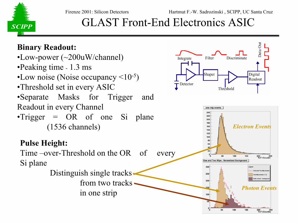
SCIPPSCIPP GLAST Front-End Electronics ASIC
Binary Readout: •Low-power (~200uW/channel) •Peaking time ˜ 1.3 ms•Low noise (Noise occupancy <10-5)•Threshold set in every ASIC•Separate Masks for Trigger and Readout in every Channel•Trigger = OR of one Si plane
(1536 channels)
Pulse Height:Time –over-Threshold on the OR of every Si plane
Distinguish single tracks from two tracks in one strip
Electron Events
Photon Events
Firenze 2001: Silicon Detectors Hartmut F.-W. Sadrozinski , SCIPP, UC Santa Cruz
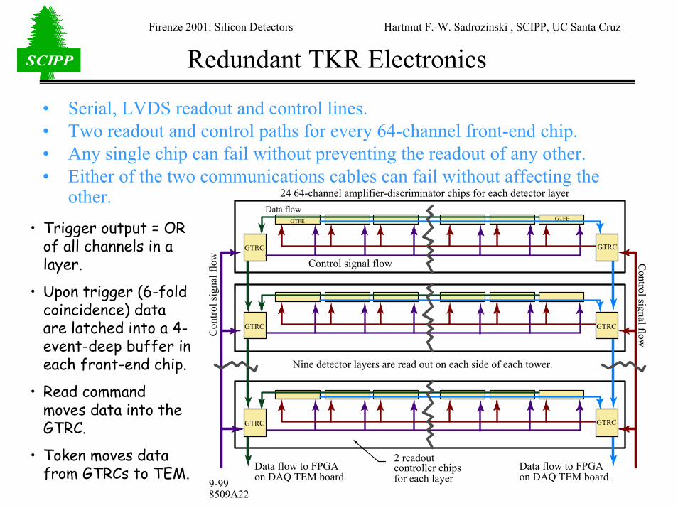
SCIPPSCIPP Redundant TKR Electronics
• Serial, LVDS readout and control lines.• Two readout and control paths for every 64-channel front-end chip.• Any single chip can fail without preventing the readout of any other.• Either of the two communications cables can fail without affecting the
other. 24 64-channel amplifier-discriminator chips for each detector layer
2 readoutcontroller chipsfor each layer
Con
trol s
igna
l flo
w Control signal flow
Data flow to FPGAon DAQ TEM board.
Data flow to FPGAon DAQ TEM board.
Control signal flow
Data flow
Nine detector layers are read out on each side of each tower.
GTRC
GTFEGTFE
GTRC
GTRC
GTRC
GTRC
GTRC
9-998509A22
• Trigger output = OR of all channels in a layer.
• Upon trigger (6-fold coincidence) data are latched into a 4-event-deep buffer in each front-end chip.
• Read command moves data into the GTRC.
• Token moves data from GTRCs to TEM.
Firenze 2001: Silicon Detectors Hartmut F.-W. Sadrozinski , SCIPP, UC Santa Cruz
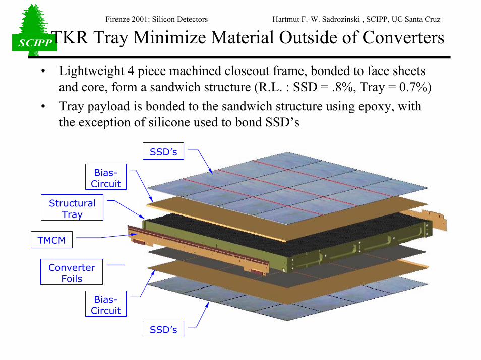
SCIPPSCIPPTKR Tray Minimize Material Outside of Converters
• Lightweight 4 piece machined closeout frame, bonded to face sheets and core, form a sandwich structure (R.L. : SSD = .8%, Tray = 0.7%)
• Tray payload is bonded to the sandwich structure using epoxy, with the exception of silicone used to bond SSD’s
Converter Foils
SSD’s
Bias-Circuit
Structural Tray
TMCM
Bias-Circuit
SSD’s
Firenze 2001: Silicon Detectors Hartmut F.-W. Sadrozinski , SCIPP, UC Santa Cruz
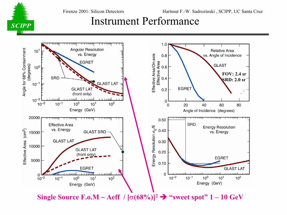
SCIPPSCIPP Instrument Performance
FOV: 2.4 srSRD: 2.0 sr
Single Source F.o.M ~ Aeff / [σ(68%)]2 “sweet spot” 1 – 10 GeV
Firenze 2001: Silicon Detectors Hartmut F.-W. Sadrozinski , SCIPP, UC Santa Cruz
SCIPPSCIPP GLAST LAT SSD
Firenze 2001: Silicon Detectors Hartmut F.-W. Sadrozinski , SCIPP, UC Santa Cruz
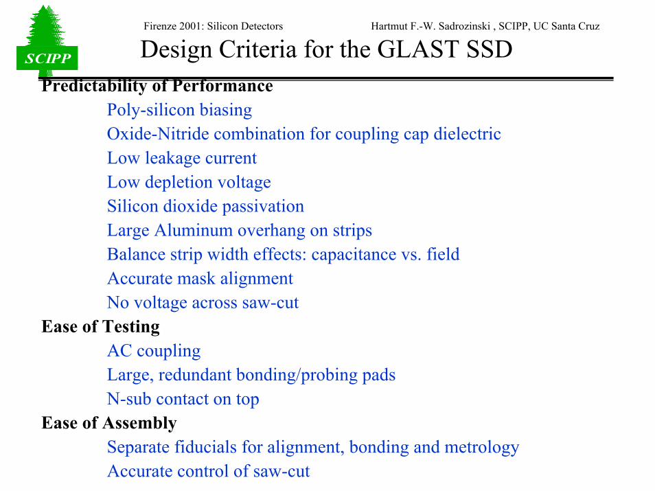
SCIPPSCIPP Design Criteria for the GLAST SSDPredictability of Performance
Poly-silicon biasingOxide-Nitride combination for coupling cap dielectricLow leakage currentLow depletion voltageSilicon dioxide passivationLarge Aluminum overhang on stripsBalance strip width effects: capacitance vs. fieldAccurate mask alignmentNo voltage across saw-cut
Ease of TestingAC couplingLarge, redundant bonding/probing padsN-sub contact on top
Ease of AssemblySeparate fiducials for alignment, bonding and metrologyAccurate control of saw-cut
Firenze 2001: Silicon Detectors Hartmut F.-W. Sadrozinski , SCIPP, UC Santa Cruz
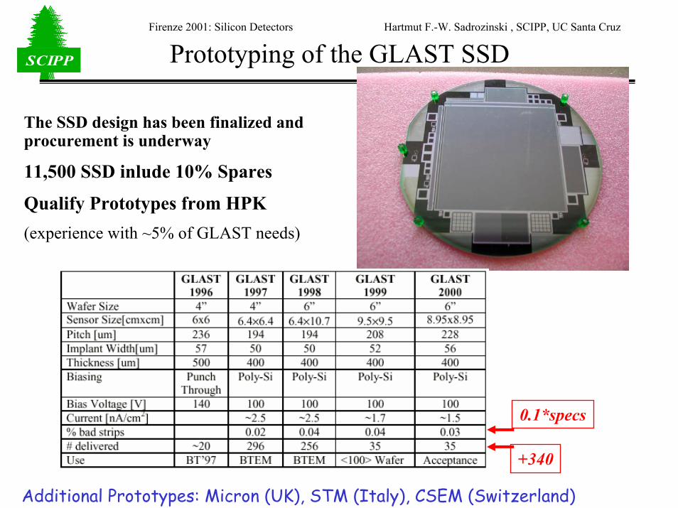
SCIPPSCIPP Prototyping of the GLAST SSD
The SSD design has been finalized and procurement is underway
11,500 SSD inlude 10% Spares
Qualify Prototypes from HPK (experience with ~5% of GLAST needs)
0.1*specs
+340
Additional Prototypes: Micron (UK), STM (Italy), CSEM (Switzerland)
Firenze 2001: Silicon Detectors Hartmut F.-W. Sadrozinski , SCIPP, UC Santa Cruz
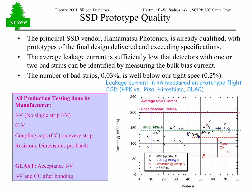
SCIPPSCIPPSSD Prototype Quality
• The principal SSD vendor, Hamamatsu Photonics, is already qualified, with prototypes of the final design delivered and exceeding specifications.
• The average leakage current is sufficiently low that detectors with one or two bad strips can be identified by measuring the bulk bias current.
• The number of bad strips, 0.03%, is well below our tight spec (0.2%).
0
50
100
150
200
250
0 10 20 30 40 50 60 70 80
HPK @25deg CSLAC @19deg CHIroshima @19deg CINFN Pisa
Wafer #
Average SSD Current
Specification: 200nA
HPK: 143nA
TempCorr.
Leakage current in nA measured on prototype flight SSD (HPK vs. Pisa, Hiroshima, SLAC)
All Production Testing done by Manufacturer:
I-V (No single strip I-V)
C-V
Coupling caps (CC) on every strip
Resistors, Dimensions per batch
GLAST: Acceptance I-V
I-V and CC after bonding

Firenze 2001: Silicon Detectors Hartmut F.-W. Sadrozinski , SCIPP, UC Santa Cruz
SCIPPSCIPP SSD Production Quality
0
50
100
150
200
250
50561 50563 50565 50567 50569 50571 50573
HPK 1rst + 2nd LotAverage Run Leakage current
5056250563505645056550566
5056750568505705057150572
Run #
Run #
< i > = 186 nA
0
20
40
60
80
100
120
50561 50563 50565 50567 50569 50
HPK 1rst & 2nd LotAverage Depletion Voltage
5056250563505645056550566
Run #
Run #
The first 320 Production SSDLeakage Current and Depletion Voltage
GLAST LAT Specifications;Ave current < 200nA Depletion Voltage <120VMax Current < 500nA
571 50573
5056750568505705057150572

Firenze 2001: Silicon Detectors Hartmut F.-W. Sadrozinski , SCIPP, UC Santa Cruz
SCIPPSCIPP Radiation Hardness
Test Total Dose Dependence of Leakage currents, CInterstrip, CBody, RBias, RInterstrip, Ccoupling
Up to 20kRad (1kRad predicted)
Heavy Ion Test of SEE Immunity of Coupling Cap: ok
Live Baby Skinny010203040506070
0 5 10 15
perimeter/area ratio [/cm2]Le
akag
e cu
rren
t [nA
/ cm
2 ]
0kRad 10kRad
Max spec10.2nA/cm2
Max spec afterirradiation120nA/cm2
Firenze 2001: Silicon Detectors Hartmut F.-W. Sadrozinski , SCIPP, UC Santa Cruz
SCIPPSCIPP Dimensional Tests on HPK SSD
Thickness
Saw Cut(Crucial for Assembly):
Spec at 20um.Average tiltnow 2um!
Planarity
0.5
0.4
0.3
0.2
0.1
0.0
Thickness (mm)
38
37
36
35
34
33
32
31
30
29
28
27
26
25
24
23
22
21
20
19
18
17
16
15
14
13
12
11
109876
Detector ID
HPK preseries
Measured capacitanceWill yield thickness for every SSD
Firenze 2001: Silicon Detectors Hartmut F.-W. Sadrozinski , SCIPP, UC Santa Cruz
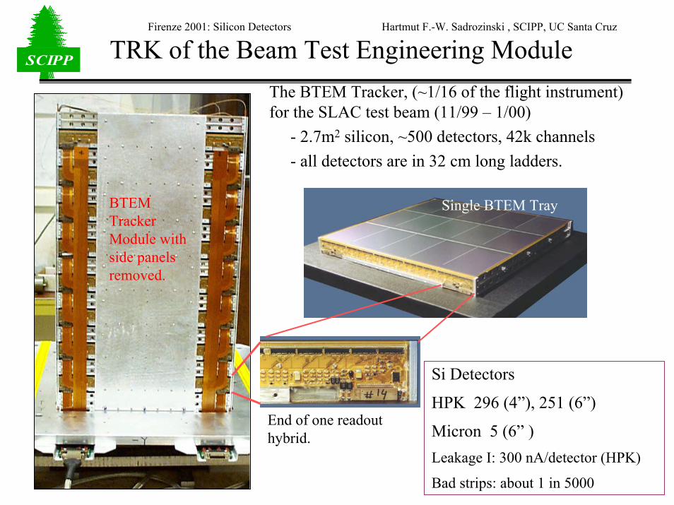
SCIPPSCIPP TRK of the Beam Test Engineering Module
End of one readout hybrid.
BTEM Tracker Module with side panels removed.
Single BTEM Tray
The BTEM Tracker, (~1/16 of the flight instrument) for the SLAC test beam (11/99 – 1/00)
- 2.7m2 silicon, ~500 detectors, 42k channels- all detectors are in 32 cm long ladders.
Si Detectors
HPK 296 (4”), 251 (6”)
Micron 5 (6” ) Leakage I: 300 nA/detector (HPK)
Bad strips: about 1 in 5000
Firenze 2001: Silicon Detectors Hartmut F.-W. Sadrozinski , SCIPP, UC Santa Cruz
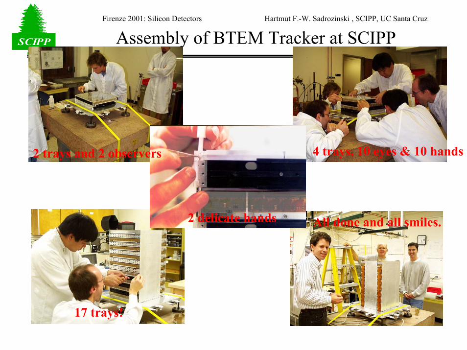
SCIPPSCIPP Assembly of BTEM Tracker at SCIPP
4 trays, 10 eyes & 10 hands
17 trays!
2 delicate hands
2 trays and 2 observers
All done and all smiles.
Firenze 2001: Silicon Detectors Hartmut F.-W. Sadrozinski , SCIPP, UC Santa Cruz
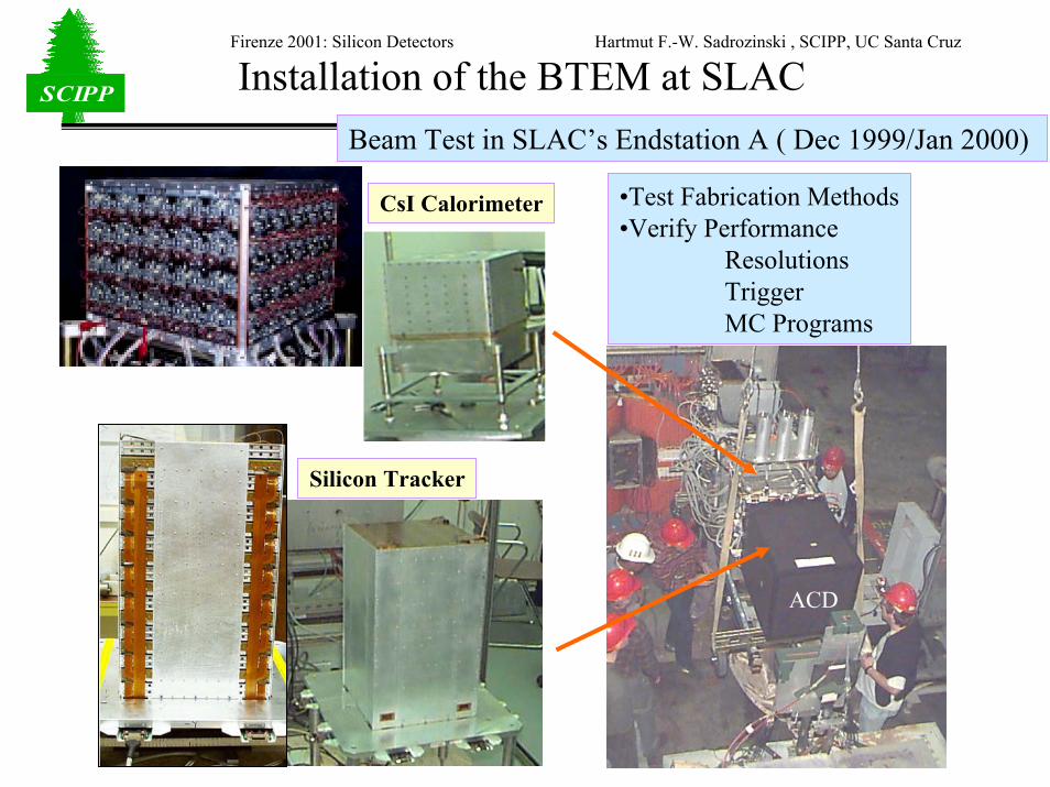
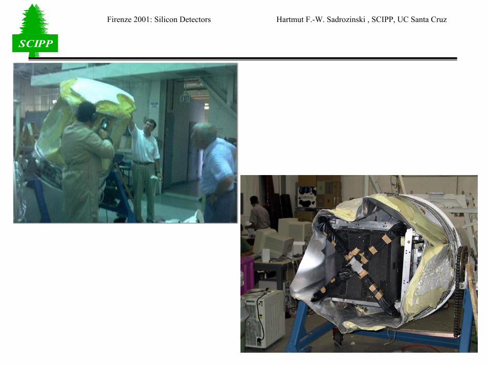
SCIPPSCIPP Installation of the BTEM at SLACBeam Test in SLAC’s Endstation A ( Dec 1999/Jan 2000)
Silicon Tracker
CsI Calorimeter
ACD
•Test Fabrication Methods•Verify Performance
ResolutionsTriggerMC Programs
Firenze 2001: Silicon Detectors Hartmut F.-W. Sadrozinski , SCIPP, UC Santa Cruz
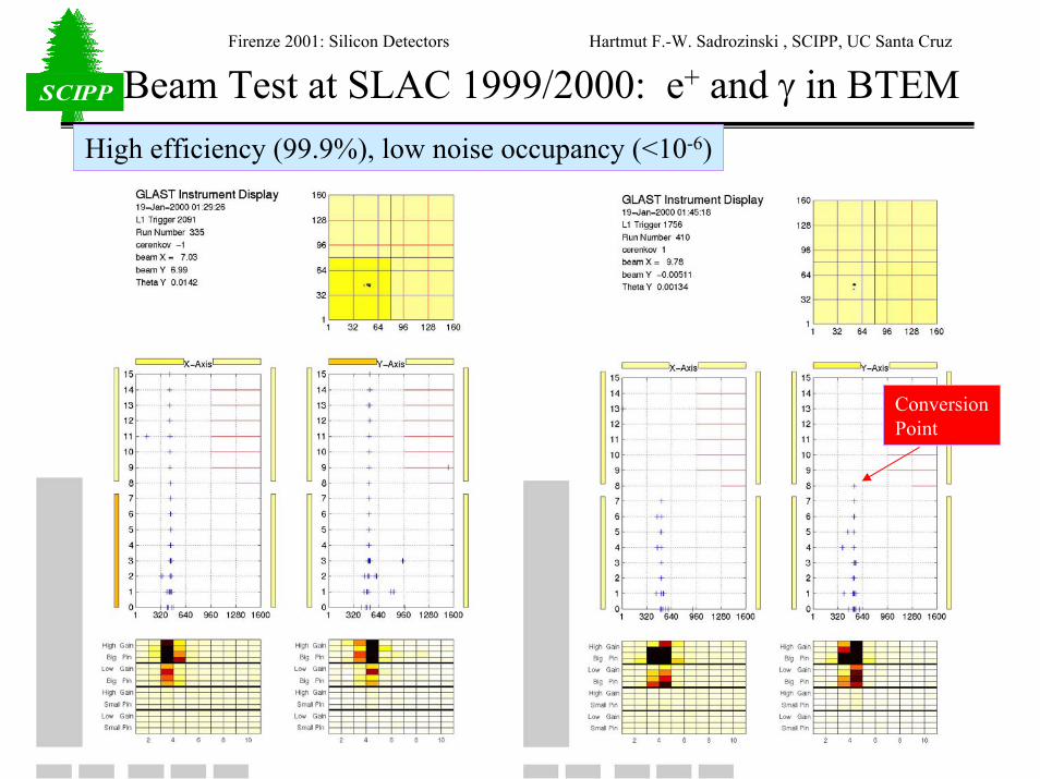
SCIPPSCIPP Beam Test at SLAC 1999/2000: e+ and γ in BTEMHigh efficiency (99.9%), low noise occupancy (<10-6)
ConversionPoint

Firenze 2001: Silicon Detectors Hartmut F.-W. Sadrozinski , SCIPP, UC Santa Cruz
SCIPPSCIPPEffective Area = Geometric Area * Conversion efficiency
PSFAeff ~ 6 % R.L
~ 25 % R.L
Back Section:3 layers of thickEfficient Conversionbefore calorimeter
Front Section:10 layers of thin converters:Precision Tracking
Effective Area:Vertex Distribution reflects the Converter Distributionshows expected Attenuation of the γ Beam
Firenze 2001: Silicon Detectors Hartmut F.-W. Sadrozinski , SCIPP, UC Santa Cruz
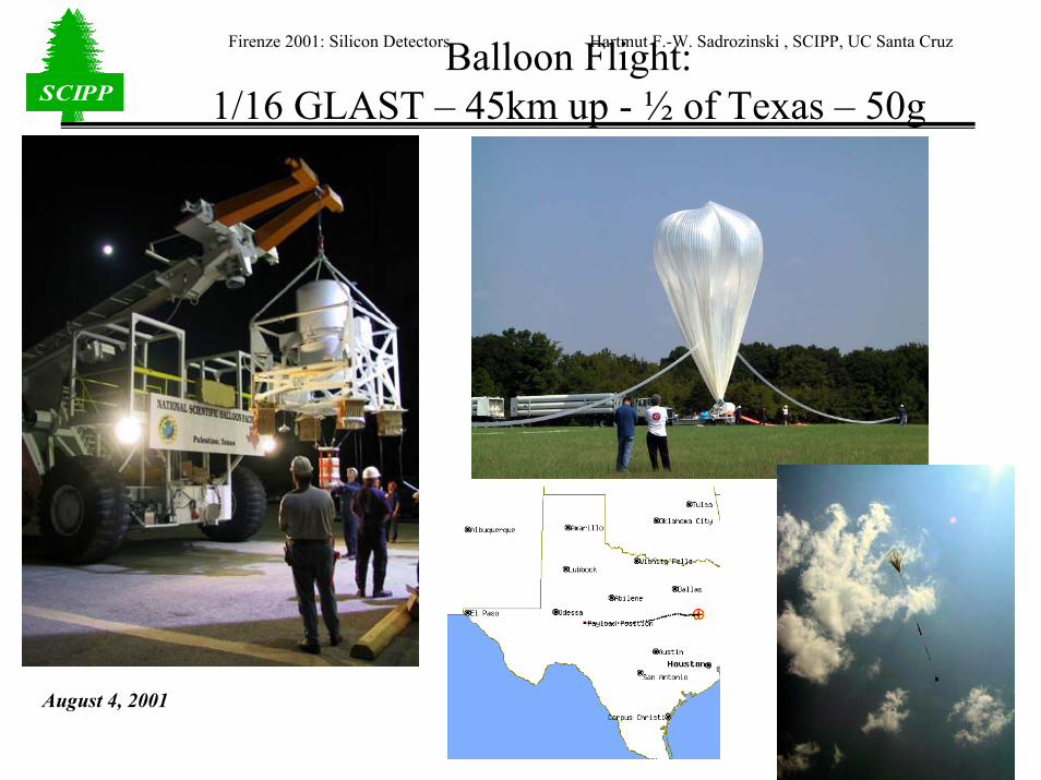
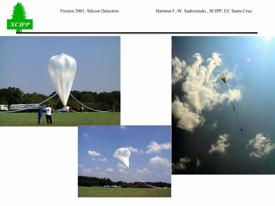
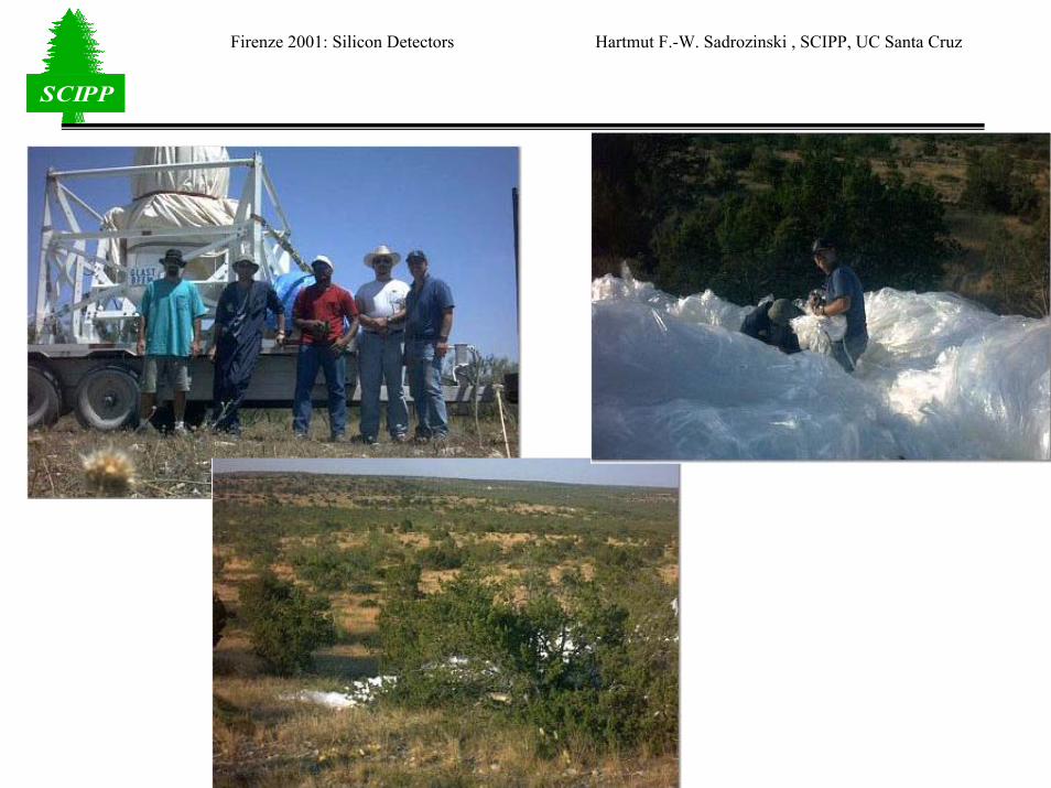
SCIPPSCIPPBalloon Flight:
1/16 GLAST – 45km up - ½ of Texas – 50g
August 4, 2001
Firenze 2001: Silicon Detectors Hartmut F.-W. Sadrozinski , SCIPP, UC Santa Cruz
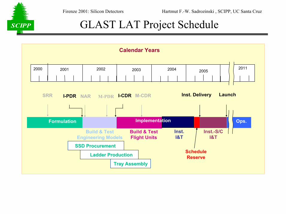
SCIPPSCIPP GLAST LAT Project Schedule
2000 2001 2002 2003 2004 20052011
Formulation Implementation
SRR NAR M-PDR M-CDRI-PDR I-CDR Inst. Delivery Launch
Build & TestEngineering Models
Build & TestFlight Units
Inst.I&T
ScheduleReserve
Inst.-S/CI&T
Ops.
Calendar Years
SSD Procurement SSD Procurement
Ladder Production Ladder Production
Tray AssemblyTray Assembly
Firenze 2001: Silicon Detectors Hartmut F.-W. Sadrozinski , SCIPP, UC Santa Cruz
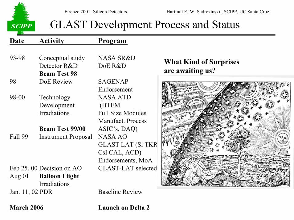
SCIPPSCIPP GLAST Development Process and StatusDate Activity Program
93-98 Conceptual study NASA SR&DDetector R&D DoE R&D Beam Test 98
98 DoE Review SAGENAP Endorsement
98-00 Technology NASA ATDDevelopment (BTEMIrradiations Full Size Modules
Manufact. ProcessBeam Test 99/00 ASIC’s, DAQ)
Fall 99 Instrument Proposal NASA AO GLAST LAT (Si TKR, CsI CAL, ACD)Endorsements, MoA
Feb 25, 00 Decision on AO GLAST-LAT selectedAug 01 Balloon Flight
IrradiationsJan. 11, 02 PDR Baseline Review
March 2006 Launch on Delta 2
What Kind of Surprisesare awaiting us?
Firenze 2001: Silicon Detectors Hartmut F.-W. Sadrozinski , SCIPP, UC Santa Cruz
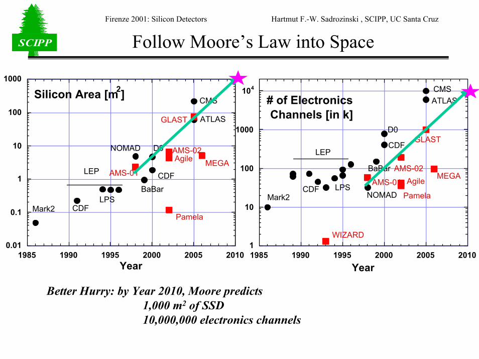
SCIPPSCIPP Follow Moore’s Law into Space
0.01
0.1
1
10
100
1000
1985 1990 1995 2000 2005 2010
Silicon Area [m2]
Year
CDF
ATLASGLAST
CMS
AMS-02
AMS-01
D0
BaBar
NOMAD
LEP
LPSCDFMark2
Pamela
Agile MEGA
1
10
100
1000
104
1985 1990 1995 2000 2005 2010
# of Electronics Channels [in k]
Year
CDF
ATLAS
GLAST
CMS
AMS-02
AMS-01
WIZARD
D0
BaBar
NOMAD
LEP
LPSCDFMark2 Pamela
Agile MEGA
Better Hurry: by Year 2010, Moore predicts 1,000 m2 of SSD10,000,000 electronics channels
Firenze 2001: Silicon Detectors Hartmut F.-W. Sadrozinski , SCIPP, UC Santa Cruz
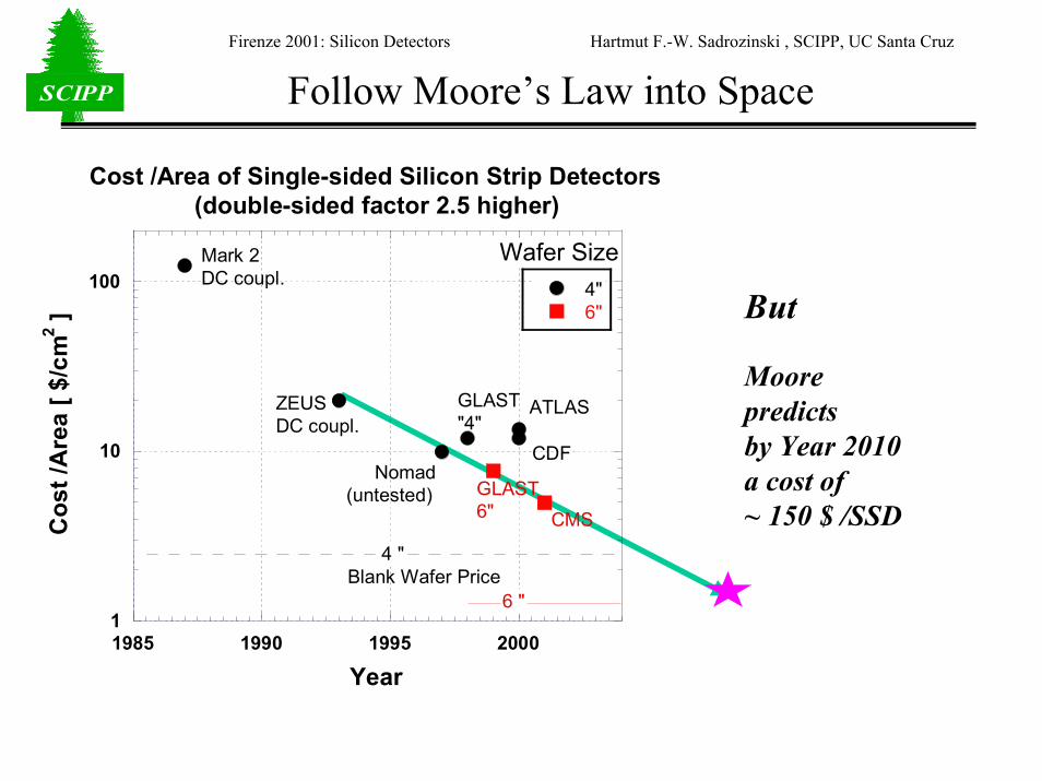
SCIPPSCIPP Follow Moore’s Law into Space
But
Moore predicts by Year 2010 a cost of ~ 150 $ /SSD
1
10
100
1985 1990 1995 2000
Cost /Area of Single-sided Silicon Strip Detectors(double-sided factor 2.5 higher)
4"6"
Cos
t /A
rea
[ $/c
m2 ]
Year
Mark 2DC coupl.
ZEUSDC coupl.
CDFNomad
(untested)
GLAST"4"
ATLAS
GLAST6"
Wafer Size
Blank Wafer Price4 "
6 "
CMS

Firenze 2001: Silicon Detectors Hartmut F.-W. Sadrozinski , SCIPP, UC Santa Cruz
SCIPPSCIPP Challenge #1 : Launch and CTE Mismatch
BTEM TKR tray undergoing random vibration testing at GSFC.
Vibration Testing of a live tray up to 14g.Leakage current before and after shaking identical
Space Qualification:Assembly Methods
MaterialsTests
Aluminum and carbon-fiber mechanical model
of 10 stacked tracker trays, used by Hytec,
Inc. to validate the design in vibration tests.
FEM analysis of (a) TKR tray deflections and (b) of a complete TKR module. Fundamental frequencies are above 550 Hz for the tray and 300 Hz for the module, clamped only at its base.

Firenze 2001: Silicon Detectors Hartmut F.-W. Sadrozinski , SCIPP, UC Santa Cruz
SCIPPSCIPP Challenge #2: On Board Cosmic Ray Rejection
Diffuse High Latitude gamma-ray flux
C.R. Rejection needed 105 : 1 segmented ACD segmented CAL segmented TRK
Radiation Levels: 1krad in a 5year missionIssue: SEE from Heavy Ions (SEU & Latch-up)See below
LVL1 : 5kHzDownlink: 30Hz
Firenze 2001: Silicon Detectors Hartmut F.-W. Sadrozinski , SCIPP, UC Santa Cruz
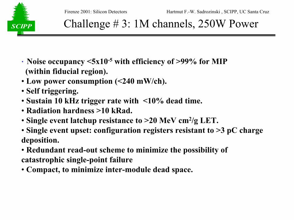
SCIPPSCIPP Challenge # 3: 1M channels, 250W Power
• Noise occupancy <5x10⁻⁵ with efficiency of >99% for MIP (within fiducial region).
• Low power consumption (<240 mW/ch).• Self triggering.• Sustain 10 kHz trigger rate with <10% dead time.• Radiation hardness >10 kRad.• Single event latchup resistance to >20 MeV cm2/g LET.• Single event upset: configuration registers resistant to >3 pC charge deposition.• Redundant read-out scheme to minimize the possibility of catastrophic single-point failure• Compact, to minimize inter-module dead space.
Firenze 2001: Silicon Detectors Hartmut F.-W. Sadrozinski , SCIPP, UC Santa Cruz
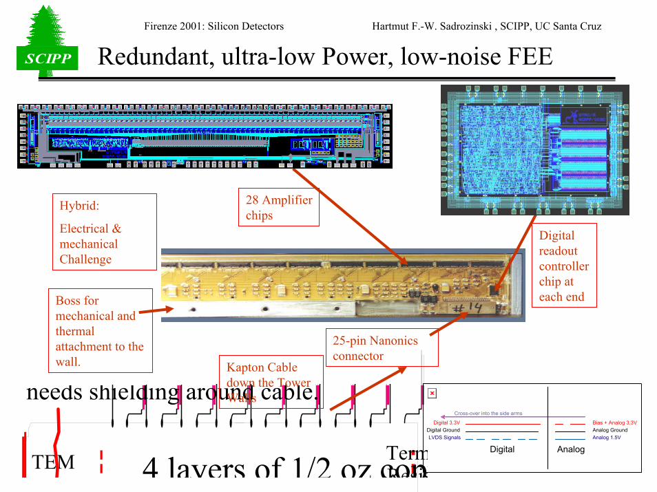
SCIPPSCIPP Redundant, ultra-low Power, low-noise FEE
Boss for mechanical and thermal attachment to the wall.
28 Amplifier chips
TermResis4 layers of 1/2 oz coppTEM
needs shielding around cable.
Digital Analog
Cross-over into the side arms
Bias + Analog 3.3VAnalog GroundAnalog 1.5V
Digital 3.3VDigital GroundLVDS Signals
Kapton Cable down the Tower Walls
Hybrid:
Electrical & mechanical Challenge
Digital readout controller chip at each end
25-pin Nanonics connector
Firenze 2001: Silicon Detectors Hartmut F.-W. Sadrozinski , SCIPP, UC Santa Cruz
SCIPPSCIPP
0 200 400 600 800 1000 1200 1400
10-5
Strip Number
Layer 6x
Occ
upan
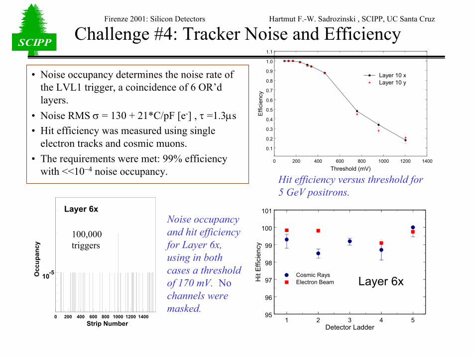
cyChallenge #4: Tracker Noise and Efficiency
• Noise occupancy determines the noise rate of the LVL1 trigger, a coincidence of 6 OR’dlayers.
• Noise RMS σ = 130 + 21*C/pF [e-] , τ =1.3µs• Hit efficiency was measured using single
electron tracks and cosmic muons.• The requirements were met: 99% efficiency
with <<10−4 noise occupancy.0 200 400 600 800 1000 1200 1400
Threshold (mV)
0.1
0.2
0.3
0.4
0.5
0.6
0.7
0.8
0.9
1.0
1.1
Effi
cien
cy
Layer 10 xLayer 10 y
1 2 3 4 5Detector Ladder
95
96
97
98
99
100
101
Hit
Effi
cien
cy
Layer 6xCosmic RaysElectron Beam
Noise occupancy and hit efficiency for Layer 6x, using in both cases a threshold of 170 mV. Nochannels were masked.
Hit efficiency versus threshold for 5 GeV positrons.
100,000 triggers
Firenze 2001: Silicon Detectors Hartmut F.-W. Sadrozinski , SCIPP, UC Santa Cruz
SCIPPSCIPP Challenge #5: Space Environment: RadiationGLAST is in a Low-Earth Orbit (550km):
Shielding of Atmosphere and magnetic Field Avoid (most!) of the radiation belts
Orbit co-determined by Re-entry > 10 Years, < 30years.
USA on ARGOS
Radiation Belts: - High LatitudeSouth Atlantic Anomaly (SAA)-Trapped electrons and protons
responsible for Total Dosecause huge trigger rate(Detectors will be switched off)
Outside radiation Belts:Charged Cosmic Ray Background (p, e, heavy ions) Responsible for Single Event Effects (SEE)
Firenze 2001: Silicon Detectors Hartmut F.-W. Sadrozinski , SCIPP, UC Santa Cruz
SCIPPSCIPP
Long-term Radiation Damage:
Entirely given by electron and proton flux trapped in the SAA
Extremely soft spectrum: Self shielding of Instrument:Blanket, ACD, walls: 2.50g/cm2
Cut-off at 80MeV protons
Radiation: Total Dose & Displacement
0
5
10
15
20
25
30
0 5 10 15 20 25 30
GLAST Silicon Tracker End-of-Mission Signal-to-Noise
S/N E-o-M 1x
S/N E-o-M 5x
Temperature [deg C]
Total Dose 1kRad (5 yrs) -NASA safety factor: 5x-Leakage current increase 50% surface, 50% bulk(same temperature dependence).
Increase in shot noise due to radiation constrains operating temperature to below 25oC.
1
10
100
1000
10000
100000
0.01 0.1 1 10
ElectronsBremsstrahlungProtonsTotal
Full dose - Spherical shield550 km 28° circular orbit
5-year mission - Solar Minimum
Depth (g/cm2 Al)
Firenze 2001: Silicon Detectors Hartmut F.-W. Sadrozinski , SCIPP, UC Santa Cruz
SCIPPSCIPP Heavy Ion Radiation: Temporal Effects (SEE)Linear Energy Transfer LET governs Single Event Effects: SEU, SEL, Punch Through LET is dE/dx: LET (Min ion) ≈ 1.3*10-3 MeV/(mg/cm2), LET ~ Z2 : LET (Fe) ≈ 1-2 MeV/(mg/cm2).
Fe
GLAST IRD
Update from AMS
Firenze 2001: Silicon Detectors Hartmut F.-W. Sadrozinski , SCIPP, UC Santa Cruz
SCIPPSCIPP Challenge # 6: System Reliability
• The LAT Tracker is being designed to operate at its full capability for >5 years.
• There are no consumables in the system, and the solid-state technology is inherently robust and stable.
• Comprehensive radiation testing (SEE and total dose) has been carried out on SSDs and ASICs.
• Long-term environmental testing is in progress for the SSDs.• A preliminary reliability analysis has been made of the electronics
readout system: LAT-TD-00178.– The mean time to failure is conservatively estimated to be 2.5
years.– The vast majority of failures considered here would have little or
no effect on the Tracker performance.– Modularity and redundancy in the system limit the impact of more
serious failures.– Modularity and redundancy in the system allow finite number of
failures without loss of performance
Firenze 2001: Silicon Detectors Hartmut F.-W. Sadrozinski , SCIPP, UC Santa Cruz
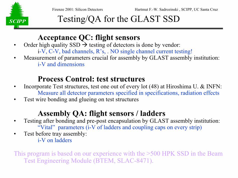
SCIPPSCIPP Testing/QA for the GLAST SSD
Acceptance QC: flight sensors• Order high quality SSD testing of detectors is done by vendor:
i-V, C-V, bad channels, R’s, . NO single channel current testing!• Measurement of parameters crucial for assembly by GLAST assembly institution:
i-V and dimensions
Process Control: test structures• Incorporate Test structures, test one out of every lot (48) at Hiroshima U. & INFN:
Measure all detector parameters specified in specifications, radiation effects• Test wire bonding and glueing on test structures
Assembly QA: flight sensors / ladders• Testing after bonding and pre-post encapsulation by GLAST assembly institution:
“Vital” parameters (i-V of ladders and coupling caps on every strip)• Test before tray assembly:
i-V on ladders
This program is based on our experience with the >500 HPK SSD in the Beam Test Engineering Module (BTEM, SLAC-8471).
Firenze 2001: Silicon Detectors Hartmut F.-W. Sadrozinski , SCIPP, UC Santa Cruz
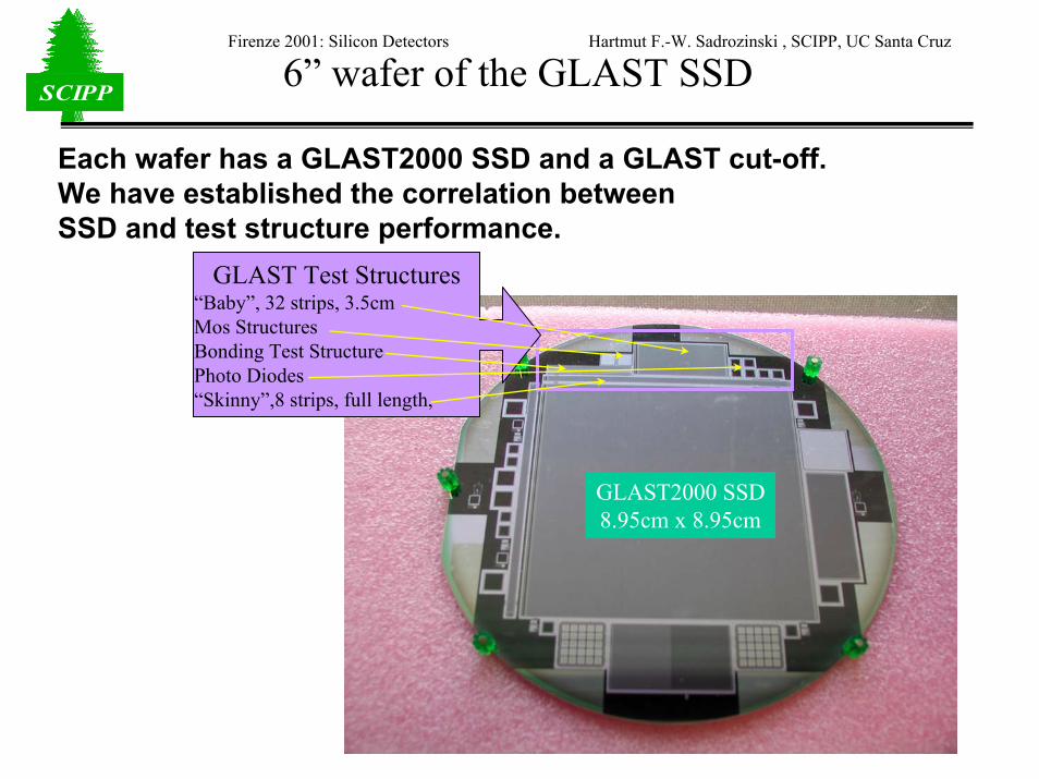
SCIPPSCIPP 6” wafer of the GLAST SSD
Each wafer has a GLAST2000 SSD and a GLAST cut-off.We have established the correlation between SSD and test structure performance.
GLAST Test Structures“Baby”, 32 strips, 3.5cmMos Structures Bonding Test StructurePhoto Diodes“Skinny”,8 strips, full length,
GLAST2000 SSD8.95cm x 8.95cm

Firenze 2001: Silicon Detectors Hartmut F.-W. Sadrozinski , SCIPP, UC Santa Cruz
SCIPPSCIPP Test Structures on the GLAST SSD Wafer
“Skinny”, 8 strips, full length
Cint, Rint, RAl,
Bonding Test Structure
MOS Structures
“Baby”, 32 strips, 3.5cm long
I-V (10kRad), Vdep,
Fiducials:AlignmentBonding

Firenze 2001: Silicon Detectors Hartmut F.-W. Sadrozinski , SCIPP, UC Santa Cruz
SCIPPSCIPP Ladder assembly (INFN Pisa)
GlueingAlignment
Service box for bondingTransfer bridge
Firenze 2001: Silicon Detectors Hartmut F.-W. Sadrozinski , SCIPP, UC Santa Cruz
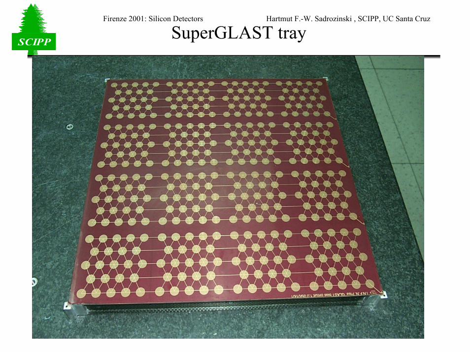
SCIPPSCIPPSuperGLAST tray

Firenze 2001: Silicon Detectors Hartmut F.-W. Sadrozinski , SCIPP, UC Santa Cruz
SCIPPSCIPP Placement of ladders on trays – 1st exercise
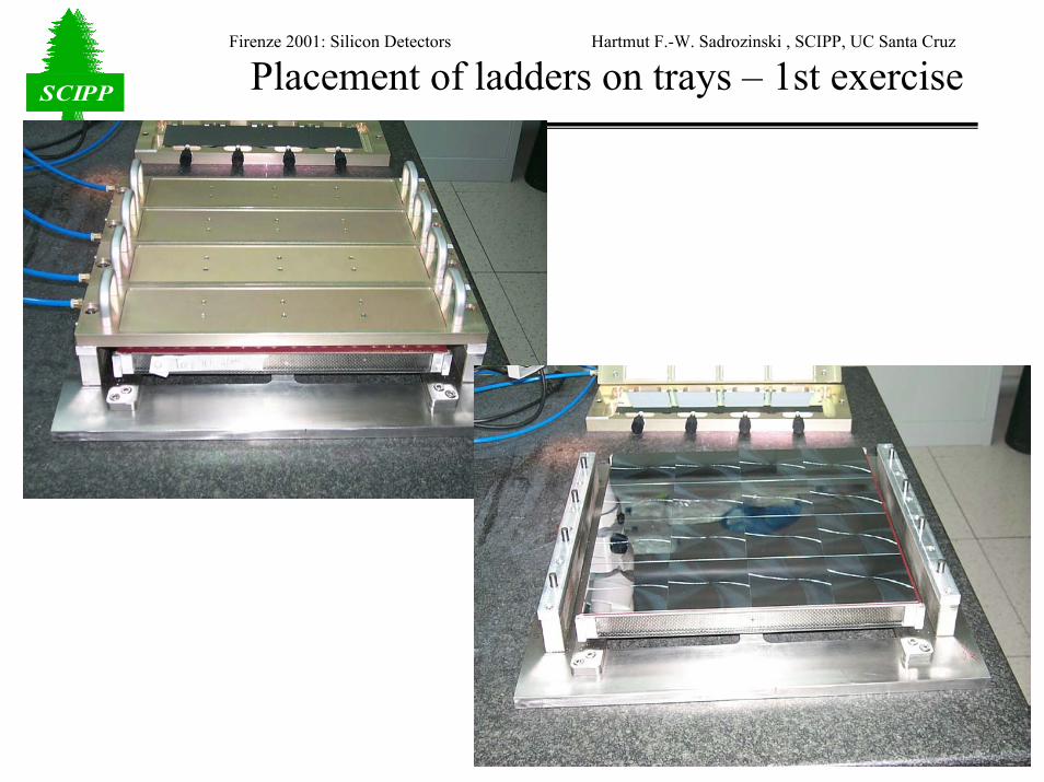
Firenze 2001: Silicon Detectors Hartmut F.-W. Sadrozinski , SCIPP, UC Santa Cruz
SCIPPSCIPP Placement of ladders on trays – 1st exercise
Firenze 2001: Silicon Detectors Hartmut F.-W. Sadrozinski , SCIPP, UC Santa Cruz
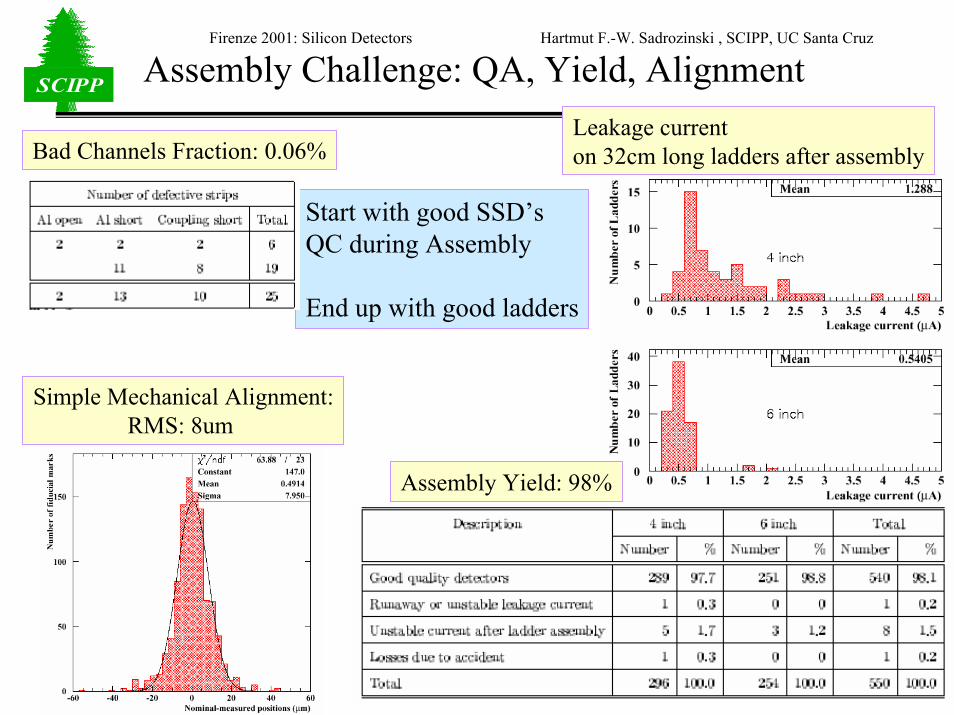
SCIPPSCIPP Assembly Challenge: QA, Yield, AlignmentLeakage current on 32cm long ladders after assembly
Assembly Yield: 98%
Bad Channels Fraction: 0.06%
Start with good SSD’sQC during Assembly
End up with good ladders
Simple Mechanical Alignment:RMS: 8um
Firenze 2001: Silicon Detectors Hartmut F.-W. Sadrozinski , SCIPP, UC Santa Cruz
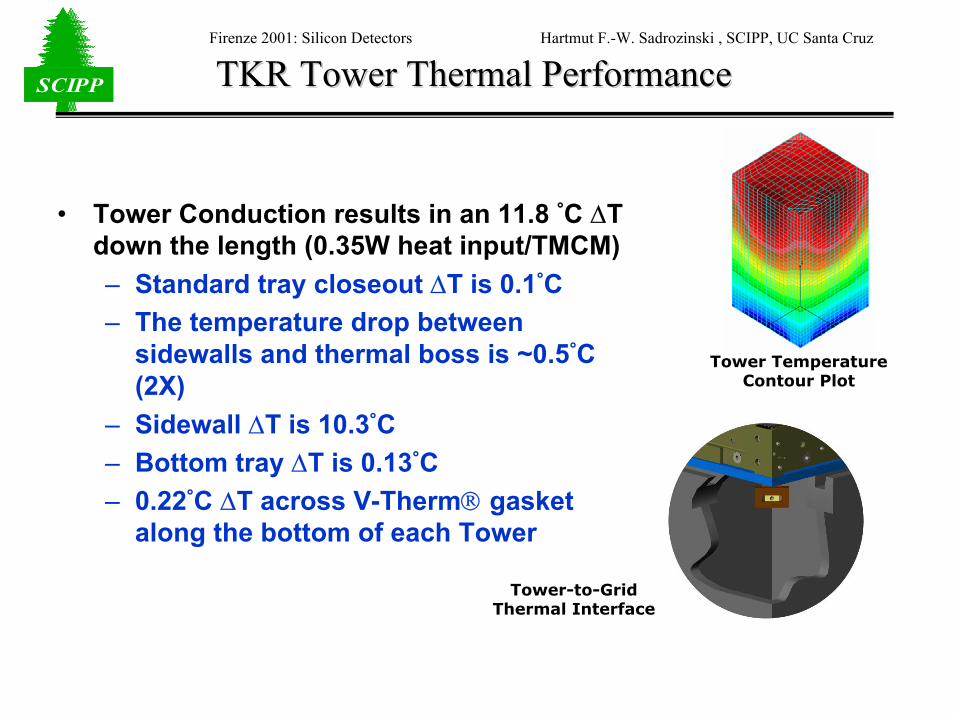
SCIPPSCIPP TKR Tower Thermal PerformanceTKR Tower Thermal Performance
• Tower Conduction results in an 11.8 °C ∆T down the length (0.35W heat input/TMCM)– Standard tray closeout ∆T is 0.1°C – The temperature drop between
sidewalls and thermal boss is ~0.5°C (2X)
– Sidewall ∆T is 10.3°C– Bottom tray ∆T is 0.13°C – 0.22°C ∆T across V-Therm gasket
along the bottom of each Tower
Tower Temperature Contour Plot
Tower-to-Grid Thermal Interface
Firenze 2001: Silicon Detectors Hartmut F.-W. Sadrozinski , SCIPP, UC Santa Cruz
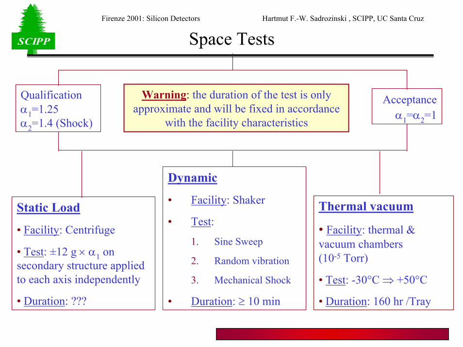
SCIPPSCIPP Space Tests
Thermal vacuum
• Facility: thermal & vacuum chambers (10-5 Torr)
• Test: -30°C ⇒ +50°C
• Duration: 160 hr /Tray
Acceptanceα1=α2=1
Qualificationα1=1.25α2=1.4 (Shock)
Dynamic
• Facility: Shaker
• Test:
1. Sine Sweep
2. Random vibration
3. Mechanical Shock
• Duration: ≥ 10 min
Static Load
• Facility: Centrifuge
• Test: ±12 g × α1 on secondary structure applied to each axis independently
• Duration: ???
Warning: the duration of the test is only approximate and will be fixed in accordance
with the facility characteristics

Firenze 2001: Silicon Detectors Hartmut F.-W. Sadrozinski , SCIPP, UC Santa Cruz
SCIPPSCIPP Space tests: Trays
dynamic (sine sweep/random vibration)Qualification (USA)
thermal
dynamic (random vibration):• fixture (4.6Mlt. + VAT)• test:1) lab use for 1.5 days (shaker) (2.8Mlt. + VAT)2) data acquisition and reporting (1.474Mlt. + VAT)3) leakage current measurement:2 hrs/tray (400klt. + VAT), 380 trays
Acceptance (Italy)
thermal
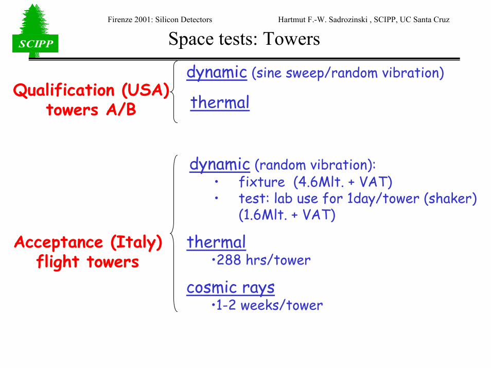
Firenze 2001: Silicon Detectors Hartmut F.-W. Sadrozinski , SCIPP, UC Santa Cruz
SCIPPSCIPP Space tests: Towers
dynamic (sine sweep/random vibration)Qualification (USA)
towers A/B thermal
thermal•288 hrs/tower
cosmic rays•1-2 weeks/tower
dynamic (random vibration):• fixture (4.6Mlt. + VAT)• test: lab use for 1day/tower (shaker)
(1.6Mlt. + VAT)
Acceptance (Italy)flight towers

Firenze 2001: Silicon Detectors Hartmut F.-W. Sadrozinski , SCIPP, UC Santa Cruz
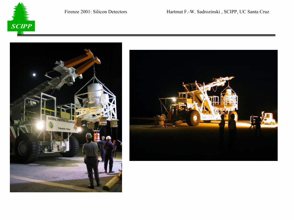
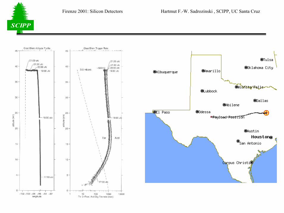
SCIPPSCIPP GLAST LAT Balloon Flight
Firenze 2001: Silicon Detectors Hartmut F.-W. Sadrozinski , SCIPP, UC Santa Cruz
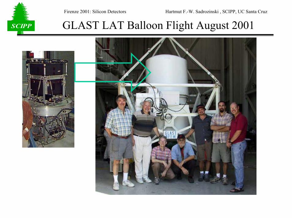
SCIPPSCIPP GLAST LAT Balloon Flight August 2001
Firenze 2001: Silicon Detectors Hartmut F.-W. Sadrozinski , SCIPP, UC Santa Cruz
SCIPPSCIPP
Firenze 2001: Silicon Detectors Hartmut F.-W. Sadrozinski , SCIPP, UC Santa Cruz
SCIPPSCIPP
Firenze 2001: Silicon Detectors Hartmut F.-W. Sadrozinski , SCIPP, UC Santa Cruz
SCIPPSCIPP
Firenze 2001: Silicon Detectors Hartmut F.-W. Sadrozinski , SCIPP, UC Santa Cruz
SCIPPSCIPP
Firenze 2001: Silicon Detectors Hartmut F.-W. Sadrozinski , SCIPP, UC Santa Cruz
SCIPPSCIPP
Firenze 2001: Silicon Detectors Hartmut F.-W. Sadrozinski , SCIPP, UC Santa Cruz
SCIPPSCIPPThe LAT Hardware
Firenze 2001: Silicon Detectors Hartmut F.-W. Sadrozinski , SCIPP, UC Santa Cruz
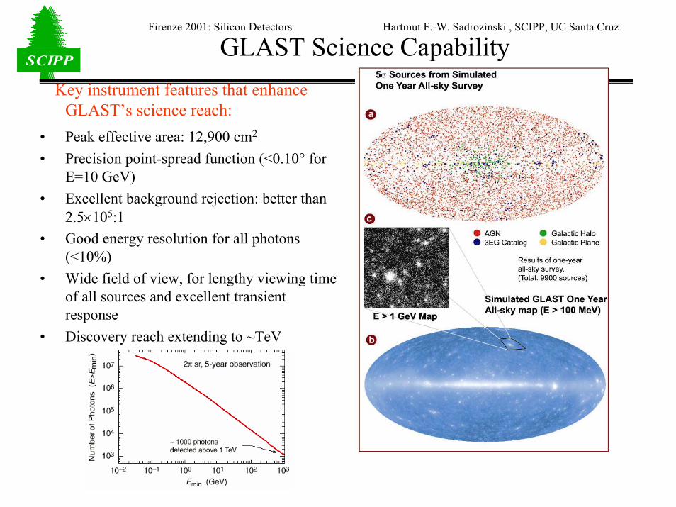
SCIPPSCIPPGLAST Science Capability
Key instrument features that enhanceGLAST’s science reach:
• Peak effective area: 12,900 cm2
• Precision point-spread function (<0.10° for E=10 GeV)
• Excellent background rejection: better than 2.5×10⁵:1
• Good energy resolution for all photons (<10%)
• Wide field of view, for lengthy viewing time of all sources and excellent transient response
• Discovery reach extending to ~TeV

Firenze 2001: Silicon Detectors Hartmut F.-W. Sadrozinski , SCIPP, UC Santa Cruz
SCIPPSCIPP Science Capabilities - Sensitivity
200 γ bursts per year prompt emission sampled to > 20 µs
AGN flares > 2 mntime profile +∆E/E ⇒ physics of jets and acceleration
γ bursts delayed emission
all 3EG sources + 80 new in 2 days
⇒ periodicity searches (pulsars & X-ray binaries)⇒ pulsar beam & emission vs. luminosity, age, B
104 sources in 1-yr survey⇒ AGN: logN-logS, duty cycle,
emission vs. type, redshift, aspect angle⇒ extragalactic background light (γ + IR-opt)⇒ new γ sources (µQSO, external galaxies, clusters)
1 yr
100 s
1 orbit
1 day
3EG limit
0.01
0.001
LAT 1 yr2.3 10-9
cm-2s-1
large field-of-view

Firenze 2001: Silicon Detectors Hartmut F.-W. Sadrozinski , SCIPP, UC Santa Cruz
SCIPPSCIPP Science: High-Energy Behavior of GRBs
Important GLAST properties for achieving science objectives:
• Large area• Low instrument deadtime (20 µs)• Energy range to >300 GeV• Large FOV
Expected Numbers of GRBs and Delayed Emission in GLAST
GLAST will probe the time structure of GRB’s to the µs time scaleSpectral and temporal information might allow observation of quantum gravity effects.
Time between detection of photons
Firenze 2001: Silicon Detectors Hartmut F.-W. Sadrozinski , SCIPP, UC Santa Cruz
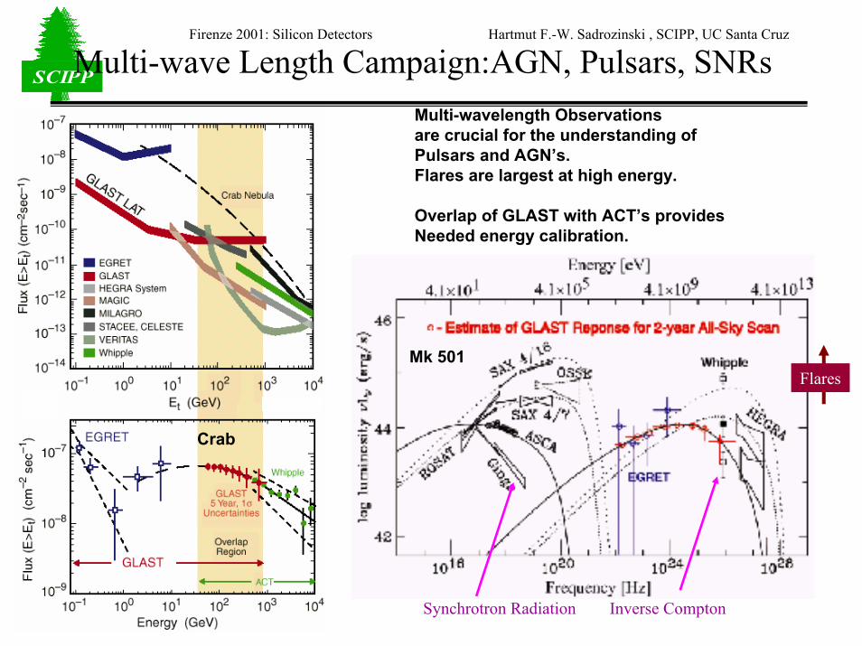
SCIPPSCIPPMulti-wave Length Campaign:AGN, Pulsars, SNRsMulti-wavelength Observations are crucial for the understanding of Pulsars and AGN’s. Flares are largest at high energy.
Overlap of GLAST with ACT’s provides Needed energy calibration.
Crab
Mk 501
Synchrotron Radiation Inverse Compton
Flares
Firenze 2001: Silicon Detectors Hartmut F.-W. Sadrozinski , SCIPP, UC Santa Cruz
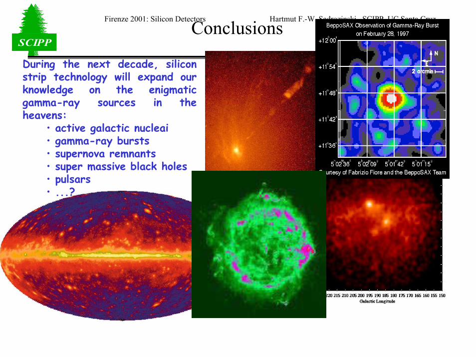
SCIPPSCIPPConclusions
During the next decade, silicon strip technology will expand our knowledge on the enigmatic gamma-ray sources in the heavens:
• active galactic nucleai• gamma-ray bursts• supernova remnants• super massive black holes• pulsars• ...?
Firenze 2001: Silicon Detectors Hartmut F.-W. Sadrozinski , SCIPP, UC Santa Cruz
SCIPPSCIPP Back-up
Firenze 2001: Silicon Detectors Hartmut F.-W. Sadrozinski , SCIPP, UC Santa Cruz
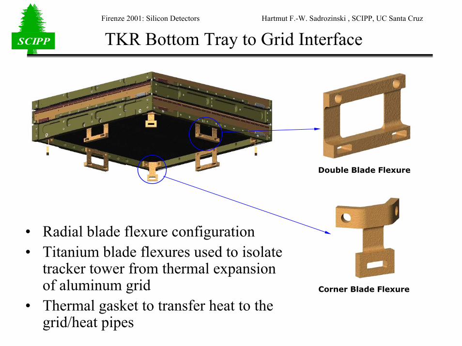
SCIPPSCIPP TKR Bottom Tray to Grid Interface
• Radial blade flexure configuration• Titanium blade flexures used to isolate
tracker tower from thermal expansion of aluminum grid
• Thermal gasket to transfer heat to the grid/heat pipes
Corner Blade Flexure
Double Blade Flexure
Firenze 2001: Silicon Detectors Hartmut F.-W. Sadrozinski , SCIPP, UC Santa Cruz
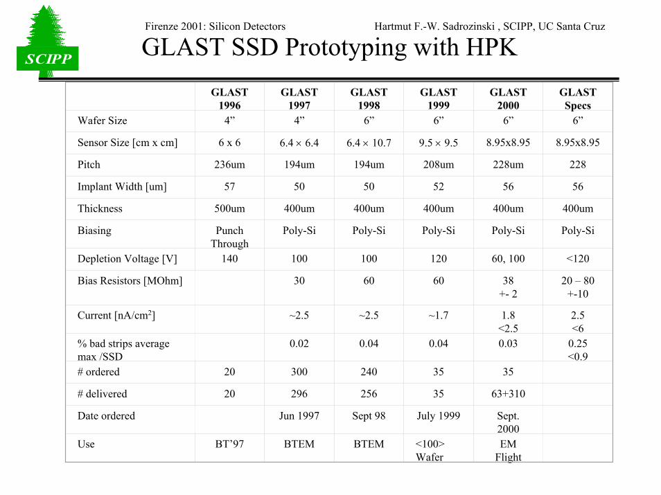
SCIPPSCIPP GLAST SSD Prototyping with HPKGLAST
1996GLAST
1997GLAST
1998GLAST
1999 GLAST
2000GLAST Specs
Wafer Size 4” 4” 6” 6” 6” 6”
Sensor Size [cm x cm] 6 x 6 6.4 × 6.4 6.4 × 10.7 9.5 × 9.5 8.95x8.95 8.95x8.95
Pitch 236um 194um 194um 208um 228um 228
Implant Width [um] 57 50 50 52 56 56
Thickness 500um 400um 400um 400um 400um 400um
Biasing Punch Through
Poly-Si Poly-Si Poly-Si Poly-Si Poly-Si
Depletion Voltage [V] 140 100 100 120 60, 100 <120
Bias Resistors [MOhm] 30 60 60 38+- 2
20 – 80+-10
Current [nA/cm2] ~2.5 ~2.5 ~1.7 1.8<2.5
2.5<6
% bad strips averagemax /SSD
0.02 0.04 0.04 0.03 0.25 <0.9
# ordered 20 300 240 35 35
# delivered 20 296 256 35 63+310
Date ordered Jun 1997 Sept 98 July 1999 Sept. 2000
Use BT’97 BTEM BTEM <100> Wafer
EMFlight
Firenze 2001: Silicon Detectors Hartmut F.-W. Sadrozinski , SCIPP, UC Santa Cruz
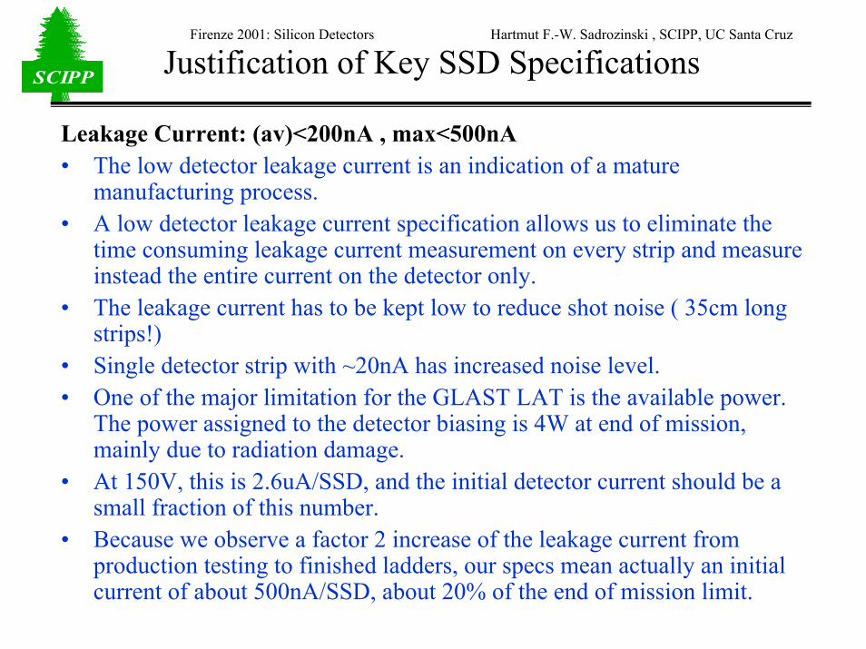
SCIPPSCIPP Justification of Key SSD Specifications
Leakage Current: (av)<200nA , max<500nA• The low detector leakage current is an indication of a mature
manufacturing process. • A low detector leakage current specification allows us to eliminate the
time consuming leakage current measurement on every strip and measure instead the entire current on the detector only.
• The leakage current has to be kept low to reduce shot noise ( 35cm long strips!)
• Single detector strip with ~20nA has increased noise level.• One of the major limitation for the GLAST LAT is the available power.
The power assigned to the detector biasing is 4W at end of mission, mainly due to radiation damage.
• At 150V, this is 2.6uA/SSD, and the initial detector current should be a small fraction of this number.
• Because we observe a factor 2 increase of the leakage current from production testing to finished ladders, our specs mean actually an initial current of about 500nA/SSD, about 20% of the end of mission limit.
Firenze 2001: Silicon Detectors Hartmut F.-W. Sadrozinski , SCIPP, UC Santa Cruz
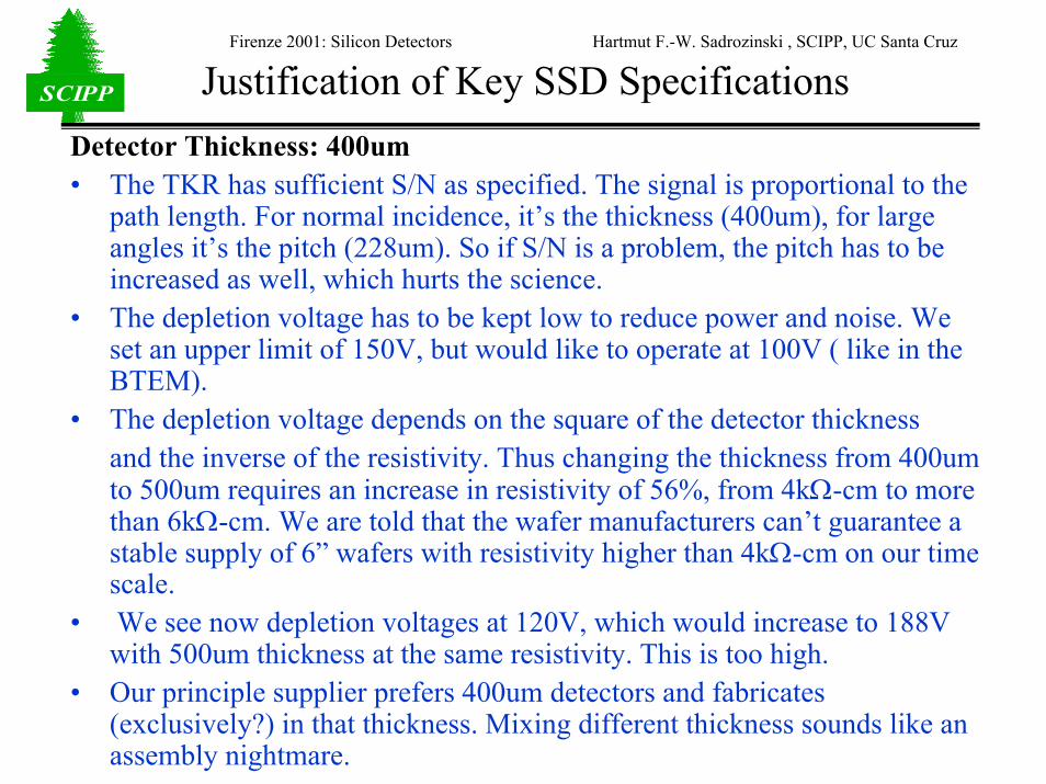
SCIPPSCIPP Justification of Key SSD SpecificationsDetector Thickness: 400um• The TKR has sufficient S/N as specified. The signal is proportional to the
path length. For normal incidence, it’s the thickness (400um), for large angles it’s the pitch (228um). So if S/N is a problem, the pitch has to be increased as well, which hurts the science.
• The depletion voltage has to be kept low to reduce power and noise. We set an upper limit of 150V, but would like to operate at 100V ( like in the BTEM).
• The depletion voltage depends on the square of the detector thicknessand the inverse of the resistivity. Thus changing the thickness from 400um to 500um requires an increase in resistivity of 56%, from 4kΩ-cm to more than 6kΩ-cm. We are told that the wafer manufacturers can’t guarantee a stable supply of 6” wafers with resistivity higher than 4kΩ-cm on our time scale.
• We see now depletion voltages at 120V, which would increase to 188V with 500um thickness at the same resistivity. This is too high.
• Our principle supplier prefers 400um detectors and fabricates (exclusively?) in that thickness. Mixing different thickness sounds like an assembly nightmare.
Firenze 2001: Silicon Detectors Hartmut F.-W. Sadrozinski , SCIPP, UC Santa Cruz
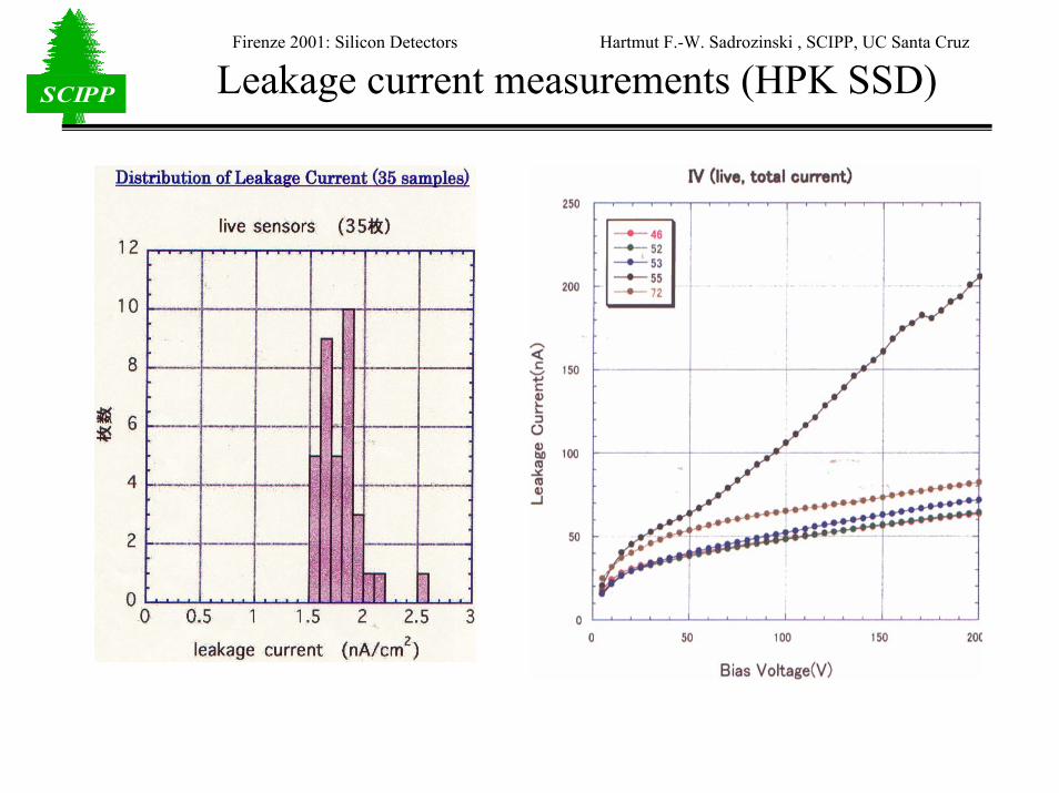
SCIPPSCIPP Leakage current measurements (HPK SSD)
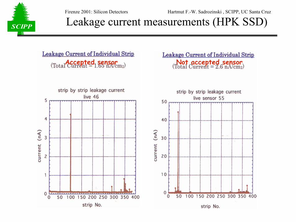
Firenze 2001: Silicon Detectors Hartmut F.-W. Sadrozinski , SCIPP, UC Santa Cruz
SCIPPSCIPP Leakage current measurements (HPK SSD)
Accepted sensor Not accepted sensor

Firenze 2001: Silicon Detectors Hartmut F.-W. Sadrozinski , SCIPP, UC Santa Cruz
SCIPPSCIPP TKR Tray Sandwich Structure
• Lightweight 4 piece machined closeout frame, bonded to face sheets and core to form a sandwich structure
Gr/CE Face Sheet
MCM Closeout Wall
Thermal Boss
Aluminum Honeycomb Core
Structural Closeout Wall
Firenze 2001: Silicon Detectors Hartmut F.-W. Sadrozinski , SCIPP, UC Santa Cruz
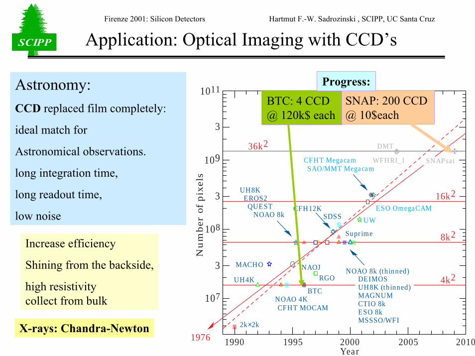
SCIPPSCIPP Application: Optical Imaging with CCD’s
36k2
16k2
8k2
4k2
2000Year
20051990 1995 2010
2k×2k
MACHO
Suprime
UH4K
NOAO 4KCFHT MOCAM
NAOJ
BTC
RGO
UH8K EROS2 QUEST NOAO 8k
UW
DMT
WFHRI_1
SDSSCFH12K ESO OmegaCAM
NOAO 8k (thinned)3
3
3
107
108
109
1011
Nu
mber
of
pix
els
DEIMOSUH8K (thinned)MAGNUMCTIO 8kESO 8kMSSSO/WFI
CFHT MegacamSAO/MMT Megacam
1976
SNAPsat
SNAP: 200 CCD @ 10$each
BTC: 4 CCD @ 120k$ each
Progress:Astronomy: CCD replaced film completely:
ideal match for
Astronomical observations.
long integration time,
long readout time,
low noise
Increase efficiency
Shining from the backside,
high resistivitycollect from bulk
X-rays: Chandra-Newton
Firenze 2001: Silicon Detectors Hartmut F.-W. Sadrozinski , SCIPP, UC Santa Cruz
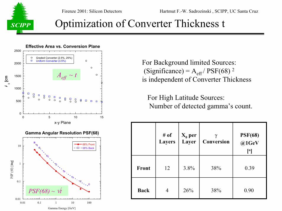
SCIPPSCIPP Optimization of Converter Thickness t
0
500
1000
1500
2000
2500
0 5 10 15
Effective Area vs. Conversion Plane
Graded Converter (2.5%, 25%)Uniform Converter (3.5%)
x-y Plane
0.01
0.1
1
10
0.01 0.1 1 10 100
Gamma Angular Resolution PSF(68)
68% Front68% Back
Gamma Energy [GeV]
Aeff ~ t
PSF(68) ~ √t
For Background limited Sources:(Significance) = Aeff / PSF(68) 2
is independent of Converter Thickness
For High Latitude Sources:Number of detected gamma’s count.
0.9038%26%4Back
0.3938%3.8%12Front
PSF(68)@1GeV
[o]
γConversion
X0 per Layer
# of Layers
Firenze 2001: Silicon Detectors Hartmut F.-W. Sadrozinski , SCIPP, UC Santa Cruz
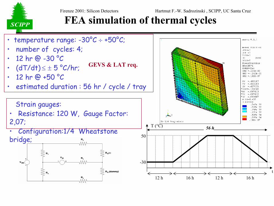
SCIPPSCIPP FEA simulation of thermal cycles
• temperature range: -30°C ÷ +50°C;• number of cycles: 4;• 12 hr @ -30 °C• (dT/dt) ≤ ± 5 °C/hr;• 12 hr @ +50 °C• estimated duration : 56 hr / cycle / tray
GEVS & LAT req.
Strain gauges:• Resistance: 120 W, Gauge Factor: 2,07;• Configuration:1/4 Wheatstonebridge;
t
-30
50
56 h
12 h 12 h16 h 16 h
T (°C)
Firenze 2001: Silicon Detectors Hartmut F.-W. Sadrozinski , SCIPP, UC Santa Cruz
SCIPPSCIPP Strain during thermal cycles

Firenze 2001: Silicon Detectors Hartmut F.-W. Sadrozinski , SCIPP, UC Santa Cruz
SCIPPSCIPP
Controlaccelerometer
Random vibration (independently on x,y,z):• Range: 20 ÷ 2000 Hz• Notching at normal modes frequencies• Duration: few minutes
• Normal modes search (>500Hz);• Range: 10 ÷ 2000 Hz;• Amplitude: 0.25 g ÷ 0.5g;• Frequency scan velocity: 2 ÷ 4 oct / min; • Test duration : ~ 1 min.
Sine sweep (independently on x,y,z):
FEA simulation of vibrational cycles
max (Uz)rms 160µm(at tray centre)
max (σeq)rms 4MPa(at tray centre)
Firenze 2001: Silicon Detectors Hartmut F.-W. Sadrozinski , SCIPP, UC Santa Cruz
SCIPPSCIPP Application: Compton Telescope
Compton effect: 2-body reaction correlates energy transfer with scattering angle
−−=
12
2 111cosEE
cmeϕPrecise Energy measurement of Compton electrons constrains the scattering angle.
T. Kamae: Multiple Compton scattersallow good determination of the incident angle, and energy
Thick Silicon detectors increase the conversion probability and energy resolution