
S1D15000 Series Technical Manual - Kyocera...S1D15605 Series 8–2 EPSON Rev. 2.4a Series...
89
Rev.2.4a S1D15605 Series Technical Manual
Transcript of S1D15000 Series Technical Manual - Kyocera...S1D15605 Series 8–2 EPSON Rev. 2.4a Series...

Rev.2.4a
S1D15605 Series Technical Manual
NOTICE No part of this material may be reproduced or duplicated in any form or by any means without the written permission of Seiko Epson. Seiko Epson reserves the right to make changes to this material without notice. Seiko Epson does not assume any liability of any kind arising out of any inaccuracies contained in this material or due to its application or use in any product or circuit and, further, there is no representation that this material is applicable to products requiring high level reliability, such as, medical products. Moreover, no license to any intellectual property rights is granted by implication or otherwise, and there is no representation or warranty that anything made in accordance with this material will be free from any patent or copyright infringement of a third party. This material or portions thereof may contain technology or the subject relating to strategic products under the control of the Foreign Exchange and Foreign Trade Law of Japan and may require an export license from the Ministry of International Trade and Industry or other approval from another government agency. All other product names mentioned herein are trademarks and/or registered trademarks of their respective companies.
©SEIKO EPSON CORPORATION 2005, All rights reserved.

– i –
Contents
1. DESCRIPTION ................................................................................................................................................ 8-1
2. FEATURES...................................................................................................................................................... 8-1
3. BLOCK DIAGRAM ........................................................................................................................................... 8-3
4. PAD ................................................................................................................................................................. 8-4
5. PIN DESCRIPTIONS .....................................................................................................................................8-20
6. DESCRIPTION OF FUNCTIONS ..................................................................................................................8-24
7. COMMANDS .................................................................................................................................................8-49
8. COMMAND DESCRIPTION ..........................................................................................................................8-58
9. ABSOLUTE MAXIMUM RATINGS ................................................................................................................8-64
10. DC CHARACTERISTICS ...............................................................................................................................8-65
11. TIMING CHARACTERISTICS .......................................................................................................................8-73
12. THE MPU INTERFACE (REFERENCE EXAMPLES) ...................................................................................8-81
13. CONNECTIONS BETWEEN LCD DRIVERS (REFERENCE EXAMPLE) .....................................................8-82
14. CONNECTIONS BETWEEN LCD DRIVERS (REFERENCE EXAMPLES) ..................................................8-83
15. A SAMPLE TCP PIN ASSIGNMENT .............................................................................................................8-84
16. EXTERNAL VIEW OF TCP PINS ..................................................................................................................8-85
Rev. 2.4a
S1D15605 Series
Rev. 2.4a EPSON 8–1
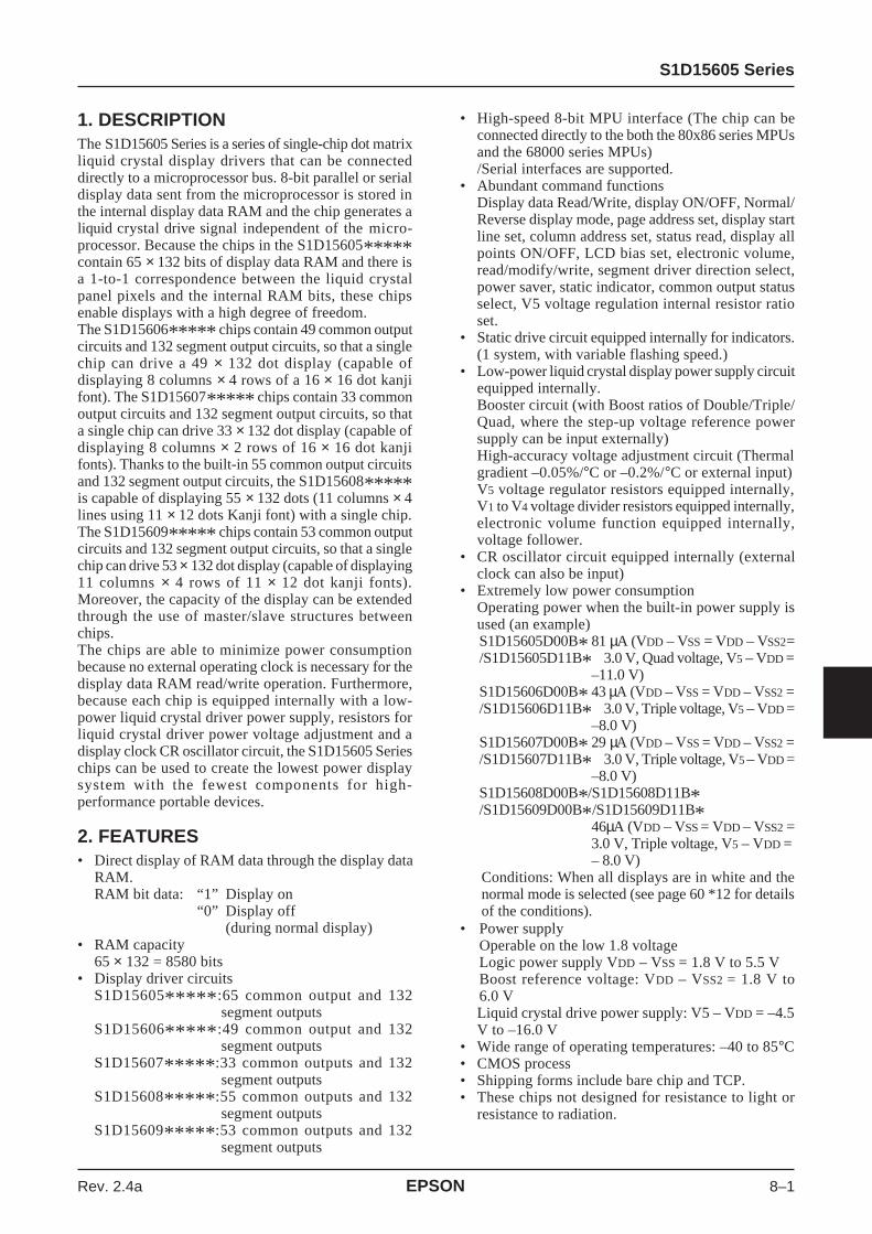
1. DESCRIPTIONThe S1D15605 Series is a series of single-chip dot matrixliquid crystal display drivers that can be connecteddirectly to a microprocessor bus. 8-bit parallel or serialdisplay data sent from the microprocessor is stored inthe internal display data RAM and the chip generates aliquid crystal drive signal independent of the micro-processor. Because the chips in the S1D15605*****contain 65 × 132 bits of display data RAM and there isa 1-to-1 correspondence between the liquid crystalpanel pixels and the internal RAM bits, these chipsenable displays with a high degree of freedom.The S1D15606***** chips contain 49 common outputcircuits and 132 segment output circuits, so that a singlechip can drive a 49 × 132 dot display (capable ofdisplaying 8 columns × 4 rows of a 16 × 16 dot kanjifont). The S1D15607***** chips contain 33 commonoutput circuits and 132 segment output circuits, so thata single chip can drive 33 × 132 dot display (capable ofdisplaying 8 columns × 2 rows of 16 × 16 dot kanjifonts). Thanks to the built-in 55 common output circuitsand 132 segment output circuits, the S1D15608*****is capable of displaying 55 × 132 dots (11 columns × 4lines using 11 × 12 dots Kanji font) with a single chip.The S1D15609***** chips contain 53 common outputcircuits and 132 segment output circuits, so that a singlechip can drive 53 × 132 dot display (capable of displaying11 columns × 4 rows of 11 × 12 dot kanji fonts).Moreover, the capacity of the display can be extendedthrough the use of master/slave structures betweenchips.The chips are able to minimize power consumptionbecause no external operating clock is necessary for thedisplay data RAM read/write operation. Furthermore,because each chip is equipped internally with a low-power liquid crystal driver power supply, resistors forliquid crystal driver power voltage adjustment and adisplay clock CR oscillator circuit, the S1D15605 Serieschips can be used to create the lowest power displaysystem with the fewest components for high-performance portable devices.
2. FEATURES• Direct display of RAM data through the display data
RAM.RAM bit data: “1” Display on
“0” Display off(during normal display)
• RAM capacity65 × 132 = 8580 bits
• Display driver circuitsS1D15605***** :65 common output and 132
segment outputsS1D15606***** :49 common output and 132
segment outputsS1D15607***** :33 common outputs and 132
segment outputsS1D15608***** :55 common outputs and 132
segment outputsS1D15609***** :53 common outputs and 132
segment outputs
• High-speed 8-bit MPU interface (The chip can beconnected directly to the both the 80x86 series MPUsand the 68000 series MPUs)/Serial interfaces are supported.
• Abundant command functionsDisplay data Read/Write, display ON/OFF, Normal/Reverse display mode, page address set, display startline set, column address set, status read, display allpoints ON/OFF, LCD bias set, electronic volume,read/modify/write, segment driver direction select,power saver, static indicator, common output statusselect, V5 voltage regulation internal resistor ratioset.
• Static drive circuit equipped internally for indicators.(1 system, with variable flashing speed.)
• Low-power liquid crystal display power supply circuitequipped internally.Booster circuit (with Boost ratios of Double/Triple/Quad, where the step-up voltage reference powersupply can be input externally)High-accuracy voltage adjustment circuit (Thermalgradient –0.05%/°C or –0.2%/°C or external input)V5 voltage regulator resistors equipped internally,V1 to V4 voltage divider resistors equipped internally,electronic volume function equipped internally,voltage follower.
• CR oscillator circuit equipped internally (externalclock can also be input)
• Extremely low power consumptionOperating power when the built-in power supply isused (an example)S1D15605D00B* 81 µA (VDD – VSS = VDD – VSS2=/S1D15605D11B* 3.0 V, Quad voltage, V5 – VDD =
–11.0 V)S1D15606D00B* 43 µA (VDD – VSS = VDD – VSS2 =/S1D15606D11B* 3.0 V, Triple voltage, V5 – VDD =
–8.0 V)S1D15607D00B* 29 µA (VDD – VSS = VDD – VSS2 =/S1D15607D11B* 3.0 V, Triple voltage, V5 – VDD =
–8.0 V)S1D15608D00B*/S1D15608D11B*/S1D15609D00B* /S1D15609D11B*
46µA (VDD – VSS = VDD – VSS2 =3.0 V, Triple voltage, V5 – VDD =– 8.0 V)
Conditions: When all displays are in white and thenormal mode is selected (see page 60 *12 for detailsof the conditions).
• Power supplyOperable on the low 1.8 voltageLogic power supply VDD – VSS = 1.8 V to 5.5 VBoost reference voltage: VDD – VSS2 = 1.8 V to6.0 VLiquid crystal drive power supply: V5 – VDD = –4.5V to –16.0 V
• Wide range of operating temperatures: –40 to 85°C• CMOS process• Shipping forms include bare chip and TCP.• These chips not designed for resistance to light or
resistance to radiation.

S1D15605 Series
8–2 EPSON Rev. 2.4a
Series SpecificationsBare chip
Product Name Duty Bias SEG Dr COM Dr V REG Temperature ChipGradient Thickness
S1D15605D00B* 1/65 1/9, 1/7 132 65 –0.05%/°C 625 µm
S1D15605D11B* 1/65 1/9, 1/7 132 65 –0.05%/°C 625 µmS1D15605D11E* 1/65 1/9, 1/7 132 65 –0.05%/°C 300 µm
S1D15605D01B* 1/65 1/9, 1/7 132 65 –0.2%/°C 625 µm
S1D15605D02B* 1/65 1/9, 1/7 132 65 External Input 625 µmS1D15606D00B* 1/49 1/8, 1/6 132 49 –0.05%/°C 625 µm
S1D15606D01B* 1/49 1/8, 1/6 132 49 –0.2%/°C 625 µmS1D15606D02B* 1/49 1/8, 1/6 132 49 External Input 625 µm
S1D15606D11B* 1/49 1/8, 1/6 132 49 –0.05%/°C 625 µmS1D15607D00B* 1/33 1/6, 1/5 132 33 –0.05%/°C 625 µm
S1D15607D01B* 1/33 1/6, 1/5 132 33 –0.2%/°C 625 µmS1D15607D02B* 1/33 1/6, 1/5 132 33 External Input 625 µm
S1D15607D11B* 1/33 1/6, 1/5 132 33 –0.05%/°C 625 µm
S1D15608D00B* 1/55 1/8, 1/6 132 55 –0.05%/°C 625 µmS1D15609D00B* 1/53 1/8, 1/6 132 53 –0.05%/°C 625 µm
TCP
Product Name Duty Bias SEG Dr COM Dr V REG Temperature GradientS1D15605T00** 1/65 1/9, 1/7 132 65 –0.05%/°CS1D15606T00** 1/49 1/8, 1/6 132 49 –0.05%/°CS1D15607T00** 1/33 1/6, 1/5 132 33 –0.05%/°C
Product name of custom TCP can be coped with specially.

S1D15605 Series
Rev. 2.4a EPSON 8–3
VSS
VDD
V1
V2
V3
V4
V5
VOUT
VSS2
VR
VRS
IRS
HPM
CAP1+
CAP1–
CAP2–
CAP2+
CAP3+
FRS
CLS
Osc
illat
orci
rcui
tD
ispl
ay ti
min
g ge
nera
tion
circ
uit
Line
add
ress
circ
uit
I/O b
uffe
r
Pag
e ad
dres
s ci
rcui
t
FR
CL
DOFM/S
CS
1
CS
2
A0
RD
(E
)
WR
(R/W
)
P/S
RE
S
D7
(SI)
D6
(SC
L)
D5
D4
D3
D2
D1
D0
SE
G0
SE
G13
1
CO
M0
CO
M63
CO
MS
• • • • • • • • • • • • • • • • • • • • • • • • • • • • • • • • • • •
CO
MS
COM DriversSEG Drivers
Display data latch circuit
Display data RAM
132 x 65
Column address circuit
StatusCommand decoder
MPU interface
Bus holder
Shift register
Powersupplycircuit
3. BLOCK DIAGRAMExample: S1D15605 *****

S1D15605 Series
8–4 EPSON Rev. 2.4a
Chip Size 10.82 mm × 2.81 mm
Chip Thickness 0.625 mm
Bump Pitch 71 µm (Min.)
Bump Size PAD No. 1~24 85 µm × 85 µmPAD No. 25~82 64 µm × 85 µmPAD No. 83~99 85 µm × 85 µmPAD No. 100 85 µm × 73 µmPAD No. 101~133 85 µm × 47 µmPAD No. 134 85 µm × 73 µmPAD No. 135 73 µm × 85 µmPAD No. 136~273 47 µm × 85 µmPAD No. 274 73 µm × 85 µmPAD No. 275 86 µm × 73 µmPAD No. 276~308 85 µm × 47 µmPAD No. 309 85 µm × 73 µm
Bump Height 17 µm (Typ.)
S1D15605 Series
(0, 0)
100
99 1
135 274
134
309
275
Die No.
D1565D
0B
4. PADPad Layout
S1D15605 Series
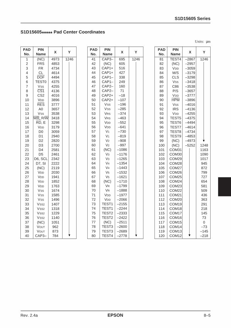
Rev. 2.4a EPSON 8–5
S1D15605***** Pad Center Coordinates
PAD PINX YNo. Name
1 (NC) 4973 12462 FRS 48533 FR 47344 CL 46145 DOF 44946 TEST0 43757 VSS 42558 CS1 41369 CS2 401610 VDD 389611 RES 377712 A0 365713 VSS 353814 WR, R/W 341815 RD, E 329816 VDD 317917 D0 305918 D1 294019 D2 282020 D3 270021 D4 258122 D5 246123 D6, SCL 234224 D7, SI 222225 (NC) 211926 VDD 203027 VDD 194128 VDD 185229 VDD 176330 VSS 167431 VSS 158532 VSS 149633 VSS2 140734 VSS2 131835 VSS2 122936 VSS2 114037 (NC) 105138 VOUT 96239 VOUT 87340 CAP3– 784
PAD PINX YNo. Name
41 CAP3– 695 124642 (NC) 60543 CAP1+ 51644 CAP1+ 42745 CAP1– 33846 CAP1– 24947 CAP2– 16048 CAP2– 7149 CAP2+ –1850 CAP2+ –10751 VSS –19652 VSS –28553 VRS –37454 VRS –46355 VDD –55256 VDD –64157 V1 –73058 V1 –81959 V2 –90860 V2 –99761 (NC) –108662 V3 –117663 V3 –126564 V4 –135465 V4 –144366 V5 –153267 V5 –162168 (NC) –171069 VR –179970 VR –188871 VDD –197772 VDD –206673 TEST1 –215574 TEST1 –224475 TEST2 –233376 TEST2 –242277 (NC) –251178 TEST3 –260079 TEST3 –268980 TEST4 –2778
PAD PINX YNo. Name
81 TEST4 –2867 124682 (NC) –295783 VDD –305984 M/S –317985 CLS –329886 VSS –341887 C86 –353888 P/S –365789 VDD –377790 HPM –389691 VSS –401692 IRS –413693 VDD –425594 TEST5 –437595 TEST6 –449496 TEST7 –461497 TEST8 –473498 TEST9 –485399 (NC) –4973100 (NC) –5252 1248101 COM31 1163102 COM30 1090103 COM29 1017104 COM28 945105 COM27 872106 COM26 799107 COM25 727108 COM24 654109 COM23 581110 COM22 509111 COM21 436112 COM20 363113 COM19 291114 COM18 218115 COM17 145116 COM16 73117 COM15 0118 COM14 –73119 COM13 –145120 COM12 –218
Units: µm

S1D15605 Series
8–6 EPSON Rev. 2.4a
PAD PINX YNo. Name
121 COM11 –5252 –291122 COM10 –363123 COM9 –436124 COM8 –509125 COM7 –581126 COM6 –654127 COM5 –727128 COM4 –800129 COM3 –872130 COM2 –945131 COM1 –1018132 COM0 –1090133 COMS –1163134 (NC) –1248135 (NC) –5009 –1246136 (NC) –4924137 (NC) –4853138 (NC) –4781139 SEG0 –4709140 SEG1 –4637141 SEG2 –4565142 SEG3 –4493143 SEG4 –4421144 SEG5 –4349145 SEG6 –4277146 SEG7 –4206147 SEG8 –4134148 SEG9 –4062149 SEG10 –3990150 SEG11 –3918151 SEG12 –3846152 SEG13 –3774153 SEG14 –3702154 SEG15 –3630155 SEG16 –3559156 SEG17 –3487157 SEG18 –3415158 SEG19 –3343159 SEG20 –3271160 SEG21 –3199
PAD PINX YNo. Name
161 SEG22 –3127 –1246162 SEG23 –3055163 SEG24 –2983164 SEG25 –2912165 SEG26 –2840166 SEG27 –2768167 SEG28 –2696168 SEG29 –2624169 SEG30 –2552170 SEG31 –2480171 SEG32 –2408172 SEG33 –2336173 SEG34 –2265174 SEG35 –2193175 SEG36 –2121176 SEG37 –2049177 SEG38 –1977178 SEG39 –1905179 SEG40 –1833180 SEG41 –1761181 SEG42 –1689182 SEG43 –1618183 SEG44 –1546184 SEG45 –1474185 SEG46 –1402186 SEG47 –1330187 SEG48 –1258188 SEG49 –1186189 SEG50 –1114190 SEG51 –1042191 SEG52 –971192 SEG53 –899193 SEG54 –827194 SEG55 –755195 SEG56 –683196 SEG57 –611197 SEG58 –539198 SEG59 –467199 SEG60 –395200 SEG61 –324
PAD PINX YNo. Name
201 SEG62 –252 –1246202 SEG63 –180203 SEG64 –108204 SEG65 –36205 SEG66 36206 SEG67 108207 SEG68 180208 SEG69 252209 SEG70 324210 SEG71 395211 SEG72 467212 SEG73 539213 SEG74 611214 SEG75 683215 SEG76 755216 SEG77 827217 SEG78 899218 SEG79 971219 SEG80 1042220 SEG81 1114221 SEG82 1186222 SEG83 1258223 SEG84 1330224 SEG85 1402225 SEG86 1474226 SEG87 1546227 SEG88 1618228 SEG89 1689229 SEG90 1761230 SEG91 1833231 SEG92 1905232 SEG93 1977233 SEG94 2049234 SEG95 2121235 SEG96 2193236 SEG97 2265237 SEG98 2336238 SEG99 2408239 SEG100 2480240 SEG101 2552
Units: µm
S1D15605 Series
Rev. 2.4a EPSON 8–7
Units: µm
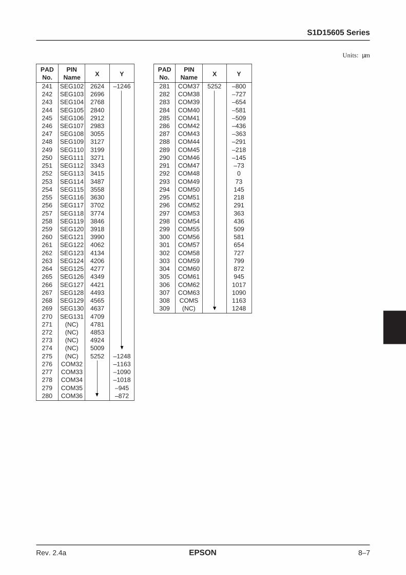
PAD PINX YNo. Name
241 SEG102 2624 –1246242 SEG103 2696243 SEG104 2768244 SEG105 2840245 SEG106 2912246 SEG107 2983247 SEG108 3055248 SEG109 3127249 SEG110 3199250 SEG111 3271251 SEG112 3343252 SEG113 3415253 SEG114 3487254 SEG115 3558255 SEG116 3630256 SEG117 3702257 SEG118 3774258 SEG119 3846259 SEG120 3918260 SEG121 3990261 SEG122 4062262 SEG123 4134263 SEG124 4206264 SEG125 4277265 SEG126 4349266 SEG127 4421267 SEG128 4493268 SEG129 4565269 SEG130 4637270 SEG131 4709271 (NC) 4781272 (NC) 4853273 (NC) 4924274 (NC) 5009275 (NC) 5252 –1248276 COM32 –1163277 COM33 –1090278 COM34 –1018279 COM35 –945280 COM36 –872
PAD PINX YNo. Name
281 COM37 5252 –800282 COM38 –727283 COM39 –654284 COM40 –581285 COM41 –509286 COM42 –436287 COM43 –363288 COM44 –291289 COM45 –218290 COM46 –145291 COM47 –73292 COM48 0293 COM49 73294 COM50 145295 COM51 218296 COM52 291297 COM53 363298 COM54 436299 COM55 509300 COM56 581301 COM57 654302 COM58 727303 COM59 799304 COM60 872305 COM61 945306 COM62 1017307 COM63 1090308 COMS 1163309 (NC) 1248

S1D15605 Series
8–8 EPSON Rev. 2.4a
S1D15606***** Pad Center Coordinates
PAD PINX YNo. Name
1 (NC) 4973 12462 FRS 48533 FR 47344 CL 46145 DOF 44946 TEST0 43757 VSS 42558 CS1 41369 CS2 401610 VDD 389611 RES 377712 A0 365713 VSS 353814 WR, R/W 341815 RD, E 329816 VDD 317917 D0 305918 D1 294019 D2 282020 D3 270021 D4 258122 D5 246123 D6, SCL 234224 D7, SI 222225 (NC) 211926 VDD 203027 VDD 194128 VDD 185229 VDD 176330 VSS 167431 VSS 158532 VSS 149633 VSS2 140734 VSS2 131835 VSS2 122936 VSS2 114037 (NC) 105138 VOUT 96239 VOUT 87340 CAP3– 784
PAD PINX YNo. Name
41 CAP3– 695 124642 (NC) 60543 CAP1+ 51644 CAP1+ 42745 CAP1– 33846 CAP1– 24947 CAP2– 16048 CAP2– 7149 CAP2+ –1850 CAP2+ –10751 VSS –19652 VSS –28553 VRS –37454 VRS –46355 VDD –55256 VDD –64157 V1 –73058 V1 –81959 V2 –90860 V2 –99761 (NC) –108662 V3 –117663 V3 –126564 V4 –135465 V4 –144366 V5 –153267 V5 –162168 (NC) –171069 VR –179970 VR –188871 VDD –197772 VDD –206673 TEST1 –215574 TEST1 –224475 TEST2 –233376 TEST2 –242277 (NC) –251178 TEST3 –260079 TEST3 –268980 TEST4 –2778
PAD PINX YNo. Name
81 TEST4 –2867 124682 (NC) –295783 VDD –305984 M/S –317985 CLS –329886 VSS –341887 C86 –353888 P/S –365789 VDD –377790 HPM –389691 VSS –401692 IRS –413693 VDD –425594 TEST5 –437595 TEST6 –449496 TEST7 –461497 TEST8 –473498 TEST9 –485399 (NC) –4973100 (NC) –5252 1248101 (NC) 1163102 (NC) 1090103 COM23 1017104 (NC) 945105 COM22 872106 (NC) 799107 COM21 727108 COM20 654109 COM19 581110 COM18 509111 COM17 436112 COM16 363113 COM15 291114 COM14 218115 COM13 145116 COM12 73117 COM11 0118 COM10 –73119 COM9 –145120 COM8 –218
Units: µm

S1D15605 Series
Rev. 2.4a EPSON 8–9
PAD PINX YNo. Name
121 COM7 –5252 –291122 COM6 –363123 COM5 –436124 COM4 –509125 COM3 –581126 COM2 –654127 COM1 –727128 (NC) –800129 COM0 –872130 (NC) –945131 COMS –1018132 (NC) –1090133 (NC) –1163134 (NC) –1248135 (NC) –5009 –1246136 (NC) –4924137 (NC) –4853138 (NC) –4781139 SEG0 –4709140 SEG1 –4637141 SEG2 –4565142 SEG3 –4493143 SEG4 –4421144 SEG5 –4349145 SEG6 –4277146 SEG7 –4206147 SEG8 –4134148 SEG9 –4062149 SEG10 –3990150 SEG11 –3918151 SEG12 –3846152 SEG13 –3774153 SEG14 –3702154 SEG15 –3630155 SEG16 –3559156 SEG17 –3487157 SEG18 –3415158 SEG19 –3343159 SEG20 –3271160 SEG21 –3199
PAD PINX YNo. Name
161 SEG22 –3127 –1246162 SEG23 –3055163 SEG24 –2983164 SEG25 –2912165 SEG26 –2840166 SEG27 –2768167 SEG28 –2696168 SEG29 –2624169 SEG30 –2552170 SEG31 –2480171 SEG32 –2408172 SEG33 –2336173 SEG34 –2265174 SEG35 –2193175 SEG36 –2121176 SEG37 –2049177 SEG38 –1977178 SEG39 –1905179 SEG40 –1833180 SEG41 –1761181 SEG42 –1689182 SEG43 –1618183 SEG44 –1546184 SEG45 –1474185 SEG46 –1402186 SEG47 –1330187 SEG48 –1258188 SEG49 –1186189 SEG50 –1114190 SEG51 –1042191 SEG52 –971192 SEG53 –899193 SEG54 –827194 SEG55 –755195 SEG56 –683196 SEG57 –611197 SEG58 –539198 SEG59 –467199 SEG60 –395200 SEG61 –324
PAD PINX YNo. Name
201 SEG62 –252 –1246202 SEG63 –180203 SEG64 –108204 SEG65 –36205 SEG66 36206 SEG67 108207 SEG68 180208 SEG69 252209 SEG70 324210 SEG71 395211 SEG72 467212 SEG73 539213 SEG74 611214 SEG75 683215 SEG76 755216 SEG77 827217 SEG78 899218 SEG79 971219 SEG80 1042220 SEG81 1114221 SEG82 1186222 SEG83 1258223 SEG84 1330224 SEG85 1402225 SEG86 1474226 SEG87 1546227 SEG88 1618228 SEG89 1689229 SEG90 1761230 SEG91 1833231 SEG92 1905232 SEG93 1977233 SEG94 2049234 SEG95 2121235 SEG96 2193236 SEG97 2265237 SEG98 2336238 SEG99 2408239 SEG100 2480240 SEG101 2552
Units: µm

S1D15605 Series
8–10 EPSON Rev. 2.4a
Units: µm
PAD PINX YNo. Name
241 SEG102 2624 –1246242 SEG103 2696243 SEG104 2768244 SEG105 2840245 SEG106 2912246 SEG107 2983247 SEG108 3055248 SEG109 3127249 SEG110 3199250 SEG111 3271251 SEG112 3343252 SEG113 3415253 SEG114 3487254 SEG115 3558255 SEG116 3630256 SEG117 3702257 SEG118 3774258 SEG119 3846259 SEG120 3918260 SEG121 3990261 SEG122 4062262 SEG123 4134263 SEG124 4206264 SEG125 4277265 SEG126 4349266 SEG127 4421267 SEG128 4493268 SEG129 4565269 SEG130 4637270 SEG131 4709271 (NC) 4781272 (NC) 4853273 (NC) 4924274 (NC) 5009275 (NC) 5252 –1248276 (NC) –1163277 (NC) –1090278 COM24 –1018279 (NC) –945280 COM25 –872
PAD PINX YNo. Name
281 (NC) 5252 –800282 COM26 –727283 COM27 –654284 COM28 –581285 COM29 –509286 COM30 –436287 COM31 –363288 COM32 –291289 COM33 –218290 COM34 –145291 COM35 –73292 COM36 0293 COM37 73294 COM38 145295 COM39 218296 COM40 291297 COM41 363298 COM42 436299 COM43 509300 COM44 581301 COM45 654302 COM46 727303 (NC) 799304 COM47 872305 (NC) 945306 COMS 1017307 (NC) 1090308 (NC) 1163309 (NC) 1248

S1D15605 Series
Rev. 2.4a EPSON 8–11
PAD PINX YNo. Name
1 (NC) 4973 12462 FRS 48533 FR 47344 CL 46145 DOF 44946 TEST0 43757 VSS 42558 CS1 41369 CS2 401610 VDD 389611 RES 377712 A0 365713 VSS 353814 WR, R/W 341815 RD, E 329816 VDD 317917 D0 305918 D1 294019 D2 282020 D3 270021 D4 258122 D5 246123 D6, SCL 234224 D7, SI 222225 (NC) 211926 VDD 203027 VDD 194128 VDD 185229 VDD 176330 VSS 167431 VSS 158532 VSS 149633 VSS2 140734 VSS2 131835 VSS2 122936 VSS2 114037 (NC) 105138 VOUT 96239 VOUT 87340 CAP3– 784
PAD PINX YNo. Name
41 CAP3– 695 124642 (NC) 60543 CAP1+ 51644 CAP1+ 42745 CAP1– 33846 CAP1– 24947 CAP2– 16048 CAP2– 7149 CAP2+ –1850 CAP2+ –10751 VSS –19652 VSS –28553 VRS –37454 VRS –46355 VDD –55256 VDD –64157 V1 –73058 V1 –81959 V2 –90860 V2 –99761 (NC) –108662 V3 –117663 V3 –126564 V4 –135465 V4 –144366 V5 –153267 V5 –162168 (NC) –171069 VR –179970 VR –188871 VDD –197772 VDD –206673 TEST1 –215574 TEST1 –224475 TEST2 –233376 TEST2 –242277 (NC) –251178 TEST3 –260079 TEST3 –268980 TEST4 –2778
PAD PINX YNo. Name
81 TEST4 –2867 124682 (NC) –295783 VDD –305984 M/S –317985 CLS –329886 VSS –341887 C86 –353888 P/S –365789 VDD –377790 HPM –389691 VSS –401692 IRS –413693 VDD –425594 TEST5 –437595 TEST6 –449496 TEST7 –461497 TEST8 –473498 TEST9 –485399 (NC) –4973100 (NC) –5252 1248101 COM15 1163102 COM15 1090103 COM14 1017104 COM14 945105 COM13 872106 COM13 799107 COM12 727108 COM12 654109 COM11 581110 COM11 509111 COM10 436112 COM10 363113 COM9 291114 COM9 218115 COM8 145116 COM8 73117 COM7 0118 COM7 –73119 COM6 –145120 COM6 –218
S1D15607***** Pad Center Coordinates
Units: µm

S1D15605 Series
8–12 EPSON Rev. 2.4a
PAD PINX YNo. Name
121 COM5 –5252 –291122 COM5 –363123 COM4 –436124 COM4 –509125 COM3 –581126 COM3 –654127 COM2 –727128 COM2 –800129 COM1 –872130 COM1 –945131 COM0 –1018132 COM0 –1090133 COMS –1163134 (NC) –1248135 (NC) –5009 –1246136 (NC) –4924137 (NC) –4853138 (NC) –4781139 SEG0 –4709140 SEG1 –4637141 SEG2 –4565142 SEG3 –4493143 SEG4 –4421144 SEG5 –4349145 SEG6 –4277146 SEG7 –4206147 SEG8 –4134148 SEG9 –4062149 SEG10 –3990150 SEG11 –3918151 SEG12 –3846152 SEG13 –3774153 SEG14 –3702154 SEG15 –3630155 SEG16 –3559156 SEG17 –3487157 SEG18 –3415158 SEG19 –3343159 SEG20 –3271160 SEG21 –3199
PAD PINX YNo. Name
161 SEG22 –3127 –1246162 SEG23 –3055163 SEG24 –2983164 SEG25 –2912165 SEG26 –2840166 SEG27 –2768167 SEG28 –2696168 SEG29 –2624169 SEG30 –2552170 SEG31 –2480171 SEG32 –2408172 SEG33 –2336173 SEG34 –2265174 SEG35 –2193175 SEG36 –2121176 SEG37 –2049177 SEG38 –1977178 SEG39 –1905179 SEG40 –1833180 SEG41 –1761181 SEG42 –1689182 SEG43 –1618183 SEG44 –1546184 SEG45 –1474185 SEG46 –1402186 SEG47 –1330187 SEG48 –1258188 SEG49 –1186189 SEG50 –1114190 SEG51 –1042191 SEG52 –971192 SEG53 –899193 SEG54 –827194 SEG55 –755195 SEG56 –683196 SEG57 –611197 SEG58 –539198 SEG59 –467199 SEG60 –395200 SEG61 –324
PAD PINX YNo. Name
201 SEG62 –252 –1246202 SEG63 –180203 SEG64 –108204 SEG65 –36205 SEG66 36206 SEG67 108207 SEG68 180208 SEG69 252209 SEG70 324210 SEG71 395211 SEG72 467212 SEG73 539213 SEG74 611214 SEG75 683215 SEG76 755216 SEG77 827217 SEG78 899218 SEG79 971219 SEG80 1042220 SEG81 1114221 SEG82 1186222 SEG83 1258223 SEG84 1330224 SEG85 1402225 SEG86 1474226 SEG87 1546227 SEG88 1618228 SEG89 1689229 SEG90 1761230 SEG91 1833231 SEG92 1905232 SEG93 1977233 SEG94 2049234 SEG95 2121235 SEG96 2193236 SEG97 2265237 SEG98 2336238 SEG99 2408239 SEG100 2480240 SEG101 2552
Units: µm

S1D15605 Series
Rev. 2.4a EPSON 8–13
PAD PINX YNo. Name
241 SEG102 2624 –1246242 SEG103 2696243 SEG104 2768244 SEG105 2840245 SEG106 2912246 SEG107 2983247 SEG108 3055248 SEG109 3127249 SEG110 3199250 SEG111 3271251 SEG112 3343252 SEG113 3415253 SEG114 3487254 SEG115 3558255 SEG116 3630256 SEG117 3702257 SEG118 3774258 SEG119 3846259 SEG120 3918260 SEG121 3990261 SEG122 4062262 SEG123 4134263 SEG124 4206264 SEG125 4277265 SEG126 4349266 SEG127 4421267 SEG128 4493268 SEG129 4565269 SEG130 4637270 SEG131 4709271 (NC) 4781272 (NC) 4853273 (NC) 4924274 (NC) 5009275 (NC) 5252 –1248276 COM16 –1163277 COM16 –1090278 COM17 –1018279 COM17 –945280 COM18 –872
PAD PINX YNo. Name
281 COM18 5252 –800282 COM19 –727283 COM19 –654284 COM20 –581285 COM20 –509286 COM21 –436287 COM21 –363288 COM22 –291289 COM22 –218290 COM23 –145291 COM23 –73292 COM24 0293 COM24 73294 COM25 145295 COM25 218296 COM26 291297 COM26 363298 COM27 436299 COM27 509300 COM28 581301 COM28 654302 COM29 727303 COM29 799304 COM30 872305 COM30 945306 COM31 1017307 COM31 1090308 COMS 1163309 (NC) 1248
Units: µm

S1D15605 Series
8–14 EPSON Rev. 2.4a
S1D15608***** Pad Center Coordinates
Units: µm
PAD PINX YNo. Name
1 (NC) 4973 12462 FRS 48533 FR 47344 CL 46145 DOF 44946 TEST0 43757 VSS 42558 CS1 41369 CS2 401610 VDD 389611 RES 377712 A0 365713 VSS 353814 WR, R/W 341815 RD, E 329816 VDD 317917 D0 305918 D1 294019 D2 282020 D3 270021 D4 258122 D5 246123 D6, SCL 234224 D7, SI 222225 (NC) 211926 VDD 203027 VDD 194128 VDD 185229 VDD 176330 VSS 167431 VSS 158532 VSS 149633 VSS2 140734 VSS2 131835 VSS2 122936 VSS2 114037 (NC) 105138 VOUT 96239 VOUT 87340 CAP3– 784
PAD PINX YNo. Name
41 CAP3– 695 124642 (NC) 60543 CAP1+ 51644 CAP1+ 42745 CAP1– 33846 CAP1– 24947 CAP2– 16048 CAP2– 7149 CAP2+ –1850 CAP2+ –10751 VSS –19652 VSS –28553 VRS –37454 VRS –46355 VDD –55256 VDD –64157 V1 –73058 V1 –81959 V2 –90860 V2 –99761 (NC) –108662 V3 –117663 V3 –126564 V4 –135465 V4 –144366 V5 –153267 V5 –162168 (NC) –171069 VR –179970 VR –188871 VDD –197772 VDD –206673 TEST1 –215574 TEST1 –224475 TEST2 –233376 TEST2 –242277 (NC) –251178 TEST3 –260079 TEST3 –268980 TEST4 –2778
PAD PINX YNo. Name
81 TEST4 –2867 124682 (NC) –295783 VDD –305984 M/S –317985 CLS –329886 VSS –341887 C86 –353888 P/S –365789 VDD –377790 HPM –389691 VSS –401692 IRS –413693 VDD –425594 TEST5 –437595 TEST6 –449496 TEST7 –461497 TEST8 –473498 TEST9 –485399 (NC) –4973100 (NC) –5252 1248101 (NC) 1163102 COM26 1090103 (NC) 1017104 COM25 945105 COM25 872106 COM23 799107 COM22 727108 COM21 654109 COM20 581110 COM19 509111 COM18 436112 COM17 363113 COM16 291114 COM15 218115 COM14 145116 COM13 73117 COM12 0118 COM11 –73119 COM10 –145120 COM9 –218

S1D15605 Series
Rev. 2.4a EPSON 8–15
PAD PINX YNo. Name
121 COM8 –5252 –291122 COM7 –363123 COM6 –436124 COM5 –509125 COM4 –581126 COM3 –654127 COM2 –727128 COM1 –800129 (NC) –872130 COM0 –945131 (NC) –1018132 COMS –1090133 (NC) –1163134 (NC) –1248135 (NC) –5009 –1246136 (NC) –4924137 (NC) –4853138 (NC) –4781139 SEG0 –4709140 SEG1 –4637141 SEG2 –4565142 SEG3 –4493143 SEG4 –4421144 SEG5 –4349145 SEG6 –4277146 SEG7 –4206147 SEG8 –4134148 SEG9 –4062149 SEG10 –3990150 SEG11 –3918151 SEG12 –3846152 SEG13 –3774153 SEG14 –3702154 SEG15 –3630155 SEG16 –3559156 SEG17 –3487157 SEG18 –3415158 SEG19 –3343159 SEG20 –3271160 SEG21 –3199
PAD PINX YNo. Name
161 SEG22 –3127 –1246162 SEG23 –3055163 SEG24 –2983164 SEG25 –2912165 SEG26 –2840166 SEG27 –2768167 SEG28 –2696168 SEG29 –2624169 SEG30 –2552170 SEG31 –2480171 SEG32 –2408172 SEG33 –2336173 SEG34 –2265174 SEG35 –2193175 SEG36 –2121176 SEG37 –2049177 SEG38 –1977178 SEG39 –1905179 SEG40 –1833180 SEG41 –1761181 SEG42 –1689182 SEG43 –1618183 SEG44 –1546184 SEG45 –1474185 SEG46 –1402186 SEG47 –1330187 SEG48 –1258188 SEG49 –1186189 SEG50 –1114190 SEG51 –1042191 SEG52 –971192 SEG53 –899193 SEG54 –827194 SEG55 –755195 SEG56 –683196 SEG57 –611197 SEG58 –539198 SEG59 –467199 SEG60 –395200 SEG61 –324
PAD PINX YNo. Name
201 SEG62 –252 –1246202 SEG63 –180203 SEG64 –108204 SEG65 –36205 SEG66 36206 SEG67 108207 SEG68 180208 SEG69 252209 SEG70 324210 SEG71 395211 SEG72 467212 SEG73 539213 SEG74 611214 SEG75 683215 SEG76 755216 SEG77 827217 SEG78 899218 SEG79 971219 SEG80 1042220 SEG81 1114221 SEG82 1186222 SEG83 1258223 SEG84 1330224 SEG85 1402225 SEG86 1474226 SEG87 1546227 SEG88 1618228 SEG89 1689229 SEG90 1761230 SEG91 1833231 SEG92 1905232 SEG93 1977233 SEG94 2049234 SEG95 2121235 SEG96 2193236 SEG97 2265237 SEG98 2336238 SEG99 2408239 SEG100 2480240 SEG101 2552
Units: µm

S1D15605 Series
8–16 EPSON Rev. 2.4a
PAD PINX YNo. Name
241 SEG102 2624 –1246242 SEG103 2696243 SEG104 2768244 SEG105 2840245 SEG106 2912246 SEG107 2983247 SEG108 3055248 SEG109 3127249 SEG110 3199250 SEG111 3271251 SEG112 3343252 SEG113 3415253 SEG114 3487254 SEG115 3558255 SEG116 3630256 SEG117 3702257 SEG118 3774258 SEG119 3846259 SEG120 3918260 SEG121 3990261 SEG122 4062262 SEG123 4134263 SEG124 4206264 SEG125 4277265 SEG126 4349266 SEG127 4421267 SEG128 4493268 SEG129 4565269 SEG130 4637270 SEG131 4709271 (NC) 4781272 (NC) 4853273 (NC) 4924274 (NC) 5009275 (NC) 5252 –1248276 (NC) –1163277 COM27 –1090278 (NC) –1018279 COM28 –945280 (NC) –872
PAD PINX YNo. Name
281 COM29 5252 –800282 COM30 –727283 COM31 –654284 COM32 –581285 COM33 –509286 COM34 –436287 COM35 –363288 COM36 –291289 COM37 –218290 COM38 –145291 COM39 –73292 COM40 0293 COM41 73294 COM42 145295 COM43 218296 COM44 291297 COM45 363298 COM46 436299 COM47 509300 COM48 581301 COM48 654302 COM50 727303 COM51 799304 COM52 872305 COM53 945306 (NC) 1017307 COMS 1090308 (NC) 1163309 (NC) 1248
Units: µm

S1D15605 Series
Rev. 2.4a EPSON 8–17
PAD PINX YNo. Name
1 (NC) 4973 12462 FRS 48533 FR 47344 CL 46145 DOF 44946 TEST0 43757 VSS 42558 CS1 41369 CS2 401610 VDD 389611 RES 377712 A0 365713 VSS 353814 WR, R/W 341815 RD, E 329816 VDD 317917 D0 305918 D1 294019 D2 282020 D3 270021 D4 258122 D5 246123 D6, SCL 234224 D7, SI 222225 (NC) 211926 VDD 203027 VDD 194128 VDD 185229 VDD 176330 VSS 167431 VSS 158532 VSS 149633 VSS2 140734 VSS2 131835 VSS2 122936 VSS2 114037 (NC) 105138 VOUT 96239 VOUT 87340 CAP3– 784
PAD PINX YNo. Name
41 CAP3– 695 124642 (NC) 60543 CAP1+ 51644 CAP1+ 42745 CAP1– 33846 CAP1– 24947 CAP2– 16048 CAP2– 7149 CAP2+ –1850 CAP2+ –10751 VSS –19652 VSS –28553 VRS –37454 VRS –46355 VDD –55256 VDD –64157 V1 –73058 V1 –81959 V2 –90860 V2 –99761 (NC) –108662 V3 –117663 V3 –126564 V4 –135465 V4 –144366 V5 –153267 V5 –162168 (NC) –171069 VR –179970 VR –188871 VDD –197772 VDD –206673 TEST1 –215574 TEST1 –224475 TEST2 –233376 TEST2 –242277 (NC) –251178 TEST3 –260079 TEST3 –268980 TEST4 –2778
PAD PINX YNo. Name
81 TEST4 –2867 124682 (NC) –295783 VDD –305984 M/S –317985 CLS –329886 VSS –341887 C86 –353888 P/S –365789 VDD –377790 HPM –389691 VSS –401692 IRS –413693 VDD –425594 TEST5 –437595 TEST6 –449496 TEST7 –461497 TEST8 –473498 TEST9 –485399 (NC) –4973100 (NC) –5252 1248101 (NC) 1163102 COM25 1090103 (NC) 1017104 COM24 945105 (NC) 872106 COM23 799107 COM22 727108 COM21 654109 COM20 581110 COM19 509111 COM18 436112 COM17 363113 COM16 291114 COM15 218115 COM14 145116 COM13 73117 COM12 0118 COM11 –73119 COM10 –145120 COM9 –218
S1D15609***** Pad Center Coordinates
Units: µm

S1D15605 Series
8–18 EPSON Rev. 2.4a
PAD PINX YNo. Name
121 COM8 –5252 –291122 COM7 –363123 COM6 –436124 COM5 –509125 COM4 –581126 COM3 –654127 COM2 –727128 COM1 –800129 (NC) –872130 COM0 –945131 (NC) –1018132 COMS –1090133 (NC) –1163134 (NC) –1248135 (NC) –5009 –1246136 (NC) –4924137 (NC) –4853138 (NC) –4781139 SEG0 –4709140 SEG1 –4637141 SEG2 –4565142 SEG3 –4493143 SEG4 –4421144 SEG5 –4349145 SEG6 –4277146 SEG7 –4206147 SEG8 –4134148 SEG9 –4062149 SEG10 –3990150 SEG11 –3918151 SEG12 –3846152 SEG13 –3774153 SEG14 –3702154 SEG15 –3630155 SEG16 –3559156 SEG17 –3487157 SEG18 –3415158 SEG19 –3343159 SEG20 –3271160 SEG21 –3199
PAD PINX YNo. Name
161 SEG22 –3127 –1246162 SEG23 –3055163 SEG24 –2983164 SEG25 –2912165 SEG26 –2840166 SEG27 –2768167 SEG28 –2696168 SEG29 –2624169 SEG30 –2552170 SEG31 –2480171 SEG32 –2408172 SEG33 –2336173 SEG34 –2265174 SEG35 –2193175 SEG36 –2121176 SEG37 –2049177 SEG38 –1977178 SEG39 –1905179 SEG40 –1833180 SEG41 –1761181 SEG42 –1689182 SEG43 –1618183 SEG44 –1546184 SEG45 –1474185 SEG46 –1402186 SEG47 –1330187 SEG48 –1258188 SEG49 –1186189 SEG50 –1114190 SEG51 –1042191 SEG52 –971192 SEG53 –899193 SEG54 –827194 SEG55 –755195 SEG56 –683196 SEG57 –611197 SEG58 –539198 SEG59 –467199 SEG60 –395200 SEG61 –324
PAD PINX YNo. Name
201 SEG62 –252 –1246202 SEG63 –180203 SEG64 –108204 SEG65 –36205 SEG66 36206 SEG67 108207 SEG68 180208 SEG69 252209 SEG70 324210 SEG71 395211 SEG72 467212 SEG73 539213 SEG74 611214 SEG75 683215 SEG76 755216 SEG77 827217 SEG78 899218 SEG79 971219 SEG80 1042220 SEG81 1114221 SEG82 1186222 SEG83 1258223 SEG84 1330224 SEG85 1402225 SEG86 1474226 SEG87 1546227 SEG88 1618228 SEG89 1689229 SEG90 1761230 SEG91 1833231 SEG92 1905232 SEG93 1977233 SEG94 2049234 SEG95 2121235 SEG96 2193236 SEG97 2265237 SEG98 2336238 SEG99 2408239 SEG100 2480240 SEG101 2552
Units: µm

S1D15605 Series
Rev. 2.4a EPSON 8–19
PAD PINX YNo. Name
241 SEG102 2624 –1246242 SEG103 2696243 SEG104 2768244 SEG105 2840245 SEG106 2912246 SEG107 2983247 SEG108 3055248 SEG109 3127249 SEG110 3199250 SEG111 3271251 SEG112 3343252 SEG113 3415253 SEG114 3487254 SEG115 3558255 SEG116 3630256 SEG117 3702257 SEG118 3774258 SEG119 3846259 SEG120 3918260 SEG121 3990261 SEG122 4062262 SEG123 4134263 SEG124 4206264 SEG125 4277265 SEG126 4349266 SEG127 4421267 SEG128 4493268 SEG129 4565269 SEG130 4637270 SEG131 4709271 (NC) 4781272 (NC) 4853273 (NC) 4924274 (NC) 5009275 (NC) 5252 –1248276 (NC) –1163277 COM26 –1090278 (NC) –1018279 COM27 –945280 (NC) –872
PAD PINX YNo. Name
281 COM28 5252 –800282 COM29 –727283 COM30 –654284 COM31 –581285 COM32 –509286 COM33 –436287 COM34 –363288 COM35 –291289 COM36 –218290 COM37 –145291 COM38 –73292 COM39 0293 COM40 73294 COM41 145295 COM42 218296 COM43 291297 COM44 363298 COM45 436299 COM46 509300 COM47 581301 COM48 654302 COM49 727303 COM50 799304 (NC) 872305 COM51 945306 (NC) 1017307 COMS 1090308 (NC) 1163309 (NC) 1248
Units: µm

S1D15605 Series
8–20 EPSON Rev. 2.4a
5. PIN DESCRIPTIONSPower Supply Pins
Pin Name I/O Function No. ofPins
VDD Power Shared with the MPU power supply terminal VCC. 13Supply
VSS Power This is a 0V terminal connected to the system GND. 9Supply
VSS2 Power This is the reference power supply for the step-up voltage circuit for the 4Supply liquid crystal drive.
VRS Power This is the externally-input VREG power supply for the LCD power supply 2Supply voltage regulator.
These are only enabled for the models with the VREG external input option.
V1, V2, Power This is a multi-level power supply for the liquid crystal drive. The voltage 10V3, V4, Supply applied is determined by the liquid crystal cell, and is changed through theV5 use of a resistive voltage divided or through changing the impedance using
an op. amp. Voltage levels are determined based on VDD, and mustmaintain the relative magnitudes shown below.
VDD (= V0) ≥ V1 ≥ V2 ≥ V3 ≥ V4 ≥ V5
Master operation: When the power supply turns ON, the internal powersupply circuits produce the V1 to V4 voltages shown below. The voltagesettings are selected using the LCD bias set command.
LCD Power Supply Circuit Terminals
Pin Name I/O Function No. ofPins
CAP1+ O DC/DC voltage converter. Connect a capacitor between this terminal and 2the CAP1- terminal.
CAP1– O DC/DC voltage converter. Connect a capacitor between this terminal and 2the CAP1+ terminal.
CAP2+ O DC/DC voltage converter. Connect a capacitor between this terminal and 2the CAP2- terminal.
CAP2– O DC/DC voltage converter. Connect a capacitor between this terminal and 2the CAP2+ terminal.
CAP3– O DC/DC voltage converter. Connect a capacitor between this terminal and 2the CAP1+ terminal.
VOUT I/O DC/DC voltage converter. Connect a capacitor between this terminal and 2VSS2.
VR I Output voltage regulator terminal. Provides the voltage between VDD and 2V5 through a resistive voltage divider.These are only enabled when the V5 voltage regulator internal resistors arenot used (IRS = LOW).These cannot be used when the V5 voltage regulator internal resistors areused (IRS = HIGH).
S1D15605***** S1D15606***** S1D15607***** S1D15608***** S1D15609*****V1 1/9•V5 1/7•V5 1/8•V5 1/6•V5 1/6•V5 1/5•V5 1/8•V5 1/6•V5 1/8•V5 1/6•V5V2 2/9•V5 2/7•V5 2/8•V5 2/6•V5 2/6•V5 2/5•V5 2/8•V5 2/6•V5 2/8•V5 2/6•V5V3 7/9•V5 5/7•V5 6/8•V5 4/6•V5 4/6•V5 3/5•V5 6/8•V5 4/6•V5 6/8•V5 4/6•V5V4 8/9•V5 6/7•V5 7/8•V5 5/6•V5 5/6•V5 4/5•V5 7/8•V5 5/6•V5 7/6•V5 5/6•V5

S1D15605 Series
Rev. 2.4a EPSON 8–21
Pin Name I/O Function No. ofPins
D7 to D0 I/O This is an 8-bit bi-directional data bus that connects to an 8-bit or 16-bit 8standard MPU data bus.
(SI) When the serial interface is selected (P/S = LOW), then D7 serves as the(SCL) serial data input terminal (SI) and D6 serves as the serial clock input
terminal (SCL). At this time, D0 to D5 are set to high impedance.When the chip select is inactive, D0 to D7 are set to high impedance.
A0 I This is connect to the least significant bit of the normal MPU address bus, 1and it determines whether the data bits are data or a command.A0 = HIGH: Indicates that D0 to D7 are display data.A0 = LOW: Indicates that D0 to D7 are display control data.
RES I When RES is set to LOW, the settings are initialized. 1The reset operation is performed by the RES signal level.
CS1 I This is the chip select signal. When CS1 = LOW and CS2 = HIGH, then the 2CS2 chip select becomes active, and data/command I/O is enabled.
RD I • When connected to an 8080 MPU, this is active LOW. 1(E) This pin is connected to the RD signal of the 8080 MPU, and the
S1D15605 series data bus is in an output status when this signal is LOW.• When connected to a 6800 Series MPU, this is active HIGH.
This is the 6800 Series MPU enable clock input terminal.
WR I • When connected to an 8080 MPU, this is active LOW. 1(R/W) This terminal connects to the 8080 MPU WR signal. The signals on
the data bus are latched at the rising edge of the WR signal.• When connected to a 6800 Series MPU:
This is the read/write control signal input terminal.When R/W = HIGH: Read.When R/W = LOW: Write.
C86 I This is the MPU interface switch terminal. 1C86 = HIGH: 6800 Series MPU interface.C86 = LOW: 8080 MPU interface.
P/S I This is the parallel data input/serial data input switch terminal. 1P/S = HIGH: Parallel data input.P/S = LOW: Serial data input.The following applies depending on the P/S status:
When P/S = LOW, D0 to D5 are HZ. D0 to D5 may be HIGH, LOW or Open.RD (E) and WR (P/W) are fixed to either HGIH or LOW.With serial data input, RAM display data reading is not supported.
CLS I Terminal to select whether or enable or disable the display clock internal 1oscillator circuit.
CLS = HIGH: Internal oscillator circuit is enabledCLS = LOW: Internal oscillator circuit is disabled (requires external input)
When CLS = LOW, input the display clock through the CL terminal.
When using the S1D15605 Series as a master or slave, set respectiveCLS pins at the same level.
System Bus Connection Terminals
P/S Data/Command Data Read/Write Serial ClockHIGH A0 D0 to D7 RD, WRLOW A0 SI (D7) Write only SCL (D6)
Display clock Master SlaveBuilt-in oscillator circuit used HIGH HIGHExternal input LOW LOW

S1D15605 Series
8–22 EPSON Rev. 2.4a
Pin Name I/O Function No. ofPins
M/S I This terminal selects the master/slave operation for the S1D15605 Series 1chips. Master operation outputs the timing signals that are required for theLCD display, while slave operation inputs the timing signals required for theliquid crystal display, synchronizing the liquid crystal display system.
M/S = HIGH: Master operationM/S = LOW: Slave operation
The following is true depending on the M/S and CLS status:
CL I/O This is the display clock input terminal 1The following is true depending on the M/S and CLS status.
When the S1D15605 Series chips are used in master/slave mode, thevarious CL terminals must be connected.
FR I/O This is the liquid crystal alternating current signal I/O terminal. 1M/S = HIGH: OutputM/S = LOW: Input
When the S1D15605 Series chip is used in master/slave mode, the variousFR terminals must be connected.
DOF I/O This is the liquid crystal display blanking control terminal. 1M/S = HIGH: OutputM/S = LOW: Input
When the S1D15605 Series chip is used in master/slave mode, the variousDOF terminals must be connected.
FRS O This is the output terminal for the static drive. 1This terminal is only enabled when the static indicator display is ON whenin master operation mode, and is used in conjunction with the FR terminal.
IRS I This terminal selects the resistors for the V5 voltage level adjustment. 1IRS = HIGH: Use the internal resistorsIRS = LOW: Do not use the internal resistors. The V5 voltage level is
regulated by an external resistive voltage divider attached to the VRterminal.This pin is enabled only when the master operation mode is selected.It is fixed to either HIGH or LOW when the slave operation mode is selected.
HPM I This is the power control terminal for the power supply circuit for liquid 1crystal drive.
HPM = HIGH: Normal modeHPM = LOW: High power mode
This pin is enabled only when the master operation mode is selected.It is fixed to either HIGH or LOW when the slave operation mode is selected.
OscillatorPower
M/S CLSCircuit
Supply CL FR FRS DOFCircuit
HIGH HIGH Enabled Enabled Output Output Output OutputLOW Disabled Enabled Input Output Output Output
LOW HIGH Disabled Disabled Input Input Output InputLOW Disabled Disabled Input Input Output Input
M/S CLS CLHIGH HIGH Output
LOW Input
LOW HIGH InputLOW Input
S1D15605 Series
Rev. 2.4a EPSON 8–23
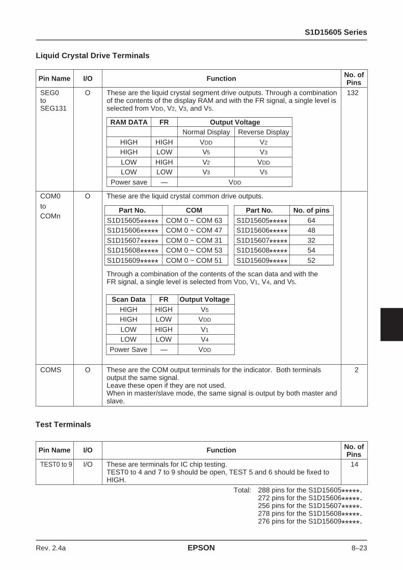
Pin Name I/O Function No. ofPins
SEG0 O These are the liquid crystal segment drive outputs. Through a combination 132to of the contents of the display RAM and with the FR signal, a single level isSEG131 selected from VDD, V2, V3, and V5.
COM0 O These are the liquid crystal common drive outputs.
toCOMn
Through a combination of the contents of the scan data and with theFR signal, a single level is selected from VDD, V1, V4, and V5.
COMS O These are the COM output terminals for the indicator. Both terminals 2output the same signal.Leave these open if they are not used.When in master/slave mode, the same signal is output by both master andslave.
Liquid Crystal Drive Terminals
RAM DATA FR Output VoltageNormal Display Reverse Display
HIGH HIGH VDD V2
HIGH LOW V5 V3
LOW HIGH V2 VDD
LOW LOW V3 V5
Power save — VDD
Scan Data FR Output VoltageHIGH HIGH V5
HIGH LOW VDD
LOW HIGH V1
LOW LOW V4
Power Save — VDD
Test Terminals
Pin Name I/O Function No. ofPins
TEST0 to 9 I/O These are terminals for IC chip testing. 14TEST0 to 4 and 7 to 9 should be open, TEST 5 and 6 should be fixed toHIGH.
Total: 288 pins for the S1D15605*****.272 pins for the S1D15606*****.256 pins for the S1D15607*****.278 pins for the S1D15608*****.276 pins for the S1D15609*****.
Part No. COMS1D15605***** COM 0 ~ COM 63S1D15606***** COM 0 ~ COM 47
S1D15607***** COM 0 ~ COM 31S1D15608***** COM 0 ~ COM 53
S1D15609***** COM 0 ~ COM 51
Part No. No. of pinsS1D15605***** 64S1D15606***** 48
S1D15607***** 32S1D15608***** 54
S1D15609***** 52

S1D15605 Series
8–24 EPSON Rev. 2.4a
6. DESCRIPTION OF FUNCTIONSThe MPU InterfaceSelecting the Interface Type
With the S1D15605 Series chips, data transfers are donethrough an 8-bit bi-directional data bus (D7 to D0) or
through a serial data input (SI). Through selecting the P/S terminal polarity to the HIGH or LOW it is possible toselect either parallel data input or serial data input asshown in Table 1.
The Parallel Interface
When the parallel interface has been selected (P/S =HIGH), then it is possible to connect directly to either an
8080-system MPU or a 6800 Series MPU (as shown inTable 2) by selecting the C86 terminal to either HIGHor to LOW.
Moreover, data bus signals are recognized by acombination of A0, RD (E), WR (R/W) signals, asshown in Table 3.
Table 3Shared 6800 Series 8080 Series
FunctionA0 R/W RD WR1 1 0 1 Reads the display data1 0 1 0 Writes the display data
0 1 0 1 Status read0 0 1 0 Write control data (command)
Table 2
P/S CS1 CS2 A0 RD WR D7~D0HIGH: 6800 Series MPU Bus CS1 CS2 A0 E R/W D7~D0LOW: 8080 MPU Bus CS1 CS2 A0 RD WR D7~D0
Table 1P/S CS1 CS2 A0 RD WR C86 D7 D6 D5~D0
HIGH: Parallel Input CS1 CS2 A0 RD WR C86 D7 D6 D5~D0LOW: Serial Input CS1 CS2 A0 — — — SI SCL (HZ)
“—” indicates fixed to either HIGH or to LOW. HZ is in the state of High Impedance.

S1D15605 Series
Rev. 2.4a EPSON 8–25
The Serial Interface
When the serial interface has been selected (P/S =LOW) then when the chip is in active state (CS1 = LOWand CS2 = HIGH) the serial data input (SI) and the serialclock input (SCL) can be received. The serial data isread from the serial data input pin in the rising edge ofthe serial clocks D7, D6 through D0, in this order. Thisdata is converted to 8 bits parallel data in the rising edge
of the eighth serial clock for the processing.The A0 input is used to determine whether or the serialdata input is display data or command data; when A0 =HIGH, the data is display data, and when A0 = LOWthen the data is command data. The A0 input is read andused for detection every 8th rising edge of the serialclock after the chip becomes active.Figure 1 is a serial interface signal chart.
Figure 1
* When the chip is not active, the shift registers and the counter are reset to their initial states.* Reading is not possible while in serial interface mode.* Caution is required on the SCL signal when it comes to line-end reflections and external noise. We recommend that
operation be rechecked on the actual equipment.
The Chip Select
The S1D15605 Series chips have two chip selectterminals: CS1 and CS2. The MPU interface or theserial interface is enabled only when CS1 = LOW andCS2 = HIGH.When the chip select is inactive, D0 to D7 enter a highimpedance state, and the A0, RD, and WR inputs areinactive. When the serial interface is selected, the shiftregister and the counter are reset.
Accessing the Display Data RAM and theInternal Registers
Data transfer at a higher speed is ensured since the MPUis required to satisfy the cycle time (tCYC) requirementalone in accessing the S1D15605 Series. Wait time maynot be considered.And, in the S1D15605 Series chips, each time data issent from the MPU, a type of pipeline process between
LSIs is performed through the bus holder attached to theinternal data bus.For example, when the MPU writes data to the displaydata RAM, once the data is stored in the bus holder, thenit is written to the display data RAM before the next datawrite cycle. Moreover, when the MPU reads the displaydata RAM, the first data read cycle (dummy) stores theread data in the bus holder, and then the data is read fromthe bus holder to the system bus at the next data readcycle.There is a certain restriction in the read sequence of thedisplay data RAM. Please be advised that data of thespecified address is not generated by the read instructionissued immediately after the address setup. This data isgenerated in data read of the second time. Thus, adummy read is required whenever the address setup orwrite cycle operation is conducted.This relationship is shown in Figure 2.
CS1
CS2SI
SCL
A0
D7
1 2 3 4 5 6 7 8 9 10 11 12 13 14
D6 D5 D4 D3 D2 D7 D6 D5 D4 D3 D2D1 D0

S1D15605 Series
8–26 EPSON Rev. 2.4a
The Busy Flag
When the busy flag is “1” it indicates that the S1D15605Series chip is running internal processes, and at thistime no command aside from a status read will bereceived. The busy flag is outputted to D7 pin with the
N
N
N+1 N+2 N+3
N+1 N+2 N+3
WR
MP
UIn
tern
al T
imin
g
DATA
Latch
BUS Holder
Write Signal
N N n n+1
N+2Increment N+1Preset N
N n n+1 n+2
Data Read#n+1
Data Read#n
DummyRead
Address Set#n
Inte
rnal
Tim
ing
WR
RD
DATA
Address Preset
Read Signal
Column Address
Bus Holder
MP
U
Writing
Reading
read instruction. If the cycle time (tCYC) is maintained,it is not necessary to check for this flag before eachcommand. This makes vast improvements in MPUprocessing capabilities possible.
Figure 2

S1D15605 Series
Rev. 2.4a EPSON 8–27
D0
D1
D2
D3
D4
—
0
1
0
0
1
1
0
0
1
0
1
0
0
1
0
1
0
0
1
0
0
0
0
0
0
Display data RAM
COM0
COM1
COM2
COM3
COM4
—
Liquid crystal display
Display Data RAMDisplay Data RAM
The display data RAM is a RAM that stores the dot datafor the display. It has a 65 (8 page × 8 bit +1) × 132 bitstructure. It is possible to access the desired bit byspecifying the page address and the column address.Because, as is shown in Figure 3, the D7 to D0 displaydata from the MPU corresponds to the liquid crystaldisplay common direction, there are few constraints at
the time of display data transfer when multiple S1D15605series chips are used, thus and display structures can becreated easily and with a high degree of freedom.Moreover, reading from and writing to the displayRAM from the MPU side is performed through the I/Obuffer, which is an independent operation from signalreading for the liquid crystal driver. Consequently, evenif the display data RAM is accessed asynchronouslyduring liquid crystal display, it will not cause adverseeffects on the display (such as flickering).
Table 4
SEGSEG0 SEG 131Output
ADC “0” 0 (H) → Column Address → 83 (H)(D0) “1” 83 (H) ← Column Address ← 0 (H)
Figure 3
The Page Address Circuit
As shown in Figure 6-4, page address of the display dataRAM is specified through the Page Address SetCommand. The page address must be specified againwhen changing pages to perform access.Page address 8 (D3, D2, D1, D0 = 1, 0, 0, 0) is the pagefor the RAM region used only by the indicators, andonly display data D0 is used.
The Column Addresses
As is shown in Figure 4, the display data RAM columnaddress is specified by the Column Address Setcommand. The specified column address is incremented(+1) with each display data read/write command. Thisallows the MPU display data to be accessed continuously.Moreover, the incrementation of column addresses stopswith 83H. Because the column address is independentof the page address, when moving, for example, frompage 0 column 83H to page 1 column 00H, it is necessaryto respecify both the page address and the columnaddress.Furthermore, as is shown in Table 4, the ADC command(segment driver direction select command) can be usedto reverse the relationship between the display dataRAM column address and the segment output. Becauseof this, the constraints on the IC layout when the LCDmodule is assembled can be minimized.
The Line Address Circuit
The line address circuit, as shown in Table 4, specifiesthe line address relating to the COM output when thecontents of the display data RAM are displayed. Usingthe display start line address set command, what isnormally the top line of the display can be specified (thisis the COM0 output when the common output mode isnormal, and the COM63 output for S1D15605 Series,COM47 output for S1D15606 Series, COM31 output forthe S1D15607 Series, COM53 output for S1D15608*****and COM51 output for S1D15609***** ) when the commonoutput mode is reversed. The display area is a 65 line areafor the S1D15605 Series, a 49 line are for the S1D15606,a 33 line area for the S1D15607 Series , 55 line area forthe S1D15608***** and 53 line area for theS1D15609***** from the display start line address.If the line addresses are changed dynamically using thedisplay start line address set command, screen scrolling,page swapping, etc. can be performed.

S1D15605 Series
8–28 EPSON Rev. 2.4a
D0D1D2D3D4D5D6D7D0D1D2D3D4D5D6D7D0D1D2D3D4D5D6D7D0D1D2D3D4D5D6D7D0D1D2D3D4D5D6D7D0D1D2D3D4D5D6D7D0D1D2D3D4D5D6D7D0D1D2D3D4D5D6D7D0
00H01H02H03H04H05H06H07H08H09H0AH0BH0CH0DH0EH0FH11H12H13H14H15H16H17H18H18H19H1AH1BH1CH1DH1EH1FH20H21H22H23H24H25H26H27H28H29H2AH2BH2CH2DH2EH2FH30H31H32H33H34H35H36H37H38H39H3AH3BH3CH3DH3EH3FH
COM0COM1COM2COM3COM4COM5COM6COM7COM8COM9
COM10COM11COM12COM13COM14COM15COM16COM17COM18COM19COM20COM21COM22COM23COM24COM25COM26COM27COM28COM29COM30COM31COM32COM33COM34COM35COM36COM37COM38COM39COM40COM41COM42COM43COM44COM45COM46COM47COM48COM49COM50COM51COM52COM53COM54COM55COM56COM57COM58COM59COM60COM61COM62COM63COMS
0 0 0 0 Page 0
0 0 0 1 Page 1
0 0 1 0 Page 2
0 0 1 1 Page 3
0 1 0 0 Page 4
0 1 0 1 Page 5
0 1 1 0 Page 6
0 1 1 1 Page 7
1 0 0 0 Page 8
SE
G0
SE
G1
SE
G2
SE
G3
SE
G4
SE
G5
SE
G6
SE
G7
83 82 81 80 7F 7E 7D 7C
00 01 02 03 04 05 06 07
SE
G12
7S
EG
125
SE
G12
6S
EG
127
SE
G12
8S
EG
129
SE
G13
0S
EG
131
07 06 05 04 03 02 01 00
7C 7D 7E 7F 80 81 82 83
LCD
Out
AD
C
Col
umn
Add
ress
1 D0
0 D0 Regardless of the display
start line address, the S1D15605 Series accesses 65th line, the S1D15606 Series accesses 49th line and the S1D15607 Series accesses 33th line and the S1D15608 Series accesses 55th line, the S1D15609 Series accesses 53 lines.
Start
63 li
nes
52 li
nes
48 li
nes
Page AddressD3 D2 D1 D0 Data
LineAddress
COMOutput
When the common output mode is normal
32 li
nes
54 li
nes
Figure 4

S1D15605 Series
Rev. 2.4a EPSON 8–29
The Display Data Latch Circuit
The display data latch circuit is a latch that temporarilystores the display data that is output to the liquid crystaldriver circuit from the display data RAM.Because the display normal/reverse status, display ON/OFF status, and display all points ON/OFF commandscontrol only the data within the latch, they do not changethe data within the display data RAM itself.
The Oscillator CircuitThis is a CR-type oscillator that produces the displayclock. The oscillator circuit is only enabled when M/S= HIGH and CLS = HIGH.When CLS = LOW the oscillation stops, and the displayclock is input through the CL terminal.
Display Timing Generator CircuitThe display timing generator circuit generates the timingsignal to the line address circuit and the display datalatch circuit using the display clock. The display data islatched into the display data latch circuit synchronizedwith the display clock, and is output to the data driveroutput terminal. Reading to the display data liquidcrystal driver circuits is completely independent ofaccesses to the display data RAM by the MPU.Consequently, even if the display data RAM is accessedasynchronously during liquid crystal display, there isabsolutely no adverse effect (such as flickering) on thedisplay.Moreover, the display timing generator circuit generatesthe common timing and the liquid crystal alternatingcurrent signal (FR) from the display clock. It generatesa drive wave form using a 2 frame alternating currentdrive method, as is shown in Figure 5, for the liquidcrystal drive circuit.
Figure 5
64CL
FR
COM0
VDD
VDD
VDD
V1
V1
V4
V5
V4
V2
V3
V5
V5
COM1
RAMDATA
SEGn
65 1 2 3 4 5 6 60 61 62 63 64 65 1 2 3 4 5 6
Two-frame alternating current drive wave form (S1D15605 *****)

S1D15605 Series
8–30 EPSON Rev. 2.4a
When multiple S1D15605 Series chips are used, theslave chips must be supplied the display timing signals(FR, CL, DOF) from the master chip[s].Table 5 shows the status of the FR, CL, and DOFsignals.
Table 5Operating Mode FR CL DOF
Master (M/S = HIGH) The internal oscillator circuit is enabled (CLS = HIGH) Output Output OutputThe internal oscillator circuit is disabled (CLS = LOW) Output Input Output
Slave (M/S = LOW) Set the CLS pin to the same level as with the master. Input Input InputInput Input Input
The Common Output Status SelectCircuitIn the S1D15605 Series chips, the COM output scandirection can be selected by the common output statusselect command. (See Table 6.) Consequently, theconstraints in IC layout at the time of LCD moduleassembly can be minimized.
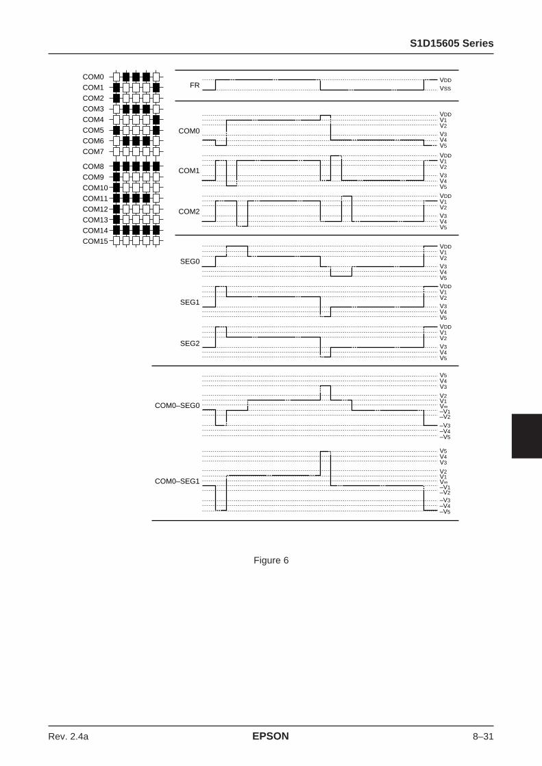
The Liquid Crystal Driver CircuitsThese are a 197-channel (S1D15605 Series), a 181-channel (S1D15606 Series) multiplexers 165-channel(S1D15607 Series), 187-channel (S1D15608 Series)and a 185-channel (S1D15609 Series) that generatefour voltage levels for driving the liquid crystal. Thecombination of the display data, the COM scan signal,and the FR signal produces the liquid crystal drivevoltage output.Figure 6 shows examples of the SEG and COM outputwave form.
Table 6
Status COM Scan DirectionS1D15605***** S1D15606***** S1D15607***** S1D15608***** S1D15609*****
Normal COM0 → COM63 COM0 → COM47 COM0 → COM31 COM0 → COM53 COM0 → COM51Reverse COM63 → COM0 COM47 → COM0 COM31 → COM0 COM53 → COM0 COM51 → COM0
S1D15605 Series
Rev. 2.4a EPSON 8–31
Figure 6
COM0
COM1
COM2
COM3
COM4
COM5
COM6
COM7
FR
COM0
COM1
COM2
SEG0
SEG1
SEG2
COM0–SEG0
COM0–SEG1
COM8
COM9
COM10
COM11
COM12
COM13
COM14
COM15
VDDV1V2
V3V4V5
VDDV1V2
V3V4V5
VDDV1V2
V3V4V5
VDDV1V2
V5V4V3
–V3–V4–V5
V2V1V∞–V1–V2
V5V4V3
–V3–V4–V5
V2V1V∞–V1–V2
V3V4V5
VDDV1V2
V3V4V5
VDDV1V2
V3V4V5
VDD
VSS

S1D15605 Series
8–32 EPSON Rev. 2.4a
The Power Supply CircuitsThe power supply circuits are low-power consumptionpower supply circuits that generate the voltage levelsrequired for the liquid crystal drivers. They compriseBooster circuits, voltage regulator circuits, and voltagefollower circuits. They are only enabled in master
operation.The power supply circuits can turn the Booster circuits,the voltage regulator circuits, and the voltage followercircuits ON of OFF independently through the use of thePower Control Set command. Consequently, it is possibleto make an external power supply and the internalpower supply function somewhat in parallel. Table 7shows the Power Control Set Command 3-bit datacontrol function, and Table 8 shows referencecombinations.
Table 7 The Control Details of Each Bit of the Power Control Set Command
ItemStatus
“1” “0”D2 Booster circuit control bit ON OFFD1 Voltage regulator circuit (V regulator circuit) control bit ON OFFD0 Voltage follower circuit (V/F circuit) control bit ON OFF
Table 8 Reference Combinations
V ExternalStep-up
Use Settings D2 D1 D0Step-up
regulatorV/F
voltagevoltage
circuitcircuit
circuitinput
systemterminal
1 Only the internal power supply is 1 1 1 O O O VSS2 Usedused
2 Only the V regulator circuit and 0 1 1 X O O VOUT, VSS2 Openthe V/F circuit are used
3 Only the V/F circuit is used 0 0 1 X X O V5, VSS2 Open4 Only the external power supply is 0 0 0 X X X V1 to V5 Open
used
* The “step-up system terminals” refer CAP1+, CAP1–, CAP2+, CAP2–, and CAP3–.* While other combinations, not shown above, are also possible, these combinations are not recommended
because they have no practical use.
The Step-up Voltage Circuits
Using the step-up voltage circuits equipped within theS1D15605 Series chips it is possible to product a Quadstep-up, a Triple step-up, and a Double step-up of theVDD – VSS2 voltage levels.Quad step-up: Connect capacitor C1 between CAP1+
and CAP1–, between CAP2+ and CAP2–,between CAP1+ and CAP3–, and betweenVSS2 and VOUT, to produce a voltage levelin the negative direction at the VOUT
terminal that is 4 times the voltage levelbetween VDD and VSS2.
Triple step-up: Connect capacitor C1 between CAP1+and CAP1–, between CAP2+ and CAP2–and between VSS2 and VOUT, and shortbetween CAP3– and VOUT to produce avoltage level in the negative direction at theVOUT terminal that is 3 times the voltage
difference between VDD and VSS2.Double step-up: Connect capacitor C1 between
CAP1+ and CAP1–, and between VSS2 andVOUT, leave CAP2+ open, and shortbetween CAP2–, CAP3– and VOUT toproduce a voltage in the negative directionat the VOUT terminal that is twice the voltagebetween VDD and VSS2.
The step-up voltage relationships are shown in Figure 7.

S1D15605 Series
Rev. 2.4a EPSON 8–33
VSS2
VOUT
CAP3–
CAP1+
CAP1–
CAP2–
CAP2+
C1
C1
C1
C1
+
+
+
S1D
1560
5 S
erie
s
4 x step-up voltage circuit 3 x step-up voltage circuit 2 x step-up voltage circuit
VSS2
VOUT
CAP3–
CAP1+
CAP1–
CAP2–
CAP2+
C1
C1
C1
+
+
+
S1D
1560
5 S
erie
s
VSS2
VOUT
CAP3–
CAP1+
CAP1–
CAP2–
CAP2+OPEN
C1
C1
+
+
S1D
1560
5 S
erie
s
VDD = 0V
VSS2 = –3V
VOUT = 4 x VSS2 = –12V
4x step-up voltage relationships
VDD = 0V
VSS2 = –3V
VOUT = 3 x VSS2 = –9V
3x step-up voltage relationships
VDD = 0V
VSS2 = –5V
VOUT = 2 x VSS2 = –10V
2x step-up voltage relationships
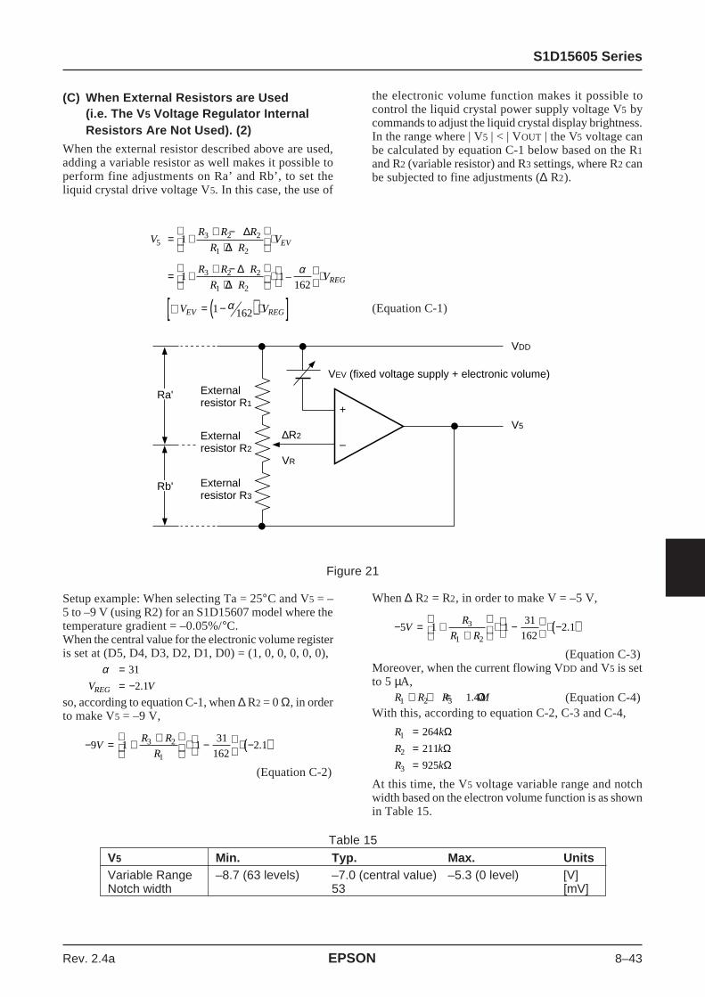
(A) When the V 5 Voltage Regulator InternalResistors Are Used
Through the use of the V5 voltage regulator internalresistors and the electronic volume function the liquidcrystal power supply voltage V5 can be controlled bycommands alone (without adding any external resistors),making it possible to adjust the liquid crystal displaybrightness. The V5 voltage can be calculated usingequation A-1 over the range where | V5 | < | VOUT |.
The Voltage Regulator Circuit
The step-up voltage generated at VOUT outputs theliquid crystal driver voltage V5 through the voltageregulator circuit.Because the S1D15605 Series chips have an internalhigh-accuracy fixed voltage power supply with a 64-level electronic volume function and internal resistorsfor the V5 voltage regulator, systems can be constructedwithout having to include high-accuracy voltageregulator circuit components.Moreover, in the S1D15605 Series, three types of thermalgradients have been prepared as VREG options: (1)approximately -0.05%/°C (2) approximately -0.2%/°C,and (3) external input (supplied to the VRS terminal).
Figure 7
* The VSS2 voltage range must be set so that the VOUT terminal voltage does not exceed the absolute maximum ratedvalue.

S1D15605 Series
8–34 EPSON Rev. 2.4a
Figure 8
Rb/Ra is the V5 voltage regulator internal resistor ratio,and can be set to 8 different levels through the V5
voltage regulator internal resistor ratio set command.The (1 + Rb/Ra) ratio assumes the values shown inTable 11 depending on the 3-bit data settings in the V5
voltage regulator internal resistor ratio register.
α is set to 1 level of 64 possible levels by the electronicvolume function depending on the data set in the 6-bitelectronic volume register. Table 10 shows the value forα depending on the electronic volume register settings.
Table 9Equipment Type Thermal Gradient Units VREG Units
(1) Internal Power Supply –0.05 [%/°C ] –2.1 [V](2) Internal Power Supply –0.2 [%/°C ] –4.9 [V](3) External Input — — VRS [V]
Table 10D5 D4 D3 D2 D1 D0 α0 0 0 0 0 0 630 0 0 0 0 1 620 0 0 0 1 0 61
. .
. .. .1 1 1 1 0 1 21 1 1 1 1 0 11 1 1 1 1 1 0
VEV (constant voltage supply + electronic volume)
Internal Ra+
–
Internal Rb
VDD
V5
(Equation A-1)
VREG is the IC-internal fixed voltage supply, and itsvoltage at Ta = 25°C is as shown in Table 9.
VRb
RaV
Rb
RaV
V V
EV
REG
EV REG
5 1
1 1162
1 162
= +
⋅
= +
⋅
⋅
= −( ) ⋅[ ]–
α
αQ
∴

S1D15605 Series
Rev. 2.4a EPSON 8–35
Table 11
S1D15605***** S1D15606*****Register Equipment Type by Thermal Gradient [Units: %/ °C ] Equipment Type by Thermal Gradient [Units: %/ °C ]
D2 D1 D0 (1) –0.05 (2) –0.2 (3) VREG External Input (1) –0.05 (2) –0.2 (3) VREG External Input0 0 0 3.0 1.3 1.5 3.0 1.3 1.50 0 1 3.5 1.5 2.0 3.5 1.5 2.00 1 0 4.0 1.8 2.5 4.0 1.8 2.50 1 1 4.5 2.0 3.0 4.5 2.0 3.01 0 0 5.0 2.3 3.5 5.0 2.3 3.51 0 1 5.5 2.5 4.0 5.4 2.5 4.01 1 0 6.0 2.8 4.5 5.9 2.8 4.51 1 1 6.4 3.0 5.0 6.4 3.0 5.0
V5 voltage regulator internal resistance ratio registervalue and (1 + Rb/Ra) ratio (Reference value)
For the internal resistance ratio, a manufacturingdispersion of up to ±7% should be taken into account.When not within the tolerance, adjust the V5 voltage byexternally mounting Ra and Rb.Figs. 9, 10, 11 (for S1D15605 Series), 12, 13, 14 (forS1D15606 Series), 15, 16, 17 (for S1D15607 Series), 18( for S1D15608D00B* ) and F igs. 19 ( forS1D15609D00B* ) show V5 voltage measured by valuesof the internal resistance ratio resistor for V5 voltageadjustment and electric volume resister for eachtemperature grade model, when Ta = 25 °C.
S1D15607***** S1D15608*****/S1D15609*****Register Equipment Type by Thermal Gradient [Units: %/ °C ] Equipment Type by Thermal Gradient [Units: %/ °C ]
D2 D1 D0 (1) –0.05 (2) –0.2 (3) VREG External Input –0.05
0 0 0 3.0 1.3 1.5 30 0 1 3.5 1.5 2.0 3.50 1 0 4.0 1.8 2.5 40 1 1 4.5 2.0 3.0 4.51 0 0 5.0 2.3 3.5 51 0 1 5.4 2.5 4.0 5.41 1 0 5.9 2.8 4.5 5.91 1 1 6.4 3.0 5.0 6.4

S1D15605 Series
8–36 EPSON Rev. 2.4a
S1D15605D00B*/S1D15605D11B*
Figure 9: S1D15605D00B*/S1D15605D11B* (1) For Models Where the Thermal Gradient = -0.05%/°C
The V5 voltage as a function of the V5 voltage regulator internal resistor ratio register and the electronicvolume register.
S1D15605D01B*
Figure 10: S1D15605D01B* (2) For Models Where the Thermal Gradient = -0.2%/°C
The V5 voltage as a function of the V5 voltage regulator internal resistor ratio register and the electronicvolume register.
–16
–15
–14
–13
–12
–11
–10
–9
–8
–7
–6
–5
–4
–3
–2
–1
0
V5
[v]
00H
18H
30H
3FHElectric Volume
Resister
1 1 1
0 0 0
0 0 1
0 1 0
0 1 1
1 0 0
1 0 1
1 1 0
The V5 voltage regulator internal resistance ratio
registers(D2, D1, D0)
–16
–15
–14
–13
–12
–11
–10
–9
–8
–7
–6
–5
–4
–3
–2
–1
0
V5
[v]
00H
18H
30H
3FHElectric Volume
Resister
The V5 voltage regulator internal resistance ratio
registers(D2, D1, D0)
1 1 1
0 0 0
0 0 1
0 1 0
0 1 1
1 0 0
1 0 1
1 1 0

S1D15605 Series
Rev. 2.4a EPSON 8–37
S1D15605D02B*
Figure 11: S1D15605D02B* (3) For models with External Input
The V5 voltage as a function of the V5 voltage regulator internal resistor ratio register and the electronicvolume register.
S1D15606D00B*/S1D15606D11B*
Figure 12: S1D15606D00B*/S1D15606D11B* (1) For Models Where the Thermal Gradient = -0.05%/°C
The V5 voltage as a function of the V5 voltage regulator internal resistor ratio register and the electronicvolume register.
–16
–15
–14
–13
–12
–11
–10
–9
–8
–7
–6
–5
–4
–3
–2
–1
0
V5
[v]
00H
18H
30H
3FHElectric Volume
Resister
The V5 voltage regulator internal resistance ratio
registers(D2, D1, D0)
1 1 1
0 0 0
0 0 1
0 1 0
0 1 1
1 0 0
1 0 1
1 1 0
–16
–15
–14
–13
–12
–11
–10
–9
–8
–7
–6
–5
–4
–3
–2
–1
0
V5
[v]
00H
18H
30H
3FHElectric Volume
Resister
The V5 voltage regulator internal resistance ratio
registers(D2, D1, D0)
1 1 1
0 0 0
0 0 1
0 1 0
0 1 1
1 0 0
1 0 1
1 1 0

S1D15605 Series
8–38 EPSON Rev. 2.4a
S1D15606D01B*
Figure 13: S1D15606D01B* (2) For Models Where the Thermal Gradient = -0.2%/°C
The V5 voltage as a function of the V5 voltage regulator internal resistor ratio register and the electronicvolume register.
S1D15606D02B*
Figure 14: S1D15606D02B* (3) For models with External Input
The V5 voltage as a function of the V5 voltage regulator internal resistor ratio register and the electronicvolume register.
–16
–15
–14
–13
–12
–11
–10
–9
–8
–7
–6
–5
–4
–3
–2
–1
0
V5
[v]
00H
18H
30H
3FHElectric Volume
Resister
The V5 voltage regulator internal resistance ratio
registers(D2, D1, D0)
1 1 1
0 0 0
0 0 1
0 1 0
0 1 1
1 0 0
1 0 1
1 1 0
–16
–15
–14
–13
–12
–11
–10
–9
–8
–7
–6
–5
–4
–3
–2
–1
0
V5
[v]
00H
18H
30H
3FHElectric Volume
Resister
The V5 voltage regulator internal resistance ratio
registers(D2, D1, D0)
1 1 1
0 0 0
0 0 1
0 1 0
0 1 1
1 0 0
1 0 1
1 1 0

S1D15605 Series
Rev. 2.4a EPSON 8–39
S1D15607D00B*/S1D15607D11B*
Figure 15: S1D15607D00B*/S1D15607D11B* (1) For Models Where the Thermal Gradient = -0.05%/°C
The V5 voltage as a function of the V5 voltage regulator internal resistor ratio register and the electronicvolume register.
S1D15607D01B*
Figure 16: S1D15607D01B* (2) For Models Where the Thermal Gradient = -0.2%/°C
The V5 voltage as a function of the V5 voltage regulator internal resistor ratio register and the electronicvolume register.
–16
–15
–14
–13
–12
–11
–10
–9
–8
–7
–6
–5
–4
–3
–2
–1
0
V5
[v]
00H
18H
30H
3FHElectric Volume
Resister
The V5 voltage regulator internal resistance ratio
registers(D2, D1, D0)
1 1 1
0 0 0
0 0 1
0 1 0
0 1 1
1 0 0
1 0 1
1 1 0
–16
–15
–14
–13
–12
–11
–10
–9
–8
–7
–6
–5
–4
–3
–2
–1
0
V5
[v]
00H
18H
30H
3FHElectric Volume
Resister
The V5 voltage regulator internal resistance ratio
registers(D2, D1, D0)
1 1 1
0 0 0
0 0 1
0 1 0
0 1 1
1 0 0
1 0 1
1 1 0

S1D15605 Series
8–40 EPSON Rev. 2.4a
S1D15607D02B*
Figure 17: S1D15607D02B* (3) For models with External Input
The V5 voltage as a function of the V5 voltage regulator internal resistor ratio register and the electronicvolume register.
S1D15608D00B*
Figure 18: S1D15608D00B* (1) For Models Where the Thermal Gradient = –0.05%/°C
The V5 voltage as a function of the V5 voltage regulator internal resistor ratio register and the electronicvolume register.
–16
–15
–14
–13
–12
–11
–10
–9
–8
–7
–6
–5
–4
–3
–2
–1
0
V5
[v]
00H
18H
30H
3FHElectric Volume
Resister
The V5 voltage regulator internal resistance ratio
registers(D2, D1, D0)
1 1 1
0 0 0
0 0 1
0 1 0
0 1 1
1 0 0
1 0 1
1 1 0
–16
–15
–14
–13
–12
–11
–10
–9
–8
–7
–6
–5
–4
–3
–2
–1
0
V5
[v]
00H
18H
30H
3FHElectric Volume
Resister
1 1 1
0 0 0
0 0 1
0 1 0
0 1 1
1 0 0
1 0 1
1 1 0
The V5 voltage regulator internal resistance ratio
registers(D2, D1, D0)

S1D15605 Series
Rev. 2.4a EPSON 8–41
S1D15609D00B*
Figure 19: S1D15609D00B* Temperature Gradient = –0.05%/°C Model
The V5 voltage as a function of the V5 voltage regulator internal resistor ratio register and the electronicvolume register.
–16
–15
–14
–13
–12
–11
–10
–9
–8
–7
–6
–5
–4
–3
–2
–1
0
V5
[v]
00H
18H
30H
3FHElectric Volume
Resister
The V5 voltage regulator internal resistance ratio
registers(D2, D1, D0)
1 1 1
0 0 0
0 0 1
0 1 0
0 1 1
1 0 0
1 0 1
1 1 0
Setup example: When selecting Ta = 25°C and V5 = 7V for an S1D15607 model on which Temperaturegradient = –0.05%/°C.Using Figure 15 and the equation A-1, the followingsetup is enabled.
At this time, the variable range and the notch width ofthe V5 voltage is, as shown Table 13, as dependent onthe electronic volume.
Table 12
ContentsRegister
D5 D4 D3 D2 D1 D0For V5 voltage — — — 0 1 0regulatorElectronic Volume 1 0 0 1 0 1
Table 13V5 Min. Typ. Max. UnitsVariable Range –8.4 (63 levels) –6.8 (central value) –5.1 (0 level) [V]Notch width 51 [mV]

S1D15605 Series
8–42 EPSON Rev. 2.4a
VRb
RaV
Rb
RaV
V V
EV
REG
EV REG
5 1
1 1162
1 162
= +
⋅
= +
⋅
⋅
= −( ) ⋅[ ]
'
'
'
'–
α
αQ ( Equation B-1)
Figure 20
∴
VEV (fixed voltage power supply + electronic volume)
External resistor Ra' +
–
External resistor Rb'
VDD
V5
(B) When an External Resistance is Used(i.e., The V5 Voltage Regulator InternalResistors Are Not Used) (1)
The liquid crystal power supply voltage V5 can also beset without using the V5 voltage regulator internalresistors (IRS terminal = LOW) by adding resistors Ra’and Rb’ between VDD and VR, and between VR and V5,
respectively. When this is done, the use of the electronicvolume function makes it possible to adjust the brightnessof the liquid crystal display by controlling the liquidcrystal power supply voltage V5 through commands.In the range where | V5 | < | VOUT |, the V5 voltage canbe calculated using equation B-1 based on the externalresistances Ra’ and Rb’.
Setup example: When selecting Ta = 25°C and V5 = –7 V for an S1D15607 Series model where the temperaturegradient = –0.05%/°C.When the central value of the electron volume registeris (D5, D4, D3, D2, D1, D0) = (1, 0, 0, 0, 0, 0), then α= 31 and VREG = –2.1 V so, according to equation B-1,
VRb
RaV
VRb
Ra
REG5 1 1162
11 1 131
1622 1
= +
⋅ −
⋅
− = +
⋅ −
⋅ −( )
'
'
'
'.
α
(Equation B-2)
Moreover, when the value of the current running throughRa’ and Rb’ is set to 5 µA,
Ra Rb M' ' .+ = 1 4 Ω (Equation B-3)
Consequently, by equations B-2 and B-3,
Rb
RaRa k
Rb k
'
'.
'
'
=
= Ω= Ω
3 12
340
1060
At this time, the V5 voltage variable range and notchwidth, based on the electron volume function, is asgiven in Table 14.
Table 14
V5 Min. Typ. Max. UnitsVariable Range –8.6 (63 levels) –7.0 (central value) –5.3 (0 level) [V]Notch width 52 [mV]
S1D15605 Series
Rev. 2.4a EPSON 8–43
VR R R
R RV
R R R
R RV
V V
EV
REG
EV REG
53 2 2
1 2
3 2 2
1 2
1
1 1162
1 162
= ++ −
+ ∆
⋅
= ++ − ∆
+ ∆
⋅
⋅
= −( ) ⋅[ ]
∆
–α
αQ (Equation C-1)
Figure 21
∴
VEV (fixed voltage supply + electronic volume)
External resistor R1
∆R2External resistor R2
VR
External resistor R3
+
–
VDD
V5
Rb'
Ra'
(C) When External Resistors are Used(i.e. The V 5 Voltage Regulator InternalResistors Are Not Used). (2)
When the external resistor described above are used,adding a variable resistor as well makes it possible toperform fine adjustments on Ra’ and Rb’, to set theliquid crystal drive voltage V5. In this case, the use of
the electronic volume function makes it possible tocontrol the liquid crystal power supply voltage V5 bycommands to adjust the liquid crystal display brightness.In the range where | V5 | < | VOUT | the V5 voltage canbe calculated by equation C-1 below based on the R1
and R2 (variable resistor) and R3 settings, where R2 canbe subjected to fine adjustments (∆ R2).
Setup example: When selecting Ta = 25°C and V5 = –5 to –9 V (using R2) for an S1D15607 model where thetemperature gradient = –0.05%/°C.When the central value for the electronic volume registeris set at (D5, D4, D3, D2, D1, D0) = (1, 0, 0, 0, 0, 0),
α == −
31
2 1V VREG .
so, according to equation C-1, when ∆ R2 = 0 Ω, in orderto make V5 = –9 V,
− = + +
⋅ −
⋅ −( )9 1 1
31
1622 13 2
1V
R R
R.
(Equation C-2)
When ∆ R2 = R2, in order to make V = –5 V,
− = ++
⋅ −
⋅ −( )5 1 1
31
1622 13
1 2V
R
R R.
(Equation C-3)Moreover, when the current flowing VDD and V5 is setto 5 µA,
R R R M1 2 3 1 4+ + = Ω. (Equation C-4)With this, according to equation C-2, C-3 and C-4,
R k
R k
R k
1
2
3
264
211
925
= Ω= Ω= Ω
At this time, the V5 voltage variable range and notchwidth based on the electron volume function is as shownin Table 15.
Table 15
V5 Min. Typ. Max. UnitsVariable Range –8.7 (63 levels) –7.0 (central value) –5.3 (0 level) [V]Notch width 53 [mV]
S1D15605 Series
8–44 EPSON Rev. 2.4a
Sequence
Step1
Step2
End
Details(Command, status)
Display OFF
Display all points ON
Internal power supply OFF
Command addressD7
1
1
D6
0
0
D5
1
1
D4
0
0
Power saver commands(compound)
D3
1
0
D2
1
1
D1
1
0
D0
0
1
High Power Mode
The power supply circuit equipped in the S1D15605Series chips has very low power consumption (normalmode: HPM = HIGH). However, for LCDs or panelswith large loads, this low-power power supply maycause display quality to degrade. When this occurs,setting the HPM terminal to LOW (high power mode)can improve the quality of the display. We recommendthat the display be checked on actual equipment todetermine whether or not to use this mode.Moreover, if the improvement to the display is inadequateeven after high power mode has been set, then it isnecessary to add a liquid crystal drive power supplyexternally.
The Internal Power Supply ShutdownCommand Sequence
The sequence shown in Figure 22 is recommended forshutting down the internal power supply, first placingthe power supply in power saver mode and then turningthe power supply OFF.
* When the V5 voltage regulator internal resistors orthe electronic volume function is used, it is necessaryto at least set the voltage regulator circuit and thevoltage follower circuit to an operating mode usingthe power control set commands. Moreover, it isnecessary to provide a voltage from VOUT when theBooster circuit is OFF.
* The VR terminal is enabled only when the V5 voltageregulator internal resistors are not uesd (i.e. the IRSterminal = LOW). When the V5 voltage regulatorinternal resistors are uesd (i.e. when the IRS terminal= HIGH), then the VR terminal is left open.
* Because the input impedance of the VR terminal ishigh, it is necessary to take into consideration shortleads, shield cables, etc. to handle noise.
The Liquid Crystal Voltage Generator Circuit
The V5 voltage is produced by a resistive voltagedivider within the IC, and can be produced at the V1, V2,V3, and V4 voltage levels required for liquid crystaldriving. Moreover, when the voltage follower changesthe impedance, it provides V1, V2, V3 and V4 to theliquid crystal drive circuit. 1/9 bias or 1/7 bias forS1D15605 Series, 1/8 bias or 1/6 bias for S1D15606Series, 1/6 bias or 1/5 bias for the S1D15607 Series, 1/8 bias or 1/6 bias for S1D15608 Series and 1/8 bias or1/6 bias for S1D15609 Series can be selected.
Figure 22

S1D15605 Series
Rev. 2.4a EPSON 8–45
VDD VDD
VDD
VSS
C1
VSS2
VOUT
CAP3–CAP1+CAP1–CAP2+CAP2–V5
VR
VDD
V1
V2
V3
V4
V5
IRS M/S
C1
C1
C1
C2
C2
C2
C2
C2
S1D
1560
5 S
erie
s
VDD
VSS
C1
VSS2
VOUT
CAP3–CAP1+CAP1–CAP2+CAP2–V5
VR
VDD
V1
V2
V3
V4
V5
IRS M/S
C1
C1
C1
R3
R2
R1
C2
C2
C2
C2
C2
S1D
1560
5 S
erie
s
(1) When the voltage regulator internal resistor is used. (Example where VSS2 = VSS, with 4x step-up)
(2) When the voltage regulator internal resistor is not used. (Example where VSS2 = VSS, with 4x step-up)
➀ When used all of the step-up circuit, voltage regulating circuit and V/F circuit
VDD
VDD
VSSExternalpowersupply
VSS2
VOUT
CAP3–CAP1+CAP1–CAP2+CAP2–V5
VR
VDD
V1
V2
V3
V4
V5
IRS M/S
C2
C2
C2
C2
C2
S1D
1560
5 S
erie
s
VDD
VDD
VSS
VSS2
VOUT
CAP3–CAP1+CAP1–CAP2+CAP2–V5
VR
VDD
V1
V2
V3
V4
V5
IRS M/S
R3
R2
R1
C2
C2
C2
C2
C2
S1D
1560
5 S
erie
s
➁ When the voltage regulator circuit and V/F circuit alone are used(1) When the V5 voltage regulator internal resistor is not used.
(2) When the V5 voltage regulator internal resistor is used.
Externalpowersupply
Reference Circuit Examples
Figure 22 shows reference circuit examples.

S1D15605 Series
8–46 EPSON Rev. 2.4a
Figure 23
* 1 Because the VR terminal input impedance is high, use short leads and shielded lines.* 2 C1 and C2 are determined by the size of the LCD being driven. Select a value that will stabilize the liquid crystal
drive voltage.Example of the Process by which to Determine the Settings:• Turn the voltage regulator circuit and voltage follower circuit ON and supply a voltage to VOUT from the outside.• Determine C2 by displaying an LCD pattern with a heavy load (such as horizontal stripes) and selecting a C2 that
stabilizes the liquid crystal drive voltages (V1 to V5). Note that all C2 capacitors must have the same capacitancevalue.
• Next turn all the power supplies ON and determine C1.
VDD
VDD
Externalpowersupply
VSS
VSS2
VOUT
CAP3–CAP1+CAP1–CAP2+CAP2–V5
VR
VDD
V1
V2
V3
V4
V5
IRS M/S
S1D
1560
5 S
erie
s
➃ When the built-in power is not used
VDD
VDD
VSSExternalpowersupply
VSS2
VOUT
CAP3–CAP1+CAP1–CAP2+CAP2–V5
VR
VDD
V1
V2
V3
V4
V5
IRS M/S
C2
C2
C2
C2
C2
S1D
1560
5 S
erie
s
➂ When the V/F circuit alone is used
Examples of shared reference settingsWhen V5 can vary between –8 and 12 V
Item Set value Units
C1 1.0 to 4.7 µFC2 0.01 to 1.0 µF
VDD, V0
V1
V2
V3
V4
V5
R4
R4
R4
R4
C2
S1D
1560
5 S
erie
s
Reference set value R4: 100kΩ ~ 1MΩIt is recommended to set an optimumresistance value R4 taking the liquid crystaldisplay and the drive waveform.
5 When the built-in power circuit is used to drive aliquid crystal panel heavily loaded with AC or DC, itis recommended to connect an external resistor tostabilize potentials of V1, V2, V3 and V4 which areoutput from the built-in voltage follower.

S1D15605 Series
Rev. 2.4a EPSON 8–47
* Precautions when installing the COG
When installing the COG, it is necessary to duly considerthe fact that there exists a resistance of the ITO wiringoccurring between the driver chip and the externallyconnected parts (such as capacitors and resistors). By theinfluence of this resistance, non-conformity may occurwith the indications on the liquid crystal display.Therefore, when installing the COG design the modulepaying sufficient considerations to the following threepoints.1. Suppress the resistance occurring between the driver
chip pin to the externally connected parts as much aspossible.
2. Suppress the resistance connecting to the powersupply pin of the driver chip.
3. Make various COG module samples with differentITO sheet resistance to select the module with thesheet resistance with sufficient operation margin.
Also, as for this driver IC, pay sufficient attention to thefollowing points when connecting to external parts forthe characteristics of the circuit.1. Connection to the boosting capacitors The boosting
capacitors (the capacitors connecting to respectiveCAP pins and capacitor being inserted betweenVOUT and VSS2) of this IC are being switched overby use of the transistor with very low ON-resistanceof about 10Ω. However, when installing the COG,
Exemplary connection diagram 1. Exemplary connection diagram 2.
the resistance of ITO wiring is being inserted inseries with the switching transistor, thus dominatingthe boosting ability.Consequently, the boosting ability will be hinderedas a result and pay sufficient attention to the wiringto respective boosting capacitors.
2. Connection of the smoothing capacitors for theliquid crystal driveThe smoothing capacitors for the liquid crystaldriving potentials (V1. V2, V3 and V4) areindispensable for liquid crystal drives not only forthe purpose of mere stabilization of the voltagelevels. If the ITO wiring resistance which occurspursuant to installation of the COG is supplementedto these smoothing capacitors, the liquid crystaldriving potentials become unstable to cause non-conformity with the indications of the liquid crystaldisplay. Therefore, when using the COG module,we definitely recommend to connect reinforcingresistors externally.Reference value of the resistance is 100kΩ to 1MΩ.Meanwhile, because of the existence of thesereinforcing resistors, current consumption willincrease.
Indicated below is an exemplary connection diagram ofexternal resistors.Please make sufficient evaluation work for the displaystatuses with any connection tests.
VDD
VDD
V1
V2
V3
V4
V5
R4
R4
R4
R4
C2
C2
S1D
1560
5 S
erie
s
C2
C2
C2
VDD
VDD
V1
V2
V3
V4
V5
R4
R4
C2
C2
S1D
1560
5 S
erie
s
C2
C2
C2

S1D15605 Series
8–48 EPSON Rev. 2.4a
The Reset CircuitWhen the RES input comes to the LOW level, theseLSIs return to the default state. Their default states areas follows:1. Display OFF2. Normal display3. ADC select: Normal (ADC command D0 = LOW)4. Power control register: (D2, D1, D0) = (0, 0, 0)5. Serial interface internal register data clear6. LCD power supply bias rate:
S1D15605***** ........................1/9 biasS1D15606***** , 15608***** , 15609*****................................................................ 1/8 biasS1D15607********* ................1/6 bias
7. All-indicator lamps-on OFF (All-indicator lampsON/OFF command D0 = LOW)
8. Power saving clear9. V5 voltage regulator internal resistors Ra and Rb
separation(In case of S1D15605D11B* , S1D15606D11B* ,S1D15607D11B* , S1D15608D11B* andS1D15609D11B* , internal resistors are connectedwhile RES is LOW.)
10. Output conditions of SEG and COM terminalsSEG : V2/V3, COM : V1/V4
(In case of S1D15605D11B* , S1D15606D11B* ,S1D15607D11B* , S1D15608D11B* andS1D15609D11B* , both the SEG terminal and theCOM terminal output the VDA level while RES isLOW. In case of other models, the SEG terminaloutputs V2 and the COM terminal outputs V1 whileRES is LOW.)
11. Read modify write OFF12. Static indicator OFF
Static indicator register : (D1, D2) = (0, 0)13. Display start line set to first line14. Column address set to Address 015. Page address set to Page 016. Common output status normal17. V5 voltage regulator internal resistor ratio set mode
clear18. Electronic volume register set mode clear
Electronic volume register : (D5, D4, D3, D2, D1,D0) = (1, 0. 0, 0, 0, 0)
19. Test mode clear
On the other hand, when the reset command is used, theabove default settings from 11 to 19 are only executed.
When the power is turned on, the IC internal statebecomes unstable, and it is necessary to initialize itusing the RES terminal. After the initialization, eachinput terminal should be controlled normally.Moreover, when the control signal from the MPU is inthe high impedance, an overcurrent may flow to the IC.After applying a current, it is necessary to take propermeasures to prevent the input terminal from getting intothe high impedance state.If the internal liquid crystal power supply circuit is notused on S1D15605D11B* , S1D15606D11B* ,S1D15607D11B* , S1D15608D11B* andS1D15609D11B* , it is necessary that RES is HIGHwhen the external liquid crystal power supply is turnedon. This IC has the function to discharge V5 when RESis LOW, and the external power supply short-circuits toVDD when RES is LOW.While RES is LOW, the oscillator and the displaytiming generator stop, and the CL, FR, FRS and DOFterminals are fixed to HIGH. The terminals D0 to D7are not affected. The VDD level is output from the SEGand COM output terminals. This means that an internalresistor is connected between VDD and V5.When the internal liquid crystal power supply circuit isnot used on other models of S1D15605 series, it isnecessary that RE is LOWwhen the external liquidcrystal power supply is turned on.While RES is LOW, the oscillator works but the displaytiming generator stops, and the CL, FR, FRS and DOFterminals are fixed to HIGH. The terminals D0 to D7are not affected.

S1D15605 Series
Rev. 2.4a EPSON 8–49
7. COMMANDSThe S1D15605 Series chips identify the data bus signals by a combination of A0, RD (E), WR (R/W) signals. Commandinterpretation and execution does not depend on the external clock, but rather is performed through internal timing only,and thus the processing is fast enough that normally a busy check is not required.In the 8080 MPU interface, commands are launched by inputting a low pulse to the RD terminal for reading, andinputting a low pulse to the WR terminal for writing. In the 6800 Series MPU interface, the interface is placed in a readmode when an HIGH signal is input to the R/W terminal and placed in a write mode when a LOW signal is input to theR/W terminal and then the command is launched by inputting a high pulse to the E terminal. (See “10. TimingCharacteristics” regarding the timing.) Consequently, the 6800 Series MPU interface is different than the 80x86 SeriesMPU interface in that in the explanation of commands and the display commands the status read and display data readRD (E) becomes “1(H)”. In the explanations below the commands are explained using the 8080 Series MPU interfaceas the example.When the serial interface is selected, the data is input in sequence starting with D7.<Explanation of Commands>
(1) Display ON/OFF
This command turns the display ON and OFF.
When the display OFF command is executed when in the display all points ON mode, power saver mode is entered. Seethe section on the power saver for details.
(2) Display Start Line Set
This command is used to specify the display start line address of the display data RAM shown in Figure 4. For furtherdetails see the explanation of this function in “The Line Address Circuit”.
(3) Page Address Set
This command specifies the page address corresponding to the low address when the MPU accesses the display dataRAM (see Figure 4). Specifying the page address and column address enables to access a desired bit of the display dataRAM. Changing the page address does not accompany a change in the status display. See the page address circuit inthe Function Description (page 1–20) for the detail.
E R/WA0 RD WR D7 D6 D5 D4 D3 D2 D1 D0 Line address0 1 0 0 1 0 0 0 0 0 0 0
0 0 0 0 0 1 10 0 0 0 1 0 2
↓ ↓1 1 1 1 1 0 621 1 1 1 1 1 63
E R/WA0 RD WR D7 D6 D5 D4 D3 D2 D1 D0 Page address0 1 0 1 0 1 1 0 0 0 0 0
0 0 0 1 10 0 1 0 2
↓ ↓0 1 1 1 71 0 0 0 8
E R/WA0 RD WR D7 D6 D5 D4 D3 D2 D1 D0 Setting0 1 0 1 0 1 0 1 1 1 1 Display ON
0 Display OFF

S1D15605 Series
8–50 EPSON Rev. 2.4a
(4) Column Address Set
This command specifies the column address of the display data RAM shown in Figure 4. The column address is splitinto two sections (the higher 4 bits and the lower 4 bits) when it is set (fundamentally, set continuously). Each time thedisplay data RAM is accessed, the column address automatically increments (+1), making it possible for the MPU tocontinuously read from/write to the display data. The column address increment is topped at 83H. This does not changethe page address continuously. See the function explanation in “The Column Address Circuit,” for details.
(5) Status Read
(6) Display Data Write
This command writes 8-bit data to the specified display data RAM address. Since the column address is automaticallyincremented by “1” after the write, the MPU can write the display data.
(7) Display Data Read
This command reads 8-bit data from the specified display data RAM address. Since the column address is automaticallyincremented by “1” after the read, the CPU can continuously read multiple-word data. One dummy read is requiredimmediately after the column address has been set. See the function explanation in “Display Data RAM” for theexplanation of accessing the internal registers. When the serial interface is used, reading of the display data becomesunavailable.
BUSY When BUSY = 1, it indicates that either processing is occurring internally or a reset conditionis in process. While the chip does not accept commands until BUSY = 0, if the cycle time canbe satisfied, there is no need to check for BUSY conditions.
ADC This shows the relationship between the column address and the segment driver.0: Reverse (column address 131-n ↔ SEG n)1: Normal (column address n ↔ SEG n)(The ADC command switches the polarity.)
ON/OFF ON/OFF: indicates the display ON/OFF state.0: Display ON1: Display OFF(This display ON/OFF command switches the polarity.)
RESET This indicates that the chip is in the process of initialization either because of a RES signal orbecause of a reset command.
0: Operating state1: Reset in progress
E R/WA0 RD WR D7 D6 D5 D4 D3 D2 D1 D01 1 0 Write data
E R/WA0 RD WR D7 D6 D5 D4 D3 D2 D1 D01 0 1 Read Data
E R/W ColumnA0 RD WR D7 D6 D5 D4 D3 D2 D1 D0 A7 A6 A5 A4 A3 A2 A1 A0 address0 1 0 0 0 0 1 A7 A6 A5 A4 0 0 0 0 0 0 0 0 0
0 A3 A2 A1 A0 0 0 0 0 0 0 0 1 10 0 0 0 0 0 1 0 2
↓ ↓1 0 0 0 0 0 1 0 1301 0 0 0 0 0 1 1 131
HIGH bits →LOW bits →
E R/WA0 RD WR D7 D6 D5 D4 D3 D2 D1 D00 0 1 BUSY ADC ON/OFF RESET 0 0 0 0

S1D15605 Series
Rev. 2.4a EPSON 8–51
(8) ADC Select (Segment Driver Direction Select)
This command can reverse the correspondence between the display RAM data column address and the segment driveroutput. Thus, sequence of the segment driver output pins may be reversed by the command. See the column addresscircuit (page 1–20) for the detail. Increment of the column address (by “1”) accompanying the reading or writing thedisplay data is done according to the column address indicated in Figure 4.
(9) Display Normal/Reverse
This command can reverse the lit and unlit display without overwriting the contents of the display data RAM. Whenthis is done the display data RAM contents are maintained.
(10) Display All Points ON/OFF
This command makes it possible to force all display points ON regardless of the content of the display data RAM. Thecontents of the display data RAM are maintained when this is done. This command takes priority over the displaynormal/reverse command.
When the display is in an OFF mode, executing the display all points ON command will place the display in power savemode. For details, see the (20) Power Save section.
(11) LCD Bias Set
This command selects the voltage bias ratio required for the liquid crystal display. This command can be valid whilethe V/F circuit of Power Supply circuit is in operation.
(12) Read/Modify/Write
This command is used paired with the “END” command. Once this command has been input, the display data readcommand does not change the column address, but only the display data write command increments (+1) the columnaddress. This mode is maintained until the END command is input. When the END command is input, the columnaddress returns to the address it was at when the read/modify/write command was entered. This function makes itpossible to reduce the load on the MPU when there are repeating data changes in a specified display region, such as whenthere is a blanking cursor.
* Even in read/modify/write mode, other commands aside from display data read/write commands can also be used.However, the column address set command cannot be used.
E R/WA0 RD WR D7 D6 D5 D4 D3 D2 D1 D0 Setting0 1 0 1 0 1 0 0 0 0 0 Normal
1 Reverse
E R/WA0 RD WR D7 D6 D5 D4 D3 D2 D1 D0 Setting0 1 0 1 0 1 0 0 1 1 0 RAM Data HIGH
LCD ON voltage (normal)1 RAM Data LOW
LCD ON voltage (reverse)
E R/WA0 RD WR D7 D6 D5 D4 D3 D2 D1 D0 Setting0 1 0 1 0 1 0 0 1 0 0 Normal display mode
1 Display all points ON
E R/W Select StatusA0 RD WR D7 D6 D5 D4 D3 D2 D1 D0 S1D15605***** S1D15606***** S1D15607***** S1D15608***** S1D15609*****0 1 0 1 0 1 0 0 0 1 0 1/9 bias 1/8 bias 1/6 bias 1/8 bias 1/8 bias
1 1/7 bias 1/6 bias 1/5 bias 1/6 bias 1/6 bias
E R/WA0 RD WR D7 D6 D5 D4 D3 D2 D1 D00 1 0 1 1 1 0 0 0 0 0

S1D15605 Series
8–52 EPSON Rev. 2.4a
• The sequence for cursor display
Figure 24
(13) End
This command releases the read/modify/write mode, and returns the column address to the address it was at when themode was entered.
Figure 25
(14) Reset
This command initializes the display start line, the column address, the page address, the common output mode, the V5
voltage regulator internal resistor ratio, the electronic volume, and the static indicator are reset, and the read/modify/write mode and test mode are released. There is no impact on the display data RAM. See the function explanation in“Reset” for details.The reset operation is performed after the reset command is entered.
The initialization when the power supply is applied must be done through applying a reset signal to the RES terminal.The reset command must not be used instead.
E R/WA0 RD WR D7 D6 D5 D4 D3 D2 D1 D00 1 0 1 1 1 0 1 1 1 0
E R/WA0 RD WR D7 D6 D5 D4 D3 D2 D1 D00 1 0 1 1 1 0 0 0 1 0
Page address set
Column address set
Dummy read
Data read
Data writeData process
End
Yes
NoChange complete?
Read/modify/write
NN+m• • •N+3N+2N+1NColumn address
Read/modify/write mode set End
Return

S1D15605 Series
Rev. 2.4a EPSON 8–53
(15) Common Output Mode Select
This command can select the scan direction of the COM output terminal. For details, see the function explanation in“Common Output Mode Select Circuit.”
(16) Power Controller Set
This command sets the power supply circuit functions. See the function explanation in “The Power Supply Circuit,”for details
(17) V5 Voltage Regulator Internal Resistor Ratio Set
This command sets the V5 voltage regulator internal resistor ratio. For details, see the function explanation is “ThePower Supply Circuits.”
(18) The Electronic Volume (Double Byte Command)
This command makes it possible to adjust the brightness of the liquid crystal display by controlling the liquid crystaldrive voltage V5 through the output from the voltage regulator circuits of the internal liquid crystal power supply.This command is a two byte command used as a pair with the electronic volume mode set command and the electronicvolume register set command, and both commands must be issued one after the other.
• The Electronic Volume Mode Set
When this command is input, the electronic volume register set command becomes enabled. Once the electronic volumemode has been set, no other command except for the electronic volume register command can be used. Once theelectronic volume register set command has been used to set data into the register, then the electronic volume mode isreleased.
E R/WA0 RD WR D7 D6 D5 D4 D3 D2 D1 D0 Selected Mode0 1 0 0 0 1 0 1 0 Booster circuit: OFF
1 Booster circuit: ON
0 Voltage regulator circuit: OFF1 Voltage regulator circuit: ON
0 Voltage follower circuit: OFF1 Voltage follower circuit: ON
[Translator’s Note: the abbreviations explained within these parentheses for Vand V/F have been written out in the English translation and are therefore nolonger necessary.]
E R/WA0 RD WR D7 D6 D5 D4 D3 D2 D1 D0 Rb/Ra Ratio0 1 0 0 0 1 0 0 0 0 0 Small
0 0 10 1 0
↓ ↓1 1 01 1 1 Large
E R/WA0 RD WR D7 D6 D5 D4 D3 D2 D1 D00 1 0 1 0 0 0 0 0 0 1
E R/W Selected ModeA0 RD WR D7 D6 D5 D4 D3 D2 D1 D0 S1D15605***** S1D15606***** S1D15607***** S1D15608***** S1D15609*****0 1 0 1 1 0 0 0 * * * Normal COM0→COM63COM0→COM47 COM0→COM31 COM0→COM53COM0→COM51
1 Reverse COM63→COM0 COM47→COM0 COM31→COM0 COM53→COM0 COM51→COM0
* Disabled bit

S1D15605 Series
8–54 EPSON Rev. 2.4a
• Electronic Volume Register Set
By using this command to set six bits of data to the electronic volume register, the liquid crystal drive voltage V5 assumesone of the 64 voltage levels.When this command is input, the electronic volume mode is released after the electronic volume register has been set.
When the electronic volume function is not used, set this to (1, 0, 0, 0, 0, 0)
• The Electronic Volume Register Set Sequence
Figure 26
(19) Static Indicator (Double Byte Command)
This command controls the static drive system indicator display. The static indicator display is controlled by thiscommand only, and is independent of other display control commands.This is used when one of the static indicator liquid crystal drive electrodes is connected to the FR terminal, and the otheris connected to the FRS terminal. A different pattern is recommended for the static indicator electrodes than for thedynamic drive electrodes. If the pattern is too close, it can result in deterioration of the liquid crystal and of theelectrodes.The static indicator ON command is a double byte command paired with the static indicator register set command, andthus one must execute one after the other. (The static indicator OFF command is a single byte command.)
• Static Indicator ON/OFF
When the static indicator ON command is entered, the static indicator register set command is enabled. Once the staticindicator ON command has been entered, no other command aside from the static indicator register set command canbe used. This mode is cleared when data is set in the register by the static indicator register set command.
E R/WA0 RD WR D7 D6 D5 D4 D3 D2 D1 D0 | V5 |0 1 0 * * 0 0 0 0 0 1 Small0 1 0 * * 0 0 0 0 1 00 1 0 * * 0 0 0 0 1 1
↓ ↓0 1 0 * * 1 1 1 1 1 00 1 0 * * 1 1 1 1 1 1 Large
* Inactive bit
E R/WA0 RD WR D7 D6 D5 D4 D3 D2 D1 D0 Static Indicator0 1 0 1 0 1 0 1 1 0 0 OFF
1 ON
Electronic volume mode set
Electronic volume register set
Electronic volume mode clear
Yes
NoChanges complete?

S1D15605 Series
Rev. 2.4a EPSON 8–55
• Static Indicator Register Set
This command sets two bits of data into the static indicator register, and is used to set the static indicator into a blinkingmode.
• Static Indicator Register Set Sequence
Figure 27
(20) Power Save (Compound Command)
When the display all points ON is performed while the display is in the OFF mode, the power saver mode is entered,thus greatly reducing power consumption.The power saver mode has two different modes: the sleep mode and the standby mode. When the static indicator is OFF,it is the sleep mode that is entered. When the static indicator is ON, it is the standby mode that is entered.In the sleep mode and in the standby mode, the display data is saved as is the operating mode that was in effect beforethe power saver mode was initiated, and the MPU is still able to access the display data RAM.Refer to figure 28 for power save off sequence.
Figure 28
Static indicator OFF
Power saver (compound command)
Static indicator ON
Standby mode
Standby mode cancel
Sleep mode
Sleep mode cancel
Power save OFF (compound command)Display all points OFF command
Static indicator ON(2 bytes command)
Power save OFF(Display all points OFF command)
Static indicator mode set
Static indicator register set
Static indicator mode clear
Yes
NoChanges complete?
E R/WA0 RD WR D7 D6 D5 D4 D3 D2 D1 D0 Indicator Display State0 1 0 * * * * * * 0 0 OFF
0 1 ON (blinking at approximately one second intervals)1 0 ON (blinking at approximately 0.5 second intervals)1 1 ON (constantly on)
* Disabled bit
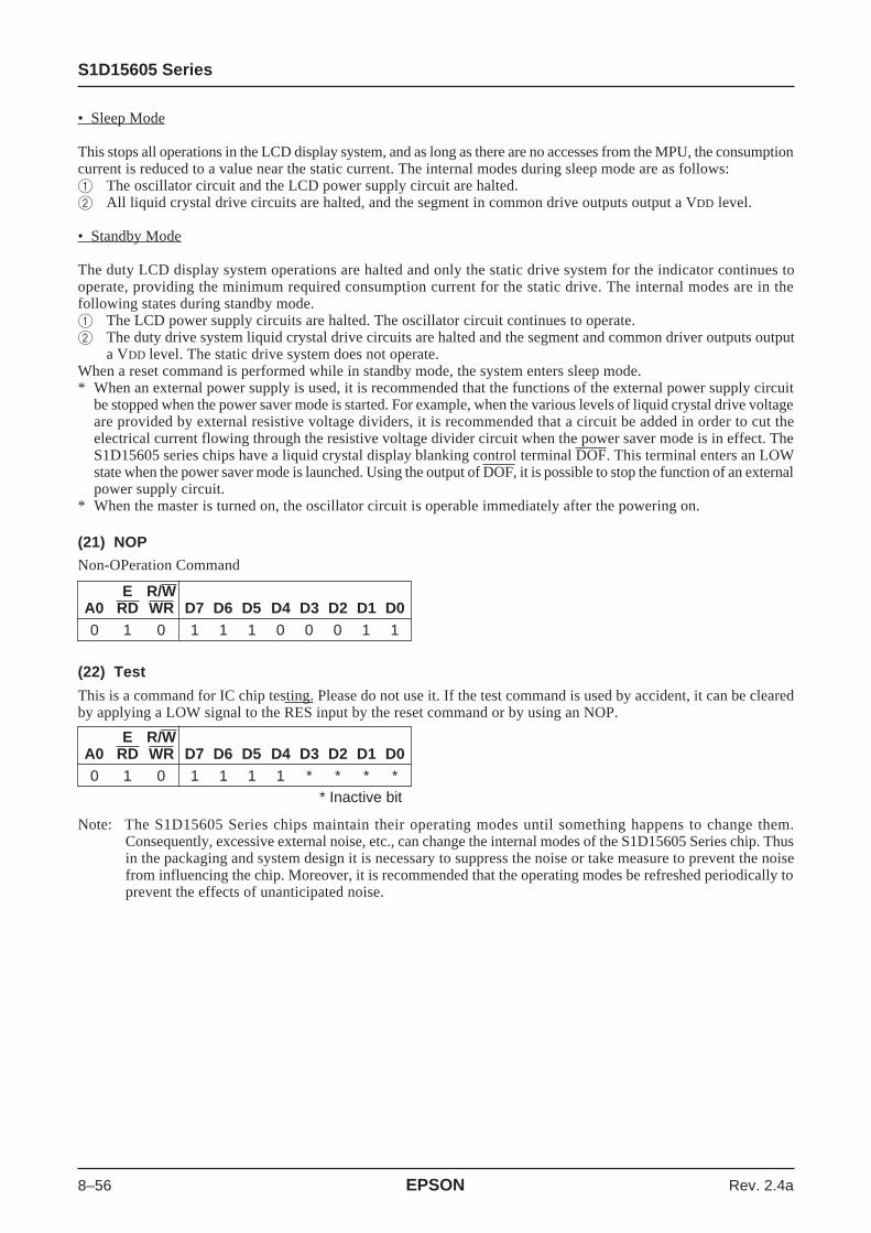
S1D15605 Series
8–56 EPSON Rev. 2.4a
• Sleep Mode
This stops all operations in the LCD display system, and as long as there are no accesses from the MPU, the consumptioncurrent is reduced to a value near the static current. The internal modes during sleep mode are as follows:1 The oscillator circuit and the LCD power supply circuit are halted.2 All liquid crystal drive circuits are halted, and the segment in common drive outputs output a VDD level.
• Standby Mode
The duty LCD display system operations are halted and only the static drive system for the indicator continues tooperate, providing the minimum required consumption current for the static drive. The internal modes are in thefollowing states during standby mode.1 The LCD power supply circuits are halted. The oscillator circuit continues to operate.2 The duty drive system liquid crystal drive circuits are halted and the segment and common driver outputs output
a VDD level. The static drive system does not operate.When a reset command is performed while in standby mode, the system enters sleep mode.* When an external power supply is used, it is recommended that the functions of the external power supply circuit
be stopped when the power saver mode is started. For example, when the various levels of liquid crystal drive voltageare provided by external resistive voltage dividers, it is recommended that a circuit be added in order to cut theelectrical current flowing through the resistive voltage divider circuit when the power saver mode is in effect. TheS1D15605 series chips have a liquid crystal display blanking control terminal DOF. This terminal enters an LOWstate when the power saver mode is launched. Using the output of DOF, it is possible to stop the function of an externalpower supply circuit.
* When the master is turned on, the oscillator circuit is operable immediately after the powering on.
(21) NOP
Non-OPeration Command
(22) Test
This is a command for IC chip testing. Please do not use it. If the test command is used by accident, it can be clearedby applying a LOW signal to the RES input by the reset command or by using an NOP.
Note: The S1D15605 Series chips maintain their operating modes until something happens to change them.Consequently, excessive external noise, etc., can change the internal modes of the S1D15605 Series chip. Thusin the packaging and system design it is necessary to suppress the noise or take measure to prevent the noisefrom influencing the chip. Moreover, it is recommended that the operating modes be refreshed periodically toprevent the effects of unanticipated noise.
E R/WA0 RD WR D7 D6 D5 D4 D3 D2 D1 D00 1 0 1 1 1 1 * * * *
* Inactive bit
E R/WA0 RD WR D7 D6 D5 D4 D3 D2 D1 D00 1 0 1 1 1 0 0 0 1 1

S1D15605 Series
Rev. 2.4a EPSON 8–57
Command Code
Command A0 RD WR D7 D6 D5 D4 D3 D2 D1 D0 Function
(1) Display ON/OFF 0 1 0 1 0 1 0 1 1 1 0 LCD display ON/OFF1 0: OFF, 1: ON
(2) Display start line set 0 1 0 0 1 Display start address Sets the display RAM displaystart line address
(3) Page address set 0 1 0 1 0 1 1 Page address Sets the display RAM pageaddress
(4) Column address 0 1 0 0 0 0 1 Most significant Sets the most significant 4 bitsset upper bit column address of the display RAM column
address.Column address 0 1 0 0 0 0 0 Least significant Sets the least significant 4 bits ofset lower bit column address the display RAM column address.
(5) Status read 0 0 1 Status 0 0 0 0 Reads the status data
(6) Display data write 1 1 0 Write data Writes to the display RAM
(7) Display data read 1 0 1 Read data Reads from the display RAM
(8) ADC select 0 1 0 1 0 1 0 0 0 0 0 Sets the display RAM address1 SEG output correspondence
0: normal, 1: reverse
(9) Display normal/ 0 1 0 1 0 1 0 0 1 1 0 Sets the LCD display normal/reverse 1 reverse
0: normal, 1: reverse
(10) Display all points 0 1 0 1 0 1 0 0 1 0 0 Display all pointsON/OFF 1 0: normal display
1: all points ON
(11) LCD bias set 0 1 0 1 0 1 0 0 0 1 0 Sets the LCD drive voltage1 bias ratio
S1D15605***** .. 0: 1/9, 1: 1/7S1D15606*****/S1D15608*****/S1D15609***** . 0: 1/8, 1: 1/6S1D15607***** .. 0: 1/6, 1: 1/5
(12) Read/modify/write 0 1 0 1 1 1 0 0 0 0 0 Column address incrementAt write: +1At read: 0
(13) End 0 1 0 1 1 1 0 1 1 1 0 Clear read/modify/write
(14) Reset 0 1 0 1 1 1 0 0 0 1 0 Internal reset
(15) Common output 0 1 0 1 1 0 0 0 * * * Select COM output scanmode select 1 direction
0: normal direction,1: reverse direction
(16) Power control set 0 1 0 0 0 1 0 1 Operating Select internal powermode supply operating mode
(17) V5 voltage 0 1 0 0 0 1 0 0 Resistor ratio Select internal resistor ratioregulator internal (Rb/Ra) moderesistor ratio set
(18) Electronic volume 0 1 0 1 0 0 0 0 0 0 1mode setElectronic volume 0 1 0 * * Electronic volume value Set the V5 output voltageregister set electronic volume register
(19) Static indicator 0 1 0 1 0 1 0 1 1 0 0 0: OFF, 1: ONON/OFF 1Static indicator 0 1 0 * * * * * * Mode Set the flashing moderegister set
(20) Power saver Display OFF and display allpoints ON compound command
(21) NOP 0 1 0 1 1 1 0 0 0 1 1 Command for non-operation
(22) Test 0 1 0 1 1 1 1 * * * * Command for IC test. Do notuse this command
(Note) *: disabled data
Table 16 Table of S1D15605 Series Commands

S1D15605 Series
8–58 EPSON Rev. 2.4a
8. COMMAND DESCRIPTIONInstruction Setup: Reference (reference)(1) Initialization
Note: With this IC, when the power is applied, LCD driving non-selective potentials V2 and V3 (SEG pin) and V1and V4 (COM pin) are output through the LCD driving output pins SEG and COM. When electric charge isremaining in the smoothing capacitor connecting between the LCD driving voltage output pins (V1 ~ V5) and theVDD pin, the picture on the display may become totally dark instantaneously when the power is turned on. Toavoid occurrence of such a failure, we recommend the following flow when turning on the power.
1 When the built-in power is being used immediately after turning on the power:
Turn ON the VDD-VSS power keeping the RES pin = LOW.
When the power is stabilized
Initialized state (Default) *1
This concludes the initialization
Function setup by command input (User setup) (11) LCD bias setting *2 (8) ADC selection *3 (15) Common output state selection *4
Function setup by command input (User setup) (17) Setting the built-in resistance radio for regulation of the V5 voltage *5 (18) Electronic volume control *6
Function setup by command input (User setup) (16) Power control setting *7
Release the reset state. (RES pin = HIGH)
(In case of S1D15605D11B*, S1D15606D11B*, S1D15607D11B*, S1D15608D11B* and S1D15609D11B*)Arrange to execute all the procedures from releasing the reset state through setting the power control within 5ms.(In case of other models) execute the procedures from turning on the power to setting the power control in 5ms.
* The target time of 5ms will result to vary depending on the panel characteristics and the capacitance of the smoothingcapacitor. Therefore, we suggest you to conduct an operation check using the actual equipment.
Notes: Refer to respective sections or paragraphs listed below.*1: 6. Description of functions; “Resetting circuit” (If takes not more than 2 ms from Power Supply ON to
the stability of internal oscillating circuit.)*2: 7. Command description; “(11) LCD bias setting”*3: 7. Command description; “(8) ADC selection”*4: 7. Command description; “(15) Common output state selection”*5: 6. Description of functions; “Power circuit” & Command description; “(17) Setting the built-in
resistance radio for regulation of the V5 voltage”*6: 6. Description of functions; “Power circuit” & Command description; “(18) Electronic volume control”*7: 6. Description of functions; “Power circuit” & Command description; “(16) Power control setting”

S1D15605 Series
Rev. 2.4a EPSON 8–59
2 When the built-in power is not being used immediately after turning on the power:
* The target time of 5ms will result to vary depending on the panel characteristics and the capacitance of the smoothingcapacitor. Therefore, we suggest you to conduct an operation check using the actual equipment.
Notes: Refer to respective sections or paragraphs listed below.*1: 6. Description of functions; “Resetting circuit” (The contents of DDRAM can be variable even in the
initial setting (Default) at the reset state.)*2: 7. Command description; “(11) LCD bias setting”*3: 7. Command description; “(8) ADC selection”*4: 7. Command description; “(15) Common output state selection”*5: 6. Description of functions; “Power circuit” & “(17) Command description; Setting the built-in
resistance radio for regulation of the V5 voltage”*6: 6. Description of functions; “Power circuit” & “(18) Command description; Electronic volume control”*7: 6. Description of functions; “Power circuit” & “(16) Command description; Power control setting”*8: 7. The power saver ON state can either be in sleep state or stand-by state.
Command description; “Power saver START (multiple commands)”
Turn ON the VDD-VSS power keeping the RES pin = LOW.
When the power is stabilized
Power saver START (multiple commands) *8
Power saver OFF *8
Initialized state (Default) *1
This concludes the initialization
Function setup by command input (User setup) (11) LCD bias setting *2 (8) ADC selection *3 (15) Common output state selection *4
Function setup by command input (User setup) (17) Setting the built-in resistance radio for regulation of the V5 voltage *5 (18) Electronic volume control *6
Function setup by command input (User setup) (16) Power control setting *7
Release the reset state. (RES pin = HIGH) (In case of S1D15605D11B*, S1D15606D11B*, S1D15607D11B*, S1D15608D11B* and S1D15609D11B*)Arrange to start the power saver within 5ms after releasing the reset state.(In case of other models) execute the procedures from turning on the power to setting the power control in 5ms.
Arrange to start power control setting within 5ms after turning OFF the power saver.

S1D15605 Series
8–60 EPSON Rev. 2.4a
(2) Data Display
(3) Power OFF *14• In case of S1D15605D11B*, S1D15606D11B* , S1D15607D11B*, S1D15608D11B* and S1D15609D11B* ,
• In case of other models,
Notes: Reference items*14: The logic circuit of this IC’s power supply VDD - VSS controls the driver of the LCD power supply
VDD - V5. So, if the power supply VDD - VSS is cut off when the LCD power supply VDD - V5 hasstill any residual voltage, the driver (COM. SEG) may output any uncontrolled voltage. When turningoff the power, observe the following basic procedures:• After turning off the internal power supply, make sure that the potential V5 ~ V1 has become below
the threshold voltage of the LCD panel, and then turn off this IC’s power supply (VDD - VSS).6. Description of Function, 6.7 Power Circuit
*15: After inputting the power save command, be sure to reset the function using the RES terminal until thepower supply VDD - VSS is turned off. 7. Command Description (20) Power Save
*16: After inputting the power save command, do not reset the function using the RES terminal until thepower supply VDD - VSS is turned off. 7. Command Description (20) Power Save
End of data display
End of initialization
Function setup by command input (User setup) (2) Display start line set *9 (3) Page address set *10 (4) Column address set *11
Function setup by command input (User setup) (1) Display ON/OFF *13
Function setup by command input (User setup) (6) Display data write *12
Reset active (RES pin = LOW)
Optional status
Function setup by command input (User setup) (20) Power save *15
VDD – VSS power OFF
Set the time (tL) from reset active to turning off the VDD - VSS power (VDD - VSS = 1.8 V) longer than the time (tH) when the potential of V5 ~ V1 becomes below the threshold voltage (approximately 1 V) of the LCD panel.For tH, refer to the <Reference Data> of this event. When tH is too long, insert a resistor between V5 and VDD to reduce it.
VDD – VSS power OFF
Optional status
Function setup by command input (User setup) (20) Power save *15
Set the time (tL) from power save to turning off the VDD - VSS power (VDD - VSS = 1.8 V) longer than the time (tH) when the potential of V5 ~ V1 becomes below the threshold voltage (approximately 1V) of the LCD panel.• tH is determined depending on the voltage
regulator external resistors Ra and Rb and the time constant of V5 ~ V1 smoothing capacity C2.
• When an internal resistor is used, it is recommended to insert a resistor R between VDD and V5 to reduce tH.
Notes: Reference items*9: Command Description; Display start line set
*10: Command Description; Page address set*11: Command Description; Column address set*12: Command Description; Display data write*13: Command Description; Display ON/OFF
Avoid displaying all the data at the datadisplay start (when the display is ON) inwhite.

S1D15605 Series
Rev. 2.4a EPSON 8–61
(4) Refresh
It is recommended that the operating modes and display contents be refreshed periodically to prevent the effect ofunexpected noise.
NOP command
Refresh sequence
Refreshing of DRAM
Set all commands to the ready state(Including default state setting.)
Precautions on Turning off the power• In case of S1D15605D11B* , S1D15606D11B* , S1D15607D11B* , S1D15608D11B* and S1D15609D11B*,
Observe Paragraph 1) as the basic rule.
<Turning the power (VDD - VSS) off>1) Power Save (The LCD powers (VDD - V5) are off.) → Reset input → Power (VDD - VSS) OFF
• Observe tL > tH.• When tL < tH, an irregular display may occur.
Set tL on the MPU according to the software. tH is determined according to the external capacity C2 (smoothingcapacity of V5 ~ V1) and the driver’s discharging capacity.
tL
1.8 V
Since the power (VDD-VSS) iscut off, the output comes notto be fixed.
About 1 V: Below Vth of the LCD panel
tH For tH, see Figure 29.
V1V2V3V4V5
COM
SEG
Powersave Power OffReset
VDD
VDD
VDD
RES
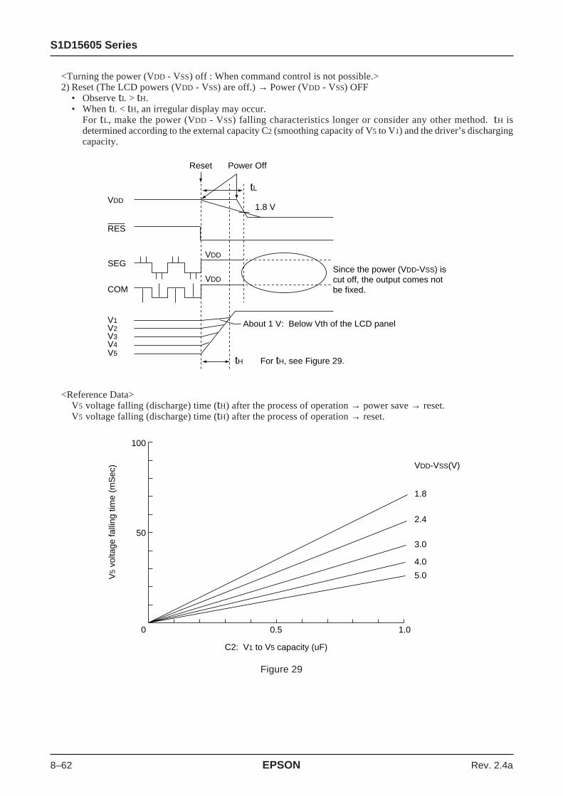
S1D15605 Series
8–62 EPSON Rev. 2.4a
<Turning the power (VDD - VSS) off : When command control is not possible.>2) Reset (The LCD powers (VDD - VSS) are off.) → Power (VDD - VSS) OFF
• Observe tL > tH.• When tL < tH, an irregular display may occur.
For tL, make the power (VDD - VSS) falling characteristics longer or consider any other method. tH isdetermined according to the external capacity C2 (smoothing capacity of V5 to V1) and the driver’s dischargingcapacity.
<Reference Data>V5 voltage falling (discharge) time (tH) after the process of operation → power save → reset.V5 voltage falling (discharge) time (tH) after the process of operation → reset.
Figure 29
tL
1.8 V
Since the power (VDD-VSS) is cut off, the output comes not be fixed.
About 1 V: Below Vth of the LCD panel
tH For tH, see Figure 29.
V1V2V3V4V5
COM
SEG
Power OffReset
VDD
VDD
VDD
RES
100
50
0 0.5
C2: V1 to V5 capacity (uF)
1.0
1.8
VDD-VSS(V)
V5
volta
ge fa
lling
tim
e (m
Sec
)
2.4
3.0
4.0
5.0

S1D15605 Series
Rev. 2.4a EPSON 8–63
• In case of other models than the above<Turning the power (VDD - VSS) off>
Power save (The LCD powers (VDD - VSS) are off.) -> Power (VDD - VSS) OFF• Observe tL > tH.• When tL < tH, an irregular display may occur.
Set tL on the MPU according to the software. tH is determined according to the external capacity C (smoothingcapacity of V5 to V1) and the external resisters Ra + Rb (for V5 voltage regulation)
tL
1.8 V
Since the power (VDD-VSS) is cut off, the output comes not be fixed.
About 1 V: Below Vth of the LCD panel
tH tH is determined depending on the timeconstant of (Ra + Rb) C.
V1V2V3V4V5
COM
SEG
Powersave
PowerOff
VDD

S1D15605 Series
8–64 EPSON Rev. 2.4a
VDD VDD
VSS2, V1 to V4
V5, VOUT
VCC
GND VSS
S1D15605 Series chip sideSystem (MPU) side
9. ABSOLUTE MAXIMUM RATINGSUnless otherwise noted, VSS = 0 V
Parameter Symbol Conditions UnitPower Supply Voltage VDD –0.3 to +7.0 V
Power supply voltage (2) VSS2 –7.0 to +0.3 V(VDD standard) With Triple step-up –6.0 to +0.3
With Quad step-up –4.5 to +0.3Power supply voltage (3) (VDD standard) V5, VOUT –18.0 to +0.3 V
Power supply voltage (4) (VDD standard) V1, V2, V3, V4 V5 to +0.3 VInput voltage VIN –0.3 to VDD + 0.3 V
Output voltage VO –0.3 to VDD + 0.3 V
Operating temperature TOPR –40 to +85 °CStorage temperature TCP TSTR –55 to +100
Bare chip –55 to +125 °C
Figure 30
Notes and Cautions1. The VSS2, V1 to V5 and VOUT are relative to the VDD = 0V reference.2. Insure that the voltage levels of V1, V2, V3, and V4 are always such that VDD ≥ V1 ≥ V2 ≥ V3 ≥ V4 ≥ V5.3. Permanent damage to the LSI may result if the LSI is used outside of the absolute maximum ratings. Moreover,
it is recommended that in normal operation the chip be used at the electrical characteristic conditions, and use ofthe LSI outside of these conditions may not only result in malfunctions of the LSI, but may have a negativeimpact on the LSI reliability as well.
Table 17

S1D15605 Series
Rev. 2.4a EPSON 8–65
10. DC CHARACTERISTICSUnless otherwise specified, VSS = 0 V, VDD = 3.0 V ± 10%, Ta = –40 to 85°C
Item Symbol ConditionRating
UnitsApplicable
Min. Typ. Max. PinOperating Recom- VDD 2.7 — 3.3 V VDD*1
Voltage (1) mendedVoltagePossible 1.8 — 5.5 V VDD*1
OperatingVoltage
Operating Recom- VSS2 (Relative to VDD) –3.3 — –2.7 V VSS2
Voltage (2) mendedVoltagePossible VSS2 (Relative to VDD) –6.0 — –1.8 V VSS2
OperatingVoltage
Operating Possible V5 (Relative to VDD) –16.0 — –4.5 V V5 *2Voltage (3) Operating
VoltagePossible V1, V2 (Relative to VDD) 0.4 × V5 — VDD V V1, V2
OperatingVoltagePossible V3, V4 (Relative to VDD) V5 — 0.6 × V5 V V3, V4
OperatingVoltage
High-level Input VIHC 0.8 × VDD — VDD V *3VoltageLow-level Input VILC VSS — 0.2 × VDD V *3Voltage
High-level Output VOHC IOH = –0.5 mA 0.8 × VDD — VDD V *4VoltageLow-level Output VOLC IOL = 0.5 mA VSS — 0.2 × VDD V *4Voltage
Input leakage ILI VIN = VDD or VSS –1.0 — 1.0 µA *5currentOutput leakage ILO –3.0 — 3.0 µA *6current
Liquid Crystal Driver RON Ta = 25°C V5 = –14.0 V — 2.0 3.5 kΩ SEGnON Resistance (Relative To VDD) V5 = –8.0 V — 3.2 5.4 kΩ COMn *7
Static Consumption ISSQ — 0.01 5 µA VSS, VSS2
CurrentOutput Leakage I5Q V5 = –18.0 V — 0.01 15 µA V5
Current (Relative To VDD)
Input Terminal CIN Ta = 25°C f = 1 MHz — 5.0 8.0 pFCapacitance
Oscillator Internal fOSC Ta = 25°C 18 22 26 kHz *8Frequency Oscillator
External fCL S1D15605*****/15607***** 18 22 26 kHz CLInput
Internal fOSC Ta = 25°C 27 33 39 kHz *8OscillatorExternal fCL S1D15606*****/15608*****/ 14 17 20 kHz CLInput 15609*****
Table 18

S1D15605 Series
8–66 EPSON Rev. 2.4a
Item Symbol ConditionRating
UnitsApplicable
Min. Typ. Max. PinInput voltage VSS2 With Triple –6.0 — –1.8 V VSS2
(Relative To VDD)VSS2 With Quad –4.5 — –1.8 V VSS2
(Relative To VDD)
Supply Step-up VOUT (Relative to VDD) –18.0 — — V VOUToutput voltageCircuit
Voltage regulator VOUT (Relative to VDD) –18.0 — –6.0 V VOUTCircuit OperatingVoltageVoltage Follower V5 (Relative to VDD) –16.0 — –4.5 V V5 *9Circuit OperatingVoltage
Base Voltage VREG0 Ta = 25°C –0.05%/°C –2.04 –2.10 –2.16 V *10VREG1 (Relative to VDD) –0.2%/°C –4.65 –4.9 –5.15 V *10
Inte
rnal
Pow
er
Table 19

S1D15605 Series
Rev. 2.4a EPSON 8–67
• Dynamic Consumption Current (1), During Display, with the Internal Power Supply OFFCurrent consumed by total ICs when an external power supply is used.
• Dynamic Consumption Current (2), During Display, with the Internal Power Supply ONThe values of curret consumed in all the IC including internal power supply circuit.
Ta = 25°C
Item Symbol ConditionRating
Units NotesMin. Typ. Max.
S1D15605***** IDD (1) VDD = 5.0 V, V5 – VDD = –11.0 V — 23 38 µA *11VDD = 3.0 V, V5 – VDD = –11.0 V — 21 35
S1D15606***** VDD = 3.0 V, V5 – VDD = –11.0 V — 17 29VDD = 5.0 V, V5 – VDD = –8.0 V — 14 24VDD = 3.0 V, V5 – VDD = –8.0 V — 12 20
S1D15607***** VDD = 5.0 V, V5 – VDD = –8.0 V — 11 18VDD = 3.0 V, V5 – VDD = –8.0 V — 10 17
S1D15608*****/ VDD = 5.0 V, V5 – VDD = –8.0 V — 15 25S1D15609***** VDD = 3.0 V, V5 – VDD = –8.0 V — 13 22
Table 21 Display Pattern Checker
Ta = 25°C
Item Symbol ConditionRating
Units NotesMin. Typ. Max.
S1D15605***** IDD (1) VDD = 5.0 V, V5 – VDD = –11.0 V — 18 30 µA *11VDD = 3.0 V, V5 – VDD = –11.0 V — 16 27
S1D15606***** VDD = 3.0 V, V5 – VDD = –11.0 V — 13 22VDD = 5.0 V, V5 – VDD = –8.0 V — 11 19VDD = 3.0 V, V5 – VDD = –8.0 V — 9 15
S1D15607***** VDD = 5.0 V, V5 – VDD = –8.0 V — 8 13VDD = 3.0 V, V5 – VDD = –8.0 V — 7 12
S1D15608*****/ VDD = 5.0 V, V5 – VDD = –8.0 V — 12 20S1D15609***** VDD = 3.0 V, V5 – VDD = –8.0 V — 10 17
Table 20 Display Pattern OFF
Ta = 25°C
Item Symbol ConditionRating
Units NotesMin. Typ. Max.
S1D15605***** IDD (2) VDD = 5.0 V, Triple step-up voltage. Normal Mode — 67 112 µA *12V5 – VDD = –11.0 V High-Power Mode — 114 190VDD = 3.0 V, Quad step-up voltage. Normal Mode — 81 135V5 – VDD = –11.0 V High-Power Mode — 138 230
S1D15606***** VDD = 5.0 V, Double step-up voltage. Normal Mode — 35 59V5 – VDD = –8.0 V High-Power Mode — 64 107VDD = 3.0 V, Triple step-up voltage. Normal Mode — 43 72V5 – VDD = –8.0 V High-Power Mode — 84 140VDD = 3.0 V, Quad step-up voltage. Normal Mode — 72 121V5 – VDD = –11.0 V High-Power Mode — 128 214
S1D15607***** VDD = 5.0 V, Double step-up voltage. Normal Mode — 26 44V5 – VDD = –8.0 V High-Power Mode — 60 100VDD = 3.0 V, Triple step-up voltage. Normal Mode — 29 49V5 – VDD = –8.0 V High-Power Mode — 73 122
S1D15608*****/ VDD = 5.0 V, Double step-up voltage. Normal Mode — 37 62S1D15609***** V5 – VDD = –8.0 V High-Power Mode — 67 112
VDD = 3.0 V, Triple step-up voltage. Normal Mode — 46 77V5 – VDD = –8.0 V High-Power Mode — 87 145
Table 22 Display Pattern OFF

S1D15605 Series
8–68 EPSON Rev. 2.4a
• Consumption Current at Time of Power Saver Mode, VSS = 0 V, VDD = 3.0 V ± 10%
Ta = 25°C
Item Symbol ConditionRating
Units NotesMin. Typ. Max.
S1D15605***** IDD (2) VDD = 5.0 V, Triple step-up voltage. Normal Mode — 81 135 µA *12V5 – VDD = –11.0 V High-Power Mode — 127 212VDD = 3.0 V, Quad step-up voltage. Normal Mode — 96 160V5 – VDD = –11.0 V High-Power Mode — 153 255
S1D15606***** VDD = 5.0 V, Double step-up voltage. Normal Mode — 41 69V5 – VDD = –8.0 V High-Power Mode — 71 119VDD = 3.0 V, Triple step-up voltage. Normal Mode — 51 85V5 – VDD = –8.0 V High-Power Mode — 92 154VDD = 3.0 V, Quad step-up voltage. Normal Mode — 85 142V5 – VDD = –11.0 V High-Power Mode — 142 237
S1D15607***** VDD = 5.0 V, Double step-up voltage. Normal Mode — 32 53V5 – VDD = –8.0 V High-Power Mode — 62 103VDD = 3.0 V, Triple step-up voltage. Normal Mode — 44 73V5 – VDD = –8.0 V High-Power Mode — 89 148
S1D15608*****/ VDD = 5.0 V, Double step-up voltage. Normal Mode — 44 74S1D15609***** V5 – VDD = –8.0 V High-Power Mode — 74 127
VDD = 3.0 V, Triple step-up voltage. Normal Mode — 54 90V5 – VDD = –8.0 V High-Power Mode — 95 159
Table 23 Display Pattern Checker
Ta = 25°C
Item Symbol ConditionRating
Units NotesMin. Typ. Max.
Sleep mode S1D15605***** IDDS1 — 0.01 5 µA
Standby Mode S1D15605***** IDDS2 — 4 8 µASleep mode S1D15606***** IDDS1 — 0.01 5 µA
Standby Mode S1D15606***** IDDS2 — 4 8 µASleep mode S1D15607***** IDDS1 — 0.01 5 µA
Standby Mode S1D15607***** IDDS2 — 3 6 µASleep mode S1D15608*****/ IDDS1 — 0.01 5 µA
S1D15609*****Standby Mode S1D15608*****/ IDDS2 — 4 8 µA
S1D15609*****
Table 24
TBD: To Be Determined

S1D15605 Series
Rev. 2.4a EPSON 8–69
Reference Data 1
• Dynamic Consumption Current (1) During LCD Display Using an External Power Supply
Figure 31
Figure 32
40
30
20
10
00 2 4 6 8
VDD [V]
IDD (
1) (
ISS +
I5)
[µA
]
Conditions: Internal power supply OFFExternal power supply in useS1D15605/S1D15606 (–11.0V):V5 – VDD = –11.0 VS1D15606 (–8.0V)/S1D15607/S1D15608/S1D15609:V5 – VDD = –8.0 VDisplay pattern: OFFTa = 25°C
Note: *11
S1D15605
S1D15606 (–11.0V)
S1D15606 (–8.0V)
S1D15607
S1D15608/S1D15609 (–8.0V)
40
30
20
10
00 2 4 6 8
VDD [V]
IDD (
1) (
ISS +
I5)
[µA
]
Internal power supply OFFExternal power supply in useS1D15605/S1D15606 (–11.0V):V5 – VDD = –11.0 VS1D15606 (–8.0V)/S1D15607/S1D15608/S1D15609:V5 – VDD = –8.0 VDisplay pattern: CheckerTa = 25°C
Note: *11
Conditions:
S1D15605
S1D15606 (–8.0V)S1D15608/S1D15609 (–8.0V)S1D15606 (–11.0V)
S1D15607

S1D15605 Series
8–70 EPSON Rev. 2.4a
Reference Data 2
• Dynamic Consumption Current (2) During LCD display using the internal power supply
Figure 33
Figure 34
Conditions: Internal power supply ONS1D15605/S1D15606 (×4, –11.0V)/S1D15608/S1D15609 (×4, –11.0V):4× step-up voltage: V5 – VDD = –11.0 VS1D15606 (×3, –8.0V)/S1D15607/S1D15608/S1D15609 (×3, –8.0V):3× step-up voltage: V5 – VDD = –8.0 VNormal modeDisplay pattern: OFFTa = 25°C
Note: *12
140
120
100
80
60
40
20
00 2 4 6 8
VDD [V]
IDD (
2) [µ
A] S1D15605
S1D15606 (x4, –11.0V)S1D15608/15609 (x4, –11.0V)
S1D15606 (x3, –8.0V)
S1D15607
S1D15608/S1D15609 (x3, –8.0V)
Internal power supply ONS1D15605/S1D15606 (×4, –11.0V)/S1D15608/S1D15609 (×4, –11.0V):4× step-up voltage: V5 – VDD = –11.0 VS1D15606 (×3, –8.0V)/S1D15607/S1D15608/S1D15609 (×3, –8.0V):3× step-up voltage: V5 – VDD = –8.0 VNormal modeDisplay pattern: CheckerTa = 25°C
Note: *12
Conditions:
120
100
80
60
40
20
00 2 4 6 8
VDD [V]
IDD (
2) [µ
A]
S1D15605
S1D15606 (x4, –11.0V)S1D15608/15609 (x4, –11.0V)
S1D15606 (x3, –8.0V)S1D15608/S1D15609 (x3, –8.0V)
S1D15607

S1D15605 Series
Rev. 2.4a EPSON 8–71
Reference Data 3
• Dynamic Consumption Current (3) During access
Figure 35
Reference Data 4
• Operating voltage range of VSS and V5 systems
Figure 36
S1D15605 Series Note: *2–20
–16
–7.2
–4.5
1.8 3.0 5.5
0 2
VDD[V]
4 6 8
–15
–10
V5-
VD
D[V
]
–5
0
Operating range
10
1
0.1
IDD(3
)[m
A]
0.010.001 0.01 0.1
fCYC[MHz]
1 10
This figure indicates the consumption current while the checker pattern is constantly written through fCYC. If there is no access, then only (1) remains.
Conditions: Internal power supply OFF,external power supply usedS1D15605:VDD – VSS = 3.0 V, V5=–11.0 VS1D15606/S1D15607/S1D15608/S1D15609:VDD – VSS = 3.0 V, V5=–8.0 VTa = 25°C
S1D15605S1D15606S1D15607S1D15608/S1D15609

S1D15605 Series
8–72 EPSON Rev. 2.4a
• The Relationship Between Oscillator Frequency fOSC, Display Clock Frequency fCL and the Liquid Crystal FrameRate Frequency fFR
References for items market with **1 While a broad range of operating voltages is guaranteed, performance cannot be guaranteed if there are
sudden fluctuations to the voltage while the MPU is being accessed.*2 The operating voltage range for the VDD system and the V5 system is as shown in Figure 36. This applies
when the external power supply is being used.*3 The A0, D0 to D5, D6 (SCL), D7 (SI), RD (E), WR (R/W), CS1, CS2, CLS, CL, FR, M/S, C86, P/S, DOF,
RES, IRS, and HPM terminals.*4 The D0 to D7, FR, FRS, DOF, and CL terminals.*5 The A0, RD (E), WR (R/W), CS1, CS2, CLS, M/S, C86, P/S, RES, IRS, and HPM terminals.*6 Applies when the D0 to D5, D6 (SCL), D7 (SI), CL, FR, and DOF terminals are in a high impedance state.*7 These are the resistance values for when a 0.1 V voltage is applied between the output terminal SEGn or
COMn and the various power supply terminals (V1, V2, V3, and V4). These are specified for the operatingvoltage (3) range.RON = 0.1 V/∆ I (Where ∆ I is the current that flows when 0.1 V is applied while the power supply is ON.)
*8 See Table 9-7 for the relationship between the oscillator frequency and the frame rate frequency.*9 The V5 voltage regulator circuit regulates within the operating voltage range of the voltage follower.*10 This is the internal voltage reference supply for the V5 voltage regulator circuit. In the S1D15605/S1D15606/
S1D15607 chips, the temperature range can come in three types as VREG options: (1) approximately–0.05%/°C,(2) –0.2%/°C, and (3) external input.
*11, 12 It indicates the current consumed on ICs alone when the internal oscillator circuit and display are turnedon.The S1D15605 is 1/9 biased, S1D15606/S1D15608/S1D15609 is 1/8 biased and S1D15607 is 1/6 biased.Does not include the current due to the LCD panel capacity and wiring capacity.Applicable only when there is no access from the MPU.
*12 It is the value on a model having the VREG option temperature gradient is –0.05%/°C when the V5 voltageregulator internal resistor is used.
Table 25
Item f CL fFR
S1D15605***** When the internal oscillator circuit is used fOSC fOSC____ _____4 4 × 65
When the internal oscillator circuit is not used External input (fCL) fCL____260
S1D15606***** When the internal oscillator circuit is used fOSC fOSC____ _____8 8 × 49
When the internal oscillator circuit is not used External input (fCL) fCL____196
S1D15607***** When the internal oscillator circuit is used fOSC fOSC____ _____8 8 × 33
When the internal oscillator circuit is not used External input (fCL) fCL____264
S1D15608***** When the internal oscillator circuit is used fOSC fOSC____ _____8 8 × 55
When the internal oscillator circuit is not used External input (fCL) fCL____220
S1D15609***** When the internal oscillator circuit is used fOSC fOSC____ _____8 8 × 53
When the internal oscillator circuit is not used External input (fCL) fCL____212
(fFR is the liquid crystal alternating current period, and not the FR signal period.)

S1D15605 Series
Rev. 2.4a EPSON 8–73
11. TIMING CHARACTERISTICS(1) System Bus Read/Write Characteristics 1 (For the 8080 Series MPU)
Figure 37
(VDD = 4.5 V to 5.5 V, Ta = –40 to 85°C )
Item Signal Symbol ConditionRating
UnitsMin. Max.
Address hold time A0 tAH8 0 — nsAddress setup time tAW8 0 — ns
System cycle time A0 tCYC8 166 — nsControl LOW pulse width (WR) WR tCCLW 30 — nsControl LOW pulse width (RD) RD tCCLR 70 — nsControl HIGH pulse width (WR) WR tCCHW 30 — nsControl HIGH pulse width (RD) RD tCCHR 30 — ns
Data setup time D0 to D7 tDS8 30 — nsAddress hold time tDH8 10 — nsRD access time tACC8 CL = 100 pF — 70 nsOutput disable time tOH8 5 50 ns
Table 26
A0
*1
*2
CS1(CS2="1")
WR, RD
D0 to D7(Write)
D0 to D7(Read)
tACC8 tOH8
tf tr
tDS8
tCYC8
tAH8tAW8
tCCLR, tCCLW
tCCHR, tCCHW
tDH8
CS1(CS2="1")
WR, RD
S1D15605 Series
8–74 EPSON Rev. 2.4a
(VDD = 2.7 V to 4.5 V, Ta = –40 to 85°C )
Item Signal Symbol ConditionRating
UnitsMin. Max.
Address hold time A0 tAH8 0 — nsAddress setup time tAW8 0 — ns
System cycle time A0 tCYC8 300 — nsControl LOW pulse width (WR) WR tCCLW 60 — nsControl LOW pulse width (RD) RD tCCLR 120 — nsControl HIGH pulse width (WR) WR tCCHW 60 — nsControl HIGH pulse width (RD) RD tCCHR 60 — ns
Data setup time D0 to D7 tDS8 40 — nsAddress hold time tDH8 15 — nsRD access time tACC8 CL = 100 pF — 140 nsOutput disable time tOH8 10 100 ns
Table 27
(VDD = 1.8 V to 2.7 V, Ta = –40 to 85°C )
Item Signal Symbol ConditionRating
UnitsMin. Max.
Address hold time A0 tAH8 0 — nsAddress setup time tAW8 0 — nsSystem cycle time A0 tCYC8 1000 — ns
Control LOW pulse width (WR) WR tCCLW 120 — nsControl LOW pulse width (RD) RD tCCLR 240 — nsControl HIGH pulse width (WR) WR tCCHW 120 — nsControl HIGH pulse width (RD) RD tCCHR 120 — nsData setup time D0 to D7 tDS8 80 — nsAddress hold time tDH8 30 — ns
RD access time tACC8 CL = 100 pF — 280 nsOutput disable time tOH8 10 200 ns
Table 28
*1 This is in the case of making the access by WR and RD,setting the CS1=LOW.*2 This is the case of making the accese by CS1,setting the WR,RD=LOW.*3 The rise and fall times (tr and tf) of the input signal are specified for less than 15 ns.When using the
system cycle time at high speed, they are specified for (tr + tf) ≤ (tCYC8-tCCLR-tCCHR).*4 All timings are specified based on the 20 and 80% of VDD.*5 tCCLW and tCCLR are specified for the overlap period when CS1 is at LOW (CS2=HIGH) level and
WR,RD are at the LOW level.
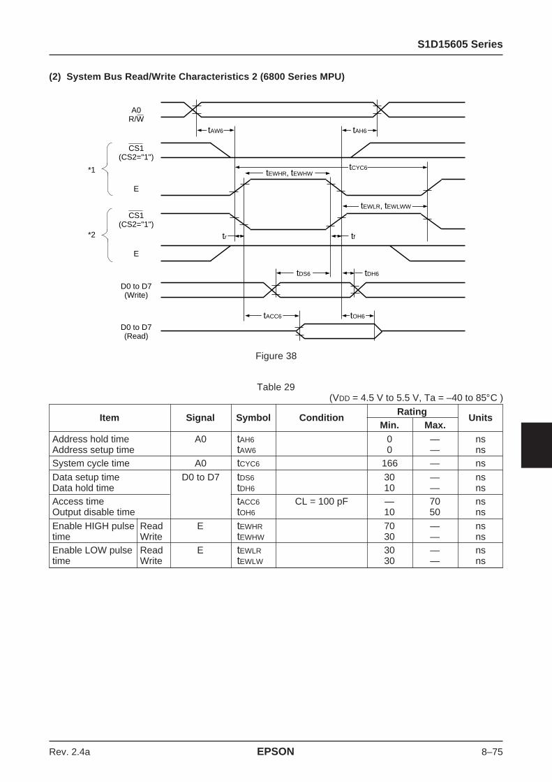
S1D15605 Series
Rev. 2.4a EPSON 8–75
(VDD = 4.5 V to 5.5 V, Ta = –40 to 85°C )
Item Signal Symbol ConditionRating
UnitsMin. Max.
Address hold time A0 tAH6 0 — nsAddress setup time tAW6 0 — nsSystem cycle time A0 tCYC6 166 — ns
Data setup time D0 to D7 tDS6 30 — nsData hold time tDH6 10 — nsAccess time tACC6 CL = 100 pF — 70 nsOutput disable time tOH6 10 50 ns
Enable HIGH pulse Read E tEWHR 70 — nstime Write tEWHW 30 — nsEnable LOW pulse Read E tEWLR 30 — nstime Write tEWLW 30 — ns
Table 29
(2) System Bus Read/Write Characteristics 2 (6800 Series MPU)
Figure 38
A0R/W
*1
*2
CS1(CS2="1")
E
D0 to D7(Write)
D0 to D7(Read)
tACC6 tOH6
tDS6
tCYC6
tAH6tAW6
tEWHR, tEWHW
tEWLR, tEWLWW
tDH6
tftr
CS1(CS2="1")
E

S1D15605 Series
8–76 EPSON Rev. 2.4a
(VDD = 2.7 V to 4.5 V, Ta = –40 to 85°C )
Item Signal Symbol ConditionRating
UnitsMin. Max.
Address hold time A0 tAH6 0 — nsAddress setup time tAW6 0 — ns
System cycle time A0 tCYC6 300 — nsData setup time D0 to D7 tDS6 40 — nsData hold time tDH6 15 — ns
Access time tACC6 CL = 100 pF — 140 nsOutput disable time tOH6 10 100 nsEnable HIGH pulse Read E tEWHR 120 — nstime Write tEWHW 60 — ns
Enable LOW pulse Read E tEWLR 60 — nstime Write tEWLW 60 — ns
Table 30
(VDD = 1.8 V to 2.7 V, Ta = –40 to 85°C )
Item Signal Symbol ConditionRating
UnitsMin. Max.
Address hold time A0 tAH6 0 — nsAddress setup time tAW6 0 — ns
System cycle time A0 tCYC6 1000 — nsData setup time D0 to D7 tDS6 80 — nsData hold time tDH6 30 — ns
Access time tACC6 CL = 100 pF — 280 nsOutput disable time tOH6 10 200 nsEnable HIGH pulse Read E tEWHR 240 — nstime Write tEWHW 120 — ns
Enable LOW pulse Read E tEWLR 120 — nstime Write tEWLW 120 — ns
Table 31
*1 This is in the case of making the access by E, setting the CS1=LOW.*2 This is the case of making the accese by CS1,setting the E=HIGH.*3 The rise and fall times ((tr and tf) of the input signal are specified for less than 15 ns.When using the
system cycle time at high speed, they are specified for (tr + tf) ≤ (tCYC6-tEWLW-tEWHW) or (tr + tf) ≤(tCYC6-tEWLR-tEWHR).
*4 All timings are specified based on the 20 and 80% of VDD.*5 tEWLW and tEWLR are specified for the overlap period when CS1 is at LOW (CS2=HIGH) level and E
is at the HIGH level.

S1D15605 Series
Rev. 2.4a EPSON 8–77
(VDD = 4.5 V to 5.5 V, Ta = –40 to 85°C )
Item Signal Symbol ConditionRating
UnitsMin. Max.
Serial Clock Period SCL tSCYC 200 — nsSCL HIGH pulse width tSHW 75 — nsSCL LOW pulse width tSLW 75 — nsAddress setup time A0 tSAS 50 — nsAddress hold time tSAH 100 — ns
Data setup time SI tSDS 50 — nsData hold time tSDH 50 — nsCS-SCL time CS tCSS 100 — ns
tCSH 100 — ns
Table 32
(3) The Serial Interface
Figure 39
tCSS tCSH
tSAH
tSHW
tSDHtSDS
tSLW
tftr
tSCYC
tSAS
CS1(CS2="1")
A0
SCL
SI

S1D15605 Series
8–78 EPSON Rev. 2.4a
(VDD = 2.7 V to 4.5 V, Ta = –40 to 85°C )
Item Signal Symbol ConditionRating
UnitsMin. Max.
Serial Clock Period SCL tSCYC 250 — nsSCL HIGH pulse width tSHW 100 — nsSCL LOW pulse width tSLW 100 — ns
Address setup time A0 tSAS 150 — nsAddress hold time tSAH 150 — nsData setup time SI tSDS 100 — nsData hold time tSDH 100 — ns
CS-SCL time CS tCSS 150 — nstCSH 150 — ns
Table 33
(VDD = 1.8 V to 2.7 V, Ta = –40 to 85°C )
Item Signal Symbol ConditionRating
UnitsMin. Max.
Serial Clock Period SCL tSCYC 400 — nsSCL HIGH pulse width tSHW 150 — nsSCL LOW pulse width tSLW 150 — ns
Address setup time A0 tSAS 250 — nsAddress hold time tSAH 250 — nsData setup time SI tSDS 150 — nsData hold time tSDH 150 — ns
CS-SCL time CS tCSS 250 — nstCSH 250 — ns
Table 34
*1 The input signal rise and fall time (tr, tf) are specified at 15 ns or less.*2 All timing is specified using 20% and 80% of VDD as the standard.

S1D15605 Series
Rev. 2.4a EPSON 8–79
(4) Display Control Output Timing
Figure 40
(VDD = 4.5 V to 5.5 V, Ta = –40 to 85°C)
Item Signal Symbol ConditionRating
UnitsMin. Typ. Max.
FR delay time FR tDFR CL = 50 pF — 10 40 ns
Table 35
(VDD = 2.7 V to 4.5 V, Ta = –40 to 85°C)
Item Signal Symbol ConditionRating
UnitsMin. Typ. Max.
FR delay time FR tDFR CL = 50 pF — 20 80 ns
Table 36
(VDD = 1.8 V to 2.7 V, Ta = –40 to 85°C)
Item Signal Symbol ConditionRating
UnitsMin. Typ. Max.
FR delay time FR tDFR CL = 50 pF — 50 200 ns
Table 37
*1 Valid only when the master mode is selected.*2 All timing is based on 20% and 80% of VDD.
tDFR
CL(OUT)
FR

S1D15605 Series
8–80 EPSON Rev. 2.4a
(VDD = 4.5 V to 5.5 V, Ta = –40 to 85°C)
Item Signal Symbol ConditionRating
UnitsMin. Typ. Max.
Reset time tR — — 0.5 µs
Reset LOW pulse width RES tRW 0.5 — — µs
Table 38
(VDD = 2.7 V to 4.5 V, Ta = –40 to 85°C)
Item Signal Symbol ConditionRating
UnitsMin. Typ. Max.
Reset time tR — — 1 µsReset LOW pulse width RES tRW 1 — — µs
Table 39
(VDD = 1.8 V to 2.7 V, Ta = –40 to 85°C)
Item Signal Symbol ConditionRating
UnitsMin. Typ. Max.
Reset time tR — — 1.5 µsReset LOW pulse width RES tRW 1.5 — — µs
*1 All timing is specified with 20% and 80% of VDD as the standard.
Table 40
Reset Timing
Figure 41
tRW
tR
Reset completeDuring reset
RES
Internalstatus

S1D15605 Series
Rev. 2.4a EPSON 8–81
12. THE MPU INTERFACE (REFERENCE EXAMPLES)The S1D15605 Series can be connected to either 80 × 86 Series MPUs or to 6800 Series MPUs. Moreover, using theserial interface it is possible to operate the S1D15605 series chips with fewer signal lines.The display area can be enlarged by using multiple S1D15605 Series chips. When this is done, the chip select signalcan be used to select the individual ICs to access.
(1) 8080 Series MPUs
Figure 42-1
(2) 6800 Series MPUs
Figure 42-2
(3) Using the Serial Interface
Figure 42-3
VDDVCC
GND
Decoder
RESET
MP
U
A0
D0 to D7RDWRRES
CS1CS2
A0
D0 to D7RDWR
RES
A1 to A7IORQ
VDD
C86
P/SVSS
VSS
S1D
1560
5 S
erie
s
VDDVCC
GND
Decoder
RESET
MP
U
A0
D0 to D7ER/WRES
CS1CS2
A0
D0 to D7E
R/WRES
A1 to A15VMA
VDD
C86
P/SVSS
VSS
S1D
1560
5 S
erie
s
VDDVCC
GND
Decoder
RESET
MP
U
A0
SISCLRES
CS1CS2
A0
Port 1Port 2
RES
A1 to A7
VDD or VSS
C86
P/SVSS
VSS
S1D
1560
5 S
erie
s

S1D15605 Series
8–82 EPSON Rev. 2.4a
13. CONNECTIONS BETWEEN LCD DRIVERS (REFERENCE EXAMPLE)The liquid crystal display area can be enlarged with ease through the use of multiple S1D15605 Series chips. Use a sameequipment type.
(1) S1D15605 (master) ↔ S1D15605 (slave)
Figure 43
VSS
VDD
M/S
Output InputS1D
1560
5 S
erie
sM
aste
rM/S
FR
CL
DOF
FR
CL
DOF
S1D
1560
5 S
erie
sS
lave

S1D15605 Series
Rev. 2.4a EPSON 8–83
14. CONNECTIONS BETWEEN LCD DRIVERS (REFERENCE EXAMPLES)The liquid crystal display area can be enlarged with ease through the use of multiple S1D15605 Series chips.Use a same equipment type, in the composition of these chips.
(1) Single-chip Structure
Figure 44-1
(2) Double-chip Structure, #1
Figure 44-2
132 x 65 Dots
COM SEG COM
S1D15605 SeriesMaster
264 x 65 Dots
COM COMSEG SEG
S1D15605 SeriesMaster
S1D15605 SeriesSlave

S1D15605 Series
8–84 EPSON Rev. 2.4a
FR
CL
DOF
CS1
CS2
RES
A0
WR,R/W
RD, E
D0
D1
D2
D3
D4
D5
D6, SCL
D7, SI
VDD
VSS
VSS2
VOUT
CAP3-
CAP1+
CAP1-
CAP2-
CAP2+
VRS
VDD
V1
V2
V3
V4
V5
VR
VDD
M/S
CLS
C86
P/S
HPM
IRS
FR
FRS
COM S
COM 63
COM 33
COM 32
SEG 131
SEG 130
SEG 1
SEG 0
COM S
COM 0
COM 30
COM 31
•
•
•
•
•
•
•
•
•
•
•
•
•
•
•
CH
IP T
OP
VIE
W
An example
15. A SAMPLE TCP PIN ASSIGNMENTS1D15605T00B* TCP Pin LayoutNote: The following does not specify dimensions of the TCP pins.

S1D15605 Series
Rev. 2.4a EPSON 8–85
16. EXTERNAL VIEW OF TCP PINS
Spe
cific
atio
ns •
Bas
e: U
-rex
S, 7
5µm
• C
oppe
r fo
il: E
lect
roly
tic c
oppe
r fo
il, 2
5µm
• S
n pl
atin
g •
Pro
duct
pitc
h: 4
1P (
19.0
mm
) •
Sol
der
resi
st p
ositi
onal
tole
ranc
e: ±
0.3
(Mol
d, m
arki
ng a
rea)
(Mold, marking area)(Mold, marking area)
(Mol
d, m
arki
ng a
rea)
Sec
tion
A
Sec
tion
A
Sec
tion
A O
utpu
t ter
min
al p
atte
rn s
hape
Sec
tion
B T
est p
at d
etai
led
view

International Sales Operations AMERICA EPSON ELECTRONICS AMERICA, INC. HEADQUARTERS 150 River Oaks Parkway San Jose, CA 95134, U.S.A. Phone: +1-800-228-3964 FAX: +1-408-922-0238 SALES OFFICES West 1960 E.Grand Avenue Flr 2 El Segundo, CA 90245, U.S.A. Phone: +1-800-249-7730 FAX: +1-310-955-5400 Central 101 Virginia Street, Suite 290 Crystal Lake, IL 60014, U.S.A. Phone: +1-800-853-3588 FAX: +1-815-455-7633 Northeast 301 Edgewater Place, Suite 210 Wakefield, MA 01880, U.S.A. Phone: +1-800-922-7667 FAX: +1-781-246-5443 Southeast 3010 Royal Blvd. South, Suite 170 Alpharetta, GA 30005, U.S.A. Phone: +1-877-332-0020 FAX: +1-770-777-2637 EUROPE EPSON EUROPE ELECTRONICS GmbH HEADQUARTERS Riesstrasse 15 80992 Munich, GERMANY Phone: +49-89-14005-0 FAX: +49-89-14005-110 DÜSSELDORF BRANCH OFFICE Altstadtstrasse 176 51379 Leverkusen, GERMANY Phone: +49-2171-5045-0 FAX: +49-2171-5045-10 FRENCH BRANCH OFFICE 1 Avenue de l’ Atlantique, LP 915 Les Conquerants Z.A. de Courtaboeuf 2, F-91976 Les Ulis Cedex, FRANCE Phone: +33-1-64862350 FAX: +33-1-64862355 BARCELONA BRANCH OFFICE Barcelona Design Center Edificio Testa, C/Alcalde Barnils 64-68, Modulo C 2a planta E-08190 Sant Cugat del Vallès, SPAIN Phone: +34-93-544-2490 FAX: +34-93-544-2491
UK & IRELAND BRANCH OFFICE 8 The Square, Stockley Park, Uxbridge Middx UB11 1FW, UNITED KINGDOM Phone: +44-1295-750-216/+44-1342-824451 FAX: +44-89-14005 446/447 Scotland Design Center Integration House, The Alba Campus Livingston West Lothian, EH54 7EG, SCOTLAND Phone: +44-1506-605040 FAX: +44-1506-605041
ASIA EPSON (CHINA) CO., LTD. 23F, Beijing Silver Tower 2# North RD DongSanHuan ChaoYang District, Beijing, CHINA Phone: +86-10-6410-6655 FAX: +86-10-6410-7320 SHANGHAI BRANCH 7F, High-Tech Bldg., 900, Yishan Road, Shanghai 200233, CHINA Phone: +86-21-5423-5522 FAX: +86-21-5423-5512 EPSON HONG KONG LTD. 20/F., Harbour Centre, 25 Harbour Road Wanchai, Hong Kong Phone: +852-2585-4600 FAX: +852-2827-4346 Telex: 65542 EPSCO HX EPSON TAIWAN TECHNOLOGY & TRADING LTD. 14F, No. 7, Song Ren Road, Taipei 110 Phone: +886-2-8786-6688 FAX: +886-2-8786-6677 HSINCHU OFFICE No. 99, Jiangong Road, Hsinchu City 300 Phone: +886-3-573-9900 FAX: +886-3-573-9169 EPSON SINGAPORE PTE., LTD. 401 Commonwealth Drive, #07-01 Haw Par Technocentre, SINGAPORE 149598 Phone: +65-6586-3100 FAX: +65-6472-4291 SEIKO EPSON CORPORATION KOREA OFFICE 50F, KLI 63 Bldg., 60 Yoido-dong Youngdeungpo-Ku, Seoul, 150-763, KOREA Phone: +82-2-784-6027 FAX: +82-2-767-3677 GUMI OFFICE 2F, Grand B/D, 457-4 Songjeong-dong, Gumi-City, KOREA Phone: +82-54-454-6027 FAX: +82-54-454-6093 SEIKO EPSON CORPORATION SEMICONDUCTOR OPERATIONS DIVISION IC Sales Dept. IC Marketing Group 421-8, Hino, Hino-shi, Tokyo 191-8501, JAPAN Phone: +81-42-587-5814 FAX: +81-42-587-5117
Document Code: 410282901 First Issue May 2001
Printed August 2005 in JAPAN


![Introduction fo FPV Series Multilayer Chip Varistor - … · Introduction fo FPV Series Multilayer Chip Varistor Multilayer Chip ... 8063[3225] and 1080 ... l Provides On-Board Transient](https://static.fdocuments.us/doc/165x107/5b42af3a7f8b9ad23b8b5239/introduction-fo-fpv-series-multilayer-chip-varistor-introduction-fo-fpv-series.jpg)

