Chip Resistor Array Series - ElecFans
13
厚 聲 電 子 工 業 有 限 公 司 UNIROYAL ELECTRONICS INDUSTRY CO., LTD. Approved Checked Prepared File NO. Edition Date Page William Zhao Ted Hsu Chengxia Tang CS-01-065 1 2017/06/23 2/14 Contents Introduction ………………………………………………………………………………………Page 1.0 Scope ………………………………………………………………………………………….4 2.0 Type Designation……………………………………………………………………………..4 3.0 Ratings & Dimension ………………………………………………………………………..4~6 4.0 Structure………………………………………………………………………………………..6 5.0 Marking ………………………………………… … ………………………………………7~8 6.0 Power rating…………………………...……………… ………………………………………9 7.0 Performance Specification ………………………………………………………………….. 9~10 8.0 Explanation of Part No. System ……………………………………………………………..11 9.0 Ordering Procedure …………………………………………………………………………...12 10.0 Standard Packing …………………………………………………………………………12~13 11.0 Precaution for storage/Transportation………………………..……………......................14
Transcript of Chip Resistor Array Series - ElecFans
厚 聲 電 子 工 業 有 限 公 司 UNIROYAL ELECTRONICS INDUSTRY CO., LTD.
Approved Checked Prepared File NO. Edition Date Page
William Zhao Ted Hsu Chengxia Tang CS-01-065 1 2017/06/23 2/14
Contents
Introduction ………………………………………………………………………………………Page
1.0 Scope ………………………………………………………………………………………….4
2.0 Type Designation……………………………………………………………………………..4
3.0 Ratings & Dimension ………………………………………………………………………..4~6
4.0 Structure………………………………………………………………………………………..6
5.0 Marking ………………………………………… … ………………………………………7~8
6.0 Power rating…………………………...……………… ………………………………………9
7.0 Performance Specification ………………………………………………………………….. 9~10
8.0 Explanation of Part No. System ……………………………………………………………..11
9.0 Ordering Procedure …………………………………………………………………………...12
10.0 Standard Packing …………………………………………………………………………12~13
11.0 Precaution for storage/Transportation………………………..……………......................14
厚 聲 電 子 工 業 有 限 公 司 UNIROYAL ELECTRONICS INDUSTRY CO., LTD.
Approved Checked Prepared File NO. Edition Date Page
William Zhao Ted Hsu Chengxia Tang CS-01-065 1 2017/06/23 3/14
File Name:
Resistor Array Series
±1%、±5% & 0Ω
Date 2017/06/23 Edition No. 1
Amendment Record Signature
Edition Prescription of
amendment Amend Page Amend Date Amended by Checked by

厚 聲 電 子 工 業 有 限 公 司 UNIROYAL ELECTRONICS INDUSTRY CO., LTD.
Approved Checked Prepared File NO. Edition Date Page
William Zhao Ted Hsu Chengxia Tang CS-01-065 1 2017/06/23 4/14
1.0 Scope:
This sheet is the statement of the Chip Resistor Array- Concave Terminal specification that
UNIOHM’S productions can meet.
2.0 Type Designation:
The type designation shall be in the following from:
Example:
Type Power rating Resistance tolerance Nominal resistance
4C02 1/16W J 100
3.0 Ratings & Dimension:
3.1 Equivalent Circuit Diagram:
2D02/2D03
/2C02/2F01
4D02/4D03
/4C02/4C03/4F01 16P8
R1=R2 R1=R2=R3=R4
R1=R2=R3=R4=R5=R6=R7=R8
3.2 Dimensions in mm:
Convex Terminal type
2D02/2D03 4D02/4D03 16P8

厚 聲 電 子 工 業 有 限 公 司 UNIROYAL ELECTRONICS INDUSTRY CO., LTD.
Approved Checked Prepared File NO. Edition Date Page
William Zhao Ted Hsu Chengxia Tang CS-01-065 1 2017/06/23 5/14
Concave Terminal
2C02 4C02/4C03
Flat Terminal
2F01 4F01
Dimensions (mm) Type
L W T A1 A2 B P G
2D02 1.00±0.10 1.00±0.10 0.35±0.10 0.33±0.10 / 0.15±0.05 0.65±0.05 0.25±0.10
4D02 2.00±0.10 1.00±0.10 0.45±0.10 0.40±0.05 0.30±0.05 0.20±0.15 0.50±0.05 0.30±0.15
2D03 1.60±0.15 1.60±0.15 0.50±0.10 0.60±0.15 / 0.30±0.10 0.80±0.05 0.25±0.10
4D03 3.20±0.20 1.60±0.20 0.50±0.10 0.65±0.15 0.50±0.15 0.30±0.15 0.80±0.10 0.30±0.15
16P8 4.00±0.20 1.60±0.15 0.45±0.10 0.45±0.05 0.30±0.05 0.30±0.15 0.50±0.05 0.40±0.15
2C02 1.00±0.10 1.00±0.10 0.35±0.10 / / 0.15±0. 10 / 0.30±0.10
4C02 2.00±0.10 1.00±0.10 0.45±0.10 / / 0.15±0.10 / 0.30±0.10
4C03 3.20±0.20 1.60±0.20 0.60±0.10 / / 0.30±0.20 / 0.40±0.10
2F01 0.80±0.10 0.60±0.10 0.35±0.10 0.30±0.10 / 0.15±0.10 0.50±0.05 0.15±0.10
4F01 1.40±0.10 0.60±0.10 0.35±0.10 0.20±0.10 / 0.15±0.10 0.40±0.05 0.15±0.10

厚 聲 電 子 工 業 有 限 公 司 UNIROYAL ELECTRONICS INDUSTRY CO., LTD.
Approved Checked Prepared File NO. Edition Date Page
William Zhao Ted Hsu Chengxia Tang CS-01-065 1 2017/06/23 6/14
3.3 Ratings:
Type
Rated
power
70
Max
Working
Voltage
Max
Overload
Voltage
Dielectric
Withstanding
Voltage
Resistance
Range
±5%±1%
Temperature
Coefficient
PPM/
Operating
Temperature
Resistance
Value of
Jumper
Rated
Current
of Jumper
2D02 1/16W 50V 100V 100V 10Ω~1MΩ ±200
4D02 1/16W 50V 100V 100V 10Ω~1MΩ ±200
2D03 1/16W 50V 100V 100V 10Ω~1MΩ ±200
4D03 1/16W 50V 100V 300V 1Ω~1MΩ≥10Ω:±200
<10Ω:±400
4DP3 1/10W 50V 100V 300V 1Ω~1MΩ≥10Ω:±200
<10Ω:±400
16P8 1/16W 50V 100V 300V 1Ω~1MΩ≥10Ω:±200
<10Ω:±400
2C02 1/16W 50V 100V 100V 10Ω~1MΩ ±200
4C02 1/16W 50V 100V 100V 10Ω~1MΩ ±200
4C03 1/16W 50V 100V 300V 1Ω~1MΩ≥10Ω:±200
<10Ω:±400
-55~+155 <50mΩ 1A
2F01 1/20W 12.5V 25V / 10Ω~1MΩ ±200
4F01 1/20W 12.5V 25V / 10Ω~1MΩ ±200 -55~+125 <50mΩ 1A
4.0 Structure:
1: High purity alumina substrate
2: Protective covering
3: Resistive covering
4: Termination(inner)Ag/Pd
5: Termination(between)Ni plating
6: Termination(outer)Sn plating
厚 聲 電 子 工 業 有 限 公 司 UNIROYAL ELECTRONICS INDUSTRY CO., LTD.
Approved Checked Prepared File NO. Edition Date Page
William Zhao Ted Hsu Chengxia Tang CS-01-065 1 2017/06/23 7/14
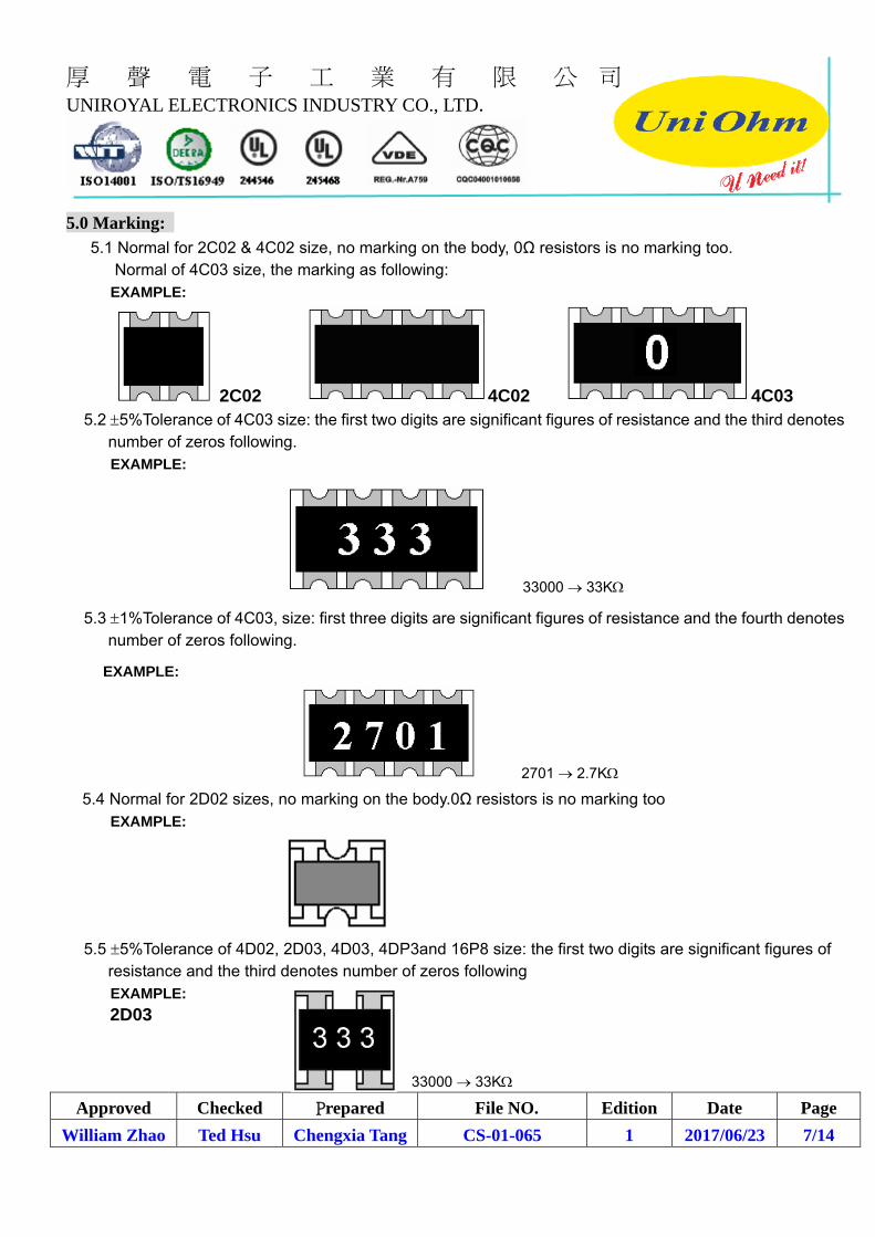
5.0 Marking: 5.1 Normal for 2C02 & 4C02 size, no marking on the body, 0Ω resistors is no marking too.
Normal of 4C03 size, the marking as following: EXAMPLE:
2C02 4C02 4C03 5.2 5%Tolerance of 4C03 size: the first two digits are significant figures of resistance and the third denotes
number of zeros following. EXAMPLE:
33000 33K
5.3 1%Tolerance of 4C03, size: first three digits are significant figures of resistance and the fourth denotes number of zeros following.
EXAMPLE:
2701 2.7K
5.4 Normal for 2D02 sizes, no marking on the body.0Ω resistors is no marking too EXAMPLE:
5.5 5%Tolerance of 4D02, 2D03, 4D03, 4DP3and 16P8 size: the first two digits are significant figures of resistance and the third denotes number of zeros following EXAMPLE:
2D03
33000 33K
厚 聲 電 子 工 業 有 限 公 司 UNIROYAL ELECTRONICS INDUSTRY CO., LTD.
Approved Checked Prepared File NO. Edition Date Page
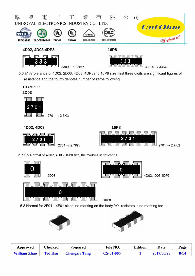
William Zhao Ted Hsu Chengxia Tang CS-01-065 1 2017/06/23 8/14
4D02, 4D03,4DP3 16P8
33000 33K 33000 33K
5.6 1%Tolerance of 4D02, 2D03, 4D03, 4DP3and 16P8 size: first three digits are significant figures of
resistance and the fourth denotes number of zeros following
EXAMPLE:
2D03
2701 2.7K
4D02, 4D03 16P8
2701 2.7K 2701 2.7K
5.7 0ΩNormal of 4D02, 4D03, 16P8 size, the marking as following:
2D03 4D02,4D03,4DP3
16P8
5.8 Normal for 2F01,4F01 sizes, no marking on the body.0Ω resistors is no marking too

厚 聲 電 子 工 業 有 限 公 司 UNIROYAL ELECTRONICS INDUSTRY CO., LTD.
Approved Checked Prepared File NO. Edition Date Page
William Zhao Ted Hsu Chengxia Tang CS-01-065 1 2017/06/23 9/14
6.0 Power Rating: Resistors shall have a power rating based on continuous load operation at an ambient temperature from -55 to 70. For temperature in excess of 70, the load shall be derate as shown in figure 1
6.1 Voltage rating: Resistors shall have a rated direct-current (DC) continuous working Voltage or an approximate sine-wave root-mean-square (RMS) alternating-current (AC) continuous working voltage at commercial-line frequency and waveform corresponding to the power rating, as determined from the following formula:
RCWV = R P Where: RCWV commercial-line frequency and waveform (Volt.)
P = power rating (VATT.) R = nominal resistance (OHM)
The overload voltage is 2.5 times RCWV or Max. Overload voltage whichever is less. In no case shall the rated DC or RMS AC continuous working voltage be greater than the applicable maximum value.
7.0 Performance Specification:
Characteristic Limits Test Method (JIS-C-5201&5202)
Temperature Coefficient Reference 3.3
4.8 natural resistance changes per temp. Degree centigrade R2-R1 × 106 (PPM/) R1(T2-T1) R1: resistance value at room temp. (T1) R2: resistance value at room temp. +100 (Tt2) Test pattern: room temp. (T1), room temp. +100(T2)
±(2%+0.1Ω) MAX 2F01: 1%:±1%+0.05Ω
5%:±2%+0.05Ω
4.13 Permanent resistance change after the application of 2.5 times RCWV for 5 seconds. *Short-time
overload * ∆R<50mΩ Apply max overload current for 0Ω
* Insulation resistance ≥1,000 MΩ
4.6 the measuring voltage shall be ,measured with a direct voltage of (100±15)v or a voltage equal to the dielectric withstanding voltage., and apply for 1min

厚 聲 電 子 工 業 有 限 公 司 UNIROYAL ELECTRONICS INDUSTRY CO., LTD.
Approved Checked Prepared File NO. Edition Date Page
William Zhao Ted Hsu Chengxia Tang CS-01-065 1 2017/06/23 10/14
Terminal bending ±(1%+0.05Ω) Max 4.33 Twist of test board:
Y/x = 3/90 mm for 60Seconds
* Dielectric withstanding
voltage
No evidence of flashover mechanical damage, arcing or insulation breaks down.
4.7 Resistors shall be clamped in the trough of a 90metallic v-block and shall be tested at ac potential respectively specified in the given list of each product type for 60-70 seconds.
Soldering heat
Resistance change rate is: ±(1%+0.05Ω) Max
4.18 Dip the resistor into a solder bath having a temperature of 2605 and hold it for 10±1 seconds.
95% coverage Min. Wave solder: Test temperature of solder: 245±3 dipping time in solder: 2-3 seconds.
*Solderability Go up tin rate bigger than half of end pole
Reflow:
Temperature
cycling
ΔR/R≤±(1.0%+0.05Ω)
2F01: 1%:±0.5%+0.05Ω
5%:±1%+0.05Ω
4.19Resistance change after continuous five cycles for duty cycle specified below:
STEP TEMPERATURE TIME
1 -55±3 30 MINS 2 ROOM TEMP. 10 --- 15 MINS3 +155±2 30 MINS
4 ROOM TEMP. 10 --- 15 MINS*Step1-4 Continuous 5 cycles
±(3.0%±0.1Ω)Max. 2F01: 1%:±2%+0.1Ω
5%:±3%±0.1Ω
7.9 Resistance change after 1,000 hours (1.5 hours “ON”,0.5 hour “OFF”) at RCWV in a humidity chamber controlled at 40±2 and 90 to 95% relative humidity.
*Load life in humidity
* ∆R<50mΩ Apply to rated current for 0Ω
±(3.0%±0.1Ω)Max. 2F01: 1%:±2%+0.1Ω
5%:±3%±0.1Ω
4.25.1 Permanent resistance change after 1,000 hours operating at RCWV with duty cycle 1.5 hours “ON”,0.5 hour “OFF”, at 70±2 ambient. *Load life
* ∆R<50mΩ Apply to rated current for 0Ω
The resistors of 0Ω only can do the characteristic noted of *

厚 聲 電 子 工 業 有 限 公 司 UNIROYAL ELECTRONICS INDUSTRY CO., LTD.
Approved Checked Prepared File NO. Edition Date Page
William Zhao Ted Hsu Chengxia Tang CS-01-065 1 2017/06/23 11/14
8.0 Explanation of Part No. System: The standard Part No. includes 14 digits with the following explanation:
8.1 This is to indicate the Chip Array Resistor size.
Example: 2D02,4D02,2D03,4D03,4DP3,16P8,2C02, 4C02, 4C03,2F01,4F01
8.2 5th~6th digits:
8.2.1 This is to indicate the wattage or power rating. To dieting the size and the numbers,
The following codes are used; and please refer to the following chart for detail:
W=Normal Size; “1"~“G"to denotes“1"~“16"as Hexadecimal:
1/16W~1W:
Wattage 1/2 1/8 1/10 1/16
Normal Size W2 W8 WA WG
8.2.2 For power rating less than 1 watt, the 5th digit will be the letters W to represent the size
required & the 6th digit will be a number or a letter code.
Example: WG=1/16W
8.3 The 7th digit is to denote the Resistance Tolerance. The following letter code is to be used for
indicating the standard Resistance Tolerance.
F=±1% G=±2% J=±5% K= ±10%
8.4 The 8th to 11th digits is to denote the Resistance Value.
8.4.1 For the standard resistance values of E-24 series, the 8th digit is “0",the 9th & 10th digits are
to denote the significant figures of the resistance and the 11th digit is the number of zeros
following;
For the standard resistance values of E-96 series, the 8th digit to the 10th digits is to denote the
significant figures of the resistance and the 11th digit is the zeros following.
8.4.2 The following number s and the letter codes are to be used to indicate the number of zeros in the
11th digit:
0=100 1=101 2=102 3=103 4=104 5=105 6=106 J=10-1 K=10-2 L=10-3 M=10-4
8.4.3 The 12th, 13th & 14th digits.
The 12th digit is to denote the Packaging Type with the following codes:
C=Bulk in (Chip Product) T=Tape/Reel
8.4.4 The 13th digit is normally to indicate the Packing Quantity of Tape/Box & Tape/Reel packaging
types. The following letter code is to be used for some packing quantities:
1=1000pcs 2=2000pcs 3=3000pcs 4=4000pcs
5=5000pcs C=10000pcs D=20000pcs E=15000pcs
8.4.5 For some items, the 14th digit alone can use to denote special features of additional information
with the following codes:
E=For “Environmental Protection, Lead Free type"of Chip.
厚 聲 電 子 工 業 有 限 公 司 UNIROYAL ELECTRONICS INDUSTRY CO., LTD.
Approved Checked Prepared File NO. Edition Date Page
William Zhao Ted Hsu Chengxia Tang CS-01-065 1 2017/06/23 12/14
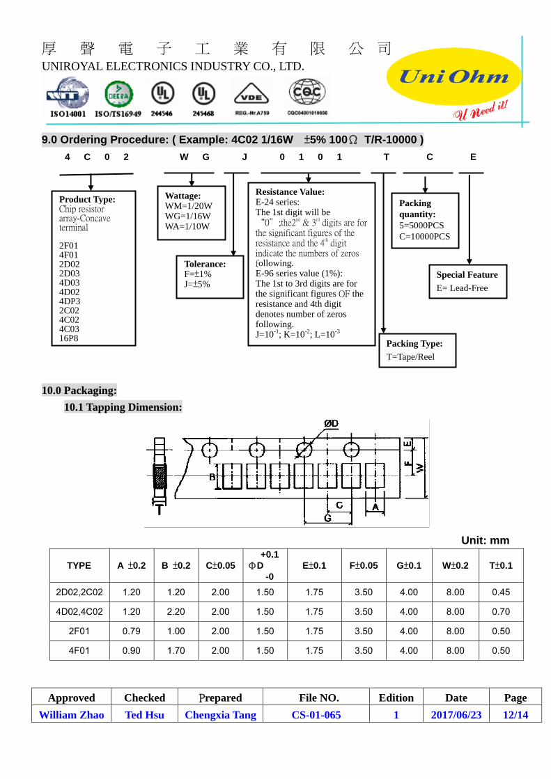
9.0 Ordering Procedure: ( Example: 4C02 1/16W ±5% 100Ω T/R-10000 )
4 C 0 2 W G J 0 1 0 1 T C E
10.0 Packaging:
10.1 Tapping Dimension:
Unit: mm
TYPE A ±0.2 B ±0.2 C±0.05 +0.1
ΦD -0
E±0.1 F±0.05 G±0.1 W±0.2 T±0.1
2D02,2C02 1.20 1.20 2.00 1.50 1.75 3.50 4.00 8.00 0.45
4D02,4C02 1.20 2.20 2.00 1.50 1.75 3.50 4.00 8.00 0.70
2F01 0.79 1.00 2.00 1.50 1.75 3.50 4.00 8.00 0.50
4F01 0.90 1.70 2.00 1.50 1.75 3.50 4.00 8.00 0.50
Product Type: Chip resistor array-Concave terminal 2F01 4F01 2D02 2D03 4D03 4D02 4DP3 2C02 4C02 4C03 16P8
Wattage: WM=1/20W WG=1/16W WA=1/10W
Tolerance: F=±1% J=±5%
Resistance Value:E-24 series: The 1st digit will be “0";the2nd & 3rd digits are for the significant figures of the resistance and the 4th digit indicate the numbers of zeros following. E-96 series value (1%): The 1st to 3rd digits are for the significant figures OF the resistance and 4th digit denotes number of zeros following. J=10-1; K=10-2; L=10-3
Packing Type:
T=Tape/Reel
Packing quantity: 5=5000PCS C=10000PCS
Special Feature
E= Lead-Free
厚 聲 電 子 工 業 有 限 公 司 UNIROYAL ELECTRONICS INDUSTRY CO., LTD.
Approved Checked Prepared File NO. Edition Date Page
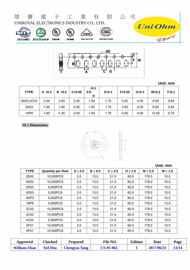
William Zhao Ted Hsu Chengxia Tang CS-01-065 1 2017/06/23 13/14
Unit: mm
TYPE A ±0.2 B ±0.2 C±0.05 +0.1
ΦD -0
E±0.1 F±0.05 G±0.1 W±0.2 T±0.1
4D03,4C03 2.00 3.60 2.00 1.50 1.75 3.50 4.00 8.00 0.83
2D03 1.90 1.90 2.00 1.50 1.75 3.50 4.00 8.00 0.83
16P8 1.80 4.30 2.00 1.50 1.75 5.50 4.00 12.00 0.75
10.2 Dimension:
Unit: mm TYPE Quantity per Reel A 0.5 B 0.5 C 0.5 D 1.0 M 2.0 W 1.0
2D02 10,000PCS 2.0 13.0 21.0 60.0 178.0 10.0
4D02 10,000PCS 2.0 13.0 21.0 60.0 178.0 10.0
2D03 5,000PCS 2.0 13.0 21.0 60.0 178.0 10.0
4D03 5,000PCS 2.0 13.0 21.0 60.0 178.0 10.0
4DP3 5,000PCS 2.0 13.0 21.0 60.0 178.0 10.0
16P8 4,000PCS 2.0 13.0 21.0 60.0 178.0 13.8
2C02 10,000PCS 2.0 13.0 21.0 60.0 178.0 10.0
4C02 10,000PCS 2.0 13.0 21.0 60.0 178.0 10.0
4C03 5,000PCS 2.0 13.0 21.0 60.0 178.0 10.0
2F01 10,000PCS 2.0 13.0 21.0 60.0 178.0 10.0
4F01 10,000PCS 2.0 13.0 21.0 60.0 178.0 10.0

厚 聲 電 子 工 業 有 限 公 司 UNIROYAL ELECTRONICS INDUSTRY CO., LTD.
Approved Checked Prepared File NO. Edition Date Page
William Zhao Ted Hsu Chengxia Tang CS-01-065 1 2017/06/23 14/14
11.0 Precaution for storage/Transportation:
11.1 UNIOHM recommend the storage condition temperature: 15~35, humidity :25%~75%.
(Put condition for individual product)
Even under UNIOHM recommended storage condition, solderability of products over 1 year old. (Put
condition for each product) may be degraded.
11.2 Store / transport cartons in the correct direction, which is indicated on a carton as a symbol.
Otherwise bent leads may occur due to excessive stress applied when dropping of a carton.
11.3 Product performance and soldered connections may deteriorate if the products are stored in the
following places:
a. Storage in high Electrostatic
b. Storage in direct sunshine、rain and snow or condensation
c. Where the products are exposed to sea winds or corrosive gases, including Cl2, H2S3 NH3, SO2,
NO2.