Report No: AN127 In-System Programming (ISP) of … · Application Note 127 - In-System Programming...
24
Application Note 127 - In-System Programming (ISP) of the Atmel XMEGA AVR FLASH Microcontroller Family 31 st March 2010 1 Report No: AN127 Title: In-System Programming (ISP) of the Atmel XMEGA AVR FLASH Microcontroller Family Author: Date: Version Number: John Marriott 7 th May 2010 0.98 preliminary All rights are reserved. Reproduction in whole or in part is prohibited without the prior written consent of the copyright owner. The information presented in this document does not form part of any quotation or contract, is believed to be accurate and reliable and may be changed without prior notice. No liability will be accepted by the publisher for any consequence of its use. Publication thereof does not convey nor imply any license under patent or other industrial or intellectual property rights
Transcript of Report No: AN127 In-System Programming (ISP) of … · Application Note 127 - In-System Programming...
Application Note 127 - In-System Programming (ISP) of the Atmel XMEGA AVR FLASH Microcontroller Family 31st March 2010
1
Report No:
AN127 Title:
In-System Programming (ISP) of the Atmel XMEGA AVR FLASH Microcontroller Family Author: Date: Version Number:
John Marriott
7th May 2010 0.98 preliminary
All rights are reserved. Reproduction in whole or in part is prohibited without the prior written consent of the copyright owner. The information presented in this document does not form part of any quotation or contract, is believed to be accurate and reliable and may be changed without prior notice. No liability will be accepted by the publisher for any consequence of its use. Publication thereof does not convey nor imply any license under patent or other industrial or intellectual property rights
Application Note 127 - In-System Programming (ISP) of the Atmel XMEGA AVR FLASH Microcontroller Family 31st March 2010
2
Contents 1.0 Introduction.................................................................................................................................... 3
1.1 Programmers supporting XMEGA PDI and JTAG ..................................................................... 3 1.2 XMEGA Device Support............................................................................................................. 4
2.0 XMEGA Programming Interfaces ................................................................................................. 5 2.1 Overview of XMEGA Programming Interfaces........................................................................... 5 2.2 Comparison of XMEGA PDI and JTAG algorithms.................................................................... 6 2.3 Overview of PDI Interface .......................................................................................................... 8 2.4 PDI – Physical Interface............................................................................................................. 8 2.5 Overview of JTAG Interface....................................................................................................... 9
3.0 PDI Algorithm............................................................................................................................... 11 3.1 Overview of PDI Interface ........................................................................................................ 11 3.2 PDI – Physical Interface........................................................................................................... 11 3.3 PDI – Clock Signal (XMEGA RESET pin) ................................................................................ 12 3.4 PDI – Data Signal .................................................................................................................... 12 3.5 ISPnano Series 3 - Target ISP Port – PDI pin-out ................................................................... 13 3.5 Single XMEGA device – PDI programming connections ......................................................... 14 3.6 Single XMEGA PDI + AVR SPI – programming connections .................................................. 16 3.7 Signal / Power GROUND (0V) connections ............................................................................. 18 3.8 Enabling PDI programming mode............................................................................................ 18
Appendix 1 – CONMOD Module + XMEGA PDI ............................................................................... 20 1.0 Overview .................................................................................................................................. 20
Appendix 2 – ISPnano-QC1 Quick Connect Module ...................................................................... 22 1.0 Overview .................................................................................................................................. 22 1.1 Quick-Connect connector pin-out............................................................................................. 23

Application Note 127 - In-System Programming (ISP) of the Atmel XMEGA AVR FLASH Microcontroller Family 31st March 2010
3
1.0 Introduction This application note describes how to develop and implement In-System Programming (ISP) support for the Atmel ATxmega AVR microcontroller family using both the ‘2-wire PDI’ and ‘4-wire JTAG’ programming interfaces. The document details how to create a ‘Programming Project’ which will operate on any Equinox ISP programmer. The document describes the physical connections required from the programmer to the target Microcontroller and also details the different ISP Header Connector pin-outs which are currently available. 1.1 Programmers supporting XMEGA PDI and JTAG Programming support for the Atmel xmega microcontroller family is currently only available on the ‘ISPnano Series 3’ range of programmers. We have developed the PDI algorithm first and we are now looking into developing the JTAG algorithm. The table below details the Equinox ISP programmers which are capable of supporting PDI / JTAG programming of Atmel XMEGA AVR microcontrollers. Programmer PDI algorithm JTAG algorithm
ISPnano Series 3 Yes – available now
TBD – due Q3 2010
ISPnano Series 3 ATE Yes – available now
TBD – due Q3 2010
Please note:
• The ISPnano Series 3 programmer range supports uploading of up to 64 independent Standalone Programming Projects.
• The XMEGA 2-wire PDI programming interface cannot be supported on the Equinox FS2003, FS2009, Epsilon5, PPM3-MK2 or PPM4-MK1 programmers as these programmers do not feature the correct hardware to allow PDI to be implemented.
• In the future we hope to release support for programming of XMEGA devices via the JTAG interface for the Equinox FS2009 and PPM4-MK1 programmers.

Application Note 127 - In-System Programming (ISP) of the Atmel XMEGA AVR FLASH Microcontroller Family 31st March 2010
4
1.2 XMEGA Device Support The Equinox ‘ISPnano Series 3’ programmer is capable of supporting ‘2-wire PDI’ programming of the entire Atmel XMEGA AVR microcontroller family. The table below lists all the devices in the XMEGA ‘A1’ family.
The table below lists all the devices in the XMEGA ‘D4’ family.

Application Note 127 - In-System Programming (ISP) of the Atmel XMEGA AVR FLASH Microcontroller Family 31st March 2010
5
2.0 XMEGA Programming Interfaces 2.1 Overview of XMEGA Programming Interfaces The Atmel XMEGA AVR microcontroller family feature either one or both of the following physical interfaces: Interface Name
Interface description Number of interface signals
XMEGA pins required for programming
PDI Program and Debug Interface 2-wire • PDI_CLK • PDI_DATA
JTAG JTAG Program / Debug Interface 4-wire + RESET • TDI, TMI, TCK, TDO • RESET
A graphical overview of the ‘PDI’ and ‘JTAG’ interfaces is shown in the diagram below.
It is possible to perform both programming and debugging using either of the two physical interfaces. The primary interface is the ‘PDI Physical Interface’. This is a 2-pin interface which uses the RESET pin for the clock input (PDI_CLK), and the dedicated test pin PDI_DATA for data input and output A JTAG interface is also available on most devices (but not all), and this can be used for programming and debugging through the 4-pin JTAG interface. The JTAG interface is IEEE std. 1149.1 compliant, and supports JTAG boundary scan. Any external programmer or on-chip debugger/emulator can be directly connected to either of these interfaces.

Application Note 127 - In-System Programming (ISP) of the Atmel XMEGA AVR FLASH Microcontroller Family 31st March 2010
6
2.2 Comparison of XMEGA PDI and JTAG algorithms The table below compares the JTAG and SPI programming algorithms for the Atmel XMEGA AVR family of microcontrollers. Parameter
PDI algorithm JTAG algorithm Comments
PDI / JTAG Port availability
PDI port available on all XMEGA devices
JTAG port only available on higher pin-count XMEGA devices.
Use PDI if you need a common interface to all XMEGA devices. See note 1.
Programming speed Marginally faster than JTAG
Marginally slower than PDI
Depends on PDI / JTAG clock frequencies See note 2.
Programming reliability Very good
Very good Possible problems with PDI data integrity See note 3.
In-System Debugging Yes – use Atmel JTAG-ICE debugger
Yes – use Atmel JTAG-ICE debugger
JTAG port normally used during development phase for both PDI and JTAG. See note 4.
Boundary Scan Testing Not possible Yes – requires external JTAG tester
Very useful for production testing. See note 5.
Multiple XMEGA AVR programming on same Target Board
Very difficult in PDI mode
Possible to daisy-chain multiple XMEGA AVR devices in a JTAG chain.
Only one device can be programmed at a time. See note 6.
Programming pins required
2 pins PDI_CLK, PDI_DATA
4 pins + RESET TDI, TDO, TCK, TMS
PDI uses RESET pin for the PDI_CLK. See note 7.
Programming pins can be used for user I/O?
No – PDI pins are dedicated for programming.
Not recommended Try not to put other components on pins.
RESET pin control required?
Yes Yes The RESET pin is essential for SPI and JTAG operation. See note 7.
RESET pin isolation during programming
The PDI_CLK pin is the XMEGA RESET pin. Customer RESET circuit must be isolated during PDI programming.
No Careful design of the target RESET circuit is required to allow production programming via the PDI interface. See note 7.
PDI / JTAG Port availability (note 1) The 2-wire PDI port is available on all XMEGA devices in the family. The 4-wire JTAG port is only available on higher pin-count XMEGA devices. If you would like to use the same programming interface for all XMEGA devices, then PDI would be the best choice.

Application Note 127 - In-System Programming (ISP) of the Atmel XMEGA AVR FLASH Microcontroller Family 31st March 2010
7
Programming speed (note 2) It is likely that the PDI algorithm will be marginally faster than the JTAG algorithm as the JTAG algorithm is effectively the PDI protocol sent via JTAG with lots of passing bytes. So even though PDI features bidirectional data transfer, it will still probably be faster than JTAG. Programming reliability (note 3) The PDI algorithm uses a synchronous clock on the RESET pin of the XMEGA device. If there is any capacitance on the RESET pin eg. a CR reset circuit, then this could affect the reliability of PDI programming. In-System Debugging (note 4) The Atmel JTAG-ICE MK2 debugger supports debugging of XMEGA AVR microcontrollers via both the PDI and JTAG interface. Boundary Scan Testing (note 5) All XMEGA AVR devices which feature a JTAG port are capable of being tested in-circuit using the so called JTAG’ Boundary Scan Testing’ technique. This technique is not supported by Atmel or Equinox. It should be available on request from any good Boundary Scan Tester company. Multiple XMEGA AVR programming on same Target Board (note 6) It is possible to program multiple XMEGA AVR devices on the same Target Board using a single JTAG programming interface by connecting the XMEGA devices in a so called ‘JTAG Chain’. This mode will be supported by Equinox in the future. It is not possible to connect the PDI ports of multiple XMEGA AVR devices together. Each device would require its own dedicated PDI programmer. Programming pins required (note 6) The PDI interface only uses two pins on XMEGA device. The PDI_CLK pin is actually the XMEGA RESET pin, so this pin would not be used for user I/O anyway. The PDI_DATA pin is a dedicated pin only used for PDI so there are no user I/O pins wasted by using the PDI interface. However, one possible disadvantage of the PDI interface is that the PDI_CLK pin which is in fact the RESET pin cannot have any RESET circuit on it as this would skew the clock signal and stop PDI working. The RESET circuit on a PDI Target Board must therefore be carefully designed to allow PDI programming during production programming but also to act as a normal reset circuit during normal operation.
Application Note 127 - In-System Programming (ISP) of the Atmel XMEGA AVR FLASH Microcontroller Family 31st March 2010
8
2.3 Overview of PDI Interface The Program and Debug Interface (PDI) is an Atmel proprietary interface for external programming and on-chip debugging of Atmel XMEGA AVR microcontrollers. The PDI interface supports high-speed programming of all on-chip Non-Volatile Memory (NVM) spaces including the Flash, EEPROM, Fuses, Lockbits plus the User Signature Row. 2.4 PDI – Physical Interface The Program and Debug Interface (PDI) is a 2-wire interface which allows the XMEGA device to be programmed using an external programmer. The pins required for programming via the PDI interface are detailed in the table below. PDI Signal Name
Signal description Direction from programmer
Pin name on XMEGA device
PDI_CLK
PDI Clock Signal Output RESET
PDI_DATA PDI Data Signal (bi-directional)
Bi-directional TEST
GROUND (0V) Target / Programmer Signal GROUND Passive GND Vcc Target / Programmer Vcc Supply Passive VCC The connections between an ‘External programmer’ and the PDI Interface of an XMEGA device are shown in the diagram below.

Application Note 127 - In-System Programming (ISP) of the Atmel XMEGA AVR FLASH Microcontroller Family 31st March 2010
9
2.5 Overview of JTAG Interface The JTAG algorithm provides a method of performing high-speed programming of Atmel XMEGA AVR microcontroller devices. The same JTAG port can also be used for on-chip debugging of code using the Atmel JTAG-ICE Debugger. Fig 2.5 – XMEGA AVR – JTAG Programming Interface connections
TCK
TDI
TDO
TMS
Vcc
Vss
RESET
PROG_RESET
PROG_TCK
PROG_TDI
PROG_TDO
PROG_TMS
AtmelATmega
Microcontroller
PROG_VCC
PROG_GND
ResetCircuit
JTAG
PORT
Programmer Signal Name
Signal description Signal direction (from Programmer)
Connect to AVR Microcontroller Pin
Signal direction (from Microcontroller)
PROG_TCK Test Clock Pin Output TCK Input PROG_TDI Test Data Input Output TDI Input PROG_TDO Test Data Output Input TDO Output PROG_TMS Test Mode Select Output TMS Input PROG_RESET RESET Output RESET Input

Application Note 127 - In-System Programming (ISP) of the Atmel XMEGA AVR FLASH Microcontroller Family 31st March 2010
10
The advantages and disadvantages of the JTAG algorithm are detailed below. Advantages
• The JTAG algorithm uses the same ‘JTAG Port’ as the Atmel JTAG-ICE Debugger. This means that the same port can be used for both debugging during the development phase and also programming during the production phase of the product.
• It is possible to use the JTAG port of the Target Microcontroller to perform in-circuit testing of the microcontroller and surrounding circuitry. This testing is performed by shifting Test Data through the JTAG port of the Target Microcontroller. A JTAG Test System is required to perform this testing. It is not supported by any Equinox Programmer or the Atmel JTAG ICE.
• It is possible to daisy-chain multiple JTAG devices on the JTAG bus in a so-called ‘JTAG Chain’ and then select to program a particular device in the chain.
Disadvantages
• The JTAG algorithm is possibly marginally slower than the PDI algorithm. • The JTAG Programming Interface uses 5 pins: TCK, TDI, TDO, TMS and RESET. • The JTAG interface pins are all user I/O pins so the application will lose 4 I/O pins if JTAG is
used. • Not all XMEGA AVR devices have a JTAG port – only the larger pin-count devices can be
programmed via JTAG! • The JTAG pins of the microcontroller are not designed for off-board use and should not be
shared with any other circuitry on Target Board. This means that the JTAG port pins must be dedicated for programming / debugging.
Application Note 127 - In-System Programming (ISP) of the Atmel XMEGA AVR FLASH Microcontroller Family 31st March 2010
11
3.0 PDI Algorithm 3.1 Overview of PDI Interface The Program and Debug Interface (PDI) is an Atmel proprietary interface for external programming and on-chip debugging of Atmel XMEGA AVR microcontrollers. The PDI interface supports high-speed programming of all on-chip Non-Volatile Memory (NVM) spaces including the Flash, EEPROM, Fuses, Lockbits plus the User Signature Row. 3.2 PDI – Physical Interface The Program and Debug Interface (PDI) is a 2-wire interface which allows the XMEGA device to be programmed using an external programmer. The pins required for programming via the PDI interface are detailed in the table below. PDI Signal Name
Signal description Direction from programmer
Pin name on XMEGA device
PDI_CLK
PDI Clock Signal Output RESET
PDI_DATA PDI Data Signal (bi-directional)
Bi-directional TEST
GROUND (0V) Target / Programmer Signal GROUND Passive GND Vcc Target / Programmer Vcc Supply Passive VCC The connections between an ‘External programmer’ and the PDI Interface of an XMEGA device are shown in the diagram below.
Application Note 127 - In-System Programming (ISP) of the Atmel XMEGA AVR FLASH Microcontroller Family 31st March 2010
12
3.3 PDI – Clock Signal (XMEGA RESET pin) The ‘PDI – Clock’ is a clock signal which is continuously generated by the programmer during PDI programming. This clock is fed from the programmer into the PDI_CLK (RESET) pin of the target XMEGA device. The clock signal must be a continuous waveform with a frequency >= 10 kHz, otherwise the target XMEGA device will exit PDI programming mode. Important notes:
• As the XMEGA RESET pin is being used as a high-speed clock pin during PDI programming / debugging, it is therefore very important that this pin is free to oscillate without any external capacitive or resistive loading.
• The use of any form of reset circuit which prevents the external programmer from driving a clock into the RESET pin will probably cause the PDI programming to either be very unreliable or to not work at all.
• As the PDI_CLK (RESET) pin of the target XMEGA device is used as the PDI CLOCK pin, the RESET pin of the programmer must NOT be connected to this pin.
Recommendations:
• It is recommended that no other components are connected to the PDI_CLK (RESET) pin of the target XMEGA device during PDI programming.
• The programmer must connect directly to the actual PDI_CLK (RESET) pin of the XMEGA device.
• This can be achieved by using an ‘Option link’ or ‘0 ohm resistor’ on the PDI_CLK (RESET) pin which allows any other circuitry to be disconnected from this pin during PDI programming.
• If a capacitor must be placed on the PDI_CLK (RESET) pin for EMC purposes, then use the lowest value possible and isolate it from the actual PDI_CLK (RESET) pin by using e.g. a 10k ohm resistor.
3.4 PDI – Data Signal The PDI – Data is a bi-directional signal line which is used to transfer data between the programmer and the target XMEGA device and vice-versa. This is a dedicated pin for PDI programmer and should not be used for any other purposes except PDI. When PDI programming mode is first entered, the programmer automatically becomes the ‘master’ on the PDI bus and drives the PDI_DATA (TEST) signal line. As part of the PDI protocol, the programmer can then instruct the target XMEGA device to transmit data back to the programmer. In order to achieve this, the programmer must reverse the direction of the PDI_DATA signal so that the XMEGA device can then drive this line back to the programmer. The automatic reversal of the data direction is handled by special high-speed driver hardware on the external programmer. Recommendations:
• It is recommended that no other components are connected to the PDI_DATA (TEST) pin. • This pin must be dedicated for PDI data transfer.

Application Note 127 - In-System Programming (ISP) of the Atmel XMEGA AVR FLASH Microcontroller Family 31st March 2010
13
3.5 ISPnano Series 3 - Target ISP Port – PDI pin-out The ‘Target ISP Connector’ port of the ‘ISPnano Series 3’ programmer features all the signals required to implement In-System Programming (ISP) of a target XMEGA device using the ‘2-wire PDI’ interface. The illustration below shows the location of the ‘Target ISP Connector’ port on the rear panel of the programmer.
‘Target ISP Connector’ port The connector is a 16-pin bump-polarised IDC connector with 0.1” pin spacing. Pin 1 is the top right pin as shown in the diagram opposite.
This connector also features the programmable “Target Vcc” and “Target Vpp” voltages plus a switched “EXTERNAL Vcc” supply. The pins on this connector which are used for the ‘PDI Interface’ are detailed in the table below. Programmer Signal name (16-way IDC)
IDC pin
Signal description Direction from programmer
Pin name on XMEGA device
TARGET_VCC 1+2 Target Vcc Supply Passive VCC
GROUND (0V) 5+6 Target / Programmer Signal GROUND Passive GND
PDI_CLOCK 7 PDI Clock Signal Output RESET
PDI_DATA_TXD 8 PDI Data Signal - TRANSMIT Output TEST
PDI_SYNC 9 PDI Synchronisation Signal Output TEST
PDI_DATA_RXD 13 PDI Data Signal - RECEIVE Input TEST

Application Note 127 - In-System Programming (ISP) of the Atmel XMEGA AVR FLASH Microcontroller Family 31st March 2010
14
3.5 Single XMEGA device – PDI programming connections The diagram below shows the connections required between the programmer and a Target Board for programming a single XMEGA microcontroller using the PDI interface.
Vcc
AtmelXMEGA AVR
Microcontroller
> 10 kHz
PDI_DATA (TEST)
PDI_DATA_TXD (8)
PDI_DATA_RXD (13)(SPI - MISO / JTAG TDO)
PDI_CLK (RESET)PDI_CLOCK (7)
TARGET VCC (1+2)
GND
PROG_GND (5+6)
POWER GROUND(STAR connected EARTH point)
Target Board (UUT)
SIGNAL GROUND (0V)
PDI_SYNC (9)R1
ProgrammerTarget ISP Port
connector
TARGET VCC
PDIBI-DIRECTIONAL
DATA
Programmer Signal name (16-way IDC)
IDC pin
Signal description Direction from programmer
Pin name on XMEGA device
TARGET_VCC 1+2 Target Vcc Supply Passive VCC
GROUND (0V) 5+6 Target / Programmer Signal GROUND Passive GND
PDI_CLOCK 7 PDI Clock Signal Output RESET
PDI_DATA_TXD 8 PDI Data Signal - TRANSMIT Output TEST
PDI_SYNC 9 PDI Synchronisation Signal Output TEST
PDI_DATA_RXD 13 PDI Data Signal - RECEIVE Input TEST

Application Note 127 - In-System Programming (ISP) of the Atmel XMEGA AVR FLASH Microcontroller Family 31st March 2010
15
Please note: • The PDI_SYNC signal (pin 9 on the Target ISP connector) should be connected to the
XMEGA TEST (PDI_DATA) pin via a resistor – R1. The value of R1 should be 470 ohms. This pin is used to force the XMEGA device into PDI programming mode.
• The RESET line from the programmer must NOT be connected to the XMEGA device RESET pin (unless you are using some sort of external reset circuit).
• A separate "SIGNAL GROUND" and "POWER GROUND" should be implemented so that large fluctuations in the target 0V do not affect the PDI or SPI signals.
• The "SIGNAL GROUND" is connected between the programmer and the UUT 0V. • The "POWER GROUND" is connected between the UUT 0V and the ‘STAR Connected
EARTH’ of the fixture. This should be the common EARTH point for the power supplies which are powering the programmer(s) and the UUT(s).

Application Note 127 - In-System Programming (ISP) of the Atmel XMEGA AVR FLASH Microcontroller Family 31st March 2010
16
3.6 Single XMEGA PDI + AVR SPI – programming connections The diagram below shows the connections required between the programmer and the Target Board for programming both an XMEGA microcontroller and a standard AVR microcontroller on the same Target Board. This schematic shows how to program the following devices using a single programmer:
• Atmel XMEGA AVR microcontroller – PDI programming interface • Atmel standard AVR microcontroller – SPI programming interface
Vcc
AtmelXMEGA AVR
Microcontroller
> 10 kHz
PDI_DATA (TEST)
PDI_DATA_TXD (8)
PDI_DATA_RXD (13)(SPI - MISO / JTAG TDO)
PDI_CLK (RESET)PDI_CLOCK (7)
TARGET VCC (1+2)
GND
PROG_GND (5+6)
MISO
SCKPROG_SCK (12)
MOSI
GND
Vcc
RESET
PROG_MOSI (14)
PROG_RESET (16)
AtmelStandard AVR
Microcontroller(SPI Mode)
SIGNAL GROUND (0V)
PDIBI-DIRECTIONAL
DATA
SIGNAL GROUND (0V)
TARGET VCC
ProgrammerTarget ISP Port
connector
PDI_SYNC (9)R1
POWER GROUND(STAR connected EARTH point)
Target Board (UUT)

Application Note 127 - In-System Programming (ISP) of the Atmel XMEGA AVR FLASH Microcontroller Family 31st March 2010
17
Programmer Signal name (16-way IDC)
IDC pin
Signal description Direction from programmer
Pin name on target device
TARGET_VCC 1+2 Target Vcc Supply Passive VCC
GROUND (0V) 5+6 Target / Programmer Signal GROUND
Passive GND
PDI_CLOCK 7 PDI Clock Output XMEGA - RESET
PDI_DATA_TXD 8 PDI Data Signal - TRANSMIT Output XMEGA - TEST
PDI_SYNC 9 PDI Synchronisation Signal Output TEST
PROG_SCK 12 SPI – SCK Clock Output AVR - SCK
PDI_DATA_RXD PROG_MISO 13
PDI Data Signal – RECEIVE SPI – MISO
Input XMEGA- TEST
PROG_MOSI 14 SPI – MOSI signal Output AVR - MOSI
PROG_RESET 16 Programmer RESET – AVR SPI device
Output AVR - RESET
Please note:
• The PDI_SYNC signal (pin 9 on the Target ISP connector) should be connected to the XMEGA TEST (PDI_DATA) pin via a resistor – R1. The value of R1 should be 470 ohms. This pin is used to force the XMEGA device into PDI programming mode.
• It is also recommended that a resistor R2 (value 470 ohms) is inserted in the MISO line to protect the programmer against a clash of both the target device and programmer drive this signal by mistake at the same time.
• There is one shared programmer signal line between the "SPI" and "PDI" port. The MISO line is shared with the ‘PDI_DATA_RXD’ pin so this pin must be routed to both devices.
• When programming in PDI mode, it is important to keep the "AVR SPI" micro in reset (RESET pin held LOW) so that the AVR tri-states all its SPI lines allowing the MISO pin to be used as the ‘PDI_DATA_RXD’ pin. This can be done by setting the RESET pin to ‘LAL’ in the pre-programming state machine.
• The RESET line from the programmer must NOT be connected to the XMEGA device RESET pin (unless you are using some sort of external reset circuit).
• A separate "SIGNAL GROUND" and "POWER GROUND" should be implemented so that large fluctuations in the target 0V do not affect the PDI or SPI signals.
• The "SIGNAL GROUND" is connected between the programmer and the UUT 0V. • The "POWER GROUND" is connected between the UUT 0V and the ‘STAR Connected
EARTH’ of the fixture. This should be the common EARTH point for the power supplies which are powering the programmer(s) and the UUT(s).

Application Note 127 - In-System Programming (ISP) of the Atmel XMEGA AVR FLASH Microcontroller Family 31st March 2010
18
3.7 Signal / Power GROUND (0V) connections It is very important that both the programmer and Target System (UUT) are earthed correctly. Incorrect grounding can lead to current flowing in the 0V signal back to the PC which could cause ESD damage to either the programmer or the UUT. The ISPnano programmer features a ‘Signal GROUND’ which is a specially filtered (cleaned) 0V signal which is used only for the programming signals. The UUT should then use its own dedicated ‘Power GROUND’ as this will be much noisier the programmer 0V. Signal GROUND (0V) The ‘Signal GROUND’ is the 0V to which the programming signals (PDI, SPI, JTAG etc) are referenced to. This is a specially filtered 0V signal line which is used only for the programming signals. The ‘Signal GROUND’ should be connected from the GROUND pins on the ‘Target ISP Port’ connector directly to the main GROUND on the UUT. The minimum cable length should be used for this connection. Power GROUND (0V) The ‘Power GROUND’ is the 0V to which the Target Board (UUT) uses as its 0V reference. The ‘Power GROUND’ should be connected from the main GROUND (0V) point on the UUT to the ‘Star connected GROUND of the overall programming fixture. This is usually the point where all 0V GROUND connections are made for the power supplies in the fixture. 3.8 Enabling PDI programming mode The PDI port must be enabled before it can be used. The external programmer must first force the PDI_DATA (TEST) line high for a period longer than the equivalent external reset minimum pulse width (refer to device data sheet for external reset pulse width data). This will disable the RESET functionality of the RESET pin, if not already disabled by the fuse settings. This can be achieved by making the correct settings in the ‘Pre-programming statemachine’ in the EQTools programming project. The PDI_CLK (RESET) line must then be kept high for 16 PDI_CLK cycles (16 positive edges detected). The first PDI_CLK cycle must start no later than 100uS after the RESET functionality of the Reset pin was disabled. If this does not occur in time the RESET functionality of the Reset pin is automatically enabled again and the enabling procedure must start over again.

Application Note 127 - In-System Programming (ISP) of the Atmel XMEGA AVR FLASH Microcontroller Family 31st March 2010
19
Application Note 127 - In-System Programming (ISP) of the Atmel XMEGA AVR FLASH Microcontroller Family 31st March 2010
20
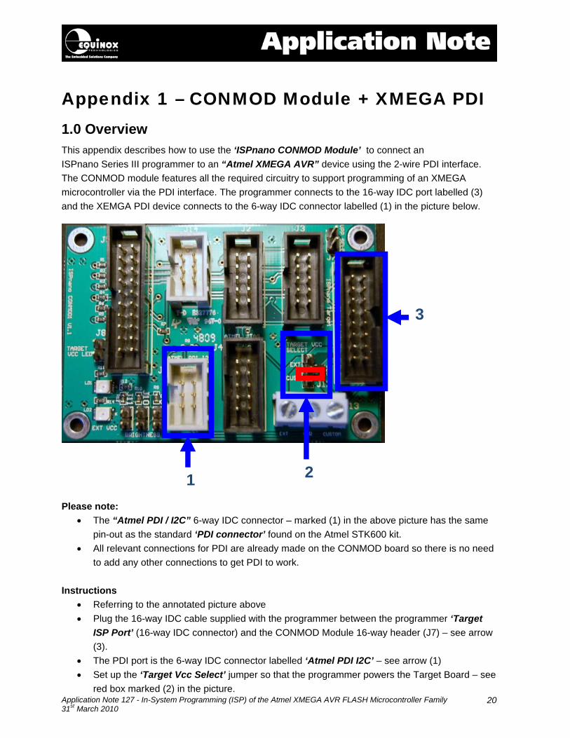
Appendix 1 – CONMOD Module + XMEGA PDI 1.0 Overview This appendix describes how to use the ‘ISPnano CONMOD Module’ to connect an ISPnano Series III programmer to an “Atmel XMEGA AVR” device using the 2-wire PDI interface. The CONMOD module features all the required circuitry to support programming of an XMEGA microcontroller via the PDI interface. The programmer connects to the 16-way IDC port labelled (3) and the XEMGA PDI device connects to the 6-way IDC connector labelled (1) in the picture below.
Please note:
• The “Atmel PDI / I2C” 6-way IDC connector – marked (1) in the above picture has the same pin-out as the standard ‘PDI connector’ found on the Atmel STK600 kit.
• All relevant connections for PDI are already made on the CONMOD board so there is no need to add any other connections to get PDI to work.
Instructions
• Referring to the annotated picture above • Plug the 16-way IDC cable supplied with the programmer between the programmer ‘Target
ISP Port’ (16-way IDC connector) and the CONMOD Module 16-way header (J7) – see arrow (3).
• The PDI port is the 6-way IDC connector labelled ‘Atmel PDI I2C’ – see arrow (1) • Set up the ‘Target Vcc Select’ jumper so that the programmer powers the Target Board – see
red box marked (2) in the picture.
1 2
3

Application Note 127 - In-System Programming (ISP) of the Atmel XMEGA AVR FLASH Microcontroller Family 31st March 2010
21

Application Note 127 - In-System Programming (ISP) of the Atmel XMEGA AVR FLASH Microcontroller Family 31st March 2010
22
Appendix 2 – ISPnano-QC1 Quick Connect Module 1.0 Overview This appendix describes the ‘ISPnano-QC1’ Quick Connect Module. This module features all the required circuitry required to implement XMEGA AVR programming via the 2-wire PDI programming interface. The module plugs into the 16-way ‘Target ISP Port’ on the ISPnano Series 3 programmer or Series 3 ATE programmer. It provides so-called ‘Quick connect’ connections allowing both an XMEGA PDI Target System and either a JTAG or SPI Target System to be connected to the programmer at the same time. Features
• Plugs into the 16-way ‘Target ISP Port’ on the ISPnano Series 3 programmer or Series 3 ATE programmer.
• Features all circuitry required for programming an Atmel XMEGA AVR microcontroller via the PDI interface
• Allows an second device to be connected to the same programmer via either the JTAG or SPI interface
• All Target I/O signals are available via Quick-connect connectors • External-Vcc in-line fuse • ‘Target Vcc’ LED • ‘External Vcc’ LED

Application Note 127 - In-System Programming (ISP) of the Atmel XMEGA AVR FLASH Microcontroller Family 31st March 2010
23
1.1 Quick-Connect connector pin-out The pin-out of the Quick Connect connectors is detailed in the table below. QC pin
QC Signal Name
Signal description Direction from programmer
Pin name on target device
1 VCC Target Vcc Supply Passive VCC
2 EXT EXTERNAL switched Target Vcc Supply Passive See note 1
3 GND Target / Programmer Signal GROUND Passive GND
4 CLK XMEGA PDI Clock Output XMEGA - RESET
5 DATA XMEGA PDI Data Output XMEGA - TEST
6 I/O5 Spare I/O
Input / Output
See note 2
7 I/O4 JTAG - TMS Output JTAG - TMS
8 I/O3 • SPI – SCK
• JTAG - TCK Output
• SPI – SCK • JTAG - TCK
9 I/O2 • SPI – MISO
• JTAG - TDO Input
• SPI – MISO • JTAG - TDO
10 I/O1 • SPI – MOSI
• JTAG - TDI Output
• SPI – MOSI • JTAG - TDI
11 RST RESET Output See note 3
12 VPP VPP Voltage PASSIVE See note 4
Please note:
• The signal names printed on the ’ISPnano-QC1’ Quick Connect Module are shown in the ‘QC Signal Name’ column in the table.
• The XMEGA ‘PDI Clock’ and ‘PDI Data’ signals are marked as ‘CLK’ and ‘DATA’ respectively and should be connected to the target XMEGA RESET pin and TEST pin
Note 1 The ‘EXTERNAL switched Target Vcc Supply’ is an external voltage applied to the ‘DC-EXT’ pin of the programmer which can be switched to the Target System. It is usually used to switch a voltage to the input of a voltage regulator circuit on the Target System. If you are not using this functionality, then do not connect this pin. Note 2 This is a spare I/O line which is not used for either the SPI or JTAG algorithms. Note 3 The RESET pin of the programmer should NOT be connected to the target XMEGA AVR RESET pin as XMEGAs use the RESET pin as the CLOCK pin.
Application Note 127 - In-System Programming (ISP) of the Atmel XMEGA AVR FLASH Microcontroller Family 31st March 2010
24
If you are planning to connect an SPI or JTAG device to the programmers as well as an XMEGA PDI device, then the RESET pin of the programmer should connect to the RESET pin of the SPI or JTAG device. Note 4 The VPP pin outputs a programmable voltage from 5.0 to 13.5V which is used to place certain devices eg. ATtiny microcontrollers into ‘High-voltage programming mode’. This pin should not be connected if you are programming any other devices.