CPLD ISP Programming Thro Micro Controller
23
XAPP058 (v4.1) March 6, 2009 www.xilinx.com 1 © 2001–2009 Xilinx, Inc. XILINX, the Xilinx logo, Virtex , Spartan, ISE, and other designated brands included herein are trademarks of Xilinx in the United States and other countries. All other trademarks are the property of their respective owners. Summary Xilinx® high-performance CPLD, FPGA, and configuration PROM families provide in-system programmability , reliable pi n locking, and IEEE Std 1149.1 (JT AG) boundary-scan test capability . This powerful combination of features allows designers to make significant changes and yet keep the original device pinouts, thus, eliminating the need to re-tool PC boards. By using an embedded processor to program these CPLDs and FPGAs from an onboard RAM or EPROM, designers can easily upgrade, modify , and test designs, even in the field. Xilinx Families This application note can be used with the following Xilinx device families: Vir tex® series, Spartan® series, CoolR unner® series, XC9500 seri es, Platform Flash PROM family , and XC18V00 family. Introduction The Xilinx CPLD and FPGA families combine superior performance with an advanced architecture to create new design opportunities that were previously impossible. The combination of in-system programmability , reliable pin locking, and JT AG test capability gives the following important benefits: • Reduces device handling costs and time to market • Saves the expense of laying out new PC boards • Allows remote maintenance, modification, and testing • Increases the life span and functionality of products • Enables unique, customer-specific features By using a simple JTA G interface, Xilinx devices are easily programmed and tested without using expensive hardware. Multiple devices can be daisy-chained, permitting a single four-wire Test Access Port (TAP) to control any number of Xilinx devices or other JTAG-compatible devices. The four mandatory signals comprising the JTAG TAP are: • Test Clock (TCK) • Test Mode Select (TMS) • Test Data Input (TDI) • Test Data Output (TDO) The processor and JTA G chain schematic shown in Fig ure 1, page 2 can help designers achieve these unprecedented benefits by providing a simple means for programming Xilinx CPLDs and FPGAs from design information stored in the embedded processor memory space. This design can be modified for remote downloading applications and the included reference C code can be compiled for the designer’ s processor of choice. Application Note: Xilinx Families XAPP058 (v4.1) March 6, 2009 Xilinx In-System Programming Using an Embedded Microcontroller Contact: Randal Kuramoto R
-
Upload
purushothaman-ranganathan -
Category
Documents
-
view
239 -
download
0
Transcript of CPLD ISP Programming Thro Micro Controller
8/8/2019 CPLD ISP Programming Thro Micro Controller
http://slidepdf.com/reader/full/cpld-isp-programming-thro-micro-controller 1/23
XAPP058 (v4.1) March 6, 2009 www.xilinx.com 1
© 2001–2009 Xilinx, Inc. XILINX, the Xilinx logo, Virtex, Spartan, ISE, and other designated brands included herein are trademarks of Xilinx in the United States and othercountries. All other trademarks are the property of their respective owners.
Summary Xilinx® high-performance CPLD, FPGA, and configuration PROM families provide in-system
programmability, reliable pin locking, and IEEE Std 1149.1 (JTAG) boundary-scan testcapability. This powerful combination of features allows designers to make significant changes
and yet keep the original device pinouts, thus, eliminating the need to re-tool PC boards. Byusing an embedded processor to program these CPLDs and FPGAs from an onboard RAM orEPROM, designers can easily upgrade, modify, and test designs, even in the field.
Xilinx Families
This application note can be used with the following Xilinx device families: Virtex® series,Spartan® series, CoolRunner® series, XC9500 series, Platform Flash PROM family, and
XC18V00 family.
Introduction The Xilinx CPLD and FPGA families combine superior performance with an advancedarchitecture to create new design opportunities that were previously impossible. Thecombination of in-system programmability, reliable pin locking, and JTAG test capability givesthe following important benefits:
• Reduces device handling costs and time to market
• Saves the expense of laying out new PC boards
• Allows remote maintenance, modification, and testing
• Increases the life span and functionality of products
• Enables unique, customer-specific features
By using a simple JTAG interface, Xilinx devices are easily programmed and tested without
using expensive hardware. Multiple devices can be daisy-chained, permitting a single four-wireTest Access Port (TAP) to control any number of Xilinx devices or other JTAG-compatible
devices. The four mandatory signals comprising the JTAG TAP are:
• Test Clock (TCK)
• Test Mode Select (TMS)
• Test Data Input (TDI)
• Test Data Output (TDO)
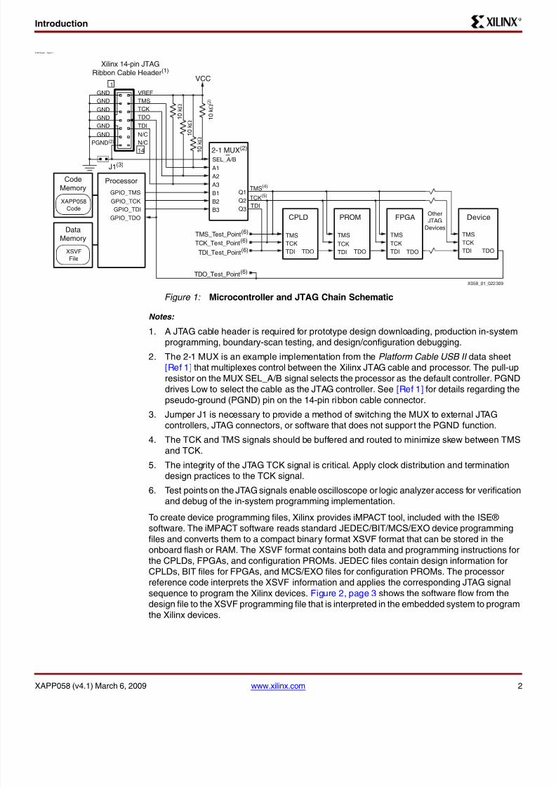
The processor and JTAG chain schematic shown in Figure 1, page 2 can help designersachieve these unprecedented benefits by providing a simple means for programming Xilinx
CPLDs and FPGAs from design information stored in the embedded processor memory space.This design can be modified for remote downloading applications and the included reference C
code can be compiled for the designer’s processor of choice.
Application Note: Xilinx Families
XAPP058 (v4.1) March 6, 2009
Xilinx In-System Programming Using anEmbedded MicrocontrollerContact: Randal Kuramoto
R
8/8/2019 CPLD ISP Programming Thro Micro Controller
http://slidepdf.com/reader/full/cpld-isp-programming-thro-micro-controller 2/23
Introduction
XAPP058 (v4.1) March 6, 2009 www.xilinx.com 2
Notes:
1. A JTAG cable header is required for prototype design downloading, production in-systemprogramming, boundary-scan testing, and design/configuration debugging.
2. The 2-1 MUX is an example implementation from the Platform Cable USB II data sheet[Ref 1] that multiplexes control between the Xilinx JTAG cable and processor. The pull-up
resistor on the MUX SEL_A/B signal selects the processor as the default controller. PGNDdrives Low to select the cable as the JTAG controller. See [Ref 1] for details regarding the
pseudo-ground (PGND) pin on the 14-pin ribbon cable connector.
3. Jumper J1 is necessary to provide a method of switching the MUX to external JTAGcontrollers, JTAG connectors, or software that does not support the PGND function.
4. The TCK and TMS signals should be buffered and routed to minimize skew between TMS
and TCK.
5. The integrity of the JTAG TCK signal is critical. Apply clock distribution and terminationdesign practices to the TCK signal.
6. Test points on the JTAG signals enable oscilloscope or logic analyzer access for verificationand debug of the in-system programming implementation.
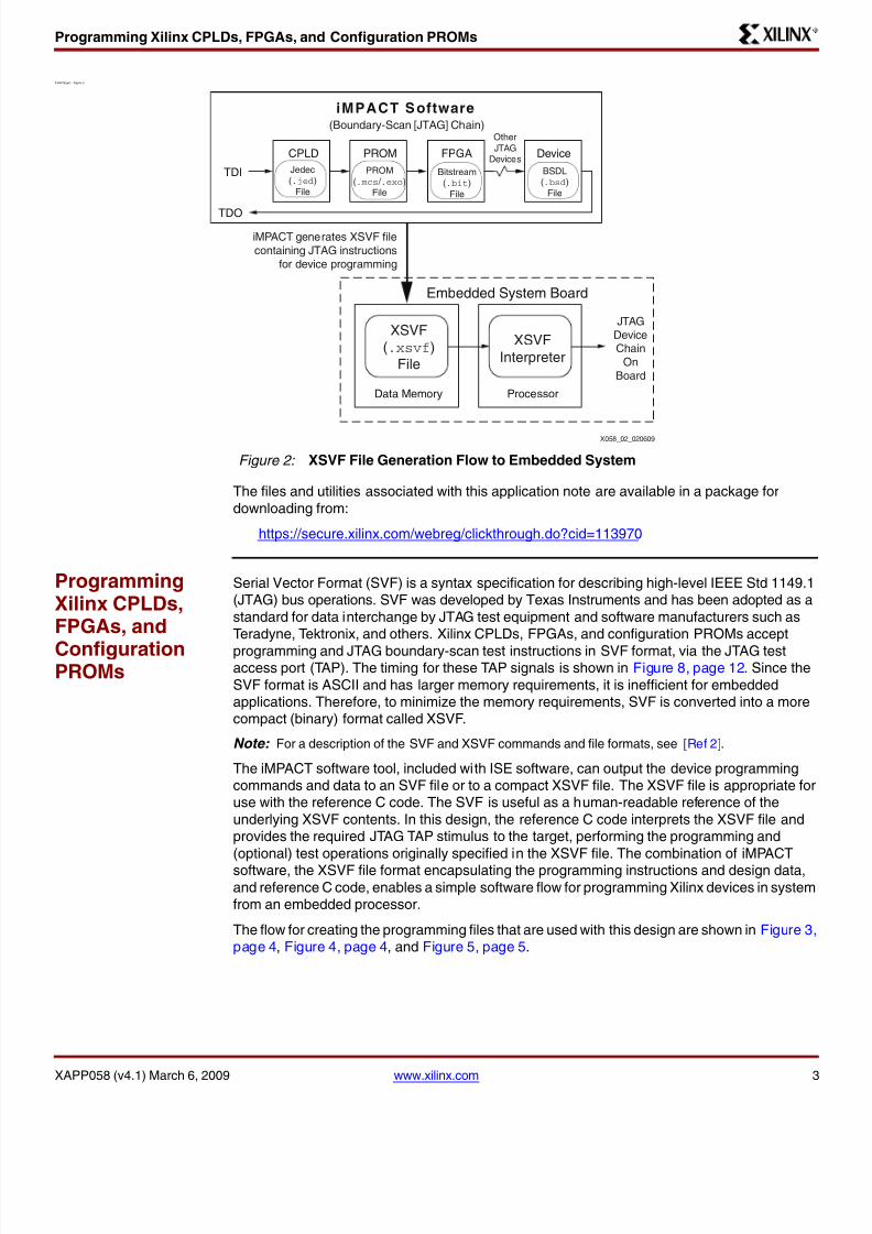
To create device programming files, Xilinx provides iMPACT tool, included with the ISE® software. The iMPACT software reads standard JEDEC/BIT/MCS/EXO device programming
files and converts them to a compact binary format XSVF format that can be stored in the
onboard flash or RAM. The XSVF format contains both data and programming instructions forthe CPLDs, FPGAs, and configuration PROMs. JEDEC files contain design information forCPLDs, BIT files for FPGAs, and MCS/EXO files for configuration PROMs. The processorreference code interprets the XSVF information and applies the corresponding JTAG signal
sequence to program the Xilinx devices. Figure 2, page 3 shows the software flow from thedesign file to the XSVF programming file that is interpreted in the embedded system to program
the Xilinx devices.
X-RefTarget - Figure 1
Figure 1: Microcontroller and JTAG Chain Schematic
TMS
TCK
TDO
TDI
VREF
N/C
N/C
14
1VCC
FPGA
TCK
TDI
TMS
TDO
PROM
TCK
TDI
TMS
TDO
CPLD
TCK
TDI
TMS
TDO
Device
TCK
TDI
TMS
TDO
Processor
GND
GND
GND
GND
GND
GND
Xilinx 14-pin JTAGRibbon Cable Header(1)
J1(3)
CodeMemory
XAPP058Code
GPIO_TMS
GPIO_TCK
GPIO_TDI
GPIO_TDO
DataMemory
XSVF
File
1 0
k Ω
1 0
k Ω
1 0
k Ω
1 0
k Ω ( 2 )
2-1 MUX(2)
SEL_A/B
A1
A2
A3
B1
B2
B3
Q1
Q2
Q3
TMS(4)
TCK(5)
TDI
TMS_Test_Point(6)
TCK_Test_Point(6)
TDI_Test_Point(6)
TDO_Test_Point(6)
Other
JTAGDevices
PGND(2)
X058_01_022309
8/8/2019 CPLD ISP Programming Thro Micro Controller
http://slidepdf.com/reader/full/cpld-isp-programming-thro-micro-controller 3/23
Programming Xilinx CPLDs, FPGAs, and Configuration PROMs
XAPP058 (v4.1) March 6, 2009 www.xilinx.com 3
The files and utilities associated with this application note are available in a package for
downloading from:
https://secure.xilinx.com/webreg/clickthrough.do?cid=113970
ProgrammingXilinx CPLDs,FPGAs, and
ConfigurationPROMs
Serial Vector Format (SVF) is a syntax specification for describing high-level IEEE Std 1149.1(JTAG) bus operations. SVF was developed by Texas Instruments and has been adopted as a
standard for data interchange by JTAG test equipment and software manufacturers such asTeradyne, Tektronix, and others. Xilinx CPLDs, FPGAs, and configuration PROMs accept
programming and JTAG boundary-scan test instructions in SVF format, via the JTAG testaccess port (TAP). The timing for these TAP signals is shown in Figure 8, page 12. Since the
SVF format is ASCII and has larger memory requirements, it is inefficient for embeddedapplications. Therefore, to minimize the memory requirements, SVF is converted into a morecompact (binary) format called XSVF.
Note: For a description of the SVF and XSVF commands and file formats, see [Ref 2].
The iMPACT software tool, included with ISE software, can output the device programmingcommands and data to an SVF file or to a compact XSVF file. The XSVF file is appropriate foruse with the reference C code. The SVF is useful as a human-readable reference of the
underlying XSVF contents. In this design, the reference C code interprets the XSVF file andprovides the required JTAG TAP stimulus to the target, performing the programming and
(optional) test operations originally specified in the XSVF file. The combination of iMPACT
software, the XSVF file format encapsulating the programming instructions and design data,and reference C code, enables a simple software flow for programming Xilinx devices in systemfrom an embedded processor.
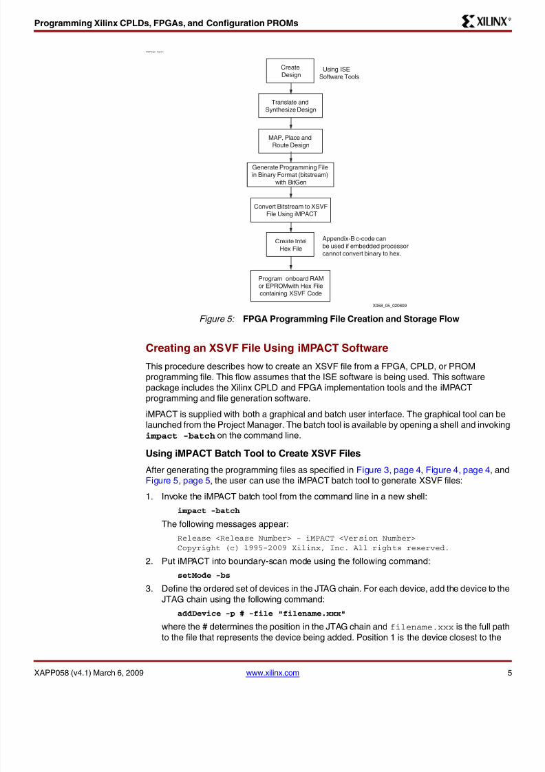
The flow for creating the programming files that are used with this design are shown in Figure 3,page 4, Figure 4, page 4, and Figure 5, page 5.
X-RefTarget - Figure 2
Figure 2: XSVF File Generation Flow to Embedded System
Embedded System Board
iMPACT Software
FPGA Device
TDO
TDI
PROMCPLD
Data Memory Processor
(Boundary-Scan [JTAG] Chain)
Jedec(.jed)
File
PROM
(.mcs / .exo)File
Bitstream(.bit)
File
BSDL(.bsd)
File
iMPACT generates XSVF filecontaining JTAG instructions
for device programming
Other
JTAGDevices
JTAGDeviceChain
OnBoard
XSVF
Interpreter
XSVF(.xsvf)
File
X058_02_020609
8/8/2019 CPLD ISP Programming Thro Micro Controller
http://slidepdf.com/reader/full/cpld-isp-programming-thro-micro-controller 4/23
Programming Xilinx CPLDs, FPGAs, and Configuration PROMs
XAPP058 (v4.1) March 6, 2009 www.xilinx.com 4
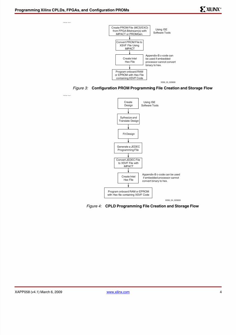
X-RefTarget - Figure 3
Figure 3: Configuration PROM Programming File Creation and Storage Flow
X-RefTarget - Figure 4
Figure 4: CPLD Programming File Creation and Storage Flow
Create PROM File (MCS/EXO)from FPGA Bitstream(s) with
iMPACT or PROMGen.
Create IntelHex File
Program onboard RAMor EPROM with Hex Filecontaining XSVF Code
X058_03_020609
Using ISESoftware Tools
Convert PROM File toXSVF File Using
iMPACT
Appendix-B c-code can
be used if embeddedprocessor cannot convertbinary to hex.
CreateDesign
Sythesize andTranslate Design
Generate a JEDECProgramming File
Create IntelHex File
Program onboard RAM or EPROMwith Hex file containing XSVF Code
X058_04_020609
Using ISESoftware Tools
Fit Design
Convert JEDEC Fileto XSVF File with
iMPACT
Appendix-B c-code can be usedif embedded processor cannot
convert binary to hex.
8/8/2019 CPLD ISP Programming Thro Micro Controller
http://slidepdf.com/reader/full/cpld-isp-programming-thro-micro-controller 5/23
Programming Xilinx CPLDs, FPGAs, and Configuration PROMs
XAPP058 (v4.1) March 6, 2009 www.xilinx.com 5
Creating an XSVF File Using iMPACT Software
This procedure describes how to create an XSVF file from a FPGA, CPLD, or PROMprogramming file. This flow assumes that the ISE software is being used. This software
package includes the Xilinx CPLD and FPGA implementation tools and the iMPACTprogramming and file generation software.
iMPACT is supplied with both a graphical and batch user interface. The graphical tool can belaunched from the Project Manager. The batch tool is available by opening a shell and invokingimpact -batch on the command line.
Using iMPACT Batch Tool to Create XSVF Files
After generating the programming files as specified in Figure 3, page 4, Figure 4, page 4, andFigure 5, page 5, the user can use the iMPACT batch tool to generate XSVF files:
1. Invoke the iMPACT batch tool from the command line in a new shell:
impact -batch
The following messages appear:
Releas
e <Releas
e Number> - iMPACT <Vers
ion Number>Copyright (c) 1995-2009 Xilinx, Inc. All rights reserved.
2. Put iMPACT into boundary-scan mode using the following command:
setMode -bs
3. Define the ordered set of devices in the JTAG chain. For each device, add the device to the
JTAG chain using the following command:
addDevice -p # -file "filename.xxx"
where the # determines the position in the JTAG chain and filename.xxx is the full path
to the file that represents the device being added. Position 1 is the device closest to the
X-RefTarget - Figure 5
Figure 5: FPGA Programming File Creation and Storage Flow
CreateDesign
Translate andSynthesize Design
MAP, Place andRoute Design
Create IntelHex File
Program onboard RAMor EPROMwith Hex Filecontaining XSVF Code
X058_05_020609
Using ISESoftware Tools
Generate Programming Filein Binary Format (bitstream)
with BitGen
Convert Bitstream to XSVFFile Using iMPACT
Appendix-B c-code canbe used if embedded processorcannot convert binary to hex.

8/8/2019 CPLD ISP Programming Thro Micro Controller
http://slidepdf.com/reader/full/cpld-isp-programming-thro-micro-controller 6/23
Programming Xilinx CPLDs, FPGAs, and Configuration PROMs
XAPP058 (v4.1) March 6, 2009 www.xilinx.com 6
initial JTAG TDI input. For a device with a design that needs to be programmed,filename.xxx is the device design file. The file extension for a CPLD design file is .jed.
The file extension for a FPGA design file is .bit. The extension for a PROM file is .mcs or.exo.
PROMs require a special attribute on the adddevice command line that specifies the
PROM type. To add a PROM device to the JTAG chain, use the following command:
addDevice -p # -sprom promtype -file "filename.xxx"
where the # determines the position in the JTAG chain and promtype is xcf32p, xcf16p,xcf08p, xcf04s, xcf02s, xcf01s, xc18v04, xc18v02, xc18v01, or xc18v512. The file attribute,filename.xxx, is the full path to the PROM data file with a .mcs or .exo extension.
For devices not being programmed (e.g., devices from vendors other than Xilinx), add theBSDL file corresponding to the device. A BSDL file typically has the file extension .bsd.
BSDL files are available from the device manufacturer. Xilinx BSDL files are available fromthe download area of the Xilinx website. A device can be added using its BSDL file as
follows:
addDevice -p # -file "filename.bsd"
where the # determines the position in the JTAG chain and filename.bsd is the full pathto the device's BSDL file.
Additional details regarding the adddevice command can be found in the iMPACT onlinemanual.
4. After defining the complete JTAG chain, direct the iMPACT output to an XSVF file using the
following command:
setCable -port xsvf -file "filename.xsvf"
where filename.xsvf is the full path to the output XSVF file.
5. Specify an iMPACT operation on a specific device. iMPACT writes the operation
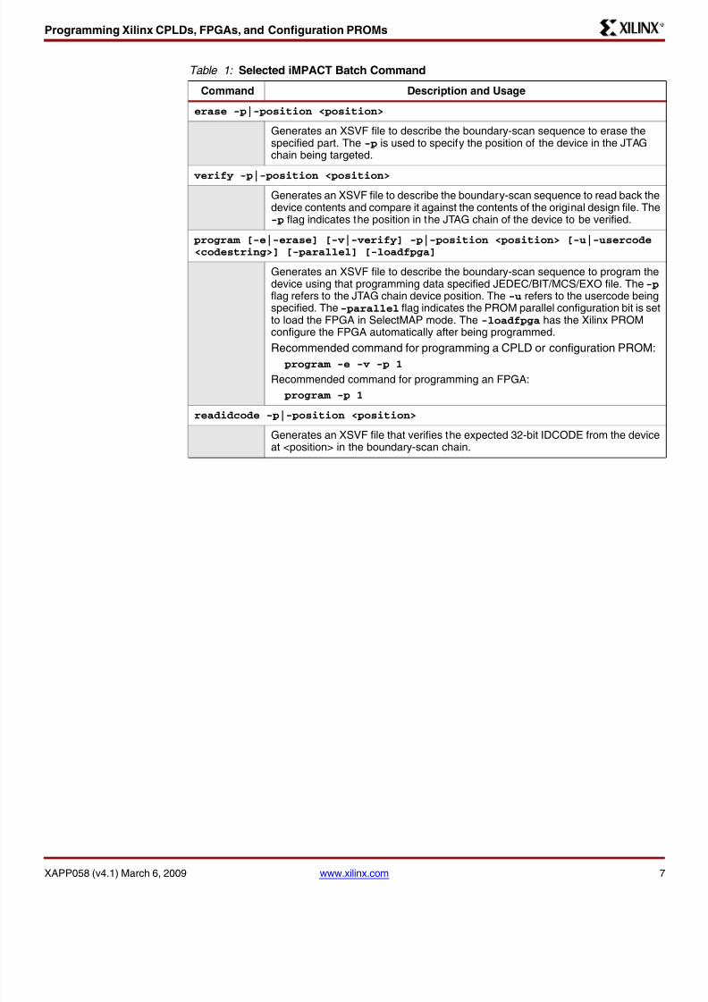
instructions and data to the XSVF file. The most common operations are listed in Table 1.For a detailed list of all operations, see the iMPACT online manual.
6. After specifying an iMPACT operation, close the XSVF file using the following command:
closeCable
7. Quit the iMPACT batch mode using the following command:
quit
8/8/2019 CPLD ISP Programming Thro Micro Controller
http://slidepdf.com/reader/full/cpld-isp-programming-thro-micro-controller 7/23
Programming Xilinx CPLDs, FPGAs, and Configuration PROMs
XAPP058 (v4.1) March 6, 2009 www.xilinx.com 7
Table 1: Selected iMPACT Batch Command
Command Description and Usage
erase -p|-position <position>
Generates an XSVF file to describe the boundary-scan sequence to erase thespecified part. The -p is used to specify the position of the device in the JTAGchain being targeted.
verify -p|-position <position>
Generates an XSVF file to describe the boundary-scan sequence to read back thedevice contents and compare it against the contents of the original design file. The-p flag indicates the position in the JTAG chain of the device to be verified.
program [-e|-erase] [-v|-verify] -p|-position <position> [-u|-usercode<codestring>] [-parallel] [-loadfpga]
Generates an XSVF file to describe the boundary-scan sequence to program thedevice using that programming data specified JEDEC/BIT/MCS/EXO file. The -p flag refers to the JTAG chain device position. The -u refers to the usercode beingspecified. The -parallel flag indicates the PROM parallel configuration bit is setto load the FPGA in SelectMAP mode. The -loadfpga has the Xilinx PROMconfigure the FPGA automatically after being programmed.
Recommended command for programming a CPLD or configuration PROM: program -e -v -p 1
Recommended command for programming an FPGA:
program -p 1
readidcode -p|-position <position>
Generates an XSVF file that verifies the expected 32-bit IDCODE from the deviceat <position> in the boundary-scan chain.
8/8/2019 CPLD ISP Programming Thro Micro Controller
http://slidepdf.com/reader/full/cpld-isp-programming-thro-micro-controller 8/23
Programming Xilinx CPLDs, FPGAs, and Configuration PROMs
XAPP058 (v4.1) March 6, 2009 www.xilinx.com 8
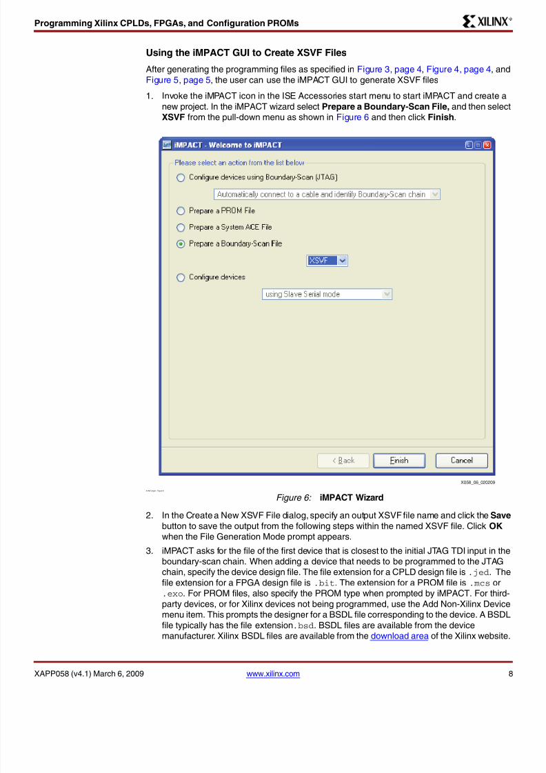
Using the iMPACT GUI to Create XSVF Files
After generating the programming files as specified in Figure 3, page 4, Figure 4, page 4, and
Figure 5, page 5, the user can use the iMPACT GUI to generate XSVF files
1. Invoke the iMPACT icon in the ISE Accessories start menu to start iMPACT and create a
new project. In the iMPACT wizard select Prepare a Boundary-Scan File, and then selectXSVF from the pull-down menu as shown in Figure 6 and then click Finish.
2. In the Create a New XSVF File dialog, specify an output XSVF file name and click the Save
button to save the output from the following steps within the named XSVF file. Click OK when the File Generation Mode prompt appears.
3. iMPACT asks for the file of the first device that is closest to the initial JTAG TDI input in theboundary-scan chain. When adding a device that needs to be programmed to the JTAGchain, specify the device design file. The file extension for a CPLD design file is .jed. The
file extension for a FPGA design file is .bit. The extension for a PROM file is .mcs or.exo. For PROM files, also specify the PROM type when prompted by iMPACT. For third-
party devices, or for Xilinx devices not being programmed, use the Add Non-Xilinx Devicemenu item. This prompts the designer for a BSDL file corresponding to the device. A BSDL
file typically has the file extension.bsd. BSDL files are available from the devicemanufacturer. Xilinx BSDL files are available from the download area of the Xilinx website.
X-RefTarget - Figure 6
Figure 6: iMPACT Wizard
X058_06_020209
8/8/2019 CPLD ISP Programming Thro Micro Controller
http://slidepdf.com/reader/full/cpld-isp-programming-thro-micro-controller 9/23
Programming Xilinx CPLDs, FPGAs, and Configuration PROMs
XAPP058 (v4.1) March 6, 2009 www.xilinx.com 9
If no BSDL file is available, iMPACT can create a BSDL file given the device's JTAGinstruction register length in bits.
4. If there is more than one device in the chain, then add each device to the chain via thefollowing procedure. To add a device at the end of the chain, r ight-click in the iMPACT
window to the right of the last device in the chain. iMPACT presents a menu of items foradding a device to the chain. For Xilinx devices, choose the Add Xilinx Device menu item,
and specify the .bit, .jed, .mcs, or .bsd file corresponding to the Xilinx device. Forother devices, choose the Add Non-Xilinx Device menu item, and specify the device's
BSDL file or create a BSDL for the device. Repeat this step until all devices are specified inthe chain.
5. After the complete boundary-scan chain is specified, select the target device (it should behighlighted) and right-click to see the available operations for the device. Select the
operation(s) to be written to the XSVF file in the order needed (Figure 7). Therecommended operation and operation attributes follow for specific device types:
♦ CPLDs and PROMs: Operation-->Program with the Erase before Programming and
Verify attributes selected.
♦ FPGAs: Operation-->Program (The Erase Before Programming and Verify attributes of the program operation are not supported for FPGA devices.)
6. Output→ XSVF File → Stop writing to the XSVF File to exit and stop writing to the XSVF
file.
Storing the XSVF File in an EPROM
To store the XSVF file in an EPROM, the binary XSVF file must be converted to an Intel Hex orsimilar PROM format file. Most embedded processor development system software
automatically converts included binary files to the appropriate format. For systems without thiscapability, reference C code to perform this conversion can be found in “Appendix B: Binary to
Intel Hex Translator,” page 20.
X-RefTarget - Figure 7
Figure 7: Add Device
X058_07_021709
8/8/2019 CPLD ISP Programming Thro Micro Controller
http://slidepdf.com/reader/full/cpld-isp-programming-thro-micro-controller 10/23
Hardware Design
XAPP058 (v4.1) March 6, 2009 www.xilinx.com 10
Software Limitations
iMPACT can generate XSVF files only for Xilinx programmable logic devices and Xilinx JTAG insystem programmable PROMs. Designers should verify that the development software can
create an XSVF file for the specific device to be programmed.
Hardware
Design
As shown in Figure 1, page 2, the reference design requires:
• A microprocessor
• Enough memory to contain both the compiled C-code and the XSVF file
• Three processor-controlled outputs for the JTAG TCK, TMS, and TDI signals
• One processor-readable input for the JTAG TDO signal
Hardware Design for the JTAG Chain
Interfacing the processor to the board-level JTAG signals is typically done in one of two ways.In some implementations, the JTAG signals are connected to general-purpose I/O (GPIO) pinson the processor. Figure 1, page 2 shows an example of this type of implementation. In other
implementations, memory-mapped registers are used to drive or capture the JTAG signals.Both solutions are equally effective. Either way, four I/O pins are required: three output pins to
drive the JTAG TCK, TMS, and TDI signals, and one input pin to read the JTAG TDO signal.
The JTAG bus is a multipurpose bus. It is often used for board-level boundary-scan test, cable
based downloading of prototype designs for programmable logic devices, and as an accesspoint for debugging programmable logic or processors. For this reference design, the processor
uses the JTAG bus to program programmable logic devices or JTAG in-system programmablePROMs.
Because of the multipurpose nature of the JTAG bus, a hardware implementation that enablesdifferent JTAG masters to control the JTAG chain is essential. A hardware solution must allow
for the appropriate JTAG master to control the JTAG chain when needed, and must avoid signalcontention on the JTAG bus from multiple JTAG masters. Several different kinds of
implementations can satisfy these requirements.
The example JTAG chain schematic in Figure 1, page 2 includes a multiplexer that enablesswitching between the processor and an external JTAG cable, which can also act as master ofthe JTAG bus (by default, the processor has control). This example is derived from themultiplexer example in [Ref 1]. The implementation takes advantage of the Xilinx Platform
Cable USB II PGND function to automatically switch control to the cable during iMPACTsoftware operations. PGND is driven Low during iMPACT software operations. See [Ref 1] for
details regarding the PGND function and software that supports the PGND function. Themultiplexer example in Figure 1, page 2 is enhanced with a critical jumper (J1) that enables
external JTAG masters to control the bus when the external JTAG hardware or software doesnot support a PGND-like function.
The JTAG chain can span long distances and connect many devices on a board. Specialattention to the design and layout of the JTAG TCK signal are required to ensure good signal
integrity at the TCK pin of all devices in the JTAG chain. The use of board-level clock designand routing guidelines that require proper buffering, termination, and layout, are essential.Because the TMS signal is also routed to all devices in the JTAG chain, the TMS signal must be
designed and routed such that skew is minimized between TMS and TCK.
Multiple devices with different I/O voltage requirements can be connected to the JTAG chain.
For devices with configurable JTAG I/O voltage support, choose an I/O voltage level that iscompatible with the rest of the JTAG chain. Some devices can require the insertion of level
translators between the device's JTAG TAP pins and the rest of the JTAG chain to ensurecompatible signal levels.
Refer to [Ref 3] for additional JTAG hardware design recommendations.
8/8/2019 CPLD ISP Programming Thro Micro Controller
http://slidepdf.com/reader/full/cpld-isp-programming-thro-micro-controller 11/23
Hardware Design
XAPP058 (v4.1) March 6, 2009 www.xilinx.com 11
Memory Requirements
Typical implementations of the reference design require a processor with significant memoryresources for code storage, run-time memory, and XSVF file storage.
The memory requirement for code storage depends on the processor instruction set andcompiler. A reasonable code size estimate can be obtained by compiling the reference C code
for a select processor. As a rough reference, the xapp058_example.exe can be compiled toa 17 KB file without run-time libraries.
The run-time memory requirement is dominated by temporary buffers for storing the bit valuesfor one JTAG shift operation. By default, the temporary buffers are defined in a data structure
that is stored on the stack—the default size for the data structure is approximately 50 KB.Optimizations to the reference C code can be made to either store the temporary buffers in alocation other than the stack or to shorten the length of the temporary buffers. The lengths of
the temporary buffers are defined by the MAX_LEN attribute. See the readme.txt in thereference design package and the lenval.h file for information about the temporary buffers.
Memory is also required to store the XSVF file. Typically, the entire XSVF file is stored within thelocal memory space of the embedded processor. The XSVF file depends on the target device
type, on the architecture of the JTAG chain, and on the selected operations for the targetdevice. To obtain an accurate XSVF file size estimate, a sample design must be created for the
target device within the target JTAG chain, and the corresponding XSVF file must be createdusing the desired iMPACT operations.
Table 2 lists sample iMPACT 10.1.03 XSVF file sizes for typical programming operations onrepresentative Xilinx devices (in single-device JTAG chains). For sample CPLDs, the Erase
Before Programming and Verify options are used when generating the XSVF using the desirediMPACT operations. For sample PROMs, the XSVF file is generated from a full-sized MCS filethat matches the PROM size using the iMPACT Program operation, including the Erase Before
Programming and Verify options. For sample FPGAs, the XSVF file is generated from anuncompressed bitstream using the iMPACT Program operation without options.
Some techniques can be used to reduce XSVF file storage requirements. File compressiontechniques can be used to compress a stored XSVF file (see [Ref 4]).
Alternatively, the reference C code can be modified to wait for pieces of the XSVF that aretransferred as smaller blocks to the embedded system for remote update applications.
Table 2: Sample XSVF File Sizes
Device Type File Size (Bytes)
XC9536 45,624
XC95288 726,170
XC9536XL 39,453
XC95288XL 136,305
XC2C32A 11,442
XC2C512 210,791
XCF04S 3,222,351
XCF32P 23,630,691
XC3S700A 344,468
XC5VLX50 1,582,011
8/8/2019 CPLD ISP Programming Thro Micro Controller
http://slidepdf.com/reader/full/cpld-isp-programming-thro-micro-controller 12/23
Firmware Design
XAPP058 (v4.1) March 6, 2009 www.xilinx.com 12
FirmwareDesign
This reference design is provided with C code that can be ported and compiled to an embeddedprocessor. The main function of the C code is to interpret a given XSVF file and to drive the
JTAG bus with corresponding signal sequences. See [Ref 2] for details of the commands in theXSVF file.
TAP Timing
Figure 8 shows the timing relationships of the TAP signals. Table 3, page 13 provides example
TAP timing parameters for the XC9500 CPLD. See the data sheet for each device in the JTAGchain to determine the JTAG TAP timing parameters for each device.
Key JTAG TAP timing considerations include:
• A JTAG device requires a minimum TCK period (TCKMIN).
• A JTAG device samples TMS and TDI on the rising edge of TCK. The device requires TMSand TDI to be valid for a minimum setup time (TMSS/TDIS) before the rising edge of TCK
and for a minimum hold time (TMSH/TDIH) after the rising edge of TCK.
• A JTAG device outputs a new TDO value by a maximum time (TDOV) after the falling edgeof TCK.
See the data sheets of the devices in the JTAG chain for these timing parameters.
The reference C code controls the primary JTAG TAP signals. The speed at which the code
toggles the JTAG TAP signals is dependent on the processor speed. Often, the toggle rate fromthe processor is sufficiently slow and the device timing is sufficiently fast that no timing
violations occur. To ensure proper TAP timing in the reference C code implementation, thedesigner should:
• Check the data sheet of each device in the JTAG chain for the TCKMIN period.
The longest TCKMIN period of all devices in the JTAG chain is the minimum TCK
period for the entire chain. Check that the minimum TCK period driven from thereference C code implementation in the processor is greater than or equal to the
minimum TCK period for the entire chain (in other words, the TCK can not run fasterthan the slowest device in the chain).
• Check the data sheet for each device in the JTAG chain for minimum TMS setup time.
The longest TMS setup time is the minimum TMS setup time for the entire JTAG chain.
Check that the minimum time from a TMS transition to the next rising edge of TCK isgreater than or equal to the minimum TMS setup time for the entire chain. Similarly,
check the minimum TMS hold time, which is the time from the rising-edge of TCK to thetransition of TMS to a new value.
X-RefTarget - Figure 8
Figure 8: Test Access Port Timing
TCKMIN
TMSS TMSH
TDIS
TDOV TDOXZTDOZX
TDIH
TCK
TMS
TDI
TDO
X058_08_021709
8/8/2019 CPLD ISP Programming Thro Micro Controller
http://slidepdf.com/reader/full/cpld-isp-programming-thro-micro-controller 13/23
Firmware Design
XAPP058 (v4.1) March 6, 2009 www.xilinx.com 13
• Check the TDI setup and hold times for each device in the chain.
The timing checks for TDI and TDO are different than the timing checks for TCK andTMS because TDI and TDO are daisy-chained from one device to the next in the JTAG
chain. The processor-driven TDI must meet the TDI setup and hold time for the firstdevice in the JTAG chain. The TDO output from the first device must meet the TDI
setup and hold for the second device in the JTAG chain, and so on. Finally, the TDOoutput from the last device in the JTAG chain should not be sampled before the
maximum TDOV time (maximum time from the falling edge of TCK to when TDO outputdata is valid).
If the JTAG TAP timing is violated, additional delays must be added in the reference code. Todelay signal transitions or TCK toggle rates, add a delay in the setPort function within thePORTS.C file. To delay the sample timing of TDO, add a delay in the readTDOBit function withinthe PORTS.C file.
Note: Some compilers remove empty loops. Delay loops must be implemented such that they are
retained during code compilation.
Table 3 lists the XC9500 timing parameters for the TAP waveforms shown in Figure 8, page 12.
For other device families, see the device family data sheet for TAP timing characteristics.
Special Cases for the XSVF File and XSVF Interpreter
As mentioned previously, XSVF is a compact, binary version of the de facto standard SVF fileformat. The SVF file contains deterministic JTAG commands and data. For most cases, theXSVF is a near identical reflection of a corresponding SVF file—though in a more compact
form. However, for two special cases, the XSVF is created with a slight modification oroptimization from a corresponding SVF file.
Exception Handling for XC9500/XL/XV Programming
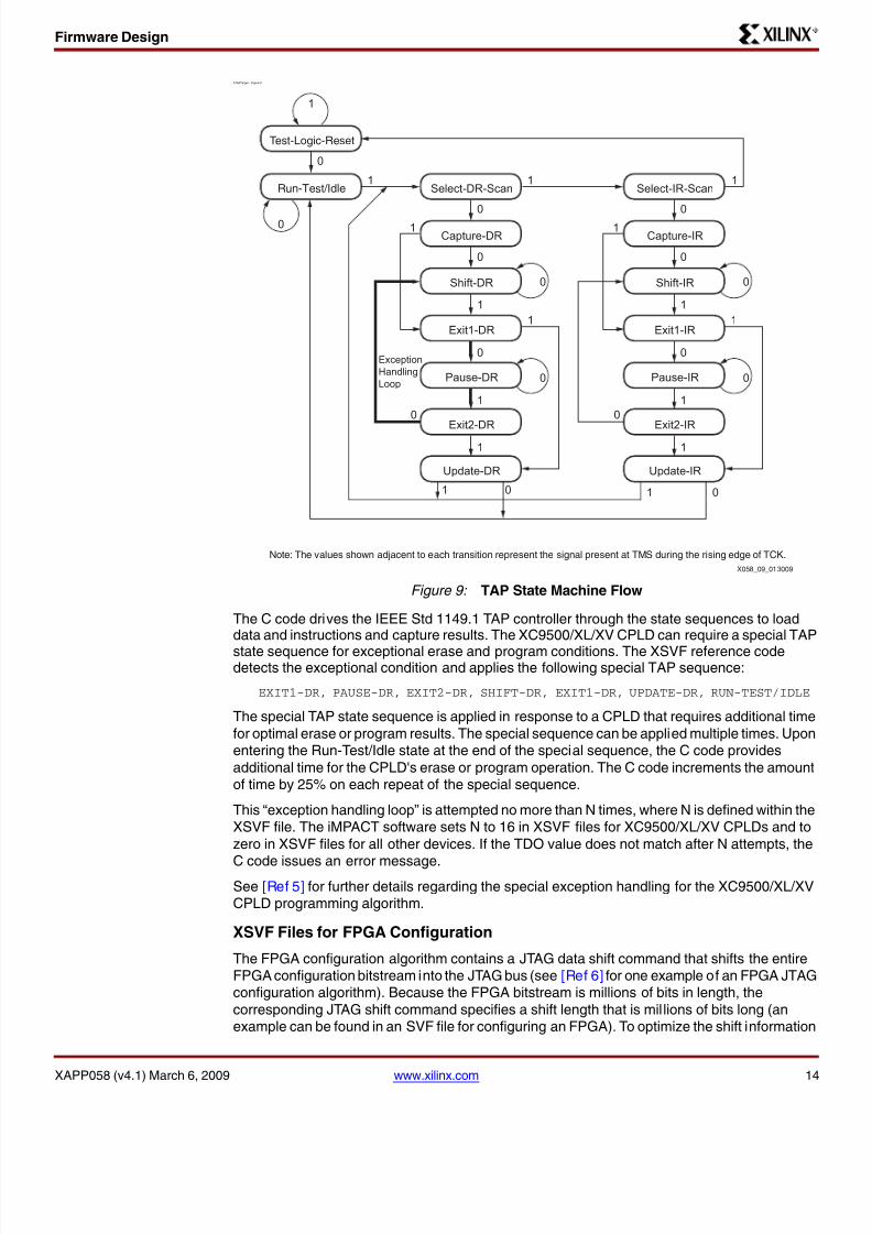
Figure 9 shows the state diagram for the internal device programming state machine, asdefined by the IEEE Std 1149.1.
Table 3: XC9500 Test Access Port Timing Parameters (ns)
Symbol Parameter Min Max
TCKMIN TCK Minimum Clock Period 100
TMSS TMS Setup Time 10
TMSH TMS Hold Time 10
TDIS TDI Setup Time 15
TDIH TDI Hold Time 25
TDOZX TDO Float-to-Valid Delay 35
TDOXZ TDI Valid-to-Float Delay 35
TDOV TDO Valid Delay 35
8/8/2019 CPLD ISP Programming Thro Micro Controller
http://slidepdf.com/reader/full/cpld-isp-programming-thro-micro-controller 14/23
Firmware Design
XAPP058 (v4.1) March 6, 2009 www.xilinx.com 14
The C code drives the IEEE Std 1149.1 TAP controller through the state sequences to loaddata and instructions and capture results. The XC9500/XL/XV CPLD can require a special TAP
state sequence for exceptional erase and program conditions. The XSVF reference codedetects the exceptional condition and applies the following special TAP sequence:
EXIT1-DR, PAUSE-DR, EXIT2-DR, SHIFT-DR, EXIT1-DR, UPDATE-DR, RUN-TEST/IDLE
The special TAP state sequence is applied in response to a CPLD that requires additional time
for optimal erase or program results. The special sequence can be applied multiple times. Uponentering the Run-Test/Idle state at the end of the special sequence, the C code provides
additional time for the CPLD's erase or program operation. The C code increments the amountof time by 25% on each repeat of the special sequence.
This “exception handling loop” is attempted no more than N times, where N is defined within theXSVF file. The iMPACT software sets N to 16 in XSVF files for XC9500/XL/XV CPLDs and to
zero in XSVF files for all other devices. If the TDO value does not match after N attempts, the
C code issues an error message.See [Ref 5] for further details regarding the special exception handling for the XC9500/XL/XVCPLD programming algorithm.
XSVF Files for FPGA Configuration
The FPGA configuration algorithm contains a JTAG data shift command that shifts the entireFPGA configuration bitstream into the JTAG bus (see [Ref 6] for one example of an FPGA JTAGconfiguration algorithm). Because the FPGA bitstream is millions of bits in length, the
corresponding JTAG shift command specifies a shift length that is millions of bits long (anexample can be found in an SVF file for configuring an FPGA). To optimize the shift information
X-RefTarget - Figure 9
Figure 9: TAP State Machine Flow
Select-DR-Scan
Capture-DR
Shift-DR
Exit1-DR
Pause-DR
Exit2-DR
Update-DR
0
0
1
0
1
0
Run-Test/Idle
0
0
1 1 1
0
1
0
1
Exception
Handling
Loop
1
1
1 0
Select-IR-Scan
Capture-IR
Shift-IR
Exit1-IR
Pause-IR
Exit2-IR
Update-IR
0
0
0
1 0
1
0
0
1
0
1
1
1
X058_09_013009
Test-Logic-Reset
Note: The values shown adjacent to each transition represent the signal present at TMS during the rising edge of TCK.
8/8/2019 CPLD ISP Programming Thro Micro Controller
http://slidepdf.com/reader/full/cpld-isp-programming-thro-micro-controller 15/23
Firmware Implementation
XAPP058 (v4.1) March 6, 2009 www.xilinx.com 15
for an embedded processor, an XSVF file is generated with the long bitstream shift representedas multiple XSVF commands—each command defines a short segment of the original
bitstream. This effectively reduces the run-time buffer requirements in the embedded code. Seethe readme.txt in the reference design package for corresponding buffer length
requirements in the reference C code.
Firmware
Implementation
This section outlines the basic steps to implementing the hardware and reference C code in an
embedded processor.
Step 1: Define the JTAG Chain and Programming Tasks
First, identify the set of devices in the JTAG chain. Then, identify target device(s) within theJTAG chain that the embedded processor will program. For devices not programmed by the
embedded processor, obtain the BSDL files from the device manufacturer.
Step 2: Determine XSVF File Size
After the target devices to be programmed are identified, the XSVF file size can be determined.
For each of the target devices to be programmed, obtain a sample design file. Then, follow theiMPACT software instructions for generating an XSVF file that performs the desired operations
on the target devices.
Step 3: Determine XSVF File Location
After determining the XSVF file size, determine the location where the XSVF file is stored. TheXSVF can be statically stored in non-volatile memory when the embedded processor is the
primary configuration source for the Xilinx device. Alternatively, the XSVF can be dynamicallytransferred to a RAM location in the embedded system for remote update applications. The
storage location of the XSVF file determines the method the XSVF interpreter (reference Ccode) uses to retrieve the XSVF file data.
Step 4: Planning Processor Resources
Sufficient processor memory resources must be available to store code, store the XSVF file,and run code. The XSVF file and its storage location defines one memory requirement for the
embedded system. In addition, the reference code size determines another set of memoryrequirements for code storage and code execution memory. Finally, the run-time memoryrequirements must also be considered.
The reference code size depends on the processor instruction set and compiler. Compiling thereference code with the preferred compiler for the embedded processor provides an estimate
for the code size.
Run-time requirements are primarily determined by the size of the SXsvfInfo data structure
defined in the micro.c file. One instance of the SXsvfInfo data structure is created at run timeon the stack (the stack location of the SXsvfInfo data structure instance can be changed
through modifications in the micro.c code). The size of the SXsvfInfo data structure isdominated by the instances of the lenVal data structures within the SXsvfInfo data structure.
There are up to seven instances of the lenVal data structure within the SXsvfInfo data structure.
The lenVal defines buffers for bit values used in the JTAG shift operations. The size of the lenValbuffers are defined by the MAX_LEN parameter in the lenval.h file. By default, the
MAX_LEN is 7,000 bytes. If possible, do not change the default MAX_LEN value; this defaultvalue allows margin for large JTAG shift operations in future devices. If required, the MAX_LEN
parameter can be reduced to optimize the SXsvfInfo data structure size. See the readme.txtand lenval.h files for guidelines on reducing the MAX_LEN value.
A legacy feature of the XSVF are special XSVF compression commands that optimized theXSVF for programming XC9500/XL/XV CPLDs. These XSVF compression commands are not
supported in the XSVF output from the iMPACT software. If the implementation is not requiredto support legacy XSVF files that contain special XSVF compression commands, then remove
8/8/2019 CPLD ISP Programming Thro Micro Controller
http://slidepdf.com/reader/full/cpld-isp-programming-thro-micro-controller 16/23
Verifying and Tuning the Design Implementation
XAPP058 (v4.1) March 6, 2009 www.xilinx.com 16
the #define for XSVF_SUPPORT_COMPRESSION in micro.c. Removal of the #define forthe XSVF_SUPPORT_COMPRESSION can reduce the SXsvfInfo data structure size by over
40% and can reduce the code size by a modest amount.
Step 5: Design Processor I/O
Determine the hardware method that the processor uses to control and read the JTAG bus
signals. Typical implementations use processor GPIO or memory-mapped registers. Seedescriptions of example implementations in the “Hardware Design for the JTAG Chain” section
Step 6: Design JTAG Bus Control Scheme
Because the JTAG bus is typically shared between the embedded processor and external JTAG
controllers, such as the Xilinx iMPACT software and Xilinx cables, a JTAG bus multiplexingscheme is advised. See Figure 1, page 2 for an example JTAG bus multiplexing scheme that
provides selectable control of the JTAG bus from either the embedded processor or externalJTAG hardware and software.
Add test points on the JTAG bus for verification and debug access.
Step 7: Porting Reference C Code
The key functions, whose implementations are required to be ported to the embedded
processor, are located in the ports.c file. The functions include:♦ setPort: sets a JTAG output signal (TCK, TMS, or TDI) to a specified value. The
setPort implementation depends on the design of the processor I/O for the outputJTAG signals.
♦ readTDOBit: reads (i.e., samples) the JTAG input signal (TDO) value. The
implementation of the readTDOBit function must return the JTAG input signal value.The implementation depends on the design of the processor I/O.
♦ readByte: returns the next byte from the XSVF file. The micro.c code calls the
readByte function in order to read successive bytes from the XSVF file. Theimplementation of the readByte function must also remember the last read position ofthe XSVF file. The implementation depends on the location of the XSVF file. For
example, when the XSVF file is stored in memory, the readByte implementation
typically uses a pointer that returns the next byte from an array location in memory.
♦ waitTime: consumes (i.e., waits) for at least the specified number of microseconds(waiting for longer is okay), specified by an integer parameter value. The minimum
waiting time is required to allow devices to complete certain operations, such as a
PROM erase operation. The implementation must satisfy two requirements:
- The waitTime function must interpret the integer parameter value as a time in
microseconds.
- The waitTime function must also interpret the integer parameter value as anumber of TCK pulses that must be applied during the waiting time (pulsing TCK
for a number of times that is greater than the number specified in the integerparameter is okay). The minimum TCK pulses are used to clock certain deviceoperations, such as the FPGA startup sequence.
See the waitTime function in the ports.c file for example implementations thatsatisfy the requirements.
Verifying andTuning theDesignImplementation
This section outlines the basic steps for verifying the correctness of the reference design
implementation.
Step 1: Verify JTAG Chain
Connect the Xilinx cable to the JTAG chain, and use the iMPACT software to apply desiredboundary-scan operations to target devices in the JTAG chain. The iMPACT software
8/8/2019 CPLD ISP Programming Thro Micro Controller
http://slidepdf.com/reader/full/cpld-isp-programming-thro-micro-controller 17/23
Verifying and Tuning the Design Implementation
XAPP058 (v4.1) March 6, 2009 www.xilinx.com 17
operations should match those operations that are to be performed by the embeddedprocessor.
In the case of an iMPACT software failure, check the following:
• Check that the Xilinx cable is the selected master controller for the JTAG chain (i.e., checkfor correct JTAG bus multiplexer configuration).
• Check that the JTAG chain is defined correctly in the iMPACT boundary-scan window.
• Check the TCK signal integrity. The TCK edges should rise or fall monotonically withoutglitches at the TCK pin of each device.
Step 2: Verify XSVF Files
While iMPACT is connected to the JTAG chain via a Xilinx cable, follow the instructions given inthe “Creating an XSVF File Using iMPACT Software” section. Generate a minimal XSVF that
performs only the Get Device ID operation on one target device in the JTAG chain. This deviceID XSVF file can be used to validate basic functionality of the reference code implementation.
Also, generate the XSVF file that performs the desired programming operation on the targetdevice in the JTAG chain.
After generating the XSVF files, use iMPACT to validate them on the JTAG chain using thefollowing procedure.
1. Restart iMPACT and create a new project for boundary-scan configuration.
2. Add one of the XSVF files to the boundary-scan window.
3. Select the XSVF file icon in the boundary-scan window.
4. Right-click on the XSVF file icon and invoke the Execute SVF/XSVF menu item to executethe XSVF file through the Xilinx cable to the JTAG chain.
5. Verify that the XSVF file execution is successful. To verify each XSVF file, repeat thisprocedure for each XSVF file.
In the case of an iMPACT software XSVF execution failure, check the following:
• Check that the Xilinx cable is the selected master controller for the JTAG chain (i.e., check
for correct JTAG bus multiplexer configuration).
• Check that the JTAG chain is defined correctly in the iMPACT boundary-scan window.
Step 3: PORTS.C waitTime Calibration
Calibrating the implementation of the waitTime function within the ports.c file is critical for
success of XSVF file operations in the embedded system. The reference design packageincludes files for calibrating the waitTime function implementation. See thereadme_ports_c_waittime_calibration.txt file in the reference design package fordetails about the calibration method and associated files.
Here are some general guidelines for calibrating the waitTime function (these also apply to theinstructions in the “Step 4: JTAG TAP Timing Verification” section:
• Use an oscilloscope to probe the JTAG bus. The oscilloscope provides a visual of the
calibration results.• Run the calibration files using non-debug code to ensure that the calibrated timing
measurements are accurate for the production version of the embedded system.
• Check the shorter calibration timing tests to ensure proper timing for shorter wait times.
• Check the longer calibration timing tests to ensure timing calculations or loops in the
waitTime function implementation do not overflow and result in unexpectedly short waittimes.
If the calibration tests show that the waitTime function does not meet the requirements, then tryor check the following:
8/8/2019 CPLD ISP Programming Thro Micro Controller
http://slidepdf.com/reader/full/cpld-isp-programming-thro-micro-controller 18/23
Troubleshooting
XAPP058 (v4.1) March 6, 2009 www.xilinx.com 18
• To increase the resulting wait time, increase the multiplication factor for the number of TCKpulses to be applied.
• If delay loops are used, check that the compiler is not removing empty loops.
Step 4: JTAG TAP Timing Verification
Using one of the waitTime calibration XSVF files (or the Get Device ID XSVF file that wasgenerated in “Step 2: Verify XSVF Files,” page 17), and with the oscilloscope probes on the
JTAG signals, execute the XSVF file and check the timing of the JTAG signal transitions. Thebasic JTAG TAP signal timing requirements are outlined in the TAP Timing section.
Tips for checking the JTAG TAP signal timing:
• Use a waitTime calibration XSVF for checking the TCK period as TCK toggles during the
wait time.
• Use a waitTime calibration XSVF for checking the timing of a TMS edge to the followingTCK rising edge.
• Use the Get Device ID XSVF for checking the timing of a TDI edge to the following TCKrising edge.
• If the JTAG TAP timing verification results in timing violations, then try the following:
♦ For TCK periods or setup times that are too short, insert a delay at the beginning of
the setPort function.
♦ For a readTDOBit function that reads before TDO is valid, insert a delay at thebeginning of the readTDOBit function.
Note: Some compilers remove empty loops. When inserting delays, ensure an implementation that is
not removed by a compiler optimization.
Step 5: Basic JTAG Chain Test with the Embedded Processor
Start testing the embedded implementation of the reference code using a small XSVF file. The
Get Device ID XSVF, created in “Step 2: Verify XSVF Files,” page 17, is a small XSVF file fromiMPACT that tests for a valid device ID return value. Prepare the embedded system with the Get
Device ID XSVF file. Then execute the Get Device ID XSVF file to test the operation of theembedded reference code implementation.
If the Get Device ID XSVF fails, try the following checks:
• Check that the XSVF file works when run via iMPACT through a Xilinx cable to the JTAG
chain.
• Check for TCK signal integrity.
• Check the return value from TDO. If the return value pattern does not match the expected
device ID pattern, check the mismatch between the returned and expected value for clues
After the Get Device ID XSVF is verified to work successfully, try an XSVF file that programs the
target device.
TroubleshootingThe following suggestions can be helpful in troubleshooting this design:
• If using a multiplexing scheme to switch between the processor and other JTAG controlsources, check that the multiplexer is configured correctly for the JTAG control source
being tested.
• Use iMPACT to execute the XSVF file(s) through a Xilinx cable to the JTAG chain.
• Generate a simple XSVF that only checks the IDCODE of the target device to test basicfunctionality of the hardware and software.
• Narrow the problem area by generating and executing separate XSVF files for the erase,blank check, program, and verify operations.
8/8/2019 CPLD ISP Programming Thro Micro Controller
http://slidepdf.com/reader/full/cpld-isp-programming-thro-micro-controller 19/23
Alternate Embedded Programming Solutions
XAPP058 (v4.1) March 6, 2009 www.xilinx.com 19
• Program the device from iMPACT via a download cable to verify basic hardware functionality.
• Check for embedded memory collisions (i.e., check that there is sufficient XSVF storagememory and run-time memory to execute the XSVF without corruption).
AlternateEmbedded
ProgrammingSolutions
The XSVF-based reference design provided in this application note is the most fully supportedembedded configuration reference design for the Xilinx products. It supports all Xilinx FPGA,
CPLD, and in-system programmable PROM devices. It is the only Xilinx embeddedprogramming reference design that has full support for Xilinx XC9500/XL/XV CPLDs.
Alternate embedded programming solutions are available that can satisfy specific situations,including:
• The Embedded JTAG ACE Player application note [Ref 7] describes an HDL referencedesign that is suitable for implementation in an FPGA. The accompanying reference
design describes how to configure FPGAs, CoolRunner-II CPLDs, or Xilinx in-systemprogrammable PROMs through a JTAG bus using the SVF-derived ACE file (from System
ACE CF).
• For third-party flash devices without a JTAG TAP, the Spartan-3A Starter Kit includes a
variety of flash programmer demonstration designs.
Conclusion Xilinx CPLDs, FPGAs, and JTAG in-system programmable PROMs are easily programmed by
an embedded processor. Because they are IEEE Std 1149.1 compliant, system and device testfunctions can also be controlled by the embedded processor. This capability opens new
possibilities for upgrading designs in the field, creating user-specific features, and remotedownloading of CPLD/FPGA programs.
8/8/2019 CPLD ISP Programming Thro Micro Controller
http://slidepdf.com/reader/full/cpld-isp-programming-thro-micro-controller 20/23
Appendix A: C-Code Listing
XAPP058 (v4.1) March 6, 2009 www.xilinx.com 20
Appendix A:C-Code Listing
The following files contain the C source code used to read an XSVF file and output theappropriate Test Access Port control bits:
C-Code Files
• lenval.c — This file contains routines for using the lenVal data structure. The lenValdata structure is a buffer that holds a set of bit values used in a low-level JTAG shift
operation.
• micro.c — This file contains the main function call for reading an XSVF file from
memory, interpreting the XSVF file commands, and driving the JTAG signals.
• ports.c — This file contains the routines to output values on the JTAG ports, to read theTDO bit, and to read a byte of XSVF data from memory.
Header Files
• lenval.h — This file contains a definition of the lenVal data structure and externprocedure declarations for manipulating objects of type lenVal. The lenVal structure is a
byte oriented type used to store an arbitrary length binary value.
• micro.h — This file contains the declaration for the main entry point to the XSVFinterpreter and definitions of possible return values.
• ports.h — This file contains extern declarations for providing stimulus to the JTAG ports
To compile this C code for an embedded processor, only four functions within the ports.c fileneed to be modified:
• setPort — Sets a JTAG output signal (TCK, TMS, or TDI) to a specified value.
• readTDOBit — Reads the JTAG TDO signal value.
• readByte — Reads a byte of data from the XSVF file.
• waitTime — Consumes/waits for at least the specified amount of time and pulses the TCKsignal while waiting.
Appendix B:Binary to IntelHex Translator
This appendix contains C code that can be used to convert XSVF files to Intel Hex format for
downloading to an EPROM programmer. Most embedded processor code developmentsystems can output Intel Hex for included binary files; for those systems, the following code isnot needed. However, designers can use the following C code if the development system they
are using does not have Intel Hex output capability.
#include <stdio.h>
#define RECORD_SIZE0x10/* Size of a record. */
#define BUFFER_SIZE 128
/*** Local Global Variables ***/
static char *line, buffer[BUFFER_SIZE];
static FILE *infile;
/*** Extern Functions Declarations ***/
extern char hex( int c );
extern void puthex( int val, int digits );
/*** Program Main ***/
main( int argc, char *argv[] )
{
int c=1, address=0;
8/8/2019 CPLD ISP Programming Thro Micro Controller
http://slidepdf.com/reader/full/cpld-isp-programming-thro-micro-controller 21/23
Appendix B: Binary to Intel Hex Translator
XAPP058 (v4.1) March 6, 2009 www.xilinx.com 21
int sum, i;
i=0;
/*** First argument - Binary input file ***/
if (!(infile = fopen(argv[++i],"rb"))) {
fprintf(stderr, “Error on open of file %s\n”,argv[i]);
exit(1);
}
/*** Read the file character by character ***/
while (c != EOF) {
sum = 0;
line = buffer;
for (i=0; i<RECORD_SIZE && (c=getc(infile)) != EOF; i++) {
*line++ = hex(c>>4);
*line++ = hex(c);
sum += c; /* Checksum each character. */
}
if (i) {
sum += address >> 8;/* Checksum high address byte.*/
sum += address & 0xff;/* Checksum low address byte.*/
sum += i; /* Checksum record byte count.*/
line = buffer; /* Now output the line! */
putchar(':');
puthex(i,2); /* Byte count. */
puthex(address,4); /* Do address and increment */
address += i; /* by bytes in record. */
puthex(0,2); /* Record type. */
for(i*=2;i;i--) /* Then the actual data. */
putchar(*line++);
puthex(0-sum,2); /* Checksum is 1 byte 2's comp.*/
printf("\n");
}
}
printf(":00000001FF\n");/* End record. */
}
/* Return ASCII hex character for binary value. */
char
hex( int c )
{
if((c &= 0x000f)<10)
c += '0';
else
c += 'A'-10;
return((char) c);
}
/* Put specified number of digits in ASCII hex. */
void
puthex( int val, int digits )
{
if (--digits)
puthex(val>>4,digits);
putchar(hex(val & 0x0f));
}
8/8/2019 CPLD ISP Programming Thro Micro Controller
http://slidepdf.com/reader/full/cpld-isp-programming-thro-micro-controller 22/23
References
XAPP058 (v4.1) March 6, 2009 www.xilinx.com 22
References 1. DS593, Platform Cable USB II
2. XAPP503, SVF and XSVF File Formats for Xilinx Devices .
3. XAPP104, A Quick JTAG ISP Checklist
4. http://www.zlib.net, zlib compression library
5. XAPP067, Using Serial Vector Format Files to Program XC9500/XL/XV Devices In-System
6. UG191, Virtex-5 FPGA Configuration User Guide
7. XAPP424, Embedded JTAG ACE Player
RevisionHistory
The following table shows the revision history for this document.
Date Version Revision
01/15/01 3.0 Revised Xilinx release.
06/25/04 3.1 Minor changes made.
03/11/05 3.2 Updated for Platform Flash PROMs.
10/01/07 4.0 • Updated template.
• Updated document for ISE iMPACT 9.2i support.
• Other minor edits and changes made.
01/13/09 4.0.1 Updated link to reference design files.
03/06/09 4.1 • Updated link to reference design files.
• Added new Figure 2, page 3.
• Updated Figure 1, page 2, Figure 3, page 4, Figure 4, page 4,Figure 5, page 5, and Figure 8, page 12.
• Removed Figures 8–15 and 17.
• Updated Table 1, page 7, Table 2, page 11, and Table 3, page 13.
• Removed original Tables 1, 2, 3, and 5.
• Updated steps in “Using iMPACT Batch Tool to Create XSVF Files,”page 5 and “Using the iMPACT GUI to Create XSVF Files,” page 8.
• Removed sections: Modifications for Other Applications, XC4000 andSpartan/Spartan-XL Family Programming Algorithm, Virtex Seriesand Spartan-II/3/3E/3A Programming Algorithm, CoolRunnerProgramming Algorithm, XC18V00 PROM Programming Algorithm,memory map, port map, XC9500/XL/XV Programming Algorithm,JTAG Instruction Summary, and File Merge Utility sections.
• Added sections: “Hardware Design for the JTAG Chain,” page 10,“XSVF Files for FPGA Configuration,” page 14, “Verifying and Tuningthe Design Implementation,” page 16, “Special Cases for the XSVFFile and XSVF Interpreter,” page 13, and “Firmware Implementation,”page 15.
• Renamed 'Debugging Suggestions' section “Troubleshooting,”page 18.
• Added references [Ref 3], [Ref 4], [Ref 5], [Ref 6], and [Ref 7].
• Moved Appendix-A into “Firmware Design,” page 12 section.
8/8/2019 CPLD ISP Programming Thro Micro Controller
http://slidepdf.com/reader/full/cpld-isp-programming-thro-micro-controller 23/23
Notice of Disclaimer
Notice ofDisclaimer
Xilinx is disclosing this Application Note to you “AS-IS” with no warranty of any kind. ThisApplication Note is one possible implementation of this feature, application, or standard, and is
subject to change without further notice from Xilinx. You are responsible for obtaining any rightsyou may require in connection with your use or implementation of this Application Note. XILINX
MAKES NO REPRESENTATIONS OR WARRANTIES, WHETHER EXPRESS OR IMPLIED,STATUTORY OR OTHERWISE, INCLUDING, WITHOUT LIMITATION, IMPLIEDWARRANTIES OF MERCHANTABILITY, NONINFRINGEMENT, OR FITNESS FOR A
PARTICULAR PURPOSE. IN NO EVENT WILL XILINX BE LIABLE FOR ANY LOSS OF DATA,LOST PROFITS, OR FOR ANY SPECIAL, INCIDENTAL, CONSEQUENTIAL, OR INDIRECT
DAMAGES ARISING FROM YOUR USE OF THIS APPLICATION NOTE.