RECORDS OF REVISION - Future Electronics · 【Note3】 Lamp frequency of inverter may produce...
22
Transcript of RECORDS OF REVISION - Future Electronics · 【Note3】 Lamp frequency of inverter may produce...

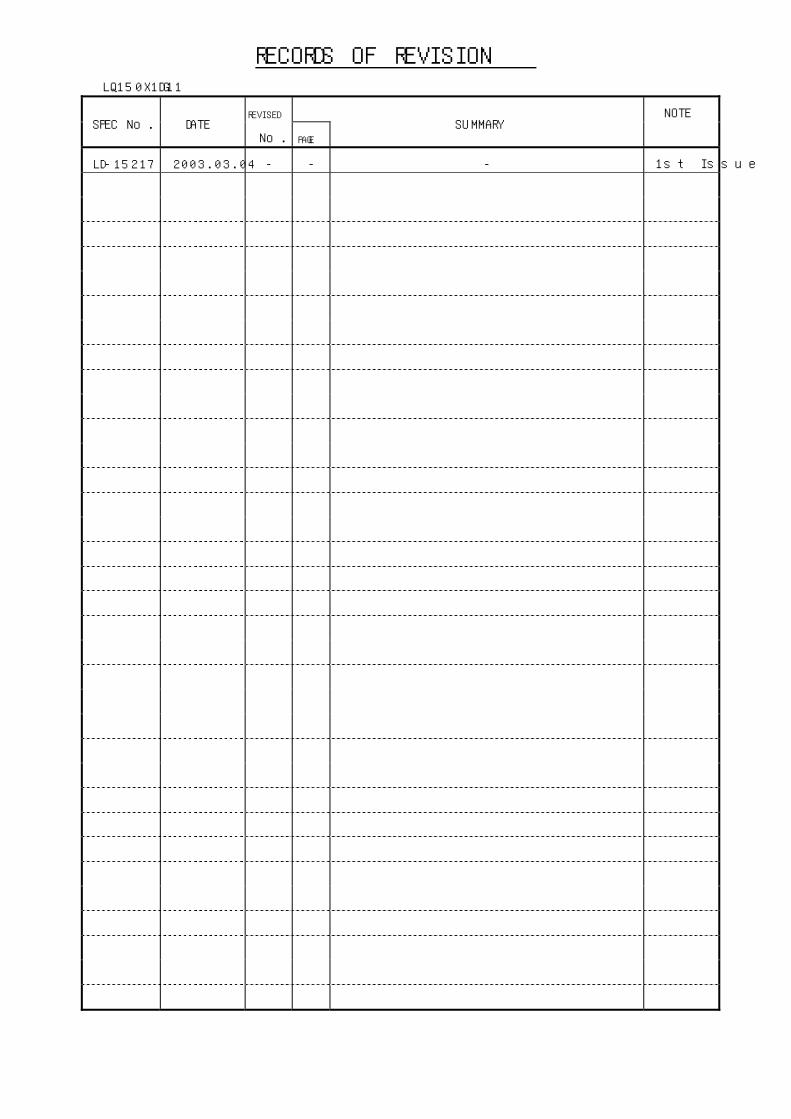
RECORDS OF REVISION LQ150X1DG11
REVISED SPEC No. DATE
No. PAGE
SUMMARY NOTE
LD-15217 2003.03.04 - - - 1st Issue

LD-15217-1
1. Application
This specifications applies to a color TFT-LCD module, LQ150X1DG11.
◎These specification sheets are the proprietary product of SHARP CORPORATION(”SHARP) and include
materials protected under copyright of SHARP. Do not reproduce or cause any third party to reproduce them in
any form or by any means, electronic or mechanical, for any purpose, in whole or in part, without the express
written permission of SHARP .
◎The device listed in these specification sheets was designed and manufactured for use in OA equipment .
◎In case of using the device for applications such as control and safety equipment for transportation(aircraft,
trains, automobiles, etc. ), rescue and security equipment and various safety related equipment which require
higher reliability and safety, take into consideration that appropriate measures such as fail-safe functions and
redundant system design should be taken .
◎Do not use the device for equipment that requires an extreme level of reliability, such as aerospace applications,
telecommunication equipment(trunk lines), nuclear power control equipment and medical or other equipment for
life support .
◎SHARP assumes no responsibility for any damage resulting from the use of the device which does not comply
with the instructions and the precautions specified in these specification sheets .
◎Contact and consult with a SHARP sales representative for any questions about this device .
2. Overview
This module is a color active matrix LCD module incorporating amorphous silicon TFT (Thin Film Transistor).
It is composed of a color TFT-LCD panel, driver ICs, control circuit, power supply circuit and a back light unit.
Graphics and texts can be displayed 1024×3×768 dots on a panel with 262,144 colors by supplying 36 bit data
signals(6 bit×2pixel×RGB), four timing signals, +5V DC supply voltage for TFT-LCD panel driving and supply
voltage for back light .
It is a wide viewing-angle-module (Vertical viewing angle:120°Horizontal viewing angle:140°).
Input signal timing conform with 75Hz mode of VESA standard.

LD-15217-2
3. Mechanical Specifications
Parameter Specifications Unit
Display size 38 (Diagonal) cm
15.0 (Diagonal) inch
Active area 304.1 (H)×228.1 (V) mm
Pixel format 1024 (H)×768 (V) pixel
(1 pixel=R+G+B dots)
Pixel pitch 0.297 (H)×0.297 (V) mm
Pixel configuration R,G,B vertical stripe
Display mode Normally white
Unit outline dimensions *1 331.3(W)×257.9 (H)×15.9(D) mm
Mass 1300 (max.) g
Surface treatment
Anti-glare and hard-coating 2H
(Haze value = 28)
*1.Note: excluding back light cables .
The thickness of module (D) doesn’t contain the projection .
*2.Outline dimension is shown in Fig.1
LD-15217-3
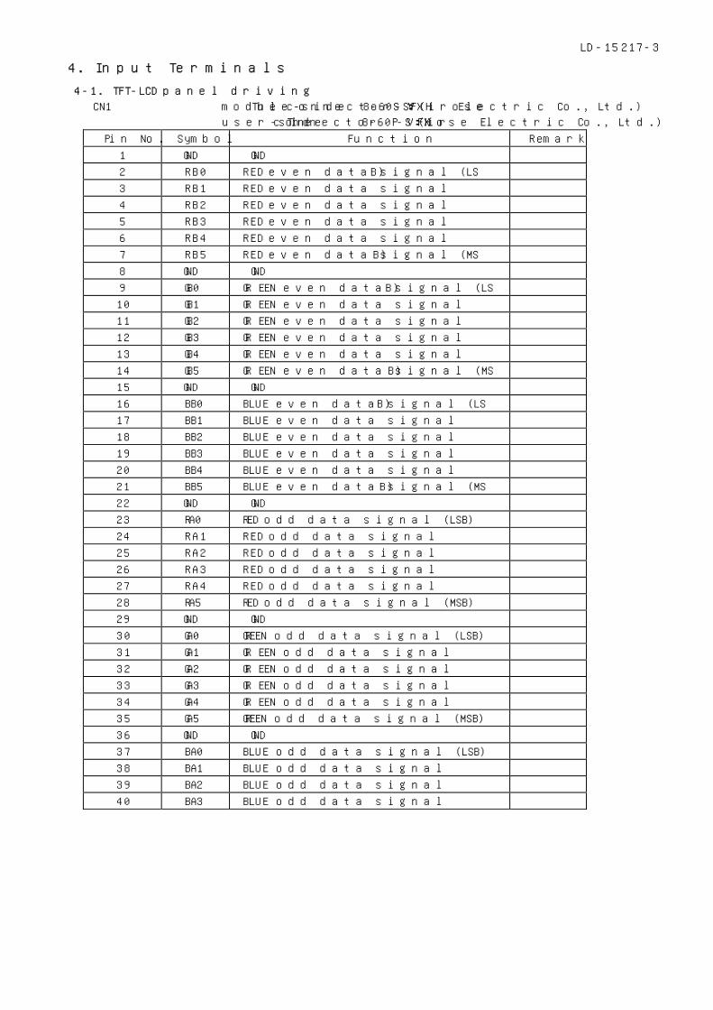
4. Input Terminals
4-1. TFT-LCD panel driving
CN1 The module-side connector :FX8-60S-SV (Hirose Electric Co., Ltd.)
The user-side connector :FX8-60P-SV (Hirose Electric Co., Ltd.)
Pin No. Symbol Function Remark
1 GND GND
2 RB0 RED even data signal (LSB)
3 RB1 RED even data signal
4 RB2 RED even data signal
5 RB3 RED even data signal
6 RB4 RED even data signal
7 RB5 RED even data signal (MSB)
8 GND GND
9 GB0 GREEN even data signal (LSB)
10 GB1 GREEN even data signal
11 GB2 GREEN even data signal
12 GB3 GREEN even data signal
13 GB4 GREEN even data signal
14 GB5 GREEN even data signal (MSB)
15 GND GND
16 BB0 BLUE even data signal (LSB)
17 BB1 BLUE even data signal
18 BB2 BLUE even data signal
19 BB3 BLUE even data signal
20 BB4 BLUE even data signal
21 BB5 BLUE even data signal (MSB)
22 GND GND
23 RA0 RED odd data signal (LSB)
24 RA1 RED odd data signal
25 RA2 RED odd data signal
26 RA3 RED odd data signal
27 RA4 RED odd data signal
28 RA5 RED odd data signal (MSB)
29 GND GND
30 GA0 GREEN odd data signal (LSB)
31 GA1 GREEN odd data signal
32 GA2 GREEN odd data signal
33 GA3 GREEN odd data signal
34 GA4 GREEN odd data signal
35 GA5 GREEN odd data signal (MSB)
36 GND GND
37 BA0 BLUE odd data signal (LSB)
38 BA1 BLUE odd data signal
39 BA2 BLUE odd data signal
40 BA3 BLUE odd data signal
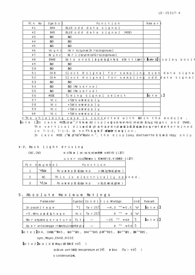
LD-15217-4
Pin No. Symbol Function Remark
41 BA4 BLUE odd data signal
42 BA5 BLUE odd data signal (MSB)
43 GND GND
44 GND GND
45 GND GND
46 Vsync Vertical synchronous signal
47 Hsync Horizontal synchronous signal
48 ENAB Data enable signal (Signal to settle the display position) 【Note 1】
49 GND GND
50 GND GND
51 CKB Clock B signal for sampling even data signal
52 CKA Clock A signal for sampling odd data signal
53 GND GND
54 GND GND (Reserve)
55 GND GND (Reserve)
56 MODE Timing signal select 【Note 1】
57 Vcc +5V power supply
58 Vcc +5V power supply
59 Vcc +5V power supply
60 Vcc +5V power supply
※The shielding case is connected with GND in the module .
【Note 1】In case MODE is fixed “Low”, the display start timing is determined by Vsync and ENAB.
The vertical display start position and horizontal display start position are determined as described
in 7-1-2, 7-1-3. Do not keep ENAB “high” during operation.
In case MODE is fixed “High” or “Open”, the display start timing is determined by only ENAB.
4-2. Back light driving
CN2,CN3 The module-side connector : BHR-03VS-1(JST)
The user-side connector : SM02(8.0)B-BHS-1(JST)
Pin no. symbol Function
1 VHIGH Power supply for lamp (High voltage side)
2 NC This is electrically opened.
3 VLOW Power supply for lamp (Low voltage side)
5. Absolute Maximum Ratings
Parameter Symbol Condition Ratings Unit Remark
Input voltage VI Ta=25℃ -0.3 ~+5.5 V 【Note1】
+5.0V supply voltage Vcc Ta=25℃ 0 ~ + 6 V
Storage temperature Tstg - -25 ~ +60 ℃ 【Note2】
Operating temperature (Ambient) Topa - 0 ~ +50 ℃
【Note1】CKA, CKB, RA0~RA5, GA0~GA5, BA0~BA5, RB0~RB5, GB0~GB5, BB0~BB5,
Hsync, Vsync, ENAB, MODE
【Note2】Humidity:95%RH Max. ( Ta≦40℃ )
Maximum wet-bulb temperature at 39℃ or less ( Ta>40℃ )
No condensation.

LD-15217-5
6. Electrical Characteristics
6-1. TFT-LCD panel driving Ta=25℃
Parameter Symbol Min. Typ. Max. Unit Remark
Vcc Supply voltage Vcc +4.5 +5.0 +5.5 V 【Note1】
Current dissipation Icc - 300 450 mA 【Note2】
Permissive input ripple voltage VRF - - 100 mVp-p Vcc=+5.0V
Input voltage (Low) VIL GND - 0.6 V 【Note3】
Input voltage (High) VIH 2.6 Vcc V 【Note3】
Input current (Low) IIL - - 10 μA VI=GND【Note3】
- - 400 μA VI=GND【Note4】
Input current (High) - - 10 μA VI=Vcc【Note3】
IIH
- - 600 μA VI=Vcc【Note4】
※ 3.3(v) logic is recommended as
t1
4.5VVcc
data
Vcc
data
t4
2.7V 2.7V
input signals .
【Note1】
On-off conditions for supply voltage
0<t1≦10ms
t4≧1s
Vcc-dip conditions
1) 2.7V≦Vcc<4.5V Vcc
td
2.7V
4.5V
td≦10ms
2) Vcc<2.7V
Vcc-dip conditions should also follow the
on-off conditions
【Note2】 Typical current situation : 16-gray-bar pattern. R G B
G S 0
R G B
G S 4
R G B
G S 8
R G B
G S 5 6
R G B
G S 6 0. . . .
Vcc=+5.0V,
Gray scale : GS(4n)
n=0~15
The explanation of each gray scale ,GS(4n), is described
below section (8).
【Note3】CKA, CKB, RA0~RA5, GA0~GA5, BA0~BA5, RB0~RB5, GB0~GB5, BB0~BB5,
Hsync, Vsync, ENAB
To control ASIC
20kΩ 3.3kΩ
10kΩ
Vcc Internal Power Supply (3.3V)
MODE
【Note4】MODE
Input circuit of MODE is
shown in right figure.
LD-15217-6
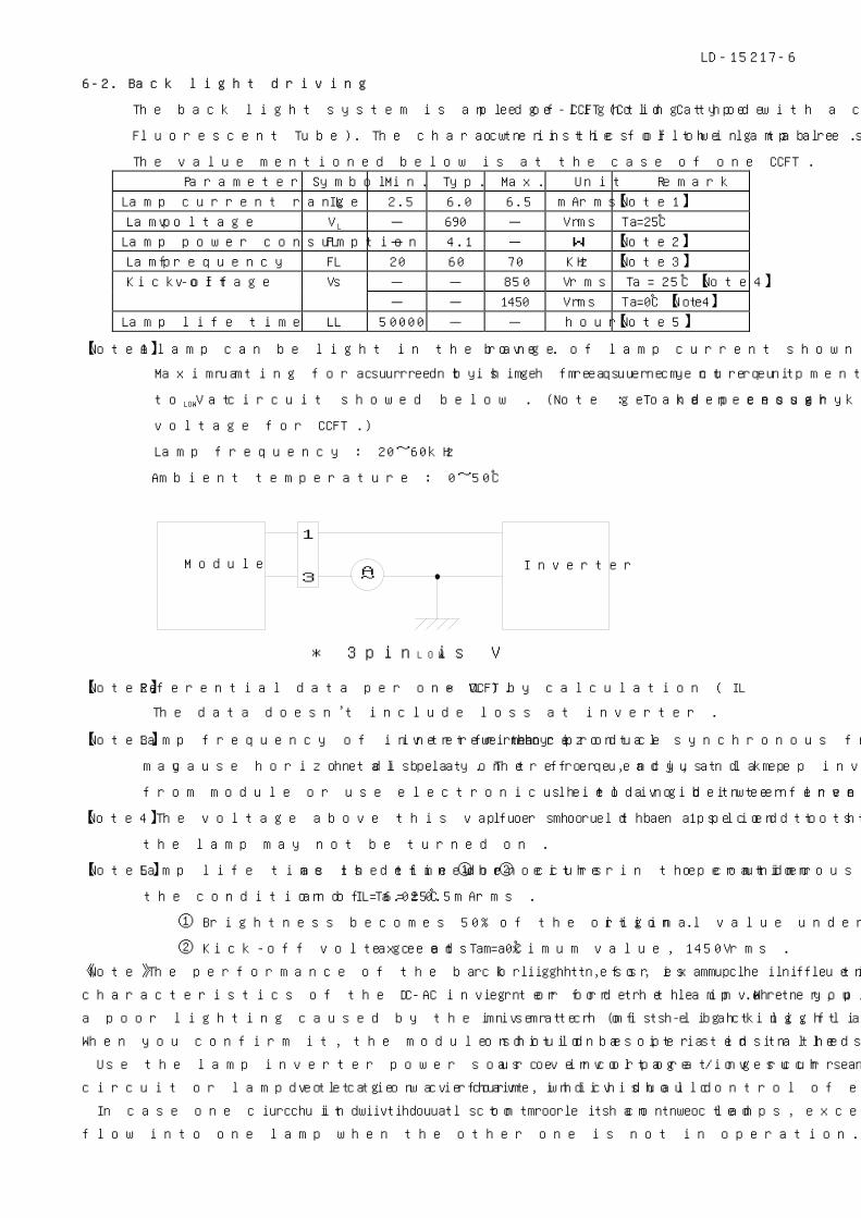
6-2. Back light driving
The back light system is an edge-lighting type with a couple of CCFT (Cold Cathode
Fluorescent Tube). The characteristics of the lamp are shown in the following table .
The value mentioned below is at the case of one CCFT .
Parameter Symbol Min. Typ. Max. Unit Remark
Lamp current range IL 2.5 6.0 6.5 mArms 【Note1】
Lamp voltage VL - 690 - Vrms Ta=25℃
Lamp power consumption PL - 4.1 - W 【Note2】
Lamp frequency FL 20 60 70 KHz 【Note3】
Kick-off voltage Vs - - 850 Vrms Ta=25℃【Note4】
- - 1450 Vrms Ta=0℃【Note4】
Lamp life time LL 50000 - - hour 【Note5】
【Note1】 A lamp can be light in the range of lamp current shown above .
Maximum rating for current is measured by high frequency current measurement equipment connected
to VLOW at circuit showed below . (Note : To keep enough kick-off voltage and necessary steady
voltage for CCFT .)
Lamp frequency : 20~60kHz
Ambient temperature : 0~50℃
Module
1
3InverterA
~
* 3pin is V LOW
【Note2】 Referential data per one CCFT by calculation ( IL × VL ) .
The data doesn’t include loss at inverter .
【Note3】 Lamp frequency of inverter may produce interference with horizontal synchronous frequency, and this
may cause horizontal beat on the display. Therefore, adjust lamp frequency, and keep inverter as far as
from module or use electronic shielding between inverter and module to avoid interference.
【Note4】The voltage above this value should be applied to the lamp for more than 1 second to startup. Otherwise
the lamp may not be turned on .
【Note5】 Lamp life time is defined as the time when either ① or ② occurs in the continuous operation under
the condition of Ta=25℃ and IL=6.0±0.5mArms .
① Brightness becomes 50% of the original value under standard condition .
② Kick-off voltage at Ta=0℃ exceeds maximum value, 1450Vrms .
《Note》The performance of the back light, for example life time or brightness, is much influenced by the
characteristics of the DC-AC inverter for the lamp .When you design or order the inverter, please make sure that
a poor lighting caused by the mismatch of the back light and the inverter (miss-lighting, flicker, etc.) never occurs.
When you confirm it, the module should be operated in the same condition as it is installed in your instrument.
Use the lamp inverter power source incorporating such safeguard as overvoltage / overcurrent protective
circuit or lamp voltage waveform detection circuit, which should have individual control of each lamp.
In case one circuit without such individual control is connected to more than two lamps, excessive current may
flow into one lamp when the other one is not in operation.
LD-15217-7
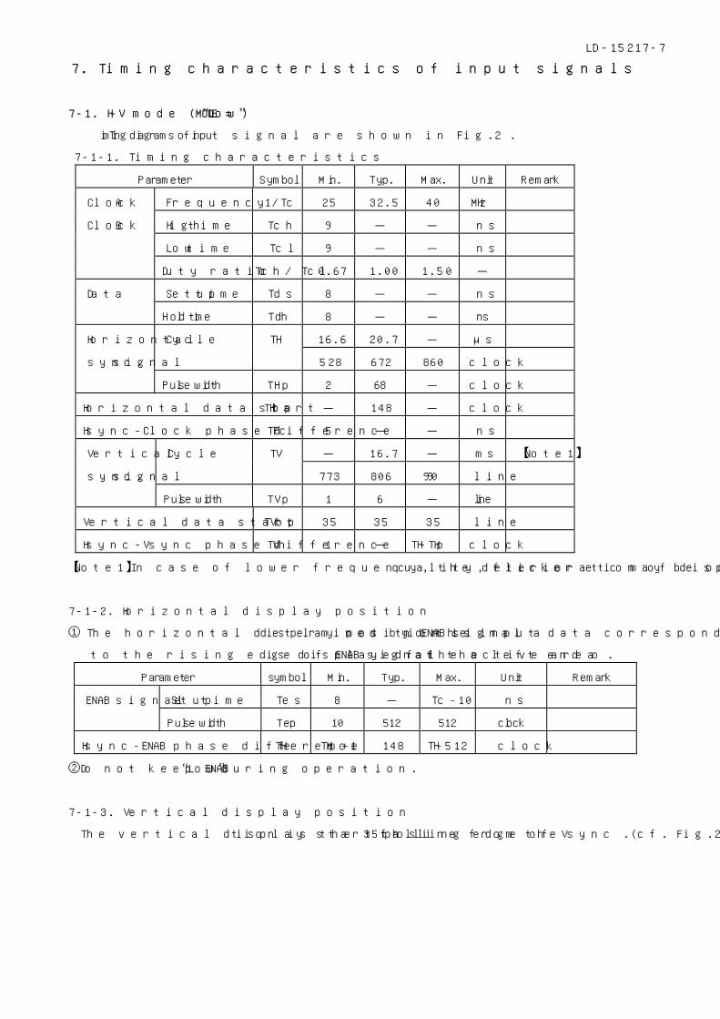
7. Timing characteristics of input signals
7-1. H-V mode (MODE = “Low” )
Timing diagrams of input signal are shown in Fig.2 .
7-1-1. Timing characteristics
Parameter Symbol Min. Typ. Max. Unit Remark
Clock A Frequency 1/Tc 25 32.5 40 MHz
Clock B High time Tch 9 - - ns
Low time Tcl 9 - - ns
Duty ratio Tch/ Tcl 0.67 1.00 1.50 -
Data Setup time Tds 8 - - ns
Hold time Tdh 8 - - ns
Horizontal Cycle TH 16.6 20.7 - μs
sync. signal 528 672 860 clock
Pulse width THp 2 68 - clock
Horizontal data start THbp - 148 - clock
Hsync-Clock phase difference TFc 5 - - ns
Vertical Cycle TV - 16.7 - ms 【Note1】
sync. signal 773 806 990 line
Pulse width TVp 1 6 - line
Vertical data start TVbp 35 35 35 line
Hsync-Vsync phase difference TVh 1 - TH-THp clock
【Note1】In case of lower frequency, the deterioration of display quality, flicker etc may be occurred .
7-1-2. Horizontal display position
① The horizontal display position is determined by ENAB signal and the input data corresponding
to the rising edge of ENAB signal is displayed at the left end of the active area .
Parameter symbol Min. Typ. Max. Unit Remark
ENAB signal Setup time Tes 8 - Tc-10 ns
Pulse width Tep 10 512 512 clock
Hsync-ENAB phase difference THe THp+1 148 TH-512 clock
②Do not keep ENAB “Low” during operation.
7-1-3. Vertical display position
The vertical display start position is the 35th line from the falling edge of Vsync .(cf. Fig.2)

Horizontal sync signal (Hsync)
Clock signal A
Clock signal B
THc
C0* C1*
THp
Number of data
TH
Data A (RA0~RA5,GA0~GA5 BA0~BA5)
0.6V
DA511 DA512 INVALID INVALID
THbp
DB511 DB512 INVALID INVALIDData B (RB0~RB5,GB0~GB5 BB0~BB5)
2.6V
VENAB Signal
THe
0.6V
Tds Tdh
DA1 DA2 DA3 2.6V
DB1 DB2 DB3 2.6V
Tch TclTc
2.6V
0.6V
0.6V
0.6V
0.6V
2.6VTes
Tep
DA1 DA2 DA3
DB1 DB2 DB3
Fig.2 Input Signal Waveforms(H-V Mode)
Data signal (RA0~RA5,GA0~GA5,BA0~BA5) (RB0~RB5,GB0~GB5,BB0~BB5)
DH1 DH2 DH3 DH765 DH768INVALID INVALID
Horizontal sync signal (Hsync)
TVh
TVd
Number of data
0 line 1 line 34line
(Number of Horizontal sync)
0.6V
TVbp
TV
0.6V Vertical sync signal (Vsync)
TVp
0.6V
2.6V
0.6V 0.6V
35line
LD
-15217-8
LD-15217-9
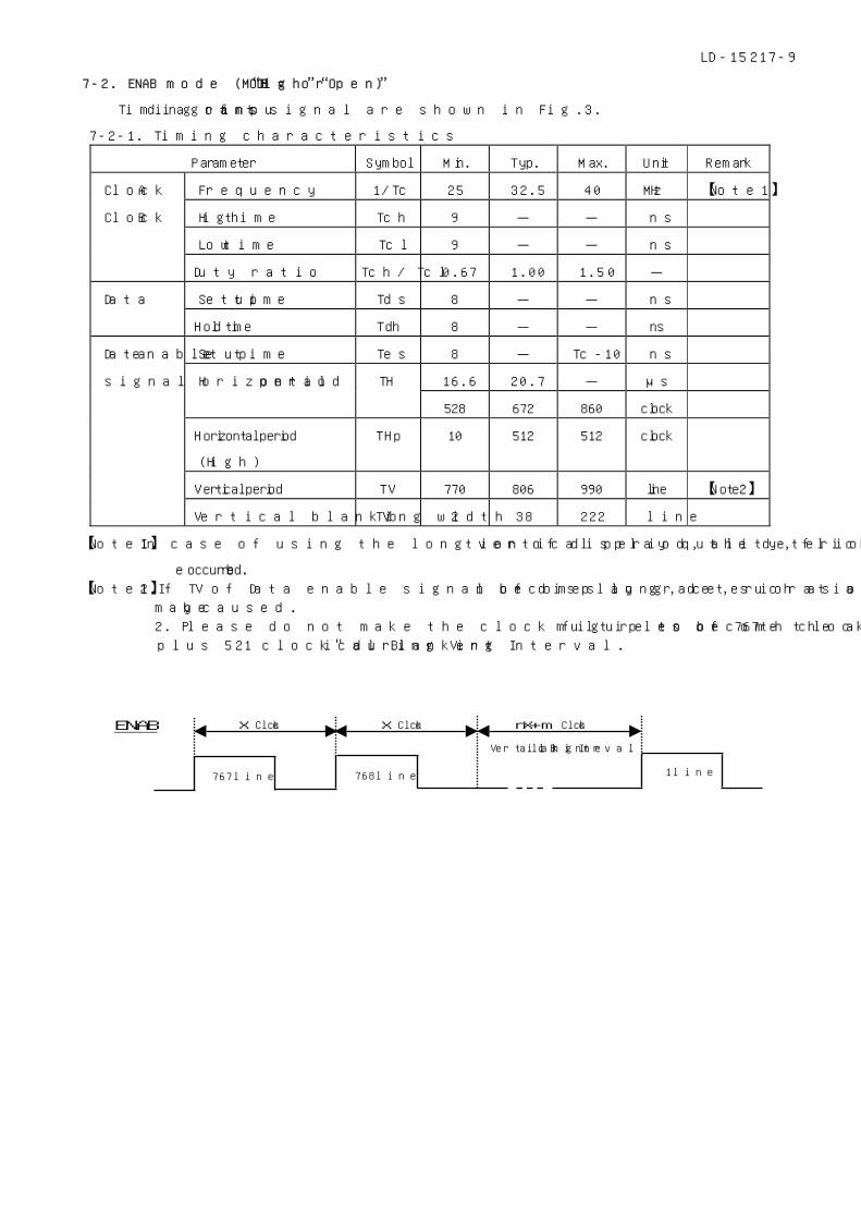
7-2. ENAB mode (MODE = “High” or “Open” )
Timing diagrams of input signal are shown in Fig.3.
7-2-1. Timing characteristics
Parameter Symbol Min. Typ. Max. Unit Remark
Clock A Frequency 1/Tc 25 32.5 40 MHz 【Note1】
Clock B High time Tch 9 - - ns
Low time Tcl 9 - - ns
Duty ratio Tch/ Tcl 0.67 1.00 1.50 -
Data Setup time Tds 8 - - ns
Hold time Tdh 8 - - ns
Data enable Setup time Tes 8 - Tc-10 ns
signal 16.6 20.7 - μs
Horizontal period TH
528 672 860 clock
Horizontal period
(High)
THp 10 512 512 clock
Vertical period TV 770 806 990 line 【Note2】
Vertical blanking width TVb 2 38 222 line
【Note1】 In case of using the long vertical period, the deterioration of display quality, flicker etc., may
be occurred.
【Note2】 1.If TV of Data enable signal becomes long, deterioration of display grace, such as a flicker,
may be caused.
2. Please do not make the clock figure to become the amount in "multiples of 767th clock line figure
plus 521 clock" during Vertical Blanking Interval.
ENAB
Vertical Blanking Interval
nX+m Clock X Clock X Clock
1line 768line 767line

LD-15217-10
7-3. Input Data Signals and Display Position on the screen
Graphics and texts can be displayed 1024 × 3× 768 dots on a panel with 262,144 colors by supplying 36 bit
data signal (6bit/color [64 gray scale] x 3 x 2 pixels) .
DA(1,1) DB(1,1) DA(2,1)
DA(1,2) DB(1,2)
DA(1,3)
DA(1,768)
DB(512,1)
R G B
DB(512,768)
RA GA BA RB GB BB
(1,1) (1,1) Two pixel-data are sampled at the same time.
*DA: RA0~RA5, GA0~GA5, BA0~BA5
*DB: RB0~RB5, GB0~GB5, BB0~BB5
Display position of input data(H,V)
7-4. Sleep Mode
This LCD module stops operation, and the picture of the LCD module becomes wholly white, if ENAB signal
stays "Low" for over 0.5 sec. Follow the above input signal timing for normal operation.
Over 0.5s
2.6V 0.6VENAB Signal

(1line) (2line)
DATA Signal A
RA0~RA5
GA0~GA5
BA0~BA5
Fig.3 Input Signal Waveforms(ENAB mode)
ENAB Signal
CLOCK Signal A
CLOCK Signal B
DATA Signal B
RB0~RB5
GB0~GB5
BB0~BB5
0.6V
TH
2.6V
Tes
THp
DATA Signal
RA0~RA5
GA0~GA5
BA0~BA5
RB0~RB5
GB0~GB5
BB0~BB5
DH767 DH768
Number of data
INVALID DH1 DH2 DH3
TV
INVALID
2.6V
DH1 DH2 DH3
2.6V
2.6V
ENAB Signal
Tds Tdh Number of data
INVALID
0.6V
DA1 DA2 DA3 DA511 DA5122.6V
INVALID DB2 DB3 DB511 DB5122.6V
Tch Tcl
2.6V
0.6V
0.6V
0.6V
INVALID
INVALID
Tc
TVb
0 .6V
DB1
LD
-1521
7-11
LD-15217-12
8. Input Signals, Basic Display Colors and Gray Scale of Each Color
Colors & Data signal
Gray scale Gray RA0 RA1 RA2 RA3 RA4 RA5 GA0 GA1 GA2 GA3 GA4 GA5 BA0 BA1 BA2 BA3 BA4 BA5
Scale RB0 RB1 RB2 RB3 RB4 RB5 GB0 GB1 GB2 GB3 GB4 GB5 BB0 BB1 BB2 BB3 BB4 BB5
Black - 0 0 0 0 0 0 0 0 0 0 0 0 0 0 0 0 0 0
Blue - 0 0 0 0 0 0 0 0 0 0 0 0 1 1 1 1 1 1
Green - 0 0 0 0 0 0 1 1 1 1 1 1 0 0 0 0 0 0
Cyan - 0 0 0 0 0 0 1 1 1 1 1 1 1 1 1 1 1 1
Red - 1 1 1 1 1 1 0 0 0 0 0 0 0 0 0 0 0 0
Magenta - 1 1 1 1 1 1 0 0 0 0 0 0 1 1 1 1 1 1
Yellow - 1 1 1 1 1 1 1 1 1 1 1 1 0 0 0 0 0 0
White - 1 1 1 1 1 1 1 1 1 1 1 1 1 1 1 1 1 1
Black GS0 0 0 0 0 0 0 0 0 0 0 0 0 0 0 0 0 0 0
GS1 1 0 0 0 0 0 0 0 0 0 0 0 0 0 0 0 0 0
Darker GS2 0 1 0 0 0 0 0 0 0 0 0 0 0 0 0 0 0 0
Brighter GS61 1 0 1 1 1 1 0 0 0 0 0 0 0 0 0 0 0 0
GS62 0 1 1 1 1 1 0 0 0 0 0 0 0 0 0 0 0 0
Red GS63 1 1 1 1 1 1 0 0 0 0 0 0 0 0 0 0 0 0
Black GS0 0 0 0 0 0 0 0 0 0 0 0 0 0 0 0 0 0 0
GS1 0 0 0 0 0 0 1 0 0 0 0 0 0 0 0 0 0 0
Darker GS2 0 0 0 0 0 0 0 1 0 0 0 0 0 0 0 0 0 0
Brighter GS61 0 0 0 0 0 0 1 0 1 1 1 1 0 0 0 0 0 0
GS62 0 0 0 0 0 0 0 1 1 1 1 1 0 0 0 0 0 0
Green GS63 0 0 0 0 0 0 1 1 1 1 1 1 0 0 0 0 0 0
Black GS0 0 0 0 0 0 0 0 0 0 0 0 0 0 0 0 0 0 0
GS1 0 0 0 0 0 0 0 0 0 0 0 0 1 0 0 0 0 0
Darker GS2 0 0 0 0 0 0 0 0 0 0 0 0 0 1 0 0 0 0
Brighter GS61 0 0 0 0 0 0 0 0 0 0 0 0 1 0 1 1 1 1
GS62 0 0 0 0 0 0 0 0 0 0 0 0 0 1 1 1 1 1
Blue GS63 0 0 0 0 0 0 0 0 0 0 0 0 1 1 1 1 1 1
Basic C
olor G
ray Scale of Red
Gray Scale of G
reen G
ray Scale of Blue
0 :Low level voltage, 1 : High level voltage
Each basic color can be displayed in 64 gray scales from 6 bit data signals. According to the combination of
total 18 bit data signals, the 262,144-color display can be achieved on the screen.
LD-15217-13
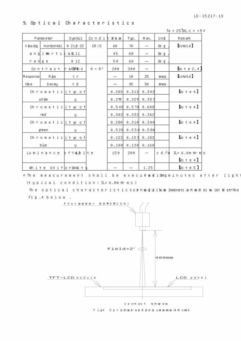
9. Optical Characteristics
Ta=25℃, Vcc=+5V
Parameter Symbol Condition Min. Typ. Max. Unit Remark
Viewing Horizontal θ21,θ22 CR>5 60 70 - Deg. 【Note1,4】
angle Vertical θ11 45 60 - Deg.
range θ12 50 60 - Deg.
Contrast ratio CRn θ=0° 200 300 - 【Note2,4】
Response Rise τr - 10 25 ms 【Note3,4】
time Decay τd - 35 50 ms
Chromaticity of x 0.283 0.313 0.343 【Note4】
white y 0.299 0.329 0.359
Chromaticity of x 0.548 0.578 0.608 【Note4】
red y 0.302 0.332 0.362
Chromaticity of x 0.280 0.310 0.340 【Note4】
green y 0.520 0.550 0.580
Chromaticity of x 0.123 0.153 0.183 【Note4】
blue y 0.100 0.130 0.160
Luminance of white YL1 150 200 - cd/m2 IL=6.0mArms
【Note4】
White Uniformity δW - - 1.25 【Note5】
※The measurement shall be executed 30 minutes after lighting at rating .
(typical condition:IL=6.0mArms)
The optical characteristics shall be measured in a dark room or equivalent state with the method shown in
Fig.4 below .
Photodetector (BM-5A:TOPCON)
Fig.4 Optical characteristics measurement method
Center of the screen
TFT-LCD module
400mm
Field=2°
LCD panel
LD-15217-14
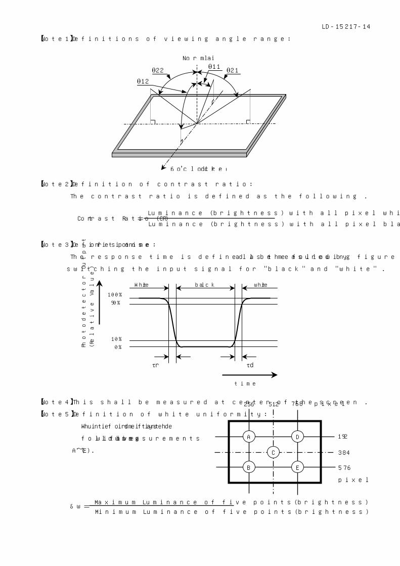
【Note1】Definitions of viewing angle range:
Norma line
6 o’clock direction
θ22
θ12
θ11 θ21
【Note2】Definition of contrast ratio:
The contrast ratio is defined as the following .
Luminance (brightness) with all pixel white
Luminance (brightness) with all pixel black Contrast Ratio (CR) =
【Note3】Definition of response time:
The response time is defined as the following figure and shall be measured by
switching the input signal for "black" and "white" .
White black white
100%
90%
10%
0%
τd τr
Photo
dete
cto
r O
utp
ut
(Rela
tive
Val
ue)
time
【Note4】This shall be measured at center of the screen . 256 512 768 pixel
E
D
B
C
A
【Note5】Definition of white uniformity:
White uniformity is defined as the
192 following with five measurements
(A~E) . 384
576
pixel
Maximum Luminance of five points(brightness)
Minimum Luminance of five points(brightness) δw=

LD-15217-15
10. Handling Precautions
a) Be sure to turn off the power supply when inserting or disconnecting the cable .
b) Be sure to design the cabinet so that the module can be installed without any extra stress such as warp
or twist .
c) Since the front polarize is easily damaged, pay attention not to scratch it .
d) Since long contact with water may cause discoloration or spots, wipe off water drop immediately .
e) When the panel surface is soiled, wipe it with absorbent cotton or other soft cloth. .
f) Since the panel is made of glass, it may break or crack if dropped or bumped on hard surface. Handle with
care .
g) Since CMOS LSI is used in this module, take care of static electricity and take the human earth into
consideration when handling .
h) Make sure the four mounting holes of the module are grounded sufficiently. Take electro-magnetic
interference (EMI) into consideration.
i) The module has some printed circuit boards (PCBs) on the back side. Take care to keep them form any
stress or pressure when handling or installing the module; otherwise some of electronic parts on the PCBs
may be damaged.
j) Observe all other precautionary requirements in handling components .
k) When some pressure is added onto the module from rear side constantly , it causes display non-uniformity
issue , functional defect , etc . So , please avoid such design .
l) When handling LCD modules and assembling them into cabinets, please be noted that long-term
storage in the environment of oxidization or deoxidization gas and the use of such materials as reagent,
solvent, adhesive, resin, etc. which generate these gasses, may cause corrosion and discoloration of the
LCD modules.
m) Duaring the module aging , don’t put protection film on the module surface.
11.Packing form
Form ① Form ②
Product country JAPAN TAIWAN
Piling number of cartons 5 cartons 5 cartons
Packing quantity in one carton 5 modules 5 modules
Carton size [mm] 410 (W)×500 (D)×255 (H) 420 (W)×500 (D)×270 (H)
Total mass of one carton filled
with full modules
8350 g 8700 g
Packing form is shown Fig .5 Fig .6

LD-15217-16
12.Reliability test items
No. Test item Conditions
1 High temperature storage test Ta=60℃ 240h
2 Low temperature storage test Ta=-25℃ 240h
3 High temperature
& high humidity operation test
Ta=40℃ ; 95%RH 240h
(No condensation)
4 High temperature operation test Ta=50℃ 240h
(The panel temp. must be less than 60℃)
5 Low temperature operation test Ta=0℃ 240H
6 Vibration test
(non- operating)
Frequency : 10~57Hz/Vibration width (one said) : 0.075mm
: 58~500Hz/Gravity : 9.8m/s2
Sweep time : 11minutes
Test period : 3 hours (1 hours for each direction X,Y,Z)
7 Shock test
(non- operating)
Max, gravity : 490m/s2
Pulse width : 11 ms, sine wave
Direction : ±X,±Y,±Z once for each direction
8 Thermal shock test
(operating)
Ta=-25℃~60℃ ; 5 cycles
Test period : 10 hours (1 hour for each temperature)
9 Altitude Ta=50℃,70kPa,3,048m(10,000ft), t=24h (Operating)
Ta=70℃,12kPa,15,240m(50,000ft), t=24h (Storage)
【Result Evaluation Criteria】
Under the display quality test conditions with normal operation state, these shall be no change
which may affect practical display function .
LD-15217-17
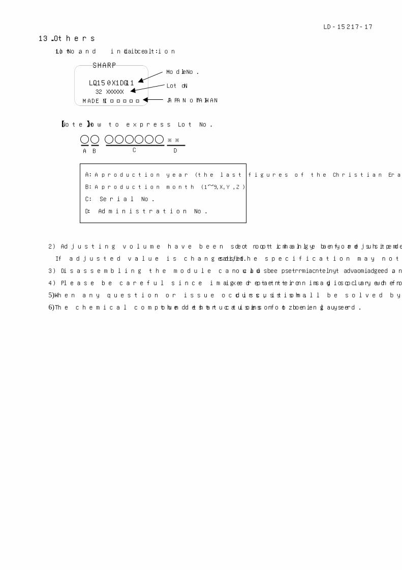
13.Others
1) Lot No. and indication Label:
SHARP
LQ150X1DG11 32 XXXXXX
MADE IN □□□□□
Model No.
Lot No.
JAPAN or TAIWAN
【Note】How to express Lot No.
C A B
※※ D
A: A production year (the last figures of the Christian Era)
B: A production month (1~9,X,Y,Z)
C: Serial No.
D: Administration No.
2) Adjusting volume have been set optimally before shipment, so do not change any adjusted value.
If adjusted value is changed, the specification may not be satisfied.
3) Disassembling the module can cause permanent damage and should be strictly avoided.
4) Please be careful since image retention may occur when a fixed pattern is displayed for a long time.
5) When any question or issue occurs, it shall be solved by mutual discussion.
6) The chemical compound that causes the destruction of ozone layer is not being used.

matsukawa.toshikazu
LD-15217-18

matsukawa.toshikazu
LD-15217-19

matsukawa.toshikazu
LD-15217-20