
Recent Developments of High Power Converters for Industry - Abb
15
Recent Developments of High Power Converters for Industry and Traction Applications S. Bernet Transactions on Power Electronics, November 2000, Foz do Iguaçu, Brazil Copyright © [2000] IEEE. Reprinted from the IEEE Transactions on Power Electronics. This material is posted here with permission of the IEEE. Such permission of the IEEE does not in any way imply IEEE endorsement of any of ABB Switzerland Ltd, Semiconductors's products or services. Internal or personal use of this material is permitted. However, permission to reprint/republish this material for advertising or promotional purposes or for creating new collective works for resale or redistribution must be obtained from the IEEE by writing to [email protected] .
Transcript of Recent Developments of High Power Converters for Industry - Abb

Recent Developments of High Power Converters for Industry and Traction Applications
S. Bernet
Transactions on Power Electronics, November 2000, Foz do Iguaçu, Brazil
Copyright © [2000] IEEE. Reprinted from the IEEE Transactions on Power Electronics.
This material is posted here with permission of the IEEE. Such permission of the IEEE does not in any way imply IEEE endorsement of any of ABB Switzerland Ltd, Semiconductors's products or services. Internal or personal use of this material is permitted. However, permission to reprint/republish this material for advertising or promotional purposes or for creating new collective works for resale or redistribution must be obtained from the IEEE by writing to [email protected].

ABB Corporate Research Recent Developments of High Power Converters
IEEE Transactions on Power Electronics page 1 of 14 Foz do Iguacu, Brazil November 2000
Recent Developments of High Power Convertersfor Industry and Traction Applications
S. BernetABB Corporate Research
P.O. Box 10133269003 Heidelberg
GermanyEmail: [email protected]
Abstract - The introduction of new high power devices likeIGCTs and high voltage IGBTs accelerates the broad use ofPWM voltage source converters in industrial and tractionapplications. This paper summarizes the state-of-the-art ofpower semiconductors. The characteristics of Integrated GateCommutated Thyristors (IGCTs) and high voltage IGBTs aredescribed in detail. Both the design and loss simulations of atwo level 1.14 MVA Voltage Source Inverter and a 6 MVAthree-level neutral point clamped Voltage Source Converterwith active front end enable a detailed comparison of bothpower semiconductors for high power PWM converters. Thedesign and the characteristics of a commercially availableIGCT neutral point clamped PWM voltage source converterfor medium voltage drives are discussed. Recent developmentsand trends of traction converters at dc mains and ac mains aresummarized.
I. INTRODUCTION
The development of new high power semiconductorssuch as 3.3kV, 4.5kV and 6.5kV Insulated Gate BipolarTransistors (IGBTs) and 4.5kV to 5.5kV Integrated GateCommutated Thyristors (IGCTs), improved converter de-signs and the broad introduction of three-level topologieshave led to a drastic increase of the market share of PWMcontrolled Voltage Source Converters (VSC). Meanwhilethese converters, ranging from 0.5 MVA to 10 MVA, arebecoming price competitive against conventional three-phase rectifiers and cycloconverters on the basis of thyris-tors since reduced line harmonics, a better power factor,substantially smaller filters and a higher system efficiencyenable a cost reduction of the system in many applicationslike for instance rolling mills, marine and mining applica-tions, electrolysis and high voltage DC transmission. De-spite a price reduction of Gate Turn Off thyristors (GTOs)by a factor of two to three over the last five years, alsoconventional GTO Voltage Source Converters and CurrentSource Converters (CSC) are increasingly replaced byPWM Voltage Source Converters with IGCTs or IGBTs intraction and industry applications.
Starting with a summary of the state of the art and trendsof power semiconductors, this paper compares IGCTs andhigh voltage IGBTs for high power applications, sincethere are almost no publications about this important sub-ject which determines fundamentally the design and theperformance as well as the investment and operating costsof high power converters for different applications. Spe-cific device characteristics are derived on the basis of adescription of the fundamental function and structure of
both high power switches. The design and simulation of a1.14 MVA two-level PWM Voltage Source Inverter (VSI)and a 6 MVA three-level voltage source converter withactive front end applying (3300V,1200A) IGBT modulesand 4.5kV IGCTs enable a detailed comparison andevaluation of both switches. The active silicon area, semi-conductor losses, the complexity of the gate drives, protec-tion, and reliability issues are addressed. Design issues andcharacteristics of a recently introduced PWM mediumvoltage converter family are discussed. A consideration ofrecent developments of traction converters at dc and acmains completes the paper.
II. RECENT DEVELOPMENT OF POWERSEMICONDUCTORS
A. State-of-the-Art and Trends
Fig. 1 and Fig. 2 summarize the most important powersemiconductors on the market and their rated voltages andcurrents today. Up to now silicon is clearly the dominatingsemiconductor material. According to the device structuressilicon semiconductors can be distinguished in diodes,transistors and thyristors. The diodes can be classified inSchottky diodes, epitaxial and double diffused pin diodes(Fig. 1). While Schottky diodes dominate at low voltages(Vbr 100V) and high switching frequencies, the fastswitching epitaxial (Vbr 600-1200V) and double diffusedpin diodes (Vbr 1000V) are applied at higher voltages.
MOSFETs and IGBTs have replaced Bipolar JunctionTransistors almost completely. Considering MOSFETs aremarkable development took place during the last twoyears. While the introduction of the so-called S-FET tech-nology in 1996 enables very low on-state resistances in thelow voltage range (Vbr<100V; e.g. RDSon<6m @VDS=30V), the development of the so called Cool-MOS in1998 enables a reduction of the on-state resistance RDSon bya factor of 5 to 10 compared to conventional verticalMOSFETs for the same chip area in a voltage range ofVbr=600V-1000V (Fig. 1). The introduction of vertical p-strips in the drift region and the resulting extension of thespace charge region also in horizontal direction allows adistinct reduction of the device thickness and thereforereduced on-state and switching losses and a lower gatedrive power of Cool-MOS. The area related maximumpermissible avalanche energy, ruggedness and reliability ofthe device are retained [2]. Nowadays MOSFETs are avail-
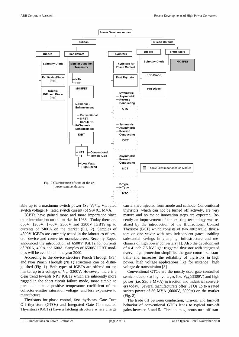
ABB Corporate Research Recent Developments of High Power Converters
IEEE Transactions on Power Electronics page 2 of 14 Foz do Iguacu, Brazil November 2000
able up to a maximum switch power (SS=VS*IS; VS: ratedswitch voltage; IS: rated switch current) of SS= 0.1 MVA.
IGBTs have gained more and more importance sincetheir introduction on the market in 1988. Today there are600V, 1200V, 1700V, 2500V and 3300V IGBTs up tocurrents of 2400A on the market (Fig. 2). Samples of4500V IGBTs are currently tested in the laboraties of sev-eral device and converter manufacturers. Recently Eupecannounced the introduction of 6500V IGBTs for currentsof 200A, 400A and 600A. Samples of 6500V IGBT mod-ules will be available in the year 2000.
According to the device structure Punch Through (PT)and Non Punch Through (NPT) structures can be distin-guished (Fig. 1). Both types of IGBTs are offered on themarket up to a voltage of Vbr=3300V. However, there is aclear trend towards NPT IGBTs which are inherently morerugged in the short circuit failure mode, more simple toparallel due to a positive temperature coefficient of thecollector-emitter saturation voltage and less expensive tomanufacture.
Thyristors for phase control, fast thyristors, Gate TurnOff thyristors (GTOs) and Integrated Gate CommutatedThyristors (IGCTs) have a latching structure where charge
carriers are injected from anode and cathode. Conventionalthyristors, which can not be turned off actively, are verymature and no major innovation steps are expected. Re-cently an improvement of the existing technology was re-alized by the introduction of the Bidirectional ControlThyristor (BCT) which consists of two antiparallel thyris-tors on one waver with two independent gates enablingsubstantial savings in clamping, infrastructure and me-chanics of high power converters [1]. Also the developmentof a 4 inch 7.5 kV light triggered thyristor with integratedovervoltage protection simplifies the gate control substan-tially and increases the reliability of thyristors in highpower, high voltage applications like for instance highvoltage dc transmission [3].
Conventional GTOs are the mostly used gate controlledsemiconductors at high voltages (i.e. VBR 3300V) and highpower (i.e. S 0.5 MVA) in traction and industrial convert-ers today. Several manufacturers offer GTOs up to a ratedswitch power of 36 MVA (6000V, 6000A) on the market(Fig. 2).
The trade off between conduction, turn-on, and turn-offbehavior of conventional GTOs leads to typical turn-offgains between 3 and 5. The inhomogeneous turn-off tran-
Today: Low Importance on Market
Schottky-Diode
Expitaxial-Diode(PIN)
DoubleDiffused Diode
(PIN)
Diodes
NPNPNP
Bipolar JunctionTransistor
ConventionalS-FETCool-MOS
N-Channel-Enhancement
P-Channel-Enhancement
MOSFET
NPT
Low VCEsat
High Speed
PTConventionalTrench-IGBT
IGBT
Transistiors
Thyristors forPhase Control
SymmetricAsymmetricReverseConducting
Fast Thyristor
SymmetricAsymmetricReverseConducting
GTO
AsymmetricReverseConducting
IGCT
P-TypeN-Type
MCT
MTO
Thyristors
Silicon
Schottky-Diode
JBS-Diode
PIN-Diode
Diodes
MOSFET
Transistors
Silicon Carbide
Power Semiconductors
Fig. 0 Classification of state-of-the-artpower semiconductors

ABB Corporate Research Recent Developments of High Power Converters
IEEE Transactions on Power Electronics page 3 of 14 Foz do Iguacu, Brazil November 2000
sient caused by the constriction of the turn-off current to-wards the center of the cathode islands limits the turn-offdv/dt to about 500-1000V/ s requiring bulky and expen-sive snubber circuits [1], [7]. The rather complex gatedrive as well as the relatively high power required to con-trol the GTO are other substantial disadvantages. How-ever, the high on-state current density, the high blockingvoltages, the high off-state dv/dt withstand capability, andthe possibility to integrate an inverse diode are consider-able advantages of these devices.
Substantial improvements of the conventional GTOstructure, the gate drive, the packaging, and the integratedinverse diode as well as the change of the turn-off processresulted in a drastically improved GTO which is consideredas a new component - the IGCT. 4.5kV (1.9kV/2.7kV dc-link) and 5.5kV (3.3kV dc-link) IGCTs with currents of275A Itgqm 4000A have been developed (Fig. 2). Theintroduction of a 6kV/6kA IGCT on the market was an-nounced for 1999. An extension of the blocking voltage ofIGCTs and inverse diodes to 10kV is technically possible.Thus the development of 10kV IGCTs depends basicallyon the market volume for these devices. Electroactivepassivation will substantially increase the maximum junc-tion temperatures of IGCTs in the near future [1].
Compared to GTOs both IGCTs and IGBTs have thepotential to decrease the costs and to increase the powerdensity as well as the performance of high power convert-ers because of snubberless operation at higher switchingfrequencies (e.g. fs=500-1000Hz).
Various new concepts of MOS controlled thyristors likee.g. the MOS Controlled Thyristor (MCT) and the MOSTurn Off Thyristor (MTO) have been proposed. However,at the moment the importance of these devices on the mar-ket is very low.
Marvelous physical properties of the material SiliconCarbide (SiC) like a wide energy gap (Si: 1.12eV; 4H-SiC:3.26eV), a high breakdown electric field (Si: 2.5*105V/cm;4H-SiC: 2.2*106V/cm for 1000V operation), a high thermalconductivity (Si: 1.5 W/cm; 4H-SiC: 4.9 W/cm at 25°C), ahigh saturated electron drift velocity (Si: 1.0*107cm/s; 4H-SiC: 2.0*107cm/s for E 2.0*105 V/cm), high inertness tochemical reaction and the high pressure and radiation re-sistance are the reason, that SiC will be a future material forpower semiconductors enabling a drastic reduction of on-state and switching losses and an operation at junction
102 103 104
104
103
102
200
1700
2500
3300
5500
7500
2400 4000 6000 I [A]
V [V]
Power MOSFET
IGBT (market)
IGCT (market)
SCR
6000GTO
200V/500A(Semikron)
200 500
5500V/2300A(ABB)
3300V/1200AModule (Eupec)
1700V/2400AModule (Eupec)
2500V/1800APress-Pack (Fuji)
4500V/4000A(Mitsubishi)
12000
12000V/1500A(Mitsubishi) 7500V/1650A
(Eupec)
6500V/2650A(ABB)
4800V/5000A(Westcode)
6000V/6000A GTO(Mitsubishi)
6500V/600A(Eupec IGBTannounced for 2000)
6000V/6000A IGCT(Mitsubishi IGCTannounced for 1999)
IGBT (announced)
Fig. 1 Power range of commercially available power semiconductors
temperatures up to Tj=600°C. SiC based Schottky andJunction Barrier Schottky (JBS) diodes have been built andtested for blocking voltages up to 2000V. Pin diodes havebeen realized up to 5kV. Due to extremely low reverserecovery currents even at high di/dt’s and high commuta-tion voltages, SiC diodes allow a drastic reduction of thediode turn-off losses and the turn-on losses of hard switch-ing IGBTs and MOSFETs. At the moment the defect den-sity of SiC wafers is the limiting factor for high powerdevices. However, it seems to be feasible to have proto-types of IGBT modules with SiC inverse diodes before theend of the year 1999 [1].
III. CHARACTERIZATION OF HIGH VOLTAGEIGBTS AND IGCTS
Both IGBTs and IGCTs have the potential to replaceGTOs since both switches allow substantial cost savingsdue to snubberless operation. To enable a comparison ofIGCTs and high voltage IGBTs (VCE 3300V) specificdevice characteristics are derived on the basis of a descrip-tion of the fundamental function and structure of a (3300V,1200A) IGBT module and reverse conducting 4.5kVIGCTs.
A. High Voltage IGBTs
1.) Package and Design: All high power IGBTs consistof many parallel chips due to the applied „MOS technol-ogy“. Today the maximum chip size of IGBTs is limited to4.6 cm2 [12].
There are basically two types of packages for 3.3kV,4.5kV and 6.5kV IGBTs - the module package and thepress pack.
In a module each chip is covered by a very thin (about5 m) aluminum metallization.

ABB Corporate Research Recent Developments of High Power Converters
IEEE Transactions on Power Electronics page 4 of 14 Foz do Iguacu, Brazil November 2000
Fig. 2 Physical arrangement of a (4500V, 1000A)-IGBT module
Fig. 3 Physical arrangement of an IGBT press pack
The connections of the IGBT and diode chips are real-ized by aluminum wires which are bonded to the chip met-allization by ultrasonic soldering [20]. As an example 450wires with 900 wedge bonds are required in a (3300V,1200A)-IGBT module. To protect the wire bond solderingthe plastic box of the module is filled with silicon gel. Arecently introduced special coating of bond wires is used toimprove the durability of bond wires in power cycling tests.The IGBT and the diode chips are soldered on a DirectCopper Bonding (DCB) substrate consisting of a ceramiclayer of AlN (which provides the internal insulation) andtwo copper layers (one at each side). The insulating sub-strate is softly soldered on a copper or AlSiC base plate.Fig. 3 shows the basic structure of a (4500V, 1000A) IGBTmodule as an example.
The main advantages of the module package are the fullinsulation of the base plate which enables a simple coolingand the low packaging costs. The poor power cycling capa-bility, the undefined failure mode after short circuits whichcan not be turned off (open or shorted terminals) and thepossible explosion of IGBT modules during the failuremode are important drawbacks.
To overcome these disadvantages press pack IGBTshave been developed recently by Fuji and Toshiba (Fig. 4).Only press contacts are used for the current and heat flowthrough the press pack device. The fact, that the press packbehaves as short circuit after IGBT and/or diode chips weredestroyed in the failure mode enables the use of theseswitches in applications with a redundant series connection
of (N+1) or (N+2) devices in stacks. With a redundant(N+1) or (N+2) design the converter can continue opera-tion if one device fails (is shorted). Since the replacementof the destroyed devices can be realized during plannedsystem services the availability of the converter is not af-fected by one or two device failures in a redundant design.The avoidance of explosions during the failure mode andthe possible increase of the reliability are other substantialadvantages of press packs. The distinctly increased costsand the required insulation of switch and cooling are disad-vantageous.
2.) On-state Behavior: High voltage IGBTs realize ac-ceptable current densities due to the bipolar injection ofcharge carriers. The conductivity modulation of IGBTscan be adjusted by the p-emitter efficiency and lifetimecontrol. The plasma distribution of up to date (3300V,1200A) IGBTs leads to substantially higher on-state lossescompared to latching devices. However, the introduction ofvertically optimized device structures has a substantialpotential to improve the plasma distribution and to decreasethe waver thickness enabling significantly reduced on-statevoltages and switching losses of future IGBTs.
3.) Switching Behavior: In Fig. 5 the snubberless turn-ontransient of a (3300V, 1200A) IGBT module in a VoltageSource Inverter at a dc-link voltage of Vdc=2250A and aload current of Io=1050A is depicted. The entire turn-ontransient takes about 1.2 s. Since hard turn-on transientsare basically determined by the turn-on transient of theIGBT internal MOSFET the occurring switching times, thedi/dt´s, and the dv/dt´s can be adjusted by the gate drive.The maximum rate of current rise diC/dt is limited by theSafe Operating Area (SOA) of the inverse diode whichdescribes the maximum peak reverse recovery current as afunction of the reverse blocking voltage of the diode [16].Therefore the minimum gate resistances for turn-on tran-sients depends essentially on the dc-link voltage and thestray inductances of the circuit.
Fig. 6 shows the measured snubberless turn-off transientof the (3300V, 1200A)-IGBT module. The small tail cur-rent is a typical characteristic of NPT-IGBTs. The gatedrive realizes a turn-off current fall of diC/dt=2800A/ s anda rate of voltage rise of dvCE/dt=3500V/ s. The turn-offtransient takes about 5 s. The occurring dvCE/dt as well asthe resulting turn-off losses can be adjusted in a wide rangeby the gate drive.
4.) Protection: The IGBT is able to limit its maximumcollector current which depends on the gate emitter voltageand the junction temperature. As an example for a (3300V,1200A)-IGBT module a gate voltage of 15V limits thecurrent to about three times the nominal current. If a shortcircuit appears the IGBT has to be turned off within 10 sfrom the active region.

ABB Corporate Research Recent Developments of High Power Converters
IEEE Transactions on Power Electronics page 5 of 14 Foz do Iguacu, Brazil November 2000
-2 0 2 4 6 8 10 12 14 s 18
2.5
2.0
1.5
1.0
0.5
0
2.0
kA
1.0
0
VCE[kV]
IC[kA]
Fig. 4 Measured hard turn-on transient of a (3300V, 1200A)-IGBT module (FZ1200R33KF1; Vdc=2.25kV; Io=1.05kA;Tj=25°C)
-2 0 2 4 6 8 10 12 14 s 18
1.2
0.8
0.4
0
3.0
2.0
1.0
0
IC[kA ]
V C E[kV ]
Fig. 5 Measured hard turn-off transient of a (3300V, 1200A)-IGBT module (Vdc=2.25kV; Io=1.05kA; Tj=25°C)
5.) Failure Mode: If a short circuit current can not beturned off, an IGBT module will be destroyed by the occur-ring large overcurrent caused by the fast discharge of thedc-link capacitor in a hard switching VSI. After the de-struction (explosion) the state of the module is not exactlydefined but most probably the module acts like two openterminals. In contrast an IGBT press pack acts as a shortcircuit in the failure mode.
6.) Gate Drive: Besides the recharge of the input ca-pacitance of the IGBT during turn-on and turn-off tran-sients the control of diC/dt and dvCE/dt during the switchingtransients, the supply under voltage protection, the adjust-ment of switching times and protection thresholds, as wellas the generation of error signals require sophisticated gatedrives with a substantial part count of analog and digitalelectronic devices.
7.) Reliability: In IGBT modules the thermo - mechani-cal stress of both wire bonds and solder between DCBsubstrate and base plate are critical issues. While the fa-tigue of the wire connections leads to a lift-off of wirebonds and thus to increased on state voltages, the degrada-tion of the internal thermal contacts caused by the thermo -mechanical stress of the solder between substrate and baseplate and the migration of the thermal contact grease leadto an inhomogeneous increased thermal resistance of themodule after thermal cycling. To increase the thermal cy-cling capability the copper base plate will be replaced by an
AlSiC base plate in IGBT modules. When using AlSiC asbase material the stresses of the solder interface are re-duced significantly due to a substantially reduced coeffi-cient of thermal expansion. In comparison to copper baseplates the use of AlSiC base plates in a (3300V, 1200A)Eupec IGBT module enables the increase of the thermalcycling capability from 3000 to 15000 cycles at TC=80Kand a reduction of the weight by about 30%. Furthermoreprotective bond coatings are increasingly applied in IGBTmodules to improve the thermal cycling capability of bondwires.
B. Integrated Gate Commutated Thyristors
1.) Package and Design: IGCTs are only offered in presspacks. The key idea of the IGCT is the hybridization of animproved GTO structure and an extremely low inductivegate drive. In contrast to high voltage IGBTs and its manyparts (e.g. 60 chips + 450 bond wires for a 3300V, 1200AIGBT module) Gate Commutated Thyristors (GCT) consistof only a few mechanical parts (Fig. 7):- the silicon waver which is divided in a GCT part and a
diode part for reverse conducting IGCTs- the gate ring which permits a low inductive contact from
the gate terminal to the gate segments on the waver- the molybdenum plates- the copper cases of anode and cathode- the gate ring terminal and- the gate unit with plate conductors having a total stray
inductance of 2-3 nH.
Fig. 8 shows one example of a GCT with integrated gatedrive (IGCT). The distance of 15 cm between gate driverand GCT guarantees that this arrangement will fit intodifferent types of stacks.
A substantial improvement of the GCT has beenachieved recently by the introduction of a buffer layer atthe anode side. Buffer layer power semiconductors gener-ate distinctly fewer on-state losses and switching lossesthan conventional NPT elements due to their up to 30%reduced device thickness for the same forward breakdownvoltage [9], [7]. In the new IGCTs the buffer layer is com-bined with a transparent anode which is basically a pn-junction with current dependent emitter efficiency. Triggercurrent and on-state gate current (or back porch current) arevery small since the emitter efficiency of the transparentanode is high at low current. On the other hand electronscan be extracted as efficiently as through conventionalanode shorts during turn-off because the transparent emitteris designed for low injection efficiency at high currentdensity in the latching state [9].In the past the advantages of monolithic NPT-GTO anddiode combinations were always diminished by the fact thatthe NPT-GTO required a thicker silicon chip than its corre-sponding free wheeling diode. Thus reverse conductingGTO devices suffered from excessive diode losses.

ABB Corporate Research Recent Developments of High Power Converters
IEEE Transactions on Power Electronics page 6 of 14 Foz do Iguacu, Brazil November 2000
Fig. 6 Mechanical parts of a Gate Commutated Thyristor (GCT)
Fig. 7 Physical arrangement of an Integrated Gate Commu-tated Thyristor
However, in the new buffer layer concept the minimumthickness of a PT-GCT and of the inverse diode are essen-tially the same which makes the monolithic GCT/inversediode configuration very attractive [9].
2.) On-state Behavior: Compared to currently available3.3kV and 4.5kV IGBTs, IGCTs have the important ad-vantage of substantially lower on-state voltages in the samevoltage class. Due to two injecting emitters GCTs enablehigh current densities (second only to thyristors) at low on-state voltages even at high blocking voltages due to thelatching state of the thyristor structure and a basically op-timum symmetric plasma distribution.
3.) Switching Behavior: The active turn-on transient ofthe IGCT at inductive loads is improved by the low induc-tance gate drive as well. The fast impression of the posi-tive gate current leads to a more homogenous turn-on tran-sient. In experiments no inhomogeneties have been ob-served at a rate of current rise of diA/dt 3000A/ s [8].However, to keep the turning off diode within its safe oper-ating area, the di/dt must be limited during the turn-ontransient of the IGCT. Due to the latching during the turn-on transient, the IGCT can not provide diA/dt (or dvAC/dt)control. Instead, a small concentrated turn-on snubberconsisting of an inductor, a free wheeling diode, a resistorand a clamp capacitor is necessary to limit the di/dt of theturning off diodes (Fig. 12). Additionally the di/dt clampcircuit relieves the turn-on transient of the IGCTs and
Fig. 8 Hard turn-off transient of a (4500V, 3000A)-IGCT(Vdc=3.5kV; Io=3kA; Tj=125°C, ts=1.6µs)
-1012345
05
1015202530
0 100 200 300 400 500 600 700
0
200
400
600
time [ s]
Fig. 9 25 kHz, 10-pulse test with a (5500V, 520A) IGCT 5SGX06F6004 (Vdc-link= 3.3kV, Tj (t = 0) = 80°C, Lr = 17µH, Load =2mH/50 m , ton = 10 s, toff = 30 s)
transfers losses to the clamp resistor which accepts highertemperatures and requires less cooling infrastructure thansemiconductors.
Fig. 9 shows the measured hard turn-off transient of a(4.5kV, 3kA) IGCT. Using a gate voltage of VGK=-20Vduring the turn-off transient, the negative gate current riseswith di dt kA sgn / /3 thereby commutating the com-plete cathode current to the gate before the main GTOblocking junction takes over voltage. Thus the GTOchanges from its pnpn latching state to the rugged transistorpnp mode within 1 s enlarging the SOA to full dynamicavalanche. Therefore the IGCT does not require any turn-off snubbers. If the load is purely inductive the anodecurrent remains unchanged until the IGCT voltage reachesthe dc-link voltage. The main part of the losses generatedduring the rise of the anode voltage is only determined bythe rate of voltage rise. As soon as the dc-link voltage isreached, the current commutates into the clamp. The oc-curring IGCT tail current is short due to the buffer layertechnology. The hard gate drive causes a storage time ofabout 1.6 s in the investigated operating point. In contrastto conventional GTOs, where a fairly long minimum timebetween consecutive turn-off transients is defined to returnto a uniform junction temperature, the homogenous turn-offtransient of IGCTs overcomes this drawback. Thereforeonly the thermal impedance limits the maximum switchingfrequency of IGCTs. As an example Fig. 10 presents a testpulse pattern where an IGCT is stressed with ten 25kHzpulses (10 s on, 30 s off).

ABB Corporate Research Recent Developments of High Power Converters
IEEE Transactions on Power Electronics page 7 of 14 Foz do Iguacu, Brazil November 2000
vo1
vo2
vo3
io1
io2
io3
VDC
S2 S4 S6
S1 S3 S5
Fig. 10 Circuit configuration of a two-level IGBT inverter
4.) Protection: The output short circuit protection profitsdirectly from the fast switching of IGCTs. If the di/dt of anexternal short circuit current is limited by a filter or a cableinductance the IGCTs can turn off before the maximumturn-off current of the semiconductors is reached [8].
In the case of an internal shoot through the di/dt clamp ofthe inverter limits the maximum peak current. Of courseprotection firing of all elements is possible in order to re-duce the stress of the defect phase. A shoot through willsafely discharge the dc-link since the IGCTs will safelyshort circuit under all worst-case failure conditions.
5.) Failure Mode: If an IGCT is destroyed, the presspack acts as a short circuit. This is especially advantageousin converters with series connected devices in a redundantdesign (e.g. (n+1)).
6.) Gate Drive: The IGCT gate drive delivers the re-quired gate current for the switching transients and the on-state. Despite the increase of the amplitude of the gatecurrent Igqrm the gate turn-off charge Qgq is reduced to about40% of that of a conventional GTO since the storagecharge is decreased by a factor of 1/15. This and the 90%reduction of the on-state gate current leads to a 50% reduc-tion of the gate drive power in comparison to a GTO. Therequired gate drive power of a (4500V, 1500A) IGCT isabout 5 times the gate drive power of the (3300V, 1200A)IGBT module in a 1.14 MVA PWM inverter operating at aswitching frequency of 500Hz. The fast switching tran-sients of the IGCTs do not require a control of the switch-ing times on the gate drive itself. It is interesting to notethat the part count of the IGCT gate drives is only slightlyhigher than that of a standard IGBT gate drive.
7.) Reliability: Due to a low total part count and proventechnology of GTO press packs a high reliability is guar-anteed. A number of qualification tests, field experience onreliability of key components (up to 400 million deviceoperations hours), and recent data from a 100 MVA rail-way inertie indicate a Failure in Time (FIT) of a full 3MVA inverter of FIT 2300 where 1 FIT= 1 Failure in onebillion hours. The contribution of the gate drivers is notsignificantly larger than with standard 600V-1200V IGBT
vo1
vo2
vo3
io1
io2
io3
DC
VDCCC
LC
S2 S4 S6
S1 S3 S5
RC
Fig. 11 Circuit configuration of a two-level IGCT inverter
inverters, since fiber optics and logic units are similar andthe power devices including the pulse capacitors behaveextremely well.
IV. COMPARISON OF HIGH VOLTAGE IGBTS ANDIGCTs IN HIGH POWER CONVERTERS
A. Two-Level PWM Voltage Source Inverter
To compare IGCTs and IGBTs in a two-level PWM-VSIthe lower part of the power range of IGCT converters waschosen. The considered inverter (Vdc=1500V, V1l=1100V,Io=600A, S=1.14 MVA) features sinusoidal modulationwith added third harmonics. The IGBT inverter was as-sumed to operate totally snubberless to achieve a minimumpart count (Fig. 11). In contrast to that a small di/dt clampwas assumed in the IGCT inverter to limit the rate of cur-rent rise to about diA/dt=800A/ s (Fig. 12).
The following devices were chosen: IGBT-Module:FZ1200R33KF1 (VCES=3300V, IC=1200A) [19], reverseconducting IGCTs: 5SGX08F4502 (VDRM=4500V, Vdc-
link=1900V, Itgqm=1560A) [11], and 5SGX26L4502(VDRM=4500V, Vdc-link=1900V, Itgqm=3120A) [11].
Both IGBT and IGCT can be operated up to a dc-linkvoltage of about Vdc=2200V. All devices have a propor-tion of about 2:1 between IGBT/IGCT and diode chip sizearea. It should be noted that the active area of the (4500V,3120A) IGCT is only 69% of the active area of the (3300V,1200A) IGBT. The active area of the integrated inversediode of the (4500V, 3120A) reverse conducting IGCT isonly about 58% of the active area of the inverse diode ofthe IGBT module. Considering the (4500V, 1560A) IGCTthe active area of this IGCT and the integrated inversediode are only 33% of the active area of the IGBT and theinverse diode respectively. To compare IGBT and IGCTinverters both inverters were simulated using a previouslydeveloped accurate power semiconductor loss model [25].
Fig. 13 shows the sum of conduction (Pcon_IGCT+D,Pcon_IGBT+D) and switching losses (Psw_IGCT+D, Psw_IGBT+D) ofthe considered IGBTs, IGCTs, and inverse diodes of thePWM inverter as a function of the modulation index
dc
pho
VV
m ,ˆ
232 (1)
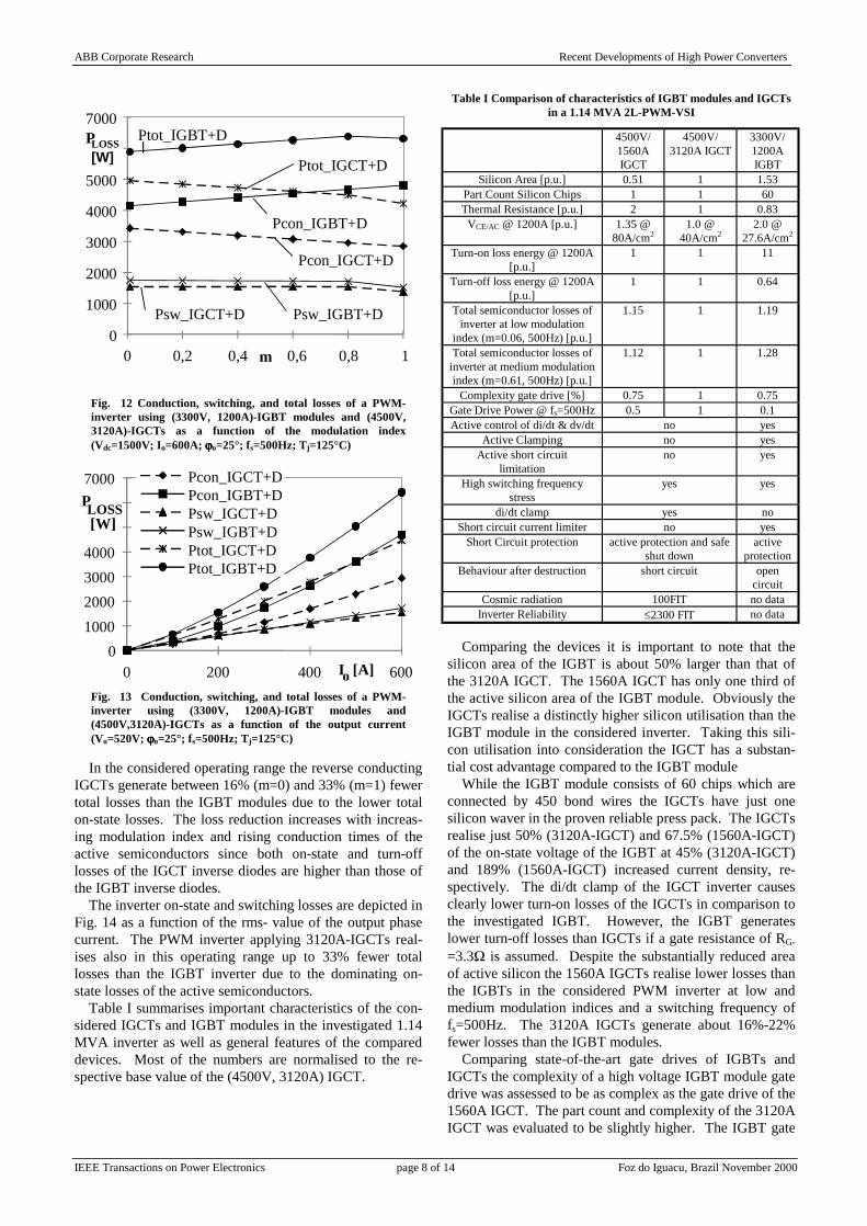
ABB Corporate Research Recent Developments of High Power Converters
IEEE Transactions on Power Electronics page 8 of 14 Foz do Iguacu, Brazil November 2000
0
1000
2000
3000
4000
5000
6000
7000
0 0,2 0,4 0,6 0,8 1m
PLOSS[W] Ptot_IGCT+D
Ptot_IGBT+D
Psw_IGCT+D Psw_IGBT+D
Pcon_IGBT+D
Pcon_IGCT+D
Fig. 12 Conduction, switching, and total losses of a PWM-inverter using (3300V, 1200A)-IGBT modules and (4500V,3120A)-IGCTs as a function of the modulation index(Vdc=1500V; Io=600A; o=25°; fs=500Hz; Tj=125°C)
01000200030004000
5000
60007000
0 200 400 600Io [A]
PLOSS[W]
Pcon_IGCT+DPcon_IGBT+DPsw_IGCT+DPsw_IGBT+DPtot_IGCT+DPtot_IGBT+D
Fig. 13 Conduction, switching, and total losses of a PWM-inverter using (3300V, 1200A)-IGBT modules and(4500V,3120A)-IGCTs as a function of the output current(Vo=520V; o=25°; fs=500Hz; Tj=125°C)
In the considered operating range the reverse conductingIGCTs generate between 16% (m=0) and 33% (m=1) fewertotal losses than the IGBT modules due to the lower totalon-state losses. The loss reduction increases with increas-ing modulation index and rising conduction times of theactive semiconductors since both on-state and turn-offlosses of the IGCT inverse diodes are higher than those ofthe IGBT inverse diodes.
The inverter on-state and switching losses are depicted inFig. 14 as a function of the rms- value of the output phasecurrent. The PWM inverter applying 3120A-IGCTs real-ises also in this operating range up to 33% fewer totallosses than the IGBT inverter due to the dominating on-state losses of the active semiconductors.
Table I summarises important characteristics of the con-sidered IGCTs and IGBT modules in the investigated 1.14MVA inverter as well as general features of the compareddevices. Most of the numbers are normalised to the re-spective base value of the (4500V, 3120A) IGCT.
Table I Comparison of characteristics of IGBT modules and IGCTsin a 1.14 MVA 2L-PWM-VSI
4500V/1560AIGCT
4500V/3120A IGCT
3300V/1200AIGBT
Silicon Area [p.u.] 0.51 1 1.53Part Count Silicon Chips 1 1 60Thermal Resistance [p.u.] 2 1 0.83
VCE/AC @ 1200A [p.u.] 1.35 @80A/cm2
1.0 @40A/cm2
2.0 @27.6A/cm2
Turn-on loss energy @ 1200A[p.u.]
1 1 11
Turn-off loss energy @ 1200A[p.u.]
1 1 0.64
Total semiconductor losses ofinverter at low modulation
index (m=0.06, 500Hz) [p.u.]
1.15 1 1.19
Total semiconductor losses ofinverter at medium modulationindex (m=0.61, 500Hz) [p.u.]
1.12 1 1.28
Complexity gate drive [%] 0.75 1 0.75Gate Drive Power @ fs=500Hz 0.5 1 0.1Active control of di/dt & dv/dt no yes
Active Clamping no yesActive short circuit
limitationno yes
High switching frequencystress
yes yes
di/dt clamp yes noShort circuit current limiter no yes
Short Circuit protection active protection and safeshut down
activeprotection
Behaviour after destruction short circuit opencircuit
Cosmic radiation 100FIT no dataInverter Reliability 2300 FIT no data
Comparing the devices it is important to note that thesilicon area of the IGBT is about 50% larger than that ofthe 3120A IGCT. The 1560A IGCT has only one third ofthe active silicon area of the IGBT module. Obviously theIGCTs realise a distinctly higher silicon utilisation than theIGBT module in the considered inverter. Taking this sili-con utilisation into consideration the IGCT has a substan-tial cost advantage compared to the IGBT module
While the IGBT module consists of 60 chips which areconnected by 450 bond wires the IGCTs have just onesilicon waver in the proven reliable press pack. The IGCTsrealise just 50% (3120A-IGCT) and 67.5% (1560A-IGCT)of the on-state voltage of the IGBT at 45% (3120A-IGCT)and 189% (1560A-IGCT) increased current density, re-spectively. The di/dt clamp of the IGCT inverter causesclearly lower turn-on losses of the IGCTs in comparison tothe investigated IGBT. However, the IGBT generateslower turn-off losses than IGCTs if a gate resistance of RG-
=3.3 is assumed. Despite the substantially reduced areaof active silicon the 1560A IGCTs realise lower losses thanthe IGBTs in the considered PWM inverter at low andmedium modulation indices and a switching frequency offs=500Hz. The 3120A IGCTs generate about 16%-22%fewer losses than the IGBT modules.
Comparing state-of-the-art gate drives of IGBTs andIGCTs the complexity of a high voltage IGBT module gatedrive was assessed to be as complex as the gate drive of the1560A IGCT. The part count and complexity of the 3120AIGCT was evaluated to be slightly higher. The IGBT gate

ABB Corporate Research Recent Developments of High Power Converters
IEEE Transactions on Power Electronics page 9 of 14 Foz do Iguacu, Brazil November 2000
drives require about 10%-20% of the IGCT gate drivepower due to the MOS control of the high voltage IGBT.However, the absolute value of the gate drive power is verysmall for all semiconductors. The possibility to adjustdi/dt´s and dv/dt´s during switching transients using thegate drive, the possibility of active clamping, and the limi-tation of short circuit currents by the device combined withthe possibility to turn off actively short circuit currentswithin 10 s are advantageous features of the high voltageIGBTs. IGCTs and IGBTs have no problems with highswitching frequency stress of worst case pulse patterns.
The risk of a shoot through is always present in a dc-voltage-link inverter. Of course this situation has to behandled safely. In the IGCT inverter the surge current islimited by the di/dt clamp. The IGCTs will safely shortcircuit under all worst case failure conditions and the con-trol will stop the operation of the inverter immediately inthis case. A special short circuit current limiter can limitthe destruction of IGBT modules caused by a shootthrough. However, the open circuit of an IGBT moduleafter destruction is a serious drawback of this device inseveral applications, like for instance in converters withseries connection. At the moment there are not sufficientdata about the reliability of high voltage IGBTs in indus-trial or traction converters available. Today there are ex-cessive date of field experience of IGCTs. Recent datafrom qualification tests on a 100MVA railway intertie inGermany indicate that a Failure in Time of FIT 2300 is tobe expected for a full 3MVA IGCT inverter. Today theproven outstanding reliability of IGCT inverters is anothersubstantial advantage of this technology.B. Three-Level PWM Voltage Source Inverter with ActiveFront End
To extend the comparison of IGCTs and IGBTs to athree-level PWM-Voltage Source Converter a 6 MVA unit(Vdc=4840V, V1l=3300V, Io=1050A, S=6 MVA) consistingof a neutral point clamped inverter and rectifier was cho-sen. Fig. 15 shows the principle circuit configuration whichreplaces conventional cycloconverters in hot and cold roll-ing mills. The active front end enables a four quadrantoperation of the drive. A low cost transformer and filterdesign becomes possible by the basically sinusoidal inputcurrents of the rectifier which are generated by optimisedpulse patterns. Fig. 16 shows the IGCT topology using91mm reverse conducting IGCTs 5SGX18L6004(VDRM=4500V, Vdc-link=2700V, Itgqm=2190A) [26]. Foursmall di/dt clamps (LR=3.4µH) were assumed to limit therate of current rise to about diA/dt=700A/ s and to enable asave shut down of the converter in the rare case of an inter-nal shoot through in the converter. In contrast the IGBTconverter operates without any passive clamp or snubbercircuit (Fig. 17). However, the series connection of twosingle switch IGBT modules per switch position is neces-sary in up to date commercially available 3.3kV and4.16kV medium voltage drives if 3.3kV IGBTs are applied.
It should be noted that the active area of the (4500V,2190A) IGCT is only 69% (GCT) and 58% (inverse diode)compared to the IGBT and the inverse diode of the aforementioned (3300V, 1200A) IGBT moduleFZ1200R33KF1. Taking the necessary series connection ofIGBT modules into consideration the 3.3kV IGCT con-verter uses only 34.5% (GCT) and 29% (inverse diode) ofthe active silicon area of IGBTs and diodes in the 3.3kVIGBT converter. To simulate the converter losses theminimum IGBT switching losses using a very small gateresistance of RG+=1.8 RG-=3.3 and an optimum voltagedistribution between the two series connected IGBT mod-ules were assumed. In real industrial converters the IGBTgate units are adjusted to generate di/dt’s and dv/dt’s ofabout 3kA/µs and 3kV/µs during switching transients re-spectively to avoid large overvoltages in the converter andat the terminals of the machine. Furthermore small delaytimes during switching transients of series connectedIGBTs will cause additional IGBT switching losses duringthe active clamping operation of the IGBTs in real convert-ers [22]. Considering real conditions the switching losses ofindustrial IGBT converters will be distinctly higher than thesimulated values.
Fig. 18 shows the converter losses as a function of thephase current. Although the switching losses represent thebest case for the IGBT module, the reverse conductingIGCTs and the IGCT-clamps generate about 25% fewerlosses than the IGBT modules in inverter and rectifier at6MVA (Iph=1150A). The reason for the substantial losssavings of the IGCT converter are the substantially smalleron-state losses of the IGCTs.
The loss distribution of the IGCT and IGBT converter isdepicted in Fig. 19 for a rms value of the phase current of Io=525A. Obviously the IGCT converter (inverter and recti-fier) generates only 39% of the on-state losses of the IGBTconverter. In contrast the IGBT switching losses are onlyabout 69% of the sum of switching and clamp losses of theIGCT converter. However, assuming real gate drive condi-tions the IGBT switching losses are estimated to be ap-proximately equal to the sum of switching and clamp lossesof the IGCTs. Assuming the lowest possible switchinglosses for the IGBT module the IGCT converter, whichuses only about 30% of the active silicon area of the IGBTconverter, still generates about 20% fewer total converterlosses than the IGBT converter. Summarizing one can say,that low losses at small active silicon area, fast switching, asmall part count, the reliable press pack in a compact me-chanical arrangement which can be easily assembled enablethe design of low cost, compact, reliable, highly efficient,and 100% explosion free IGCT converters. 300 kVA-10MVA IGCT converters can be achieved without series orparallel connection of devices or converters. The simpleand robust series connection of IGCTs will extend thepower range of IGCT converters up to several 100 MVAfor the power system market.

ABB Corporate Research Recent Developments of High Power Converters
IEEE Transactions on Power Electronics page 10 of 14 Foz do Iguacu, Brazil November 2000
3L-NPC-VSR 3L-NPC-VSI
SM
Inverter 3.3kVSynchronous
Machine
DC Voltage LinkRectifier
(Active Front End)Mains
TransformerMedium Voltage
Mains (e.g. 20kV)3.3kVMains
Fig. 14 Principle schematic of a PWM 3L-NPC-Voltage Source Converter with active front-end
Vdc/2
Vdc/2 CC1i
CC2i
LR2i
LR1i T11i T21i T31i
T32iT22iT12i
T13i T23i T33i
T34iT24iT14i
DC1i
DC2i
RS1i
RS2i
CC1r
CC2r
LR2r
LR1rT11r T21r T31r
T32rT22rT12r
T13r T23r T33r
T34rT24rT14r
Vm1 .. m3
DC1r
DC2r
RS1r
RS2r
RECTIFIER INVERTERDC VOLTAGE LINK
Vl1 .. l 3io1 ... io3
Fig. 15 Circuit configuration of a 6 MVA 3L-NPC Voltage Source Converter with (4500V, 2190A) reverse conducting IGCTs fora 3.3kV drive
Vdc/2
Vdc/2
T11i
Vm1 .. m3
T21i T31i
T14i T24i T34i
T23i T33iT13i
T12i T22i T32i
T13r T23r T33r
T14r T24r T34r
T11r T21r T31r
T12r T22r T32r
Vl1 .. l3
RECTIFIER INVERTERDC VOLTAGE LINK
io1 ... io3
Fig. 16 Circuit configuration of a 6 MVA 3L-NPC Voltage Source Converter with (3300V, 1200A) IGBTs for a 3.3kV drive

ABB Corporate Research Recent Developments of High Power Converters
IEEE Transactions on Power Electronics page 11 of 14 Foz do Iguacu, Brazil November 2000
0
20000
40000
60000
80000
100000
120000
140000
0 200 400 600 800 1000 1200Io [A]
PLOSS
[W]
Psw_IGBT
Pcon_IGBT
Psw_IGCT+Pclamp
Pcon_IGCT
Ptotal_IGBT
Ptotal_IGCT
Fig. 17 Losses of a (3300V, 1200A)-IGBT and (4500V, 2190A)-IGCT converter of a 3.3kV drive vs. load current (Vll=3008V;Vdc=4840V; cos o=1; cos i=-1; fs=840Hz; Tj=125°C)
0
10000
20000
30000
40000
50000
IGCT IGBT IGCT IGBT IGCT IGBT
PLOSS f
[W]
PconT PconD PonT
PoffT PoffD Pclamp
INVERTER RECTIFIER CONVERTER
=99,32%=99,37%=99,17%
=99,39%
=98,50%
=98,77%
Fig. 18 Loss distribution at 3MW for a (3300V, 1200A)-IGBTand a (4500V, 2190A) IGCT converter of a 3.3kV drive(Vll=3008V; Vdc=4840V; Io=525A; cos o=1; cos i=-1;fs=840Hz; Tj=125°C)
High voltage IGBTs offer interesting features like activecontrol of dv/dt and di/dt, active clamping, short circuitlimitation, and active protection. However, higher on-stateand total losses, a substantially smaller utilization of theactive silicon area and higher costs are substantial disad-vantages of up to date high voltage IGBTs. The undefinedfailure mode, the explosion during a short circuit in the dc-link which can not be turned off and reliability problemsunder thermal cycling are additional drawbacks of IGBTsin the module package which are usually applied in indus-trial converters.
IV. NEW MEDIUM VOLTAGE PWM INVERTER FORVARIABLE SPEED DRIVES IN INDUSTRY
APPLICATIONSThere is a large variety of topologies to feed variable
speed medium voltage induction or synchronous machines.The customer can choose between old fashioned thyristorCurrent Source Inverters (CSI), PWM-CSIs applying con-ventional GTOs, multi-level inverters on the basis of lowvoltage IGBTs and three-level VSIs with IGCTs, highvoltage IGBTs and GTOs. However, the introduction ofnew products by different manufacturers shows, that thereis a trend towards PWM controlled 3L-NPC-VSIs. Thehigh reliability, low losses, low costs and the wide range ofthe switch power of the IGCTs available on the marketmake the IGCT to an excellent choice for medium voltagedrives. Since IGCTs are technically and economically pref-erable to GTOs and currently available 3.3kV/4.5kV IGBT
modules, a recently introduced IGCT converter family formedium voltage drives is described below.
Fig. 20 shows the circuit configuration of the compact3L-NPC-VSI ACS1000 [5], [6]. A 12-pulse diode bridgerealizes a reliable, efficient and low cost rectification of theinput voltage for applications, which do not require a re-generation of electrical energy into the mains like pumps,fans and conveyor belts. Using a properly designed trans-former, the standard IEEE 519-1992 can be fulfilled if theshort circuit power of the feeding line is at least about 30times higher than the rated power of the drive. In weakermains a 24-pulse diode rectifier can be applied [5].
The PWM inverter is offered for 2.3kV, 3.3kV and4.16kV mains which corresponds to typical dc-link voltagesof 3.4kV, 4.9kV and 5.9kV. 38mm, 51mm, 68mm and91mm 4.5kV and 5.5kV IGCTs with integrated inversediodes and discrete NPC diodes are used as power semi-conductors. A small concentrated di/dt clamp in the upperand the lower half bridge limits the di/dt of the turning offdiodes and the short circuit current.
The IGCT 3L-NPC-VSI realizes distinctly lower totallosses than an IGBT inverter due to substantially smalleron-state voltages of the IGCTs. The IGCTs are operatedwith an average switching frequency of fs=500Hz whichcorresponds to an average output frequency of the inverterof fo=1000Hz [6].
Substantial disadvantages of variable speed drives whichare fed by inverters without output filter are the necessaryderating of standard motors caused by the extra losses ofthe harmonics, the high insulation stress due to steepdv/dt’s at the inverter output (up to 10kV/µs for IGCTs andIGBTs) and the increased audible noise due to a non-sinusoidal magnetic flux of the iron core. In the VSI of Fig.20 the LC output filter, which is tuned to a resonance fre-quency of about 360Hz, in combination with an integratedactive damping function of the drive control completelyavoids these drawbacks [6]. Fig. 21 shows measured wave-forms of the modulated line to line output voltage of theinverter and the smoothed line to line input voltage of themotor for a 2.3kV induction machine. The correspondingspectrum of the motor voltage shows a total harmonic dis-tortion of 1.7% which is well below the IEEE 519-1992limit of 5% [5].
The grounding of the star point of the LC filter and anoptional common mode choke decrease common modedistortions to very low levels even if long cables (e.g. 300mbetween transformer and rectifier) are used.
The protection of the converter is characterized by a fu-seless design. Two reverse conducting IGCTs betweenrectifier and dc-link capacitor separate the rectifier from thedc-link in the rare case of an inverter failure. The turn-offtransients of these protection switches are so fast, that theline and diode currents just rise by some percent due to theeffective total stray inductance of the input informer. In thecase of a very improbable diode short, the transformerprotection switch is fast enough to protect the rectifier frommechanical destruction [5]

ABB Corporate Research Recent Developments of High Power Converters
IEEE Transactions on Power Electronics page 12 of 14 Foz do Iguacu, Brazil November 2000
3
IsolationTransformer
Rectifier DC-Link
Inverter Filter Motor
NInd.Motor
di/dt-choke
Fig. 19 Circuit configuration of a 3L-NPC-VSI with 12 pulse rectifier and LC filter
spec_V
0
6
12
18
24
3010^-3
0.0 0.1 0.2 0.3 0.4 0.5 0.6 0.7 0.8 0.9 1.0
kHz
gr003: V_uv V_V3uv
-4.0
-3.5
-3.0
-2.5
-2.0
-1.5
-1.0
-0.5
0.0
0.5
1.0
1.5
2.0
2.5
3.0
3.5
4.0kV
42 44 46 48 50 52 54 56 58 60
ms
Fig. 20 Waveforms (line to line voltage of inverter; line to linevoltage of motor) and spectrum of motor voltage (10 units areequal to 1% of fundamental) of a 2.3kV drive [5]
To enable an accurate speed control and an excellent dy-namic behavior, the stator field oriented direct torque con-trol (DTC) has been applied. DTC is a well proven sophis-ticated control scheme which works in thousands of lowvoltage drives in a large variety of industrial applications.The static speed control error is only about 10% of themotors slip i.e. for a standard ac machine it is in the rangeof 0.1%. To enable a fast commissioning the control soft-ware starts an identification run to identify the motor pa-rameters before the first start of the motor.
V. NEW POWER CONVERTERS FOR TRACTIONAPPLICATIONS
Traction converters are fed by dc mains (e.g. 750V;1.5kV; 3kV) or single phase ac lines (e.g. 15kV; 25kV) inelectric trains or from synchronous generators in diesel-electric locomotives. Up to date traction drives apply VSIfed induction machines due to the outstanding performanceand the high reliability in the entire required power range.To decrease investment costs the next development stepswill concentrate on a simplification of both the appliedconverter circuits and mechanical constructions. Increasedefficiencies will enable lower operating costs. Furthermoreperformance improvements like faster accelerations andhigher speeds require the development of concepts withreduced weight. Both the state-of-the-art and trends oftraction converters are briefly summarized below.
A. Traction Converters at DC Mains
The feeding of traction converters by dc mains is com-plicated by the large variations of the dc voltages of –30%to +40%. The most efficient and simple solution for a trac-tion converter is a two-level VSI which is directly con-nected via an LC filter to the dc mains (Fig. 22). However,until recently this circuit could not be applied since therewere no fast switching semiconductors with a sufficientblocking voltage available on the market. Therefore differ-ent circuit configurations with series connected input chop-pers, which also enable an efficient operation of the three-phase VSI by the generation of a stabilized dc-link voltage,were applied. As an example Fig. 23 shows a circuit, whichwas conventionally applied at 3kV mains. 4.5kV GTOsoperating at dc-link voltages of 2.6-2.8kV mains were thestandard power semiconductors.
The additional costs, weight and losses of the inputchoppers of conventional solutions are substantial disad-vantages. Today 1700V IGBT modules which are available

ABB Corporate Research Recent Developments of High Power Converters
IEEE Transactions on Power Electronics page 13 of 14 Foz do Iguacu, Brazil November 2000
DC - 3kV
IM
LF
Cd
Fig. 21 Traction converter directly connected to the dc mainsDC - 3kV
IM
Ld
CF
Cd1
Cd2
Cd
LF
Fig. 22 Two stage traction converter for operation at dc mains
IGBT
GTO
100
50
%
009897969594 99
Tram
Metro
Locomotives
Year
Fig. 23 Application of semiconductors in traction converters byADtranz [23]
up to 2400A enable a direct operation of two-level VSIs at750V dc mains. The maximum power of about 1MW of aVSI applying 1700V/2400A IGBTs enables the use intrams and subways. Now the availability of 3.3kV IGBTmodules up to currents of 1200A allows the use of the di-rectly connected VSI at 1500V dc mains. For the 3kV dcmains with a maximum dc voltage of 4.3kV water cooledphase modules on the basis of 6.5kV Punch Through GTOsare currently used. The recently introduced 6.5kV IGBTswill replace these GTOs in the future. Simulations showed,that inverters with a nominal dc-link voltage of Vdc=3kVconsisting of two parallel (6500V, 600A) IGBT modulesper switch position enable an increase of the phase current(output current) by 25% in comparison to the use of twoseries connected (3300V, 1200A) IGBT modules perswitch position, which have about the same installed switchpower. Fig. 24 shows the application of IGBTs and GTOsin traction converters by ADtranz. Obviously IGBTs willreplace conventional GTOs in traction converters more andmore. However, also the use of IGCTs is under considera-tion by different traction converter manufacturers.
15kV 16 Hz2/3
1~
1~=
= =
3~IM
Fig. 24 Conventional structure of a traction converter at ac mains
4
3
Module 2
Module 1
Module 3
Module n
Module n+15
2
1
15kV 16 Hz2/3
Fig. 25 Medium frequency topology of a future traction con-verter at ac mains [23]
1) Mains side multi-level converter2) DC/DC Converter and medium frequency transformer3) Dc-voltage-link4) PWM VSI and induction machine5) Auxiliary Converters
B. Traction Converters at AC Mains
Fig. 25 shows the typical circuit configuration of a con-ventional traction drive at ac mains. A low frequency trans-former (e.g. 16 2/3 Hz or 50Hz) realizes the connection tothe single phase medium voltage mains (e.g. 15kV or25kV). Depending on the required power two to six parallelconnected four quadrant drives convert the power betweenthe secondary single phase windings of the transformer andthe dc-voltage-link. A two-level VSI generates the adjust-able voltage for the induction machine. 4.5kV GTOs are theconventionally applied semiconductors.
To save costs at increased efficiency the locomotive 12Xon the basis of 4.5kV IGBTs has been put into operation.The locomotive operates at 15kV/ 16 2/3 Hz and 25kV/50Hz mains respectively. Both four quadrant convertersand VSI are realized on the basis of a Modular Power Con-verter [18].

ABB Corporate Research Recent Developments of High Power Converters
IEEE Transactions on Power Electronics page 14 of 14 Foz do Iguacu, Brazil November 2000
A drastic reduction of the weight of the transformer atdistinctly increased efficiency can be achieved by the newconverter topology shown in Fig. 26 [23]. A multilevelconverter, consisting of n four quadrant converters enablesa high resulting switching frequency towards the mains. Nsoft switching dc/dc converters allow by the use of ex-tremely compact distributed medium frequency transform-ers a drastic reduction of the total transformer weight com-pared to a conventional low frequency line transformer.The dc/dc converters are all connected in parallel at thesecondary side of the medium frequency transformers tofeed one dc-voltage-link. The new converter concept willenable a weight reduction of 50% of the entire line-sideconverter system including transformer and filter [23]. Firsttest layers with prototypes on the basis of this new con-verter concept can be expected for the year 2003.
VI. CONCLUSIONS
The recent development of new high voltage semicon-ductors like IGCTs and high voltage IGBTs enables sub-stantial cost reductions and performance improvements ofPWM converters for industrial and traction applications.Both line or load commutated thyristor converters andconventional GTO converters with dc current link or dcvoltage link are increasingly replaced by two and three-level PWM-VSIs with IGCTs and IGBTs in different in-dustrial and traction applications. A detailed comparison ofIGCTs and IGBTs showed, that IGCTs are the maturedevices for industrial medium voltage drives today. Lowlosses at small active silicon area, fast switching, a smallpart count, the reliable press pack in a compact mechanicalarrangement which can be easily assembled enable thedesign of low cost compact, reliable, highly efficient, and100% explosion free IGCT converters. 300kVA-10MVAIGCT converter can be achieved without series or parallelconnection of devices or converters. In traction applicationsboth the replacement of GTOs by IGBTs and new converterconcepts will lead to higher converter efficiencies andlower costs.
REFERENCES
[1] A. Scharf, “State of the Art and Future Trends”, PCIM Europe, No.3, 1998, pp. 108-126.
[2] L. Lorenz, G. Deboy, M. März, J. Stengl, A. Bachofner, „DrasticReduction of On-Resistance with Cool MOS“, PCIM Europe, No.5, 1998, pp. 250-258.
[3] J.M. Peter, „Power Components: Which Evolution? Consequencesof the Power Converter Design“, Conf. Rec.AES, 1997, pp. 101-108.
[4] S. Bernet, R. Teichmann, A. Zuckerberger, P. Steimer, “Comparisonof High Power IGBTs and Hard Driven GTOs for High PowerInverters”, Conf. Rec. of IEEE-APEC, 1998, pp. 711-718.
[5] J.K. Steinke, M.K. Buschmann, “Robust and Reliable MediumVoltage PWM Inverter with Motor Friendly Output”, Conf. Rec.VII. Seminario de Electronica de Potencia, Chile, 1999.
[6] J.K. Steinke, R. Vuolle, H. Prenner, J. Järvinen, ”New VariableSpeed Drive with Proven Motor Friendly Performance for MediumVoltage Motors”, Conf. Rec. IEEE-IEMDC, 1999, pp. 235 -239.
[7] H.E. Grüning, B. degard, J. Rees, A. Weber, E. Carroll, S. Eicher,„High Power Hard Driven GTO Module for 4.5kV/3kA SnubberlessOperation“, Conf. Rec. PCIM, 1996, pp. 169-183.
[8] H.E. Grüning, B. degard, “High Performance Low Cost MVAInverters Realized with Integrated Gate Commutated Thyristors(IGCT)“, Conf. Rec. EPE, 1997, pp. 2060-2065.
[9] S. Lindner, S. Klaka, M. Frecker, E. Caroll, H. Zeller, „A NewRange of Reverse Conducting Gate Commutated Thyristors forHigh Voltage, Medium Power Application“, Conf. Rec. EPE, 1997,pp. 1117-1124.
[10] P.K. Steimer, H.E. Grüning, J. Werninger, E. Carroll, S. Klaka, S.Lindner, „IGCT - A New Emerging Technology for High Power,Low Cost Inverters“, Conf. Rec. IAS, 1997, pp. 1592-1599.
[11] Data Sheet the of reverse conducting IGCTs 5SGX26L4502,5SGX08F4502, ABB Semiconductors, 1998.
[12] Y. Takahashi, T. Koga, K. Yoshikawa, K. Yamazaki, H. Kirihata,Y. Seki, F. Eschrich, „2.5kV/1.8kA Power Pack IGBT“, Conf. Rec.ETG Report 72, 1998, pp. 43-54.
[13] K. Sommer, J. Göttert, G. Lefranc, R. Spanke, „Multichip HighPower IGBT-Modules for Traction and Industrial Application“,Conf. Rec. EPE, 1997, pp. 1112-1116.
[14] H. Brunner, M. Hierholzer, T. Laska, A. Porst, R. Spanke, „3300VIGBT Module for Traction Application“, Conf. Rec. EPE, 1997, pp.1056-1059.
[15] H. Brunner, M. Bruckmann, M. Hierholzer, T. Laska, A. Porst,„Improved 3.5kV IGBT-Diode Chipset and 800A Module Applica-tions“, Conf. Rec. of IEEE-PESC, 1996, pp. 1748-1753.
[16] M. Hierholzer, R. Bayerer, A. Porst, H. Brunner, „Improved Char-acteristic of 3.3kV IGBT Modules“, Conf. Rec. PCIM, 1997, pp.201-204.
[17] K. Ishii, Y. Konishi, M. Takeda, E. Thal, G. Debled, „A New HighPower, High Voltage IGBT“, Conf. Rec. PCIM, 1997, pp. 185-190.
[18] G. Hilpert, T. Züllig, „Integrated Power Module in IGBT Technol-ogy for Modular Power Traction Converters“, Conf. Rec. EPE 1997,pp. 1106-1111.
[19] Technical Information IGBT Module FZ1200R33KF1, EUPEC,1998.
[20] A. Hamidi, G. Coquery, R. Lallemand, „Reliability of High PowerIGBT Modules Testing on Thermal Fatigue Effects due to TractionCycles“, Conf. Rec. EPE, 1997, pp. 3118-3122.
[21] R. Marquardt, M. Bakran, R. Sommer, J. Teigelkötter, „Applicationof High Voltage IGBT and GTO in Traction Converters“, Conf.Rec. ETG Report 72, 1998, pp. 273-286.
[22] M. Bruckmann, R. Sommer, M. Fasching, J. Sigg, „Application ofIGBTs in High Power Converters“, Conf. Rec. ETG Report 72,1998, pp. 221-234.
[23] G. Kratz, H. Strasser, „Drive Concepts for Future Railway Vehi-cles“, Elektrische Bahnen, 1998, pp. 333-337.
[24] R.W. De Doncker, „Recent Developments of Power ElectronicComponents for High Power Applications“, Conf. Rec. of the Con-ference: Modern Power Semiconductors and Power ElectronicSystems in Railway Applications, 1999, pp. 1-32.
[25] S. Bernet, T. Matsuo and T.A. Lipo, „A Matrix Converter UsingReverse Blocking NPT-IGBTs and Optimized Pulse Patterns“, Conf.Rec. IEEE-PESC, 1996, pp. 107-113.
[26] Data Sheet – Reverse Conducting IGCTs, ABB Semiconductors,Lenzburg, Switzerland, 1999.
[27] M.K. Buschmann, J.K. Steinke, “Robust and Reliable MediumVoltage PWM Inverter with Motor Friendly Output”, Conf. Rec.EPE, 1997, pp. 3502-3507.
[28] Th. Schütze, H. Berg, M. Hierholzer, “Further Improvements ofReliability of IGBT Modules”, Conf. Rec. IEEE-IAS, 1998, pp.1022-1025.


