Real Time Video Processing in FPGA
7
INNOPT -2012 1 Abstract—The Digital Signal Processing algorithms, which remained in paper till 1980s due to the high computational power required found widespread applications with the emergence of Digital Signal Processors (DSP). DSP with their special hardware for mathematically intensive tasks, provided engineers the first platform for the real-time implementations of such algorithms. However, soon the sequential nature of program execution in DSPs emerged as the bottleneck, especially for high performance systems. Industry’s solution to the problem was FPGA (Field Programmable Gate Array). FPGAs, with their flexible hardware dedicated DSP blocks and unmatched parallelism, provided novel ways for engineers to meet the ever increasing power requirements. NeST’s contribution towards this field was triggered by a customer requirement to develop an FPGA based Real-time Video Processing system to replace an existing ASIC based Video Processing System. The initial thinking to purchase independent IP cores and integrate them into a system didn’t work because of the exorbitant price of the IP cores. The only remaining solution was to develop our own IP cores to build the system. This paper details the specifications, architecture and performance of Video Scaler, Sharpness Enhancer and Picture Quality Enhancer IP cores thus developed. These models were developed as reusable IP cores, supported by Product Briefs, Datasheets and User Manuals, thereby forming a saleable Video Processing Suite. A comprehensive PC driven test platform was also implemented in the FPGA board to test the various video processing modules developed. The test platform can also be easily modified to test other video processing IP cores being developed like Edge Enhancer and H.264 Decoder. This experience is a stepping stone for NeST into high performance real-time signal processing in FPGA and provides the ideal base for our organization to penetrate into this high- tech area comprising of machine vision, industrial inspection, surveillance and security, biomedical imaging etc. Index Terms — Scaler, Sharpness, Gamma and Picture Quality I. INTRODUCTION he rise in complexity and need for more flexibility has brought in the need for new architectures capable of implementing algorithms in video and image processing. The conventional methods that were used for implementing these algorithms include use of Digital Signal Processor (DSP) or Application Specific Integrated Circuit (ASIC) based solutions. The DSP’s lacked the flexibility in implementation whereas ASIC based solutions proved to be too expensive. The ability of FPGA to implement highly parallel architecture proved to be a better alternative. It not only provided an alternate platform with high performance and flexibility, but also provided an added advantage of reduced time to market. For implementation of continuously improving algorithms, the flexibility of FPGA was found to be highly beneficial. The Multimedia and Video Imaging (MVI) domain is evolving into a high growth market, characterized by continuously changing standards, market and customer demands. This necessitates the need for solutions capable of providing flexibility and reducing time to market. Development of re-usable modules is one such solution. Considering this high potential, NeST has developed re- usable modules such as the Video Scaler, Sharpness Enhancer, Gamma Correction and Picture Quality Enhancer, each saleable as independent Video IP cores. Besides them, some other IP cores like the H.264 Decoder & Edge Enhancer are also under development. II. RE-USABLE VIDEO IP CORES The reusable IP cores developed includes Video Scaler, Sharpness Enhancer, Gamma Correction and Picture Quality Enhancer. The Picture Quality Enhancer Core consists of the following sub-cores namely Brightness, Contrast and Color Enhancer. The features common to all of the re-usable cores are:- 1. Support for RGB 8:8:8 color format 2. Support for input resolutions from QVGA to SXGA 3. Support for real-time video processing Most of these cores make use of the DSP structures available in Virtex-5 FPGA called DSP48E Slice, for achieving high performance. These slices are capable of being configured either as a multiplier or multiplier followed by an adder or subtracter. There are a total of 288 DSP slices available in the chosen Virtex-5 FPGA, making it an ideal platform for development and testing of complex signal processing algorithms. These DSP slices are provided with dedicated high speed routing and built-in pipeline stages to facilitate high-speed of operation. A. Video Scaler Scaling is a functionality commonly required in video processing system where zoom in/zoom out is used. It can Real Time Video Processing in FPGA George Philip, Harilal V R, Linu Mary Varghese, Priya Ranjini N, Soumya Jose T
-
Upload
quest-global-erstwhile-nest-software -
Category
Engineering
-
view
140 -
download
7
description
Reusable Video IP Cores give software engineering service providers flexibility and less time to market while catering to the ever increasing demands of customers. Read on to know more about the Reusable IP Cores developed by NeST Software.
Transcript of Real Time Video Processing in FPGA

INNOPT -2012 1
Abstract—The Digital Signal Processing algorithms, which
remained in paper till 1980s due to the high computational
power required found widespread applications with the
emergence of Digital Signal Processors (DSP). DSP with their
special hardware for mathematically intensive tasks, provided
engineers the first platform for the real-time implementations of
such algorithms. However, soon the sequential nature of
program execution in DSPs emerged as the bottleneck,
especially for high performance systems. Industry’s solution to
the problem was FPGA (Field Programmable Gate Array).
FPGAs, with their flexible hardware dedicated DSP blocks and
unmatched parallelism, provided novel ways for engineers to
meet the ever increasing power requirements.
NeST’s contribution towards this field was triggered by a
customer requirement to develop an FPGA based Real-time
Video Processing system to replace an existing ASIC based
Video Processing System. The initial thinking to purchase
independent IP cores and integrate them into a system didn’t
work because of the exorbitant price of the IP cores. The only
remaining solution was to develop our own IP cores to build the
system.
This paper details the specifications, architecture and
performance of Video Scaler, Sharpness Enhancer and Picture
Quality Enhancer IP cores thus developed. These models were
developed as reusable IP cores, supported by Product Briefs,
Datasheets and User Manuals, thereby forming a saleable Video
Processing Suite. A comprehensive PC driven test platform was
also implemented in the FPGA board to test the various video
processing modules developed. The test platform can also be
easily modified to test other video processing IP cores being
developed like Edge Enhancer and H.264 Decoder.
This experience is a stepping stone for NeST into high
performance real-time signal processing in FPGA and provides
the ideal base for our organization to penetrate into this high-
tech area comprising of machine vision, industrial inspection,
surveillance and security, biomedical imaging etc.
Index Terms — Scaler, Sharpness, Gamma and Picture
Quality
I. INTRODUCTION
he rise in complexity and need for more flexibility has
brought in the need for new architectures capable of
implementing algorithms in video and image processing. The
conventional methods that were used for implementing these
algorithms include use of Digital Signal Processor (DSP) or
Application Specific Integrated Circuit (ASIC) based
solutions. The DSP’s lacked the flexibility in implementation
whereas ASIC based solutions proved to be too expensive.
The ability of FPGA to implement highly parallel architecture
proved to be a better alternative. It not only provided an
alternate platform with high performance and flexibility, but
also provided an added advantage of reduced time to market.
For implementation of continuously improving algorithms,
the flexibility of FPGA was found to be highly beneficial.
The Multimedia and Video Imaging (MVI) domain is
evolving into a high growth market, characterized by
continuously changing standards, market and customer
demands. This necessitates the need for solutions capable of
providing flexibility and reducing time to market.
Development of re-usable modules is one such solution.
Considering this high potential, NeST has developed re-
usable modules such as the Video Scaler, Sharpness
Enhancer, Gamma Correction and Picture Quality Enhancer,
each saleable as independent Video IP cores. Besides them,
some other IP cores like the H.264 Decoder & Edge Enhancer
are also under development.
II. RE-USABLE VIDEO IP CORES
The reusable IP cores developed includes Video Scaler,
Sharpness Enhancer, Gamma Correction and Picture Quality
Enhancer. The Picture Quality Enhancer Core consists of the
following sub-cores namely Brightness, Contrast and Color
Enhancer.
The features common to all of the re-usable cores are:-
1. Support for RGB 8:8:8 color format
2. Support for input resolutions from QVGA to SXGA
3. Support for real-time video processing
Most of these cores make use of the DSP structures available
in Virtex-5 FPGA called DSP48E Slice, for achieving high
performance. These slices are capable of being configured
either as a multiplier or multiplier followed by an adder or
subtracter. There are a total of 288 DSP slices available in
the chosen Virtex-5 FPGA, making it an ideal platform for
development and testing of complex signal processing
algorithms. These DSP slices are provided with dedicated
high speed routing and built-in pipeline stages to facilitate
high-speed of operation.
A. Video Scaler
Scaling is a functionality commonly required in video
processing system where zoom in/zoom out is used. It can
Real Time Video Processing in FPGA
George Philip, Harilal V R, Linu Mary Varghese, Priya Ranjini N, Soumya Jose
T

INNOPT -2012 2
also change the incoming input video to any aspect ratio.
A typical application of this resolution conversion would be
the conversion of a VGA signal from a standard laptop output
to SXGA signal for display in LCD monitor.
The scaling functions are being used in a wide range of
applications which includes:-
1. Post processing of video signals from digital camera
2. Medical imaging applications
3. Home media solutions
4. Video Surveillance
5. Consumer Displays
The above lists of application are indicative of the range of
areas where scaler module is being used. Considering the
complexity of the algorithm used the availability of scaler
core as a re-usable core definitely provides an added
advantage for NeST over other vendors in the MVI market.
Features
The main features provided by this core includes:-
1. Provision for independent control on horizontal and
vertical scaling factors.
2. Minimum selectable area for scaling is (1 x 1) and
maximum is (1280 x 1024)
3. Minimum supported output area is (1 x 1) and the
maximum is (1280 x 1024).
4. The number of taps supported is 2.
5. The number of phases supported is 8.
Algorithm Used
The general 2D scaling factor equation can be represented as
shown:-
In the above equation, outpix(x, y) represents the output
pixels generated. inpix(x, y) is the input pixels contributing in
the scaler operation. Htap and Vtap are the number of
horizontal and vertical taps in the filter. The coefficients,
coeff (i, j), in this equation represents weightings applied to
the set of input samples chosen to contribute to one input
pixel, according to the scaling ratio.
Video scaling is the process of generating pixels that do not
exist in the original image. For computing output pixels from
a set of input pixels, we need to first predict the location of
the output pixels relative to the closest input image. Using the
above information it is possible to estimate the output by
using a filter with coefficients weighted accordingly.
The algorithm implemented in this module for scaling up is
the Bilinear Interpolation Algorithm and for scaling down is
the Nearest Neighbor Algorithm. Coefficient values are
adjusted so as to implement both the algorithms using the
same interpolation filter used in the core.
Fig 1: Possible output pixel positions during zoom in
operations
The two tap bilinear interpolation filter considers the two
adjacent pixels for generation of the output pixels. In the
above figure we can find that the space between the adjacent
input pixels are divided into 8 positions called phases so that
the output pixels falls into any one of these positions. The
filter considers the weighted average of all the four pixels to
arrive at its final interpolated value.
Fig 2: Conversion of (5 x 5) image to a (3 x 3) using the
nearest neighbor algorithm
The downscaling is achieved by using the nearest neighbor
algorithm. In this algorithm, the output pixel is assigned the
value of the nearest pixel in the input line and output line is
assigned the nearest line in the input frame.
Architecture
The scaler module contains the following logic blocks.
a. Scaling filter
b. Coefficient memory
INNOPT -2012 3
c. Pre-processing Line buffers
d. Controller
Fig 3: Block Diagram of the Video Scaler
The incoming input video is validated on the rising edge of
the input pixel clock and valid data input signal. The valid
video data gets stored in the line buffer for further processing.
The function of the coefficient memory is to store the scaling
filter coefficients. The controller module decides the opening
and closing of the processing window. It is also responsible
for providing the scaler parameters and filter parameters. The
scaling filter performs the scaling function at the sysclk rate
based on the data provided by the controller module from the
line buffer and the coefficient memory. The scaling filter
starts processing only if all the necessary input arrives at its
input and the post processing block is ready to accept a
processed line.
B. Sharpness
The sharpness module is a block used for enhancing the
sharpness of the incoming video.
The dependency of a large number of factors necessitates the
need for providing a user control for enhancing sharpness of
an image. There is a need for this module in various display
devices. This necessitates the advantage of a stand-alone and
re-usable core capable of easy integration with other cores in
a video processing system.
Features
The main features of this module are:-
1. Programmable sharpness levels of 16, 32 and 64
2. Support for direct video streaming input
3. Delay match support for input sync signals
Sharpness is used to describe the clarity of detail of a
particular image. It involves sharpening the edges of an
image. A generic edge enhancement method uses a high pass
filter to filter out edge information and this is added with the
original image to get the sharpness enhanced output.
Algorithm Used
The sharpness adjustment is performed by this module by
convolving the input image with kernel. The convolution
result is multiplied with the sharpness level. The result is
subtracted from the original pixel value and the subtracted
result will replace the original pixel value to obtain the
sharpness enhanced pixel.
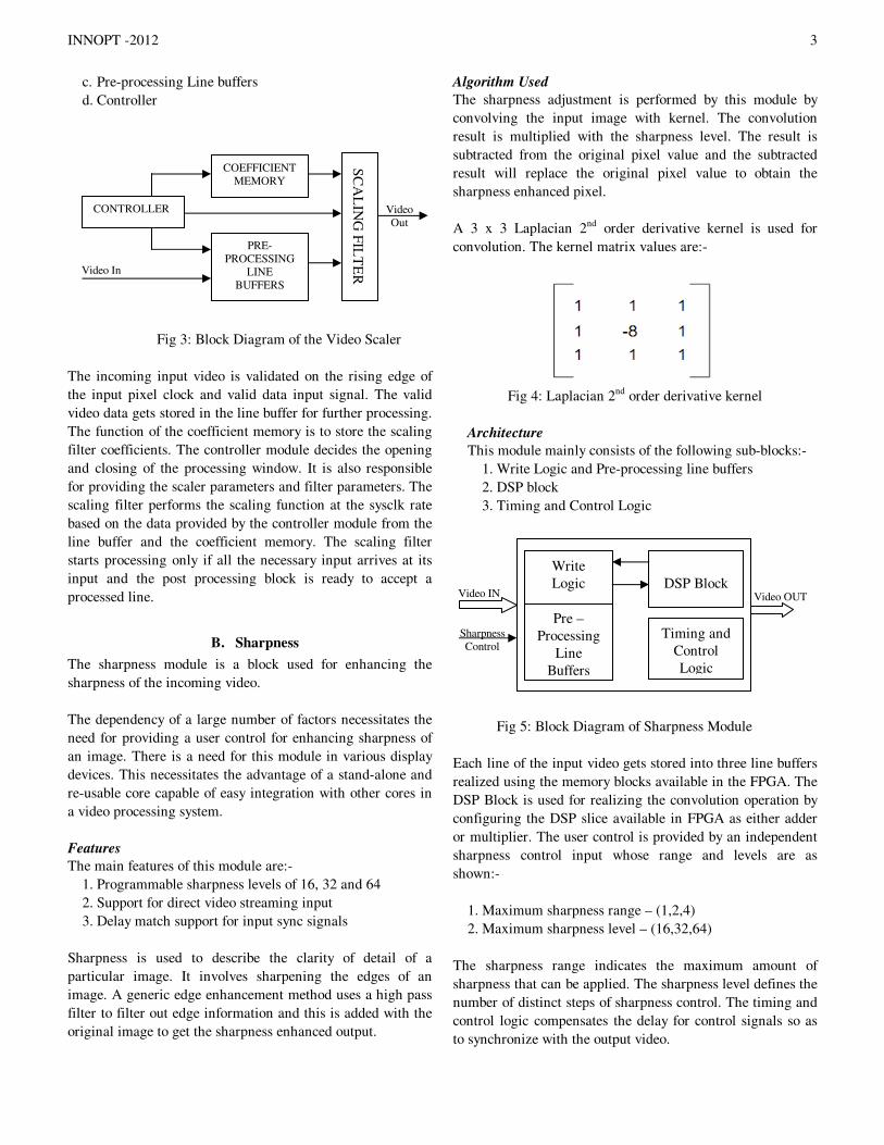
A 3 x 3 Laplacian 2nd order derivative kernel is used for
convolution. The kernel matrix values are:-
Fig 4: Laplacian 2nd order derivative kernel
Architecture
This module mainly consists of the following sub-blocks:-
1. Write Logic and Pre-processing line buffers
2. DSP block
3. Timing and Control Logic
Fig 5: Block Diagram of Sharpness Module
Each line of the input video gets stored into three line buffers
realized using the memory blocks available in the FPGA. The
DSP Block is used for realizing the convolution operation by
configuring the DSP slice available in FPGA as either adder
or multiplier. The user control is provided by an independent
sharpness control input whose range and levels are as
shown:-
1. Maximum sharpness range – (1,2,4)
2. Maximum sharpness level – (16,32,64)
The sharpness range indicates the maximum amount of
sharpness that can be applied. The sharpness level defines the
number of distinct steps of sharpness control. The timing and
control logic compensates the delay for control signals so as
to synchronize with the output video.
Sharpness
Control
Video OUT Video IN
Write
Logic
Pre –
Processing
Line
Buffers
DSP Block
Timing and
Control
Logic
Video
Out
Video In
CONTROLLER
COEFFICIENT
MEMORY
SC
AL
ING
FIL
TE
R
PRE-
PROCESSING
LINE
BUFFERS

INNOPT -2012 4
C. Gamma Correction
The Gamma correction is used to encode the RGB values in
order to match the non-linear characteristics of display
devices. A characteristic of CRT display devices is that the
intensity they generate is not a linear function of the input
voltage. Instead the intensity generated is proportional to the
power of the signal amplitude called gamma.
Features
The main features provided by this module includes:-
1. Programmable Gamma Tables
2. Optional Interpolated output values
3. Configurable pixel depth; from 8 to 12 bits
4. Double buffering scheme for host processor interface
5. Three color LUT structure
6. General purpose processor interface with optional double
or single buffering scheme
Description
The gamma values corresponding to each pixel is stored in an
active buffer. The video input logic determines whether the
input video should bypass or go through the Gamma
Correction Logic. This is done with the help of the user
control signal from host processor interface. Each pixel value
is fed as input address to the active buffer and the
corresponding gamma is output from the Gamma core. If
required, the user can input new gamma values to a second
buffer called shadow buffer through the host processor
interface. During a frame gap the active and shadow buffers
are shuffled and then onwards, Gamma correction is executed
using new gamma values. This prevents image tearing.
Interpolated gamma correction can also be possible where the
gamma stored inside the buffer is reduced to ¼.
D. Picture Quality Enhancement
The picture quality enhancement block comprises mainly:-
1. Brightness Enhancer
2. Contrast Enhancer
3. Color Enhancer
These functions are commonly found in systems for image
viewing because it enhances the quality of the image for
viewing. These IP cores may be used independently or as a
part of larger system consisting of other video cores.
1. Brightness Enhancer
The brightness enhancer core enhances the brightness of the
input video stream. It is a characteristic that is used to
improve the quality of the output picture for the human
viewing.
Features
The main features of using this core are:-
1. Brightness value adjustment in 256 steps
2. Independent adjustment of brightness value for Red,
Green and Blue is possible
3. Requires only a single clock input
4. Pixel by pixel processing
The core provides the facility to adjust the red, green and blue
independently
Algorithm Used
The algorithm used for brightness module involves adding or
subtracting a particular offset to the Red, Green and Blue
signals. The image tends to become lighter on increasing the
brightness and darker on decreasing the brightness. This
algorithm is implemented in RGB domain. It allows the
brightness to be adjusted independently in 256 steps.
Architecture
The core has been implemented in FPGA by making use of
the DSP structures available like the DSP48E slices. The DSP
slice needs to be configured in the adder mode of operation,
so as to implement the algorithm in FPGA
Fig 6: Block diagram of Brightness Enhancer Core
The main blocks in this module are:
1. Video Processing Block
2. Delay Insertion Block
The video processing block is responsible for receiving the
input video and adjusts the brightness based on the brightness
value set for the Red, Green and Blue. The delay insertion
block is responsible for delaying the incoming synchronizing
signals with the output video data.
2. Contrast Enhancer
The contrast enhancer core is used to enhance the contrast of
the input video stream. Contrast of an image can be defined
as the difference in the brightness level of objects and regions
in an image.
Features
The main features of using this core are:-
1. Contrast value adjustment in 256 steps
2. Independent adjustment of contrast possible for Red,
Green and Blue
3. Requires only a single clock input
Brightness
Control
Video OUT
Video IN
Video
Processing
Block
Delay Insertion
Block

INNOPT -2012 5
4. Pixel by pixel processing
Algorithm Used
The contrast algorithm is implemented in the RGB domain.
When contrast is adjusted it applies a scale factor or gain to
the RGB component in an image. The contrast corresponding
to each of the three color planes can be adjusted
independently in 256 steps.
Architecture
The core has been implemented in FPGA by making use of
the DSP structures available in Xilinx FPGA. The DSP48E
slices available is configured in the multiply and adder mode
of operation for the implementing the algorithm.
Fig 7: Block diagram of the Contrast Enhancer Core
The contrast enhancer comprises of two major blocks:-
1. Video Processing Block
2. Delay Insertion Block
The video processing block receives the input video and
adjusts the contrast of the image based on the contrast value
for the Red, Green and Blue input and finally generates the
output video. The delay insertion block is responsible for
delaying the video synchronizing signals in order to
synchronize with the output video data
3. Color Enhancer
The color enhancer module enables to adjust the color
properties of the incoming video signals in the RGB format.
Features
The main features provided by this core includes:-
1. Support 64 levels of color adjustments
2. Pixel by pixel processing
3. Avoids any color space conversion
Algorithm Used
The algorithm used for the color enhancer involves the
following steps:
1. For an RGB input video signal it is necessary to extract
an equivalent chroma component for saturation
adjustment. The equivalent luma component will be
used in the final step to produce the color enhanced
output
2. The equivalent chroma component obtained is multiplied
with an equivalent luma component to obtain the final
color adjusted output signal
Fig 8: Block level representation of the algorithm used for
color adjustment
This method used for color enhancer gives high quality
results when compared to other methods of color adjustments
involving color space conversion.
Architecture
The Color Enhancer module is made up of two major blocks
namely:-
1. Coefficient Memory Block
2. Saturation Adjustment Block
The coefficient memory block stores all the vital information
needed for the color adjustments. It receives the user defined
value for the color adjustments and loads the corresponding
coefficient values from the memory block to the saturation
adjustment block. The saturation adjustment block processes
the input image pixels based on the loaded coefficient values.
Fig 9: Block Diagram of the Color Enhancer Module
The saturation adjustment block forms the main part of the
Video OUT Video IN
Color Input
Contrast
Control
Video OUT
Video IN
Video
Processing
Block
Delay Insertion
Block
RGB Data
Luma
Equivalent
Chroma
Equivalent
Saturation
Modified RGB
Output
Modified
Chroma
Equivalent
Coefficient
Memory
Saturation
Adjustment
Block

INNOPT -2012 6
color enhancer IP module. It performs the major math
operations for color adjustment. This block receives the input
video and process it based on the saturation dependent
coefficients loaded by the coefficient memory block and
generates the color adjusted output video. It is also
responsible for delaying the video synchronizing signals for
synchronizing with the output video signals.
III. OTHER IP CORES (UNDER DEVELOPMENT)
The cores which are on the developing stages and capable of
being projected as reusable IP cores are:-
1. H.264 Decoder
2. Edge Enhancer
One of the main advantages is that the test setup developed
can be re-used for testing the above IP cores.
1. H.264 Decoder
H.264 is a standard for video compression. It delivers higher
video quality for a given compression ratio, and better
compression ratio for the same video quality when compared
to previous coding standards. H264 decoder module receives
a compressed bitstream and decodes the data elements to
produce video sequence
Features
The main features of using this module are:-
1. Supports baseline profile, monochrome image.
2. QCIF resolution (176 x 144) and 30 frames per second
(fps) rate
Architecture
The architecture of this module can be mainly divided into
the following blocks:-
1. NAL Decoder
2. Entropy Decoder
3. Inverse DCT Block
4. Inverse Quantization Block
5. Intra prediction Block
6. Master Decoder Controller Block
The decoder receiver H.264 encoded data from Network
Abstraction Layer (NAL). NAL decoder decodes this data and
stores the header information for a slice in a buffer. The video
data is decoded using Entropy decoder. Thus luma and
chroma components are separated. These are scaled and
inverse transformed and forms the residual image data. Using
the header information decoded from the bitstream, the
decoder creates a prediction block. Prediction block is added
with residual data to form the reconstructed pixel information
2. Edge Enhancer
The Edge Enhancer Core enables to detect the edges of
objects in a video frame and enhances the edges for viewers
comfort.
Features
The features of using this core are:-
1. Support for 8-bit pixel depth
2. Support RGB 8:8:8 format
3. Support dynamic gain adjustments with range from 0.0
to 2.0
Algorithm Used
The Sobel Edge Enhancement algorithm is used for finding
the edges of images in a video frame. The resultant edges are
formed from the combined result of different gradients used
in this algorithm. The advantage of using this algorithm is
that it is less sensitive to noise when compared to other edge
enhancement algorithms.
The Sobel algorithm uses a 3 x 3 mask for finding the
gradient of an image. The core finds the gradient in X-
direction, Y-direction, diagonal right and diagonal left using
the first order derivative kernel. The core uses a combination
of soft kernels for improving the edges of the image. The
kernels are convolved with the RGB components of the input
image and the magnitude of the gradient is formed by
summing the convoluted results in each direction. The
original pixel gets replaced by the gradient magnitude. The
contributions of each kernel can be dynamically adjusted for
gains ranging from 0.0 to 2.0.
Architecture
The architecture of the edge enhancement core consists of
mainly:-
1. Line Buffer Manager
2. Line Buffers
3. Edge Finder
4. Host Processor Interface
5. Video Sync Delay Circuit
Fig 10: Block Diagram of Edge Enhancer Core
The function of the line buffer manager is to manage the read
and write operation of the input pixels to and from the line
buffers. The input pixels are now stored in the line buffers to
perform convolution. The Edge Finder performs the edge
Control Input
Video OUT Video IN
Line
Buffer
Manager
LIN
E B
UF
FE
RS
EDGE
FINDER
Host
Processor
Interface
Video Sync
Delay
Circuit

INNOPT -2012 7
detection function. The core facilitate interface with external
processor through the Host Processor interface and the Video
Sync Delay Circuit is used for synchronizing the input video
control signals with the output video of the core.
IV. RESOURCE UTILIZATION
The resource utilization of each individual core in Virtex-5
FPGA is as shown below:-
TABLE 1 Resource Utilization Summary
IP Core Slice
Register
Slice
LUT
Block
RAM DSP48
Clock
Frequency
Video
Scaler 7978 3900 24 21 200
Sharpness 759 673 7 27 250
Brightness 78 58 0 3 350
Contrast 31 79 0 3 350
Saturation 793 334 5 24 250
Gamma
Correction 30 24 2 0 250
VPS 16668 12625 73 82 -
* VPS or Video Processing System is an integrated system consisting of all re-
usable IP cores
The various resources available in Xilinx FPGA’s are
mainly:-
Slice Register and Slice LUT – These are blocks available
in Xilinx FPGA and are used mainly for the
implementation of logics in FPGA.
Block RAM – These are memory blocks available in Xilinx
FPGA. A total of 36Kbit of data memory is available in
Virtex-5 FPGA in the form of RAM or FIFO.
DSP48E – DSP48E is a DSP block available in Xilinx
Virtex -5 FPGA. It is capable of being configured either as
multiplier or multiplier followed by an accumulator.
V. TEST SETUP
A test setup was developed to test all the above modules. It
was realized using the Xilinx Xtreme DSP Development Kit.
The Xilinx Xtreme DSP Development Platform (ML506) is
built around the Virtex-5 FPGA (XC5VSX50T-1FFG1136).It
contains many built-in features such as 36Kbit Block RAM
and 288 DSP slices, making it an ideal platform for testing
high performance signal applications.
The main blocks in the test setup are:-
1. Video Input Block
2. DDR2 Memory Controller
3. Scaler
4. Video Output Block
5. Picture Quality Enhancement Block
6. Gamma Correction Block
Fig 11: System Architecture of Test Setup
The input video is connected to the Video ADC and the
digitized output from the Video ADC is given to FPGA as
video input. During video processing, video frames are stored
in DDR2 and is made available to FPGA for further
processing. The Video data gets processed while it passes
through the scaler block, picture quality block and the
Gamma correction block. The processed video output is
finally connected to display monitor through the Video ADC.
Control input for scaling and picture quality enhancement
block is provided from a Host PC through RS232.
VI. CONCLUSION
The goal of this project was to develop Video IP cores capable
of performing functions such as video scaling, sharpness
enhancement and picture quality enhancement. These cores,
when integrated into a single system provided a performance
equivalent to that of any ASIC based video processing
systems. This project has enabled NeST to gain sufficient
expertise in the video domain and develop more complex
video processing cores like H.264 Decoder and Edge
Enhancer.
REFERENCES
[1] NeST Video Scaler v1.0 – User Guide.
[2] NeST Sharpness Enhancer v1.0 – Datasheet
[3] NeST Gamma Correction v1.0 – User Guide
[4] NeST Contrast Enhancer v1.0 – User Guide
[5] NeST Color Enhancer v1.0 – User Guide
[6] NeST Brightness Enhancer v1.0 – User Guide
Vid
eo
OU
T V
ideo
IN
DDR2
DDR2 Controller
Video Output
Block Picture Quality
Enhancer
Vid
eo
Inp
ut B
lock
V
I
D
E
O
A
D
C
V
I
D
E
O
D
A
C
Scaler Block
RS232
UART
Controller Microblaze
I2C
Controller
Sharpness
Enhancer
Block
Gamma
Correction Block