Reactive Rejuvenation of CMOS Logic Paths using Self ...
101
University of Central Florida University of Central Florida STARS STARS Electronic Theses and Dissertations, 2004-2019 2016 Reactive Rejuvenation of CMOS Logic Paths using Self-activating Reactive Rejuvenation of CMOS Logic Paths using Self-activating Voltage Domains Voltage Domains Navid Khoshavi Najafabadi University of Central Florida Part of the Computer Engineering Commons Find similar works at: https://stars.library.ucf.edu/etd University of Central Florida Libraries http://library.ucf.edu This Masters Thesis (Open Access) is brought to you for free and open access by STARS. It has been accepted for inclusion in Electronic Theses and Dissertations, 2004-2019 by an authorized administrator of STARS. For more information, please contact [email protected]. STARS Citation STARS Citation Khoshavi Najafabadi, Navid, "Reactive Rejuvenation of CMOS Logic Paths using Self-activating Voltage Domains" (2016). Electronic Theses and Dissertations, 2004-2019. 5136. https://stars.library.ucf.edu/etd/5136
Transcript of Reactive Rejuvenation of CMOS Logic Paths using Self ...

University of Central Florida University of Central Florida
STARS STARS
Electronic Theses and Dissertations, 2004-2019
2016
Reactive Rejuvenation of CMOS Logic Paths using Self-activating Reactive Rejuvenation of CMOS Logic Paths using Self-activating
Voltage Domains Voltage Domains
Navid Khoshavi Najafabadi University of Central Florida
Part of the Computer Engineering Commons
Find similar works at: https://stars.library.ucf.edu/etd
University of Central Florida Libraries http://library.ucf.edu
This Masters Thesis (Open Access) is brought to you for free and open access by STARS. It has been accepted for
inclusion in Electronic Theses and Dissertations, 2004-2019 by an authorized administrator of STARS. For more
information, please contact [email protected].
STARS Citation STARS Citation Khoshavi Najafabadi, Navid, "Reactive Rejuvenation of CMOS Logic Paths using Self-activating Voltage Domains" (2016). Electronic Theses and Dissertations, 2004-2019. 5136. https://stars.library.ucf.edu/etd/5136

REACTIVE REJUVENATION OF CMOS LOGIC PATHS
USING SELF-ACTIVATING VOLTAGE DOMAINS
by
NAVID KHOSHAVI NAJAFABADI
M.S. Amirkabir University of Technology 2012
A thesis submitted in partial fulfillment of the requirements
for the degree of Master of Science
in the Department of Electrical and Computer Engineering
in the College of Engineering and Computer Science
at the University of Central Florida
Orlando, Florida
Summer Term
2016
Major Professor: Ronald F. DeMara

ii
© 2016 Navid Khoshavi Najafabadi

iii
ABSTRACT
Aggressive CMOS technology scaling trends exacerbate the aging-related degradation of
propagation delay and energy efficiency in nanoscale designs. Recently, power-gating has been
utilized as an effective low-power design technique which has also been shown to alleviate some
aging impacts. However, the use of MOSFETs to realize power-gated designs will also
encounter aging-induced degradations in the sleep transistors themselves which necessitates the
exploration of design strategies to utilize power-gating effectively to mitigate aging. In
particular, Bias Temperature Instability (BTI) which occurs during activation of power-gated
voltage islands is investigated with respect to the placement of the sleep transistor in the header
or footer as well as the impact of ungated input transitions on interfacial trapping. Results
indicate the effectiveness of power-gating on NBTI/PBTI phenomena and propose a preferred
sleep transistor configuration for maximizing higher recovery.
Furthermore, the aging effect can manifest itself as timing error on critical speed-paths of
the circuit, if a large design guardband is not reserved. To mitigate circuit from BTI-induced
aging, the Reactive Rejuvenation (RR) architectural approach is proposed which entails detection
and recovery phases. The BTI impact on the critical and near critical paths performance is
continuously examined through a lightweight logic circuit which asserts an error signal in the
case of any timing violation in those paths. By observing the timing violation occurrence in the
system, the timing-sensitive portion of the circuit is recovered from BTI through switching
computations to redundant aging-critical voltage domain. The proposed technique achieves aging
mitigation and reduced energy consumption as compared to a baseline circuit. Thus, significant

iv
voltage guardbands to meet the desired timing specification are avoided result in energy savings
during circuit operation.

v
I dedicate my thesis work to my family and many friends. A special feeling of gratitude to my
wife, Sahar who never left my side throughout the entire my Master program. A special feeling of
thankful to my parents whose unlimited support either financially or intellectually made this
thesis possible. I dedicate this work and special thanks to not only my advisor, but also one of my
friends for sharing his knowledge about how I can become a successful researcher.

vi
ACKNOWLEDGMENTS
I owe my gratitude to many people who made this thesis possible even only my name will be
appeared on the cover of this thesis. I have been amazingly fortunate to work under supervision
of Dr. DeMara who patiently supported me even in tough situations and continuously motivated
me to become a successful student. His insightful comments and immense knowledge helped me
to shape my ideas at different stage of my research which leads to publishing several papers in
the well-known conferences. I would like to extend special thanks to Dr. Jiann Yuan and Dr.
Zixia Song for serving in my thesis committee. A special thanks to Rizwan Ashraf for helping
me with the tools and proof reading my papers.

vii
TABLE OF CONTENTS
LIST OF FIGURES ........................................................................................................................ x
LIST OF TABLES ........................................................................................................................ xii
CHAPTER ONE: INTRODUCTION ............................................................................................. 1
Need for Reliability Strategies in Highly Scaled CMOS Circuits .............................................. 1
Transient Faults ....................................................................................................................... 2
Permanent Faults ..................................................................................................................... 3
Degradation Effects ................................................................................................................ 4
The BTI Phenomenon ................................................................................................................. 5
The NBTI Process and its Impact on the Circuit’s Lifetime .................................................. 6
The PBTI Process and its Impact on the Circuit’s Lifetime ................................................... 8
The BTI Physics and Aging Model ........................................................................................ 8
Categories of BTI Mitigation Methods ..................................................................................... 10
Contribution of Thesis .............................................................................................................. 11
Organization of Thesis .............................................................................................................. 13
CHAPTER TWO: THE AGING PREDICTION TECHNIQUES ............................................... 14
CHAPTER THREE: THE AGING MEASUREMENT TECHNIQUES ..................................... 19
CHAPTER FOUR: THE AGING MITIGATION TECHNIQUES .............................................. 23
Worst-case Design Techniques for Aging-Compensation ........................................................ 24

viii
Voltage-Margin (VM) ........................................................................................................... 24
Gate-Sizing ........................................................................................................................... 26
Dynamic Operating Conditions for Aging-Mitigation ............................................................. 27
Dynamic Voltage and/or Frequency Scaling ........................................................................ 27
Computational Sprinting ....................................................................................................... 28
Adaptive Resource Management for Aging-Resilience ........................................................... 29
Idle-Time Leveraging (ITL) Schemes .................................................................................. 29
Controlled Resource Wearout to Improve Performance ....................................................... 31
Structural Duplication (SD) .................................................................................................. 31
Logic-Wear-Leveling (LWL) ............................................................................................... 32
Reactive Rejuvenation (RR) ................................................................................................. 32
Summary ................................................................................................................................... 33
CHAPTER FIVE: POWER-GATING STRATEGIES FOR AGING MITIGATION OF CMOS
LOGIC PATHS ............................................................................................................................. 35
Power-Gating Scenarios............................................................................................................ 36
Experimental Results ................................................................................................................ 39
Vth Shift ................................................................................................................................. 40
Delay Penalty ........................................................................................................................ 41
Input Vector Impact on BTI Recovery ................................................................................. 44
Analysis and Conclusion........................................................................................................... 44

ix
CHAPTER SIX: REACTIVE REJUVENATION OF CMOS LOGIC PATHS USING SELF-
ACTIVATING VOLTAGE DOMAINS ...................................................................................... 47
Bti-Induced Aging Rejuvenation of Aging-critical Logic ........................................................ 47
Aging-aware Dispatcher for Representative Aging-critical Logic Selection ....................... 48
Remodeling Aging-critical Logic ......................................................................................... 50
Experimental Results ................................................................................................................ 50
Critical Path Remodeling Tool (CPRT) ................................................................................ 52
RR Reduction of Delay Degradation .................................................................................... 53
RR Area Overhead ................................................................................................................ 54
CHAPTER SEVEN: CONCLUSION .......................................................................................... 57
Technical Summary .................................................................................................................. 57
Trading Area for Energy ........................................................................................................... 59
Technical Insights Gained......................................................................................................... 60
Future Works ............................................................................................................................ 61
APPENDIX A: HSPICE CODE FOR BASIC INVERTER CHAIN RELIABILITY
ASSESSMENT ............................................................................................................................. 62
APPENDIX B: HSPICE CODE FOR INVERTER CHAIN WITH FOOTER SLEEP
TRANSISTOR RELIABILITY ASSESSMENT ......................................................................... 65
APPENDIX C: HSPICE CODE FOR I5 BENCHMARK IN RR METHOD .............................. 71
REFERENCES ............................................................................................................................. 78

x
LIST OF FIGURES
Figure 1: The impact of ionizing particle in a reverse-biased p-n junction (based on [4])............. 2
Figure 2: Increasing failure ratio due to accelerated transistor aging (1) and vulnerability to soft
errors (2) [12] [13]. ......................................................................................................................... 6
Figure 3: The NBTI stress and recovery illustration (based on [14] and [24]) . ............................. 7
Figure 4: The PBTI stress and recovery illustration (based on [14] and [24]) . ............................. 7
Figure 5: Proactive vs. reactive techniques [12]. .......................................................................... 10
Figure 6: Organization of Thesis .................................................................................................. 13
Figure 7: Taxonomy of aging mitigation techniques. ................................................................... 23
Figure 8: Sampling the output data at two different points in time [1] ......................................... 33
Figure 9: Autonomous aging-aware resource management for N = 2 [1, 12] .............................. 34
Figure 10: The original circuit ...................................................................................................... 38
Figure 11: The Header-based ST circuit ....................................................................................... 38
Figure 12: The Footer-based ST circuit ........................................................................................ 38
Figure 13: The Header and Footer based ST circuit ..................................................................... 38
Figure 14: Taxonomy of ST Arrangements and their characteristics ........................................... 39
Figure 15: Comparison of increased Vth for 100KHz signal ......................................................... 42
Figure 16: Comparison of increased Vth for 1KHz signal ............................................................. 42
Figure 17: Comparison of increased delay for 100KHz signal..................................................... 43
Figure 18: Comparison of increased delay for 1KHz signal ......................................................... 43
Figure 19: Comparison of Vth shift for the first 3 NMOS of CUT ................................................ 45
Figure 20: Comparison of Vth shift for the first 3 PMOS of CUT ................................................ 45

xi
Figure 21: Timing diagram before aging [2, 3] ............................................................................ 49
Figure 22: Timing diagram after aging [2] ................................................................................... 49
Figure 23: Critical path replication. Here CPi denotes ith instance of the critical path ................ 51
Figure 24: Operation of CPRT within EDA design flow [1]. ....................................................... 52
Figure 25: Normalized propagation delay of multiple aging-critical logic over time for c880 with
ERT=2% using Uncompensated Design and RR schemes. .......................................................... 55
Figure 26: Percent energy savings relative to Baseline. ERT=1% and ERT=2% depicted for
benchmark circuits. ....................................................................................................................... 55

xii
LIST OF TABLES
Table 1: Comparison of aging prediction techniques. .................................................................. 18
Table 2: Comparison of several aging sensors (as adapted from [41])......................................... 22
Table 3: Comparison of the aging mitigation techniques [46]. .................................................... 25
Table 4: Delay degradation Comparison (% baseline) ................................................................. 46
Table 5: Power Consumption Comparison (in Watts) .................................................................. 46
Table 6: The minimum switching intervals obtained by RR for ERT=1% and ERT=2% ........... 56
Table 7: Initial Time Area/Energy Overheads with (n = 2) at Nominal Voltage ......................... 56

1
CHAPTER ONE: INTRODUCTION
The CMOS technology advancements over past decades has introduced more accurate and cost-
efficient techniques for manufacturing the electronic devices. The demand for delivering greater
performance in a smaller chip area has motivated the International Technology Roadmap for
Semiconductors (ITRS) community to significantly investigate the challenges of entering the
nanometer scale CMOS technology era [2]. Even though the CMOS technology scaling has
provided the billions of transistors in a small-scale die area to elevate the performance of the
system, this advancement has also augmented the reliability concerns in different abstraction
stages from the architecture level to gate level.
Need for Reliability Strategies in Highly Scaled CMOS Circuits
To enable the circuit designers to efficiently address the reliability issues associated with
scaling down the transistor size, the source of these reliability exposures warrants investigation.
Although research into the details of each reliability issue is out of scope of this thesis, we will
briefly present some of the design-related aspects in the following subsections to facilitate
generalization of the discussed approaches and to foster new inspiring techniques for this
important reliability phenomenon leading to advancements in the design of defect-tolerant digital
circuits.
2
Transient Faults
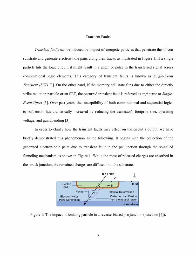
Transient faults can be induced by impact of energetic particles that penetrate the silicon
substrate and generate electron-hole pairs along their tracks as illustrated in Figure 1. If a single
particle hits the logic circuit, it might result in a glitch or pulse in the transferred signal across
combinational logic elements. This category of transient faults is known as Single-Event
Transient (SET) [3]. On the other hand, if the memory cell state flips due to either the directly
strike radiation particle or an SET, the occurred transient fault is referred as soft error or Single-
Event Upset [3]. Over past years, the susceptibility of both combinational and sequential logics
to soft errors has dramatically increased by reducing the transistor's footprint size, operating
voltage, and guardbanding [3].
In order to clarify how the transient faults may effect on the circuit’s output, we have
briefly demonstrated this phenomenon as the following. It begins with the collection of the
generated electron-hole pairs due to transient fault in the pn junction through the so-called
funneling mechanism as shown in Figure 1. While the most of released charges are absorbed in
the struck junction, the remained charges are diffused into the substrate.
Figure 1: The impact of ionizing particle in a reverse-biased p-n junction (based on [4]).
+ -
+ -
+ -
+ -
- +
- +
- +
p+ substrate
p- Si
V+
Electron-Holes
Pairs Generation
Potential DeformationFunnel
Collection by diffusion
from the neutral region
Ion Track
Electric
Fieldn+ Si

3
In particular, if these impinging charges are collected by a sensitive node such as the
reverse biased drain pn junction, it may change the amount of the potential at the drain node and
lead to flipping of the initial state if it is captured by a flip-flop [5] [6]. In addition, by further
reducing the critical charge and the distance between junctions with scaling, the probability of
affecting a single low-energy radiation particle on the output of multiple circuit nodes has
significantly increased. It is anticipated that this trend will continue as long as the technology
scaling occurs and even will get worse by introducing aggressive voltage drop for larger energy
saving in the low-power circuit designs [4]. Thus, the low-power fault-tolerant circuit and system
designs have received significant attention over past years to overcome the scaling challenges
through cost-effective, low-power and high performance fault detection and management
mechanism.
Permanent Faults
Permanent faults are referred to those faults that have continuous impact on the circuit’s
function and may cause the wrong results in the output. Since the permanent faults would not be
vanished prior the entire replacement of defected component, the test technique can be executed
repeatedly to find the erroneous counterpart while it is expected to observe identical results for
all test iterations. Permanent faults are often the consequence of a malfunction in the
manufacturing process. In other words, if the hardware design differentiates from its
implementation, the unintended difference has the potential to impact the circuit’s output. These
faults may eventually result in the circuit failure such as opens, shorts, leakage, and threshold
voltage shift [7] [8].

4
The probability of circuit failure has increased proportionally with the level of technology
scaling. The main reason is that more transistors can be integrated into the same-sized chip by
downscaling the circuit feature which in turn cause the proportional increase of failure in the
nanoscale circuits. For example, the doping profile fluctuation can result in high deviation of the
transistor threshold voltage. Accordingly, designing highly accurate fabrication devices for
addressing the major group of permanent faults resulting from imprecise manufacturing is
paramount to successful deployment of future reliable systems with deeply-scaled devices
operating at low voltages.
Degradation Effects
Even though if we assume that the circuit has been fabricated precisely and package
shielding protects it against both SET and soft errors, the active circuit may still fail due to
reliability issues associated with the activity factor of the circuit. For example, the interconnects
of the circuit can experience gradual movement of ion in the metal because of momentum
transfer from electrons [9]. This phenomenon is referred as electromigration which eventually
cause the failure of the affected circuit. Although the continuing miniaturization of the electronic
devices has significantly reduced the gate capacitance and supply voltage which in turn cause the
current reduction, but the demand for performing the required function with higher frequency has
constrained the current density. On the other hand, the metal line width is proportionally
reduced with shrinking the technology node which result in increasing current density in the wire
cross-sectional area [9].

5
Beside the electromigration concern in the interconnections, the transistors are also
subject to another reliability issues associated with aging-related degradations. Negative Bias
Temperature Instability (NBTI) and Hot Carrier Injection (HCI) are two major aging degradation
threats that can manifest themselves as delay increase which might result in timing errors in the
critical or near critical paths of the circuit [10]. In addition, the High-K/Metal Gate utilization in
the structure of transistor has given rise to Positive Bias Temperature Instability (PBTI) along
with NBTI [11]. Generally, the above transistor aging effects cause a cumulative degradation in
the threshold voltage Vth, of both nMOS and pMOS transistors which leads to slower circuit
operation over its lifetime. If such delay degradation is not budgeted or compensated for, then
the circuit eventually fails to perform correctly within timing constraints. A common
methodology in the consumer electronics market is to under-clock the circuit as compared to
what it was designed to operate under ideal conditions. However, this worst-case approach may
not feasible for all application domains and in most cases, the maximum possible performance is
sought.
Figure 2 shows the lifetime of the circuit implemented by different technology nodes.
The normal execution period has gradually reduced by moving towards downscaled technology
node due to increasing probability of failures such as oxide wearout, electromigration, and aging
effects in the deeply-scaled circuits.
The BTI Phenomenon
Generally speaking, the NBTI is considered the primary source of reliability issue in the
submicron manufacturing era before the technology advancements enable us to fabricate the

6
transistors with sub 28nm technology node. Yet, the utilization of High-K material in the sub
28nm transistor’s structure for maintaining the drain current while improving the oxide
capacitance has changed the ratio of PBTI contribution to the BTI issue. The performance
degradation due to PBTI is gradually increasing as the technology rapidly scales down. We
briefly describe what circumstances result in the NBTI and PBTI phenomena in the next section.
Figure 2: Increasing failure ratio due to accelerated transistor aging (1) and vulnerability to soft
errors (2) [12] [13].
The NBTI Process and its Impact on the Circuit’s Lifetime
Two generally accepted assumptions for Vth shift in the aged circuit, which are also
coincide with the scientific observations are as following: 1) the generation of hole trapping in
the dielectric bulk [14], 2) the break Si-H bonds at the gate dielectric interface due to the
interaction between holes in the inversion layer and hydrogen-passivated Si atom [14] [15]. The
second assumption can also create positively charged interfacial traps and release neutral H
atoms [15]. The generated hole trapping in the dielectric bulk, the broken Si-H bonds and the
positively charged interface traps at the gate dielectric interface due to NBTI stress have been
shown in the Figure 3. It has been reported in [15], [16], [17], [18], [19], [20] that the NBTI

7
effect on the lifetime operation of the circuit is a function of runtime parameters such as
temperature, signal probability, duty cycle, and voltage profile.
It is worthwhile to mention that even the NBTI stress results in the performance
degradation in the system, the device under NBTI stress is entered to the recovery phase while it
is turned off [14]. The recovery phase of NBTI has been investigated by various researcher [21],
[22], [23]. The authors of [23] reported that the stressed device can partially recovered after
stress removal. On the other hand, [22] showed that the stressed device exhibits complete
recovery by switching the device off. The recovery phase starts by returning the freed H atoms
towards the dielectric interface and alleviating the broken Si-H bonds as shown in Figure 3, thus
the absolute value of the Vth is reduced [14].
Figure 3: The NBTI stress and recovery illustration (based on [14] and [24]) .
Figure 4: The PBTI stress and recovery illustration (based on [14] and [24]) .
8
The PBTI Process and its Impact on the Circuit’s Lifetime
Even though the NBTI has been recognized as the major source of the transistor
degradation, the gradual rising performance degradation due to PBTI has undermined the
benefits of introducing High-K/Metal Gate for improving the oxide capacitance. The operation
of this relatively new material under either stress phase or recovery phase is not still entirely
clear to the researchers. However, it is generally accepted that the threshold voltage of nMOS is
shifted under stress condition because of electron trapping at the gate dielectric interface as
illustrated in Figure 4 [24] [25]. Nonetheless, the Vth degradation is partially or completely
alleviated by diffusing back the trapped electrons towards the dielectric interface in the recovery
phase [25].
The BTI Physics and Aging Model
For BTI, the contribution of interface traps and traps inside the dielectric layer are
addressed. Both a Charge Trapping/Detrapping (TD) model and a Reaction-Diffusion (RD)
model have been utilized in the literature to account for these effects [26]. For instance, compact
modeling of aging under DVS for both TD and RD mechanisms is presented in [27].
The Eq. 1 expresses the stress-time induced contribution of Interface Traps (IT) to the Vth
shift [28]:
C
dsgs
A
thgs
ox
aITth tVVEBVV
tKT
EtV )],(.exp[)]()[exp(~)(,
(1)
along with Oxide Traps (OT) inside the dielectric [Tudor et al. 2011]:
9
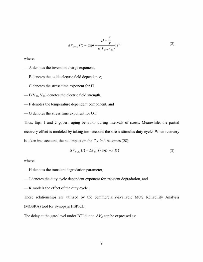
G
dsgs
OTth tVVE
T
FD
tV ).),(
exp(~)(,
(2)
where:
— A denotes the inversion charge exponent,
— B denotes the oxide electric field dependence,
— C denotes the stress time exponent for IT,
— E(Vgs, Vds) denotes the electric field strength,
— F denotes the temperature dependent component, and
— G denotes the stress time exponent for OT.
Thus, Eqs. 1 and 2 govern aging behavior during intervals of stress. Meanwhile, the partial
recovery effect is modeled by taking into account the stress-stimulus duty cycle. When recovery
is taken into account, the net impact on the Vth shift becomes [28]:
).exp().()(, KJtVtV thACth (3)
where:
— H denotes the transient degradation parameter,
— J denotes the duty cycle dependent exponent for transient degradation, and
— K models the effect of the duty cycle.
These relationships are utilized by the commercially-available MOS Reliability Analysis
(MOSRA) tool for Synopsys HSPICE.
The delay at the gate-level under BTI due to thV can be expressed as:

10
))](([)(
tVVV
VCtD
ththDDi
DDi
i
(4)
where, i is a constant which is dependent on the area of the gate, iC is the effective load
capacitance of the gate and α is the saturation velocity index. Clearly, an increase in transistor’s
thV from the initial value thV results in an increase in the delay at logic gate-level.
Categories of BTI Mitigation Methods
Over the years, many techniques for compensating transistor aging have been presented
in the literature. They range from static design-time approaches to dynamic runtime management
approaches. Most approaches will result in some area, power, or performance overheads, while
others try to leverage idle-time of the applications to mitigate aging through power-gating. Most
design-time approaches depend on the use of predictive aging models to proactively decelerate
the aging process within the circuit. However, such design-time modeling can be complicated as
it requires an estimate of runtime operating conditions including input workload.
Figure 5: Proactive vs. reactive techniques [12].

11
On the other hand, the dynamic runtime anti-aging schemes are introduced to avoid the
incurred overheads of pro-active scheme. These reactive adaptation techniques require some sort
of on-chip feedback management system to assess transistor-aging during operation. Figure 5
shows the circuit lifetime implemented by proactive and reactive adaptation techniques whereby
the reactive techniques remain deactivated until the aging rate passes a threshold while the
proactive adaptation technique maintain the aging ratio as low as possible prior to reach the
aging threshold.
Contribution of Thesis
Based on the vast investigation on the previous BTI prediction and mitigation techniques,
a comprehensive survey for some related techniques will be presented in the following chapters.
Our focus will be to classify the existing research works based on their contributions into three
categories: 1) BTI aging prediction, 2) BTI aging measurement, and 3) BTI aging mitigation.
First, the previous BTI prediction techniques are reviewed which are utilized to estimate the
amount of performance degradation over the operational period of a device. Next, we discuss
existing aging-detection sensors which are used to enable the real-time aging-compensation
mechanisms through actively monitoring the transistor parameters or performance degradation.
A concise survey of BTI aging mitigation techniques will be presented after the aforementioned
sections to provide a conceptual overview to the reader.
Furthermore, we will investigate the effect of BTI on the elements utilized in the power-
gating technique which is one of the well-known BTI mitigation methods. Power-gating reduces
the duration of the circuit operation and hence power consumption as well as temperature, both
12
of which can decrease BTI effects. Furthermore, the stress interval of MOS transistors is reduced
because a power-gated MOS transistor enters a recovery condition due to clearing of interfacial
traps. In order to utilize power-gating techniques, a transistor inserted into the header and/or
footer called a Sleep Transistor (ST) is inserted to realize a pull-up and/or pull-down supply
network to provide a virtual VDD or VSS. The ST reduces the leakage current that flows in the
supply-ground path when the circuit is in its stand-by mode which is known as sleep mode.
However, the ST suffers continuous BTI stress during active mode and can age significantly. The
aging impact will aggravate the performance degradation of the logic circuit in a power-gating
structure. NMOS devices exhibit a smaller threshold voltage shift than PMOS devices under the
effect of NBTI [29]. Conversely, PBTI on NMOS can be the dominant degradation mechanism.
Accordingly, the power-gating model used in order to mitigate a BTI effect is important. The
comparison results among different ST implementation are elaborated in chapter five.
To address all these concerns, we will introduce an adaptive resource management anti-
aging approach at the circuit level with low overhead. Essentially, each critical logic path is
determined and remodeled at design-time based on the allowable area overhead, performance
requirements and the expected level of reliability. During the circuit’s operation, only one
instance in the pool of identical logic paths is selected for executing the required function. Each
instance selected from the pool of identical logic paths across the entire circuit is equipped by a
sensor which continuously monitors the aging pace in that particular instance. If a timing
violation occurs in a particular instance, the aged logic instance is power gated while another
identical instance from the pool is selected for continuing the operation of the aged instance. A
detailed elaboration of the proposed technique will be provided in Chapter 6.

13
Organization of Thesis
This thesis is organized into seven chapters. Figure 6 outlines the materials that each
chapter covers. We elaborate some aging prediction techniques in which the lifetime reliability
of the circuit is characterized in Chapter 2. The aging measurement techniques utilizing either in-
situ sensors or replica circuits for circuit degradation assessment are introduced in Chapter 3.
Chapter 4 discusses the related works for mitigating the effect of BTI. The impact of BTI on the
elements used in power-gating technique is introduced in Chapter 5. The power consumption and
delay degradation associated with employment of different power-gating techniques are also
provided in this chapter. Chapter 6 introduces the technical detail of the proposed adaptive
resource management anti-aging approach. Chapter 7 concludes the thesis.
Figure 6: Organization of Thesis
Chapter 1
Chapter 2
Chapter 3
Chapter 4
Chapter 5
Chapter 6
Chapter 7
Need for
Reliability Strategies
The BTI
Phenomenon
Contribution
of Thesis
The Aging
Prediction Techniques
The Aging
Measurement Techniques
The Aging
Mitigation Techniques
Worst-case
Design
Dynamic
Operating
Adaptive Res.
Management
Power-gating for Aging
Mitigation Techniques
Reactive RejuvenationEnergy
Analysis
Area
Overhead
Delay
Evaluation
Technical SummaryTrading Area
for Energy
Tech. Insights
GainedFuture Work
Power-gating
ScenarioVth Analysis
Delay
Evaluation

14
CHAPTER TWO: THE AGING PREDICTION TECHNIQUES
The main objective of the aging prediction techniques is to characterize the lifetime
reliability of the circuit at design-time. Some research works have also integrated their aging
model into the Statistical Timing Analysis (STA) framework to optimize the design timing using
conventional design EDA tools. Accommodation of factors such as process variation, signal
probabilities, etc. into STA help in automation of the process of design-time guardbanding using
area, voltage, or frequency margining [30], [16]. Generally, this worst-case accommodation
results in high overheads.
Aging-aware logic synthesis is also conducted by using multiple timing constraints based
on estimated aging rates. A comparison between various aging prediction techniques has been
shown in Table 1. The comparison between various approaches is done based on the number and
nature of parameters considered during the modeling of aging degradation over time, and
whether the technique is feasible for integration into conventional EDA toolchain, which is key
for easy adoption of the techniques. The large number of parameters required for the models,
requires the use of complex optimization techniques.
In [30], the effects of both fabrication-induced process variation and runtime aging are
considered in the statistical gate delay aging model. While the integrated circuit is fabricated, the
variation in the transistors’ specifications results in producing the circuit paths made by non-
uniform transistors having variable initial threshold voltage and oxide thickness. The random
nature of process variation results in the impact of NBTI on the lifetime performance of the
circuit also becomes a random process. In order to represent the random impact of NBTI aging

15
process, the stochastic collocation method [31] is integrated into the proposed gate delay model
while the parameters of process are considered as random variables with normal distribution.
This consideration enables the proposed STA framework to accurately estimate the lifetime
reliability of the circuit by extracting the correlation among the selected path under stress and
process parametric variations.
The authors of [16] enhanced the aging model at the gate level by taking the workload
information at the gate inputs into account along with other influential aging parameters such as
operational lifetime, temperature, and supply voltage. The workload information is dependent
on the signal probability and transition density. This information is given to the gate delay model
to precisely profile the gate performance degradation while the transistor is under stress
condition. In order to make the proposed model applicable for aging estimation in the multi-stage
gates such as AND and OR, the signal probability and transition density for the internal nets of
the gate needs to be considered. Accordingly, this method splits each multi-stage gate into
several single-stage gates and utilizes a probabilistic method to calculate the aforementioned
parameters for the internal nets of the decomposed gate. Furthermore, they have extended their
approach from gate granularity to Macro Cell granularity to speed-up the timing analysis of the
entire circuit by reducing the timing graph which represents the timing model of the circuit.
Basically, the pool of elements in the proposed timing graph is constrained to those elements
which belong to the critical or near critical logic path.
The authors of [17] proposed an aging-aware timing optimization technique to target only
a sub-set of critical and near critical sensitizable paths for optimization. To identify whether a
path is sensitizable or not, the timed automatic test pattern generation (timed ATPG) [32] is

16
employed to feed the circuit with the combination of the potential input patterns. If at least one
input set activates the path, this path is considered as sensitizable path. Next, the SAT solver is
modified to extract the sub-circuit that covers all possible sentisizable paths. To minimize the
circuit delay due to BTI reliability issue, the proposed algorithm iteratively applies the logic
reconstruction and pin reordering [33] on the critical sub-circuit while the transistor resizing and
path sensitization are considered. As a result, a significant portion of gates are excluded from the
optimization process which makes this approach runtime efficient and highly scalable while
incurring low area overhead.
The proposed idea in [18] is inspired by the fact that currently used synthesis approaches
balance the circuit timing at design-time without considering the impinging delay due to aging
issue for each path. In this regard, the paths with larger timing slack are slowed down for
balancing the delays which relatively saves the area. However, the area reduction of these paths
come at the expense of increased aging ratio whereby the non-critical paths might become
critical over the circuit’s operational lifetime. To improve the overall lifetime of the circuit, the
aging-sensitive paths are redesigned to be executed faster which incurs more area overhead to the
system. To compensate this overhead, the paths with shorter timing slack are redesigned to be
executed slower while their timing constraints are correspondingly relaxed. Thus, the
consideration of the post-aging delay while optimizing the circuit timing significantly improves
the overall lifetime of the aging-susceptible circuit which results in all paths reach the desired
guardband at the same time.
An additional design-time technique of aging-aware logic synthesis is proposed in [34]
where multiple timing constraints are applied on different logic paths based on the available

17
timing slacks and aging rates. The key innovation of this work is to synthesize microprocessor
pipeline stages which are balanced in terms of Mean-Time-to-Failure (MTTF) instead of the
traditional approach of delay-balanced pipelines. Here, tighter timing constraints are obtained
through a combination of gate-sizing, logic path re-organization or time borrowing or by using
low-Vth gates.
The beauty of the proposed technique in [19] is that the runtime variation at the system-
level granularity is extracted to enhance the accuracy of delay estimation in the circuit-level
granularity. To achieve this goal, the target application is executed on a full computer simulator
to capture the workload profile including input pattern and power information. Next, the logic
simulator is fed by workload profile and gate-level netlist to extract the signal probability and
switching activity of each transistor. Then, the voltage and temperature at gate-level granularity
are obtained based on the provided information from the previous step to accurately estimate
each gate delay due to induced BTI. As a result, the circuit delay can be accurately estimated by
considering the gate delay as a function of Vth shift, temperature and voltage in the STA tool. The
integration of this framework into commercial EDA tool chain can provide the scalability for
large-scale circuit designs. In addition, the proposed automated aging analysis methodology
demonstrated in [20] enables the circuit designers to benefit from the fast and highly accurate
aging prediction methodology which has also been integrated into the commercial STA tool
(Synopsys PrimeTime).
The iterative optimization process through the use of commercial synthesis tools is
attractive, although the authors report in [18] that it may not converge and the area overhead may
be excessive in some cases. Furthermore, such High-Level Synthesis (HLS) techniques [35]

18
assume the availability of a standard cell library characterized with aging delays which can guide
the synthesis process to utilize optimal-sized/-Vth logic gates such that desired lifetime is
achieved.
Table 1: Comparison of aging prediction techniques.
Aging Prediction Technique Considered Parameter in the Model
Integration into
Commercial Tool
Identified
Lu et al., 2009 [13, 30]
temperature, signal probability, duty
cycle, process variation, voltage
variation
no
Lorenz et al., 2010 [16] temperature, signal probability, circuit
lifetime, workload profile no
Wu et al., 2011 [17] temperature, signal probability, circuit
lifetime no
Ebrahimi et al., 2013 [18] temperature, signal probability,
switching activity, circuit lifetime yes
Firouzi, Kiamehr, Tahoori, et
al., 2013 [19]
temperature, signal probability,
switching activity, power-voltage
profile, workload profile
yes
Karapetyan et al., 2015 [20]
temperature, signal probability,
transistor density, circuit lifetime,
voltage profile
yes

19
CHAPTER THREE: THE AGING MEASUREMENT TECHNIQUES
Some anti-aging techniques downplay the use of aging prediction through the use of on-
chip sensors for in-field measurement of transistor aging. Many aging sensors have been
proposed in the past to accurately monitor the transistor parameters or performance degradation
of the active devices. The proposed aging sensors can be categorized from those based on Metal–
Oxide–Semi-Conductor Feld-Effect Transistor (MOSFET) parameter sensing [36], to those that
are rely on propagation delay measurement through ring oscillator [37], [38], [39]. The output of
these aging measurement techniques can be used as a control signal in the aging-mitigation
methods to overcome the performance degradation due to aging phenomena. In addition, the on-
chip aging sensor is required to exhibit low sensitivity to PVT (process, power supply voltage
and temperature) and impose reasonable area overhead to the circuit design [39].
Initially, in order to measure the BTI effect, the BTI-induced parameters were directly
sensed. Although this early stage technique was efficient in the beginning, the researchers
understood over time that the direct MOSFET parameter sensing can introduce the large
recovery while characterizing the BTI effect. Thus, the BTI measurement techniques which
introduce zero recovery while determining the actual degradation under BTI stress became
favorable. The proposed BTI sensor in [36] works through monitoring the small voltage drift via
on-the-fly measurement without having recovery effect on the sensed transistor. However, this
technique requires off-chip measurement circuits such as voltage reference which makes it
potentially unfavorable for utilizing in the circuits with limited power budget.

20
On the other hand, instead of measuring the BTI directly, the propagation delay can be
considered as an expression of the BTI effect. In [40], an on-chip sensor which monitors the
frequency degradation of the circuit is presented. The two Ring Oscillators (RO) are devised to
be employed in the structure of this sensor device. The reference RO is considered as the
reference to determine the amount of frequency degradation in the stressed RO. Accordingly, the
reference RO is kept unstressed while the other RO is periodically stressed. In particular
timestamp, the phase comparator is activated to measure the frequency difference between these
two ROs. This comparator produces a beat signal which represents the frequency proportional to
the aging effect. Next, the generated beat signal is fed to a counter to quantify the amount of
degradation. The utilization of two ROs in this design improves the sensing resolution by 50X
compared to the limitation of the previous techniques which proposed to only use a single RO in
their structure.
In order to translate the frequency degradation to Vth shift, the calibration methodology
proposed in [31] can be utilized. However, since the BTI-induced degradation cannot be
quantified based on the amount of Vth shift due to NBTI and PBTI, it might not be an appropriate
technique to be employed as sensor for a particular BTI reliability issue. Nonetheless, the same
pair RO architecture is modified by the authors of [37] to separately quantify the aging effects of
HCI and BTI.
The authors of [38] proposed a compact NBTI sensor which works based on the fact that,
by increasing the Vth due to NBTI, the frequency of RO significantly reduces. This sensor
enables the chip testers to digitalize the NBTI stress in the subthreshold region. However, the

21
operation of this design in the subthreshold region suffers from nontrivial sensitivity to
temperature variation.
Recently, the HCI has manifested itself as a critical reliability issue due to manufacturing
transistors with the gate lengths shorter than 50nm [39]. The NBTI/HCI on-chip aging sensor
proposed in [39] measures the threshold voltage difference between a stressed device and fresh
device through the deployment of a threshold voltage detector and a comparator. The proposed
sensor circuit offers a resolution of 1 ns per 0.01 V threshold voltage shift.
The authors of [41] proposed an on-chip aging sensor which is able to isolate the NBTI
and PBTI aging effect. For determining the impact of NBTI, two identical NBTI sensors are
embedded in this design. Again, the delay difference comparison idea between the stressed
sensor and the reference sensor is utilized. Both sensors are fed by a specific duty cycle which
results in the reference sensor remaining isolated from this trigger signal while the other one is
aged. As a results, the longer propagation delay is observed in the aged sensor. In order to
measure the PBTI effect, the same structure is utilized with the difference being that the pMOS
devices are replaced by nMOS devices.
Although the concept of using RO for monitoring aging incurs small area overhead and
zero performance penalty [42], it still cannot adequately represent the operation function of the
circuit which experience the complex workload interdependency over time. To provide an
accurate aging measurement technique, the authors of [42] came up with the idea of resembling
the topology of the critical and near critical paths with Representative Critical Reliability Paths
(RCRPs) which are able to represent the aging in the critical reliability paths. To reduce the

22
overhead of these RCRPs, the resembled critical paths are synthesized to cover those paths which
have the higher degree of shared delay segment.
On the other hand, some techniques have focused on aging-induced performance
degradation to detect sequential circuit timing failures [43], [44]. The objective of these works is
to use time borrowing concept for compensating the timing delay. However, area overheads and
significant power penalties can be incurred using designs with such specialized sequential
elements.
Apart from aforementioned aging measurement techniques, there are some commercial
tools such as [45] which consists of both hardware and software packages required for quick and
accurate BTI test applications, as well as general characterization. Table 2 provides a qualitative
analysis of the aging measurement techniques which will be presented in the final manuscript.
Table 2: Comparison of several aging sensors (as adapted from [41]).
Sensors Sensed Variable NBTI PBTI HCI Objective
Denais et al., 2004 [36] Vth yes no no characterization
Kim et al. 2008 [40] frequency yes yes yes characterization
J. Keane et al., 2010 [37] frequency yes yes yes circuit tuning
Karl et al., 2008 [38] frequency yes no no characterization
K. K. Kim et al., 2010 [39] Vth yes no yes characterization
Alidash et al., 2012 [41] delay yes yes no circuit tuning
Wang et al., 2012 [42] delay yes yes yes circuit tuning
Dadgour et al., 2010 [43] setup time yes yes yes binary fail detection
Qi et al., 2010 [44] delay yes yes no binary fail detection

23
CHAPTER FOUR: THE AGING MITIGATION TECHNIQUES
The main objective of BTI aging mitigation techniques is to compensate the aging-
induced delay in the active circuit. The conventional approach of adding guardbands
significantly reduces the performance of the systems while it also conflicts with the primary goal
of transistor downscaling for delivering higher performance in shorter execution period. Thus,
the focus of the most recent research in this area has been recast to improve the aging-induced
performance degradation without adding the costly overheads to the system.
Figure 7: Taxonomy of aging mitigation techniques.

24
The BTI aging mitigation techniques range from simple one-time static timing margin
and voltage guardbanding, up through more complex dynamic adaptation of supply voltage
and/or frequency during operation. We have categorized the BTI aging mitigation techniques to
three top-level methodologies as shown by the Taxonomy in Figure 7 with details listed in Table
3: 1) Worst-case Design, 2) Dynamic Operating Conditions, and 3) Adaptive Resource
Management. These categories are delineated in [46] to provide a means to compare the
capabilities and performance of alternative aging mitigation strategies.
Worst-case Design Techniques for Aging-Compensation
Voltage-Margin (VM)
Guardbanding has been used to protect against NBTI which accounts for degradation
over the lifetime of a design by reducing the operating frequency or increasing supply voltage, to
eliminate BTI-induced timing violations. Unfortunately, provision of a voltage guardband will
increase energy consumption over the entire period of operation [15]. Accordingly,
guardbanding is known as the worst-case design technique to ensure reliable operation
throughout the circuit lifetime. For instance, timing guardbanding (Frequency-Margin (FM))
selects the clock period to be more than propagation delay of the aged circuit. Such over-design
can also take the form of elevated supply voltage operation (Voltage-Margin (VM)) as high as
14.5% over the nominal voltage of an unaged device [47]. This translates to about 30% increase
in lifetime energy consumption to compensate for NBTI effects alone. The significance of
compensating these overheads is increasing with scaling of technology nodes.

25
Table 3: Comparison of the aging mitigation techniques [46].
Technique Anti-Aging
Strategy
Design
Requirements/
Parameters
Adaptability
Characteristics/
Degree
Overheads
Throughput Power Area
Worst-case Design
VM, FM Static Margin
MD-RoD/
∆VDD,
∆Fnominal
None FM: High
VM: High
(Dynamic &
Leakage)
None
Gate-Sizing Static Margin
MD-RoD; Extended
Std. Lib.;
Multi-obj. Opt./
Δβi, ∀ gates i
None None
Medium
(Dynamic &
Leakage)
Low (Gate-
level)
Re-Synthesis Static Margin
MD-RoD annotated
Std. Lib.;
Aging-aware
Synthesis/ Δβi,
ΔVth,i ∀ gates i
None None
Low-Medium
(Dynamic &
Leakage)
Low (Gate-
level)
Dynamic Operating Conditions
DVFS Dynamic
Margin
Timing Sensors;
Feedback Control/
ΔVDD(t), ΔF(t),
ΔVbb(t)
Yes/ Fully
Autonomous Low
Medium
(Dynamic &
Leakage)
Medium (On-
chip VR &
sensors)
SVS Dynamic
Margin
MD-RoD/
ΔVDD(t +Δtstep) Yes/ tstep None
Medium
(Dynamic &
Leakage)
Medium (On-
chip VR)
GNOMO Static Margin +
Power-Gating
MD-RoD/
(VDD,g, tidle) None
Medium
(Workload
Dependent)
Medium
(Dynamic &
Leakage)
None
Adaptive Resource Management
SD Proactive Mngt.
+ Power-Gating
Modular
Redundancy/ Sleep
Interval
Yes/ Sleep
Interval None
High
(Leakage)
High (Module-
level)
ITL schemes Proactive Mngt.
+ Power-Gating
Exploit App.
Redundancy/
Idle time
Yes/ Task
Scheduling
Medium
(Workload
Dependent)
None None
LWL
Proactive Fine-
Grain Mngt. +
Power-Gating
CPRT/ Sleep
Interval
Yes/ Sleep
Interval None
Minimal
(Leakage)
Low (Gate-
level)
RR
Proactive Fine-
Grain Mngt. +
Power-Gating
Timing Sensors;
Feedback
Control; CPRT/
ERT%
Yes/ Fully
Autonomous None
Minimal
(Leakage)
Low (Gate-
level &
sensors)
MD-RoD: Model-Dependent Rate of Vth Degradation
VR: Voltage-Regulators

26
Gate-Sizing
Other worst-case design techniques which utilize additional area to compensate for aging
effects include gate-sizing techniques [48] [49]. As indicated by Eq. 4, the delay at gate-level can
be decreased by increasing the gate size Δβi from its minimal allowable size βi. Thus, gate-sizing
techniques involve finding optimal sizes for all gates within an allowable discrete or continuous
range in the circuit synthesis stage such that all the logical paths meet the desired timing
specifications throughout the lifetime. The complexity of discrete gate-sizing is known to be NP-
complete, thus mostly heuristics are utilized [50]. Furthermore, this aging-aware synthesis is
performed based on assumptions such as knowledge of the stress probabilities at all nodes in the
circuit and provision of a standard cell library having logical gates with multiple widths for each
stress level. For example, an area overhead of 19.8% is reported for gate-sizing selected portions
in a physical register file of a SPARC processor [51]. The area overheads associated with sizing
at the gate level can be reduced by adopting more fine-grain sizing and considering the impact of
adjacent gates [52], however, it increases the complexity of the sizing problem.
In addition to the area overhead associated with gate-sizing techniques, the increased
gate-widths contribute to increasing the effective gate capacitance thereby increasing the
dynamic power consumption of the circuit. Furthermore, the gate leakage and subthreshold
leakage currents are also dependent linearly on the width of the gates. Hence, gate-sizing
schemes directly contributes to both dynamic and leakage powers. Thus, the gate-sizing problem
becomes more complicated as these factors also need to be considered during the optimization
process. The over-sized gates also undergo continuous stress in the form of elevated temperature

27
and high signal activities depending on the input conditions while no opportunity for forced
recovery is pursued.
Dynamic Operating Conditions for Aging-Mitigation
A significant drawback of design-time techniques is that they require accurate estimation
of aging using anticipatory models such as RD or TD as described earlier, whose accuracy is still
under investigation by the research community [53]. The models have only been verified at the
individual logic-gate level or on ring oscillator circuits. The authors are not aware of any study
which evaluates the accuracy of these aging models on benchmark or real-use-case circuits. Most
design-time techniques rely on these models to lower their associated overheads, such as the area
overheads of gate-sizing techniques. Thus, in practice over-estimation is used to accommodate
the circuit lifetime. Herein, the devised techniques give the explicit provision of control over the
delay degradation via the novel control knob of sleep interval and hence eliminates the need of
accurate aging estimation.
Dynamic Voltage and/or Frequency Scaling
To overcome the constant overheads associated with voltage guardbanding, the voltage
can also be increased gradually from its nominal value at run-time to compensate for delay
degradation due to aging (see Eq. 4). In this case, supply voltage can be dynamically adapted,
VDD(t), to prevent any aging-related failure based on feedback mechanisms whereby aging is
monitored using canary circuits or tunable replicas [42], [54]. These canary circuits are assumed
to assimilate wearout of the original circuit. On the other hand, timing sensors can also be placed

28
into the circuit for this purpose [55]. Based on the feedback provided, multiple control policies
are devised in [56], [57] to jointly tune parameters such as voltage, operating frequency and
dynamic cooling to maximize lifetime energy-efficiency.
Alternatively, if the provision of a feedback mechanism is not available, then Scheduled
Voltage Scaling (SVS) can be performed whereby the voltage increments and time steps Δtstep are
determined at design-time [47]. However, DVS is shown to achieve a lifetime (10 years) energy
benefit of only 7% with respect to simple guardbanding [58]. Additionally, such schemes assume
the availability of a mechanism which can achieve voltage steps on the order of 5-10mV, which
require high area-overhead and power inefficient on-chip voltage regulators.
Yet another technique to dynamically mitigate Vth degradation is Adaptive Body Biasing
(ABB) [59], where the body-biasing voltage Vbb(t) is adapted based on feedback at the transistor
level. However, it can be less effective with increased levels of degradation and needs to be
combined with other techniques such as SVS and aging-aware synthesis [60].
Computational Sprinting
An effective aging-mitigation technique Greater-than-NOMinal Operation (GNOMO) is
proposed in [61] which eliminates the need for complex feedback-based control policies and/or
on-chip voltage regulators. As proposed herein, aging recovery is similarly promoted through the
use of power-gating. However, to lower the throughput degradation due to power-gating, the
circuit is operated at elevated supply voltage, VDDg > VDD, to increase throughput during bursts
followed by idle periods tidle generated to ensure recovery via power-gating. These circadian
rhythms were shown to reduce delay degradation by about 1.3-fold to 1.8-fold.

29
Even though static or dynamic guardbanding in the form of voltage/frequency margining
are effective techniques to combat aging, which do not require any changes at the circuit-level
[58]. However, the energy overheads due to static margining are generally high, and the
implementation complexities of dynamic margining schemes are also high [53]. To address
aforementioned issues, low-complexity and low-overhead anti-aging strategies based on adaptive
resource management at the circuit-level will be introduced in the next section.
Adaptive Resource Management for Aging-Resilience
In this sub-section, a class of anti-aging schemes are highlighted whereby the rate of
degradation is balanced over all the resources in the circuit either through management of idle
time and task scheduling or availability of expendable resources. Aging-mitigation in these cases
include power-gating to enforce recovery, or applying specific input vectors which promote
recovery or using differential voltage scaling. Power-gating can reduce degradation of Vth by
lowering probability that the transistor is under stress.
Idle-Time Leveraging (ITL) Schemes
As mentioned earlier, power-gating has been effectively shown to mitigate transistor
aging effects. Schemes such as clustered power-gating [62] have proposed effective ways to
reduce the overheads of power-gating, whereby the critical and non-critical portions of the circuit
are power-gated using different-sized sleep transistors. However, such works assume the
availability or prediction of circuit downtime. For instance, tradeoff analysis between lifetime
extension and leakage reduction for a 4x4 Network-on-Chip switch [62] show that with the sleep
30
probability ranging between 0.4 and 0.9, it is possible to increase the lifetime between 2.5X and
6.67X.
In other applications like modern microprocessor cores, the inherent redundancy in
certain structures like the pipelined Execution Stage which has multiple arithmetic units can be
exploited [63]. Aging mitigation in this scenario can be achieved by carefully scheduling tasks
onto the available resources while simultaneously recovering aging effects through power-
gating. However, this comes at a cost of throughput degradation as the power-gated units are
unavailable to realize maximum Instruction-Level Parallelism (ILP). Thus, the amount and
distribution of idle time is highly dependent on application characteristics and may require
changes at the instruction-sequencing level to realize full benefits as reported by authors.
Similar resource scheduling at a much coarse-grain level has been demonstrated for
multicore processors [64] or General-Purpose Graphics Processing Units (GPGPUs) [65],
whereby tasks are assigned based on stress information at core-level. At runtime, workload
assignment is done such that cores are relaxed periodically. The NBTI-aware task mapping for
multicore processors is shown to improve MTTF by 30% under considered workloads [64]. Here
again, availability of both idle time and idle cores is assumed, which is dependent on the
application characteristics or workload.
Some other techniques which assume the availability of idle (standby) time involve
applying design-time generated input vectors which promote recovery [66]. In summary, the
aforementioned schemes typically require control strategies at hardware/software level to
dynamically detect idle times during dynamic operation and perform the required aging-
mitigation.

31
Controlled Resource Wearout to Improve Performance
The BubbleWrap scheme [67] for many-core systems proposes control strategies with the
goal of optimizing either power or performance while managing the amount of aging at the core-
level. It utilizes a combination of DVS and task scheduling schemes to overcome the throughput
degradation. A set of throughput cores, which are utilized for parallel sections of application and
expendable cores, which are utilized for sequential sections of application are assumed. These
two subset of resources are created based on the rate of degradation of individual cores. The
expendable cores, which have shorter life are expended earlier using elevated voltages to obtain
higher application performance. Alternatively, the set of throughput cores can be expended for
the same power budget, where aging for expendable cores is managed by using voltages below
VDD. The BubbleWrap scheme has similar concerns as found in other DVS schemes and assumes
availability of extra resources which can be worn-out.
Structural Duplication (SD)
The enhancement of logic reliability via indiscriminate Structural Duplication (SD), as
demonstrated in [68] can result in prohibitive area overheads. In particular, the approach
identified functional elements at a module-level granularity for instantiation as standby
components to facilitate an increase in device lifetime. In case of a failure, the standby element
can be activated resulting in increased lifetime. Structural duplication is considered feasible only
if 100% area cost is acceptable.

32
Logic-Wear-Leveling (LWL)
It is possible to utilize fine-grain gate-level redundancy for reducing energy consumption
which results in incurring significantly less area overhead. The Logic-Wear-Leveling (LWL)
technique [69] uses a novel synthesis technique called Critical Path Replication Tool (CPRT) to
replicate only the timing-critical logic paths rather than the entire circuit as a whole. Next, the
LWL activates each instances with a round-robin fashion for a certain period while power-gating
the unselected critical path instances. By removing the stress condition in the unselected
instances, the timing degradation due to BTI is mitigated in the power-gated logic domains.
Thus, the wear-leveling effect obtained via proactively alternating between redundant critical
paths can save up to 31.98% energy consumption at 10 years compared to the traditional voltage
guardbanding.
Reactive Rejuvenation (RR)
The Reactive Rejuvenation (RR) technique [1] deploys a simple shadow latch based
timing sensor [70] to examine the BTI impact throughout the lifetime operation of the circuit.
The output data is sampled in two different points in time whereby the earlier sample is stored in
the main latch while the latter sample is captured by the shadow latch operating with a delayed
clock signal as illustrated in Figure 8. Thus, the aging-induced timing violation can be simply
detected by a comparison operation using a simple XOR logic gate. By detecting any timing
violation in the circuit, an error signal is generated to trigger the feedback device controller for
compensating the aging effect. This reactive function block shown in Figure 9, removes the

33
stress condition in the currently active logic domain by putting it on the sleep mode while
another unaged identical critical logic instance remodeled using CPRT is activated with a round-
robin pattern to continue the function of the aged instance. This design can achieve the delay
degradation reduction by a factor of 3.32X compared to uncompensated design.
Figure 8: Sampling the output data at two different points in time [1]
Summary
Transistor-aging is a growing reliability concern in deeply scaled devices, which is often
mitigated through design-time approaches, which results in constant high overheads. A
comprehensive survey of all techniques presented in the literature is to be done and a taxonomy
is to be developed. We seek a technique which can limit the overheads of worst-case modeling
through low-overhead dynamic monitoring based on circuit parameter and resource
management. The feasibility of integration of the approach in current EDA tools is also essential
to foster the full benefits. Addressing these reliability concerns is paramount to successful

34
deployment of future reliable systems with deeply scaled devices operating at low-voltages.
Based on our background, we presented a comprehensive survey.
Figure 9: Autonomous aging-aware resource management for N = 2 [1, 12]

35
CHAPTER FIVE: POWER-GATING STRATEGIES FOR AGING
MITIGATION OF CMOS LOGIC PATHS
In order to utilize power-gating techniques, a transistor called a Sleep Transistor (ST) is
inserted into the header and/or footer to realize a pull-up and/or pull-down supply network to
provide a virtual VDD or VSS. The ST reduces the leakage current that flows in the supply-
ground path when the circuit is in its stand-by mode which is known as sleep mode. However,
the ST suffers continuous BTI stress during active mode and can age significantly. The aging
impact will aggravate the performance degradation of the logic circuit in a power-gating
structure [71]. NMOS devices exhibit a smaller threshold voltage shift than PMOS devices
under the effect of NBTI [29]. Conversely, PBTI on NMOS can be the dominant degradation
mechanism. Accordingly, the power-gating model used in order to mitigate a BTI effect is
important.
In order to alleviate aging of ST, several works have been presented previously. The
authors of [72] proposed to realize NBTI-aware power-gating through (i) sleep transistor
over-sizing, (ii) forward body-biasing, and (iii) stress time reduction. However, the aging of
logic networks has not been considered in that work. In [73], authors showed the
interdependence between the degradation or logic networks and the ST. In their work,
redundant STs are introduced for mitigating the aging of a single ST. This is shown to extend
the lifetime of power-gated circuits. With the existence of ST redundancy, the recovery
mechanism is explored by recovering redundant STs in a round-robin sequence.
Consequently, a sufficient recovery interval is provided to STs for reversing NBTI. Hence, a

36
decrease in the virtual VDD due to ST aging is postponed, which mitigates the long-term
performance degradation and extends the circuit lifetime. The authors of [74] evaluated the
reliability and power consumption benefits of power-gated circuits in 22nm technology under
the effects of NBTI/PBTI. They found that power-gating can improve the reliability and
provide significant power savings as long as sufficient time for the circuit is provided in sleep
mode. For example, [58] reports that to reduce the delay degradation by 5% over an
operational period of 10 years, the circuit must remain power-gated for over 60% of the
device lifetime which may represent an unacceptable reduction in operational capacity. Thus,
alternative approaches have constituted an active area of research [69].
In this chapter, we show the evaluation of the effectiveness of power-gating on
PBTI/NBTI phenomenon and propose a preferred ST configuration for achieving improved
recovery. In addition, different input frequency signals with the same duty cycle are
considered as a case study to obtain more complete results which include the effect of input
transitions on the recovery of MOSFET transistors while in sleep mode.
Power-Gating Scenarios
There are several possible power-gating scenarios based on the location of the ST in the
header or footer. To evaluate these, a case study is considered using 50 CMOS inverters which
are connected in series, as shown in Figure 10. For the baseline circuit, supply voltage and
ground are directly connected without any ST. We implement three different power-gating
scenarios in order to investigate the impact of BTI on each of them. In the Header-based ST
(HST), we insert a PMOS ST to create virtual VDD as illustrated in Figure 11. Since the PMOS

37
ST in power-gated circuit suffers from NBTI in active mode and ages quickly, it degrades the
performance of logic elements due to supply voltage changes. One advantage of an HST
arrangement is that PMOS transistor exhibits less leakage current than NMOS transistor of
equivalent size. The NBTI effect elevates Vth over time and makes PMOS transistor even less
leaky. The disadvantage of an HST arrangement is that PMOS has lower drive current than
NMOS of a same size. As a result, a HST implementation usually consumes more area than a
Footer-based ST (FST) implementation.
In FST, we insert a NMOS ST between VSS and actual ground, shown in Figure 12. The
advantage of FST is its high drive current and hence smaller area for equivalent performance.
However, NMOS is leakier than PMOS and application designs become more sensitive to
ground noise on the virtual ground coupled through the FST. The NMOS ST also suffers from
PBTI in active mode which imposes additive performance loss. However, the performance loss
of HST and FST circuits is not equal since PMOS ST experiences more dramatic aging effects
when it is used in an HST structure in compare to NMOS ST in a FST design. Consequently,
HST and FST designs both impact the logic network performance in a different way which are
elucidated in this work.
Regarding this observation, we also implement a hybrid power-gating scenario referred to as
Header and Footer ST (HFST). HFST corresponds to simultaneous use of PMOS and NMOS
STs which help to isolate the transistor gate terminals from electric field stress due to application
of inputs during sleep mode. Figure 13 shows HFST design which combines the HST and FST
characteristics in this manner.

38
Input Output
Figure 10: The original circuit
VDDSleep
VVDD
Figure 11: The Header-based ST circuit
VVSS
VSS
Sleep
Figure 12: The Footer-based ST circuit
Figure 13: The Header and Footer based ST circuit
A taxonomy of these three alternatives is depicted in Figure 14. It shows the various ST
implementation features in comparison for each technique. For instance, HST and FST are
influenced more by an NBTI effect or PBTI effect, respectively. Since HFST utilizes both
NMOS and PMOS STs in the power-gating implementation, it suffers from both NBTI and
PBTI. Furthermore, the PMOS ST channel width in HST approach should be wider to
compensate for reduced carrier mobility in comparison to NMOS ST. Consequently, HST

39
approach imposes approximately two times larger overhead to the ST. Hence, HFST approach
endures 1X+2X=3X increase in overhead due to use of both PMOS and NMOS ST in its
structure. PMOS ST has a reduced amount of leakage current in comparison to NMOS ST.
Thus, HST design exhibits a lower leakage current than FST design. As a result, HFST takes
advantage of both HST and FST in its implementation and bears a smaller amount of leakage
current.
Figure 14: Taxonomy of ST Arrangements and their characteristics
Experimental Results
To evaluate the above scenarios, the three ST arrangements are subjected to an input
squarewave with a 50% duty cycle having a frequency of 1KHz or 100KHz. Each circuit is
evaluated under conditions whereby it is in sleep-mode for 70% its lifetime. Consequently, the
sleep transistor interrupts the path between the VDD and ground based on ST arrangement. Our
circuit-level modeling is performed via Synopsys HSPICE reliability analysis to simulate BTI
effect for the 45nm Nangate open cell library. In order to apply aging on the inverter chain
ST Arrangement
HST FST HFST
BTI Effects:
Area Penalty:
NBTI
2X
PBTI
X
NBTI and PBTI
3X
Leakage Current: moderatelow low
Vth shift:[3.19,3.98]mV [3.27,4.06]mV [3.09,3.43]mVnMOS
Vth shift:[9.79,9.82]mV [10.46,10.50]mV [9.61,9.64]mVpMOS

40
circuit, we used MOSRA model [28]. The MOSRA model is constructed with physics-based
formulations and augmented with coefficient parameters, to improve the model accuracy and
parameter extraction flexibility as identified in the equations below.
Vth Shift
NBTI/PBTI effects have two phases of operation depending on the bias condition of a
PMOS/NMOS transistor: these are a stress phase and a recovery phase. In the stress phase, the
threshold voltage (Vth) of PMOS/NMOS increases. During the recovery phase, Vth degradation is
partially recovered due to clearing of interfacial traps.
In order to calculate Vth shift, we used the built-in model provided by MOSRA [28]. The
MOSRA threshold voltage degradation model provides results which are accurate in numerous
aging studies. Two principal physical mechanisms are considered in MOSRA: one is related to
the contribution of the interface traps (Equation 5) and the other related to the traps inside the
dielectric layer (Equation 6) which are provided here in abbreviated form. In the equations,
E(VGS, VDS) denotes the strength of the electric field of the dielectrics. Regarding to the
significant dependence of NBTI and PBTI on the channel length, flexible channel width- and
length-dependence equations are included in the BTI model of MOSRA.

41
The partial-recovery effect is modeled by taking into account the stress stimulus duty
cycle. When the partial-recovery effect is considered, the total degradation becomes smaller:
where the g quantity models the effect of duty cycle. As shown in Figure 15 and Figure 16 Vth
shift in the power-gated circuits is less than the baseline circuit. Moreover, Vth shift in the
baseline circuit rises rapidly over time while power-gated circuits have a rather smooth Vth shift.
The reason is that the power-gated circuits are in sleep mode 70% of the time which results in
much less stress than the baseline circuit. So, during sleep mode, only the recovery phase
impacts aging and decreases the aging-induced threshold voltage shift.
Delay Penalty
Typically, sleep transistors are sized such that a tradeoff among voltage drop, leakage
savings, and area overhead is obtained [71]. At the beginning of the device lifetime, addition of a
ST will increase the delay. However, the delay penalty decrease as the size of the ST is
increased. In this research, the ST has been chosen in a way that the increased delay of the
power-gated circuits is less than 3% as compared to the delay of the baseline circuit and the
NIT
dags
TITCE
THgs
x
a
ITTH tVVETITFDVVtTK
Ev .,.exp..
.exp
0
,
(5)
NOT
dsgs
OTTH tVVE
T
TOTTDTOTFD
v .,
exp,
(6)
gTDCDvTTDv THACTH .exp..0, (7)

42
leakage current is optimum. When we compare the delay of the three circuits, we find that the
power-gated circuits have higher delay within 2 years as compared to the baseline, as shown in
Figure 17 and Figure 18. However, the power-gated circuits suffer less from aging after 2 years
due to the reduced Vth shift.
Figure 15: Comparison of increased Vth for 100KHz signal
Figure 16: Comparison of increased Vth for 1KHz signal

43
Figure 17: Comparison of increased delay for 100KHz signal
Figure 18: Comparison of increased delay for 1KHz signal

44
Input Vector Impact on BTI Recovery
It has been assumed that the circuits operate all the time yet practically, not every
application requires the underlying hardware to operate at highest performance level all the time.
There are periods during which the circuit is not in use, but still affected by the stress induced by
the electric field from the application of inputs over a path to ground. This results in the
PMOS/NMOS transistors being either under stress or recovery conditions. Although power-
gating of portions of the circuit which are not in use may decrease Vth shift, although doing so
does not completely recover PMOS/NMOS transistors since they are still under input stress.
Figure 19 and Figure 20 demonstrate the comparison of Vth shift for the first three PMOS and
NMOS transistors of the Circuit Under Test (CUT) within the inverter chain. The CUT is
evaluated in the HST design for 100KHz input signal. The Vth shift for PMOS transistors is
around three times greater than Vth shift for NMOS transistors due to further impact of NBTI on
PMOS transistors rather than PBTI on NMOS transistors. Moreover, as illustrated in Figure 19,
initial transistors in the CUT experience increased aging compared to subsequent transistors,
depending on if the circuit is in the sleep mode.
Analysis and Conclusion
Table 4 shows the comparison of the delay degradation for the circuit which is equipped
with different ST arrangements. The delay degradation is between 3.14% and 3.72% for all
circuits within the first 2 years of their lifetime which indicates that all arrangements are seen to
degrade at similar rates. However, the power-gated circuits suffer less from the aging effect since

45
they benefit from the less Vth shift after two years. As a result, the delay penalty of the power-
gated circuits reduce over time. Table 5 demonstrates power consumption comparison with
100KHz input vector.
Figure 19: Comparison of Vth shift for the first 3 NMOS of CUT
Figure 20: Comparison of Vth shift for the first 3 PMOS of CUT

46
The baseline circuit is influenced further by the aging effect over time which results in
higher Vth shift which reduces the leakage current. Consequently, the trends of power
consumption for the baseline circuit shift more than other methods which have relatively
constant power consumption.
Table 4: Delay degradation Comparison (% baseline)
Time
Method
2 years
(%)
4 years
(%)
6 years
(%)
8 years
(%)
10 years
(%)
Baseline 3.22 4.10 4.48 4.69 4.81
HST 3.72 3.62 3.64 3.54 3.44
FST 3.14 3.17 3.18 3.18 3.18
HFST 3.14 3.16 3.16 3.17 3.18
Table 5: Power Consumption Comparison (in Watts)
Time
Method d
2 years 4 years 6 years 8 years 10 years
Baseline 6.64E-07 6.54E-07 6.47E-07 6.43E-07 6.41E-07
HST 6.81E-07 6.79E-07 6.79E-07 6.79E-07 6.78E-07
FST 6.73E-07 6.72E-07 6.72E-07 6.72E-07 6.71E-07
HFST 6.82E-07 6.82E-07 6.82E-07 6.82E-07 6.81E-07

47
CHAPTER SIX: REACTIVE REJUVENATION OF CMOS LOGIC PATHS
USING SELF-ACTIVATING VOLTAGE DOMAINS
Herein we look toward providing greater improvements in delay degradation, while
decreasing the power consumption utilizing spatial multiplexing. Therefore, in this chapter we
focus on introducing an adaptive resource management anti-aging approach at the circuit level
with low overhead. In this work, it is shown that overheads existing in guardbanding approach is
significantly reduced. Furthermore, an opportunity is provided for aging-critical portions to
recover while avoiding of any significant effects on leakage power. In addition, in the proposed
approach the similar advantages of DVS exists without the complexities of dynamic operating
conditions at power-network level.
Bti-Induced Aging Rejuvenation of Aging-critical Logic
If the increased delay due to BTI is not appropriately accommodated, timing failures on
critical logic paths may occur. To recover circuit from BTI degradation in the case of timing
violation, we develop remodeling of aging-critical logic to meet time constraints and putting the
timing critical portions of the circuit on the sleep mode for the purpose of stress relaxation. In
some circuits in particular, the distribution of path length allows selective optimizations. It has
been shown in [75] that there is a significant spread between the length of the critical path and
the majority of paths on an OpenSPARC ALU. Specifically, over 95% of the logic paths exhibit
less than 75% of the length of the longest logic path. In practice, various path length distribution
seen are an attribute of both the target circuit and synthesis settings used. Here we consider

48
circuits synthesized with some path length distribution in precedence of the so-called “timing
wall” [76].
On the other hand, there may exist some other near critical paths which become critical
during circuit lifetime due to varying level of stress. Thus, replicating only a single critical path
may not be sufficient. For our experiments, we only select the top 10% of critical paths for
replication and protection against cumulative delay variations due to aging effects.
Aging-aware Dispatcher for Representative Aging-critical Logic Selection
Over the past few years, several works have attempted to detect timing errors by
providing various area/power/detection tradeoffs and granularity of coverage [70] [77]. Shadow
latches can be utilized to detect timing violation on the aging-critical logic. These operate by
sampling the output data at two different points in time. The earlier, speculative sample is stored
in a D Flip-Flop (FF) which is called main FF. This main FF is augmented by a shadow latch
operating with a delayed clock signal. Consequently, the timing violation due to BTI can be
detected by comparing the two values using an XOR logic-gate as shown in Figure 8. Without
loss of generality, an approach similar to the Razor technique [70], one of well-known timing
violation detection methods in this area, has been utilized in this work. Figure 21 shows timing
diagram in which the main FF and shadow latch capture the same value. Therefore, the error
signal remains low.
Figure 22 illustrates timing diagram when BTI increases the delay of the circuit. In cycle
1, the combinational logic exceeds the delay due to BTI. So, both main FF and shadow latch
capture input data D in, but in the second clock cycle, transition change of input data D in will be

49
captured by shadow latch while the main FF still keeps previous D in. By comparing the valid
data of the main FF and shadow latch, an error signal is then generated in cycle 2. Without loss
of generality, a simple shadow latch based timing sensor is utilized to detect timing error in the
BTI-induced aging logic to allow activation of anti-aging voltage domains under localized
control.
Clock
Delay Clock
D_in
Qmain
Qshadow
Error
Cycle 1 Cycle 2 Cycle 3
Figure 21: Timing diagram before aging [2, 3]
Clock
Delay Clock
D_inAfter aging
Qmain
Qshadow
Error
Cycle 1 Cycle 2 Cycle 3
Figure 22: Timing diagram after aging [2]

50
Remodeling Aging-critical Logic
The error signal generated by Exclusive-OR gate is used to put the critical path on the
sleep mode and active redundant critical path. Thus, circuit can recover from BTI while it is on
sleep mode. The proposed idea has been shown in Figure 23. It shows a timing sensitive portion
of circuit consists of both critical and near critical paths has been replicated. In order to detect
timing violation in the circuit, only the critical path and near critical paths of each instance are
equipped by a RAZOR.
When the RAZOR detects any timing violation in the either critical path or near critical
paths, it produces an error signal which we call it here switch signal. The switch signal is
connected to clock input of a positive edge-triggered D flip-flop. This means that the flip flops
can only change output values when the switch signal is at a positive edge. The input signal D is
fed by Redundant Sleep Transistor (RST) control signal which comes from the inverted Primary
Sleep Transistor (RST) control signal. In the beginning, the RST signal equals to ‘1’ which
means the redundant critical path is on Sleep mode. Subsequently, PST signal is ‘0’ which means
Critical Path and near Critical Paths1 functions as usual. When timing violation happens in the
primary critical path, this circuit is turned off and disconnected from the VDD through the sleep.
Simultaneously, redundant critical path is turned on.
Experimental Results
The proposed methodology is evaluated by simulation of c880, i5 and frg2 circuits from
MCNC benchmark suite. Our circuit-level modeling is performed via Synopsys HSPICE

51
reliability analysis used the built-in model provided by MOSRA [28] to simulate BTI and HCI
aging effect for the 45nm Nangate open cell library. The MOSRA model is constructed with
physics-based formulations and augmented with coefficient parameters, to improve the model
accuracy and parameter extraction flexibility.
HSPICE reliability analysis includes two simulation phases which are stress-free and post-stress
simulation phases. In a stress-free simulation phase, HSPICE computes the electron stress of
selected transistors in the circuit based on the circuit behavior and HSPICE built-in stress model
of BTI effect. According to the information produced during the stress-free simulation phase,
HSPICE simulates the degradation effect on the circuit performance in post-stress simulation
phase. For the technology node utilized herein, NBTI is seen to be the dominant aging-
degradation mechanism.
Figure 23: Critical path replication. Here CPi denotes ith instance of the critical path

52
Critical Path Remodeling Tool (CPRT)
The EDA design flow used in this work is shown in Figure 24 developed by A. Alzahrani
[78]. The RTL Verilog HDL codes for the benchmarks are synthsized and optimized using
Synopsys Design Compiler. The worst-case timing paths are determined through applying STA
on compiled netlists using Synopsys PrimeTime. The CPRT tool reads and processes the timing
report for slowest paths along with the compiled gate-level netlists to re-instantiate cells of
selected paths. The CPRT outputs a Verilog HDL netlist of the remodeled design which is
functionally verified before a spice netlist is extracted. In order to model the BTI and HCI aging
effects, we used the built-in model provided by MOSRA.
Synopsys DC & PrimeTime
CPRT (Critical Path Remodeling Tool)
Synopsys TetraMAX
Function Verification
Synopsys HSPICE MOSRA = pre-stress and post-stress
simulation
STA dataGate-level Netlists
Standard Cell Libaray
RTL Sources
Power & Delay Analysis for Fresh and Aged Designs
Test Pattern
s
Figure 24: Operation of CPRT within EDA design flow [1].

53
The Synopsys TetraMAX tool is utilized to generate the minimum number of test pattern
required to provide full test coverage for all verification in this work. Even though the flow is
automated, the long HSPICE simulation time for large circuits is a limiting factor for circuit size
in this study. Thus, results for a limited set of benchmarks is included here.
RR Reduction of Delay Degradation
In order to evaluate the proposed method, the delay reduction factor is measured over the circuits
lifetime. The delay degradation mitigated by RR can decrease the guardbands required for the
circuit operation. The experiments for RR are conducted with no timing margin and circuit
lifetimes of 3 and 10 years. At design-time, voltage assignment adjusts the circuit’s delay to be
ERT% below the timing specification Dspec by a percentage denoted by the Elastic Recovery
Threshold (ERT). Then, RR technique keeps the rate of degradation incurred by the activation of
redundant logic domain below ERT%. Consequently, RR is able to autonomously adjust its
switching interval such that Dspec is never violated.
The minimum switching intervals obtained by RR for ERT=1% and ERT=2% are listed
in Table 6. A reduced switching interval is required to limit the degradation to 1% as compared
to 2%. Furthermore, it is dependent on the rate of degradation for a specific benchmark, e.g., i5
has the briefest switching interval due to its highest degradation.
The normalized propagation delay of multiple critical paths over time for c880 using
uncompensated design and RR schemes has been shown in Figure 25. The autonomous resource
management provided by RR reduces the delay degradation by a factor of 3.32X as compared to

54
uncompensated design. The advantage of RR comparing to a baseline circuit compensating aging
effects by utilizing the voltage guardbands is quantified as total lifetime energy reduction.
The aforementioned effect is shown in Figure 26. Reduced guardbands due to RR enables
energy savings as high as 35.3% and 34.6% for frg2 with ERT of 1% and 2% respectively over
10 years. Highest energy savings are obtained when a lower ERT is utilized. A tradeoff is
evident in that a lower ERT% implies more energy savings while a reduced switching interval is
required. Low energy operation throughout the lifetime implies that the power constraints of the
chip are relaxed.
RR Area Overhead
Table 7 shows the initial time Area/Energy overheads with N = 2 at nominal voltage.
Here, CGs, AO and EO stand for Critical Gates, Area Overhead and Energy Overhead,
respectively. The proportion of the path lengths protected is a percentage of the path length
distribution and represented by parameter P. In this work, our first priority is energy overhead
and then we focus on the overhead related to area. The leakage energy of standby Critical Gates
(CGs) having significant effect on energy overhead is reduced to a great extent due to power-
gating. The area overhead with different values for P is also provided in the table.

55
Figure 25: Normalized propagation delay of multiple aging-critical logic over time for c880 with
ERT=2% using Uncompensated Design and RR schemes.
Figure 26: Percent energy savings relative to Baseline. ERT=1% and ERT=2% depicted for
benchmark circuits.

56
Table 6: The minimum switching intervals obtained by RR for ERT=1% and ERT=2%
Benchmarks ERT=1% ERT=2%
C880 3.61 hrs 192 hrs
i5 0.25 hrs 9.6 hrs
frg2 3 hrs 120 hrs
Table 7: Initial Time Area/Energy Overheads with (n = 2) at Nominal Voltage
Benchmarks No. of CGs AO for p = 5% AO for p = 10% EO for p = 10%
C880 14 27.43% 34.18% 8.90%
i5 24 14.13% 18.18% 0.59%
frg2 42 20.86% 25.53% 7.15%

57
CHAPTER SEVEN: CONCLUSION
The topology by which STs are arranged within a circuit can have dramatic impacts on
the aging behavior of the integrated ST itself, which in turn causes a range of delay increases
resulting in the observed performance reduction. Thus, a comprehensive study is required to
offer the preferred ST arrangement. This necessity has been addressed in this thesis.
Furthermore, even though technology scaling has provided billions of transistors on a
single chip, however the number of transistors which can be turned on simultaneously are limited
to maintain the temperature of the chip within an acceptable range. The area of the chip that
cannot be used during the circuit operation due to this so-called power wall constraint is referred
as the dark silicon effect [79]. In this thesis, the dark silicon effect has inspired us to allocate the
unused space to reduce the aging effect in the critical region of the circuit that determines aging-
related degradation. This in turn saves significant energy while avoiding timing violation
exposures.
Technical Summary
To simulate the efficiency of the proposed techniques, the HSPICE tool [80] was selected as the
circuit simulator. A very comprehensive document published by Synopsys [80] was used as a
reference for determining the circuit’s parameter over its lifetime. In addition, the Nangate 45nm
Open Cell Library from Arizona State University was utilized to identify the transistor
parameters. To assess the impact of aging on the ST arrangement and benchmarks, the MOSRA
model commands were examined including final reliability test time to use in post-stress

58
simulation phase (RelTotalTime), time point of the first post-stress simulation (RelStartTime),
post-stress simulation phases until it achieves the RelTotalTime (RelStep), and reliability model
mode selection (RelMode).
We implement three different power-gating scenarios in order to investigate the impact of BTI
on each of them. In the Header-based ST (HST), we insert a PMOS ST to create virtual VDD.
Over the design and analysis of the impact of aging on the ST arrangement, the following
technical insights were observed:
- One advantage of an HST arrangement is that PMOS transistor exhibits less leakage
current than NMOS transistor of equivalent size.
- The NBTI effect elevates Vth over time and makes PMOS transistor even less leaky.
- The disadvantage of an HST arrangement is that PMOS has lower drive current than
NMOS of a same size. As a result, a HST implementation usually consumes more area
than a Footer-based ST (FST) implementation.
- The advantage of FST is its high drive current and hence smaller area for equivalent
performance.
- However, NMOS is leakier than PMOS and application designs become more sensitive to
ground noise on the virtual ground coupled through the FST.
- The NMOS ST also suffers from PBTI in active mode which imposes additive
performance loss.
- However, the performance loss of HST and FST circuits is not equal since PMOS ST
experiences more dramatic aging effects when it is used in an HST structure in compare

59
to NMOS ST in a FST design. Consequently, HST and FST designs both impact the logic
network performance in a different way.
HFST takes advantage of both HST and FST in its implementation and bears a smaller amount of
leakage current.
RR technique inspired by dark silicon concept deploys a simple shadow latch based
timing sensor to examine the BTI impact throughout the lifetime operation of the circuit. The
output data is sampled in two different points in time whereby the earlier sample is stored in the
main latch while the latter sample is captured by the shadow latch operating with a delayed clock
signal. Thus, the aging-induced timing violation can be simply detected by a comparison
operation using a simple XOR logic gate. By detecting any timing violation in the circuit, an
error signal is generated to trigger the feedback device controller for compensating the aging
effect. This reactive function block, removes the stress condition in the currently active logic
domain by putting it on the sleep mode while another unaged identical critical logic instance
remodeled using CPRT is activated with a round-robin pattern to continue the function of the
aged instance. Finally, an extendable technique to extract, remodel, and merge selectively
replicated critical paths is demonstrated within existing EDA design flows.
Trading Area for Energy
RR provides an adaptive resource management technique for anti-aging using a sleep
interval to enable BTI recovery. This autonomous selection behavior alleviates the need for any
accurate aging modeling as actual circuit degradation is determined using actual runtime inputs.
The proposed remodeling can be extended to enable self-selection and runtime competition

60
among logic domains in the presence of other noise sources such as process variation,
temperature and voltage variations, and soft-errors. The favorable energy savings as high as
35.3% using RR are obtained due to reduction of operating voltage through autonomous
adaptation of switching interval.
Technical Insights Gained
By analysis the aging effect on ST arrangement scenarios, we observed that:
FST arrangements can be preferred to minimize degradation of delay based on Figure
17 and Figure 18,
HFST arrangements are seen to incur increased power consumption according to
Table 5 and more area penalty according to Figure 14, yet Figure 15, Figure 16, Figure
17 and Figure 18 show HFST performs comparably to FST in terms of both Vth shift
and delay degradation according to Table 4,
The impact of the electric field between inputs and ground is not a significant
influence on aging degradation between Figure 19 and Figure 20,
HFST arrangements are seen to only slightly reduce ST Vth shift compared to HST in
Figure 16 and Figure 17,
Based on Figure 14, since HST has less leakage then the benefit of HFST may not be
justified, and
Area penalty of FST may provide a practical advantage for manufacturing layout
while having less aging due to decreased impact of PBTI compared to NBTI.

61
The RR technique trades the area to save more energy while alleviate the aging effect. The
following technical insights were observed while we were working on the proposed RR
methodology:
- The autonomous resource management provided by RR reduces the delay degradation by
a factor of 3.32-fold as compared to an uncompensated design.
- Reduced guardbands due to RR enables energy savings as high as 35.3% and 34.6% for
frg2 with ERT of 1% and 2% respectively over 10 years.
- The area overhead incurred to equip c880 benchmark with the RR is 27.43% if we
consider the top 5% of the path length distribution for aging mitigation.
Future Works
An enhancement is to apply the proactive aging mitigation technique in which the computation
workload of the critical or near critical path is transferred to one of the selected replica paths
from the pool of identical paths at the end of considered interval. Essentially, this interval is
estimated at design-time to determine the tolerable aging ratio in the circuit before the timing
violation occurs. Then, the advantages and disadvantages of both proposed proactive and re-
active aging mitigation techniques will be elaborated and the desired solution will be offered.

62
APPENDIX A: HSPICE CODE FOR BASIC INVERTER CHAIN
RELIABILITY ASSESSMENT

63
*****************************************************************************
*****************************************************************************
** **
** inv-100k-Basic.sp **
** **
*****************************************************************************
*****************************************************************************
*****************************************************************************
** Authors: Navid Khoshavi
** Email: [email protected]
**Inv-100k
.inc "NangateOpenCellLibrary_supply.sp"
.inc "hybridmosra.lib"
* include transistor models
.LIB "_45nm_nominal_bulkCMOS.pm" CMOS_MODELS
.GLOBAL vdd
.param vddbase = 1.1
.param vdd='1*vddbase'
.param wpbase=630e-9
.param WpG='100*wpbase'
+ delay=100p
.TEMP 25
* define supply
vdd vdd 0 'vdd'
** drain gate source
.subckt INV a zn vvdd
m_i_1 zn a vvdd vvdd PMOS_1 L=50e-9 W=630e-9
m_i_0 zn a 0 0 NMOS_1 L=50e-9 W=415e-9
.ends INV
** End of subcircuit definition.
xinv1 in out1 vdd INV
xinv2 out1 out2 vdd INV
xinv3 out2 out3 vdd INV
xinv4 out3 out4 vdd INV
xinv5 out4 out5 vdd INV
xinv6 out5 out6 vdd INV
xinv7 out6 out7 vdd INV
xinv8 out7 out8 vdd INV
xinv9 out8 out9 vdd INV
xinv10 out9 out10 vdd INV
xinv11 out10 out11 vdd INV
xinv12 out11 out12 vdd INV
xinv13 out12 out13 vdd INV
xinv14 out13 out14 vdd INV
xinv15 out14 out15 vdd INV
xinv16 out15 out16 vdd INV
xinv17 out16 out17 vdd INV
xinv18 out17 out18 vdd INV
xinv19 out18 out19 vdd INV
xinv20 out19 out20 vdd INV

64
xinv21 out20 out21 vdd INV
xinv22 out21 out22 vdd INV
xinv23 out22 out23 vdd INV
xinv24 out23 out24 vdd INV
xinv25 out24 out25 vdd INV
xinv26 out25 out26 vdd INV
xinv27 out26 out27 vdd INV
xinv28 out27 out28 vdd INV
xinv29 out28 out29 vdd INV
xinv30 out29 out30 vdd INV
xinv31 out30 out31 vdd INV
xinv32 out31 out32 vdd INV
xinv33 out32 out33 vdd INV
xinv34 out33 out34 vdd INV
xinv35 out34 out35 vdd INV
xinv36 out35 out36 vdd INV
xinv37 out36 out37 vdd INV
xinv38 out37 out38 vdd INV
xinv39 out38 out39 vdd INV
xinv40 out39 out40 vdd INV
xinv41 out40 out41 vdd INV
xinv42 out41 out42 vdd INV
xinv43 out42 out43 vdd INV
xinv44 out43 out44 vdd INV
xinv45 out44 out45 vdd INV
xinv46 out45 out46 vdd INV
xinv47 out46 out47 vdd INV
xinv48 out47 out48 vdd INV
xinv49 out48 baseout vdd INV
* Load capacitance
C0 baseout 0 10fF
*************** Reliability Analysis ********
.model p1 pmos level=54 version=4.5
.model n1 nmos level=54 version=4.5
.appendmodel p1_ra mosra PMOS_1 pmos
.appendmodel n1_ra mosra NMOS_1 nmos
.mosra reltotaltime='(10*365*24*60*60)'
+RelStep='365*24*60*60'
+agingstart=1n agingstop=0.1ms
+RelMode=0
*-----Stimuli
Vin in 0 pulse(vdd 0 1n 0 0 5000ns 10000ns)
*------------------------
.tran 10p 0.1ms
******** Measure delays************
.MEASURE TRAN tpHL1 trig V(in) val='vdd/2' TD=10ns fall=1 targ V(baseout)
val='vdd/2' rise=1
.options post=0
.options ingold=2 nomod numdgt=2 measdgt=5 runlvl=1 NOWARN statfl=1
.option radegoutput=csv
.END

65
APPENDIX B: HSPICE CODE FOR INVERTER CHAIN WITH FOOTER
SLEEP TRANSISTOR RELIABILITY ASSESSMENT

66
*****************************************************************************
*****************************************************************************
** **
** inv-100k-Footer.sp **
** **
*****************************************************************************
*****************************************************************************
*****************************************************************************
** Authors: Navid Khoshavi
** Email: [email protected]
**Inv-100k-F
.inc "NangateOpenCellLibrary_supply.sp"
.inc "hybridmosra.lib"
* include transistor models
.LIB "_45nm_nominal_bulkCMOS.pm" CMOS_MODELS
.GLOBAL vdd
.param vddbase = 1.1
.param vdd='1*vddbase'
.param wpbase=630e-9
.param wnbase=415e-9
.param WpG='100*wpbase'
.param WnG='100*wnbase'
+ delay=100p
.TEMP 25
* define supply
vdd vdd 0 'vdd'
** drain gate source
.subckt INV a zn vvss vdd
m_i_1 zn a vdd vdd PMOS_1 L=50e-9 W=630e-9
m_i_0 zn a vvss vvss NMOS_1 L=50e-9 W=415e-9
.ends INV
** End of subcircuit definition.
xinv1 in out1 vvss vdd INV
xinv2 out1 out2 vvss vdd INV
xinv3 out2 out3 vvss vdd INV
xinv4 out3 out4 vvss vdd INV
xinv5 out4 out5 vvss vdd INV
xinv6 out5 out6 vvss vdd INV
xinv7 out6 out7 vvss vdd INV
xinv8 out7 out8 vvss vdd INV
xinv9 out8 out9 vvss vdd INV
xinv10 out9 out10 vvss vdd INV
xinv11 out10 out11 vvss vdd INV
xinv12 out11 out12 vvss vdd INV
xinv13 out12 out13 vvss vdd INV
xinv14 out13 out14 vvss vdd INV
xinv15 out14 out15 vvss vdd INV
xinv16 out15 out16 vvss vdd INV
xinv17 out16 out17 vvss vdd INV

67
xinv18 out17 out18 vvss vdd INV
xinv19 out18 out19 vvss vdd INV
xinv20 out19 out20 vvss vdd INV
xinv21 out20 out21 vvss vdd INV
xinv22 out21 out22 vvss vdd INV
xinv23 out22 out23 vvss vdd INV
xinv24 out23 out24 vvss vdd INV
xinv25 out24 out25 vvss vdd INV
xinv26 out25 out26 vvss vdd INV
xinv27 out26 out27 vvss vdd INV
xinv28 out27 out28 vvss vdd INV
xinv29 out28 out29 vvss vdd INV
xinv30 out29 out30 vvss vdd INV
xinv31 out30 out31 vvss vdd INV
xinv32 out31 out32 vvss vdd INV
xinv33 out32 out33 vvss vdd INV
xinv34 out33 out34 vvss vdd INV
xinv35 out34 out35 vvss vdd INV
xinv36 out35 out36 vvss vdd INV
xinv37 out36 out37 vvss vdd INV
xinv38 out37 out38 vvss vdd INV
xinv39 out38 out39 vvss vdd INV
xinv40 out39 out40 vvss vdd INV
xinv41 out40 out41 vvss vdd INV
xinv42 out41 out42 vvss vdd INV
xinv43 out42 out43 vvss vdd INV
xinv44 out43 out44 vvss vdd INV
xinv45 out44 out45 vvss vdd INV
xinv46 out45 out46 vvss vdd INV
xinv47 out46 out47 vvss vdd INV
xinv48 out47 out48 vvss vdd INV
xinv49 out48 baseout vvss vdd INV
MPower1 vvss nst 0 0 NMOS_1 L=50e-9 W=WnG
* Load capacitance
C0 baseout 0 10fF
*************** Reliability Analysis ********
.model p1 pmos level=54 version=4.5
.model n1 nmos level=54 version=4.5
.appendmodel p1_ra mosra PMOS_1 pmos
.appendmodel n1_ra mosra NMOS_1 nmos
.mosra reltotaltime='(0.7*365*24*60*60)'
+RelStep='0.7*365*24*60*60'
+agingstart=1n agingstop=0.1ms
+RelMode=0
.option radegfile = 'inv-100k-F.radeg0'
*-----Stimuli
Vin in 0 pulse(vdd 0 1n 0 0 5000ns 10000ns)
Vnst nst 0 pulse(0 0 0 0 0 0.1ms 0.1m)
*------------------------

68
.tran 10p 0.1ms
******** Measure delays************
.MEASURE TRAN tpHL1 trig V(in) val='vdd/2' TD=10ns fall=1 targ V(baseout)
val='vdd/2' rise=1
.options post=0
.options ingold=2 nomod numdgt=2 measdgt=5 runlvl=1 NOWARN statfl=1
.option radegoutput=csv
* after 0.7 of year
.alter
.mosra reltotaltime='(0.3*365*24*60*60)' simmode=3
+RelStep='0.3*365*24*60*60'
+agingstart=1n agingstop=0.1ms
+RelMode=0
*%0.001 second with alter command
*sleep signals set here
*alter sleep signal only
Vnst nst 0 pulse(vdd vdd 0 0 0 0.1ms 0.1m)
*Vpst pst vdd 0
* after 1 year
.alter
.mosra reltotaltime='(0.7*365*24*60*60)' simmode=3
+RelStep='0.7*365*24*60*60'
+agingstart=1n agingstop=0.1ms
+RelMode=0
Vnst nst 0 pulse(0 0 0 0 0 0.1ms 0.1m)
.alter
.mosra reltotaltime='(0.3*365*24*60*60)' simmode=3
+RelStep='0.3*365*24*60*60'
+agingstart=1n agingstop=0.1ms
+RelMode=0
Vnst nst 0 pulse(vdd vdd 0 0 0 0.1ms 0.1m)
* after 2 year
.alter
.mosra reltotaltime='(0.7*365*24*60*60)' simmode=3
+RelStep='0.7*365*24*60*60'
+agingstart=1n agingstop=0.1ms
+RelMode=0
Vnst nst 0 pulse(0 0 0 0 0 0.1ms 0.1m)
.alter
.mosra reltotaltime='(0.3*365*24*60*60)' simmode=3
+RelStep='0.3*365*24*60*60'
+agingstart=1n agingstop=0.1ms
+RelMode=0
Vnst nst 0 pulse(vdd vdd 0 0 0 0.1ms 0.1m)
* after 3 year
.alter

69
.mosra reltotaltime='(0.7*365*24*60*60)' simmode=3
+RelStep='0.7*365*24*60*60'
+agingstart=1n agingstop=0.1ms
+RelMode=0
Vnst nst 0 pulse(0 0 0 0 0 0.1ms 0.1m)
.alter
.mosra reltotaltime='(0.3*365*24*60*60)' simmode=3
+RelStep='0.3*365*24*60*60'
+agingstart=1n agingstop=0.1ms
+RelMode=0
Vnst nst 0 pulse(vdd vdd 0 0 0 0.1ms 0.1m)
* after 4 year
.alter
.mosra reltotaltime='(0.7*365*24*60*60)' simmode=3
+RelStep='0.7*365*24*60*60'
+agingstart=1n agingstop=0.1ms
+RelMode=0
Vnst nst 0 pulse(0 0 0 0 0 0.1ms 0.1m)
.alter
.mosra reltotaltime='(0.3*365*24*60*60)' simmode=3
+RelStep='0.3*365*24*60*60'
+agingstart=1n agingstop=0.1ms
+RelMode=0
Vnst nst 0 pulse(vdd vdd 0 0 0 0.1ms 0.1m)
* after 5 year
.alter
.mosra reltotaltime='(0.7*365*24*60*60)' simmode=3
+RelStep='0.7*365*24*60*60'
+agingstart=1n agingstop=0.1ms
+RelMode=0
Vnst nst 0 pulse(0 0 0 0 0 0.1ms 0.1m)
.alter
.mosra reltotaltime='(0.3*365*24*60*60)' simmode=3
+RelStep='0.3*365*24*60*60'
+agingstart=1n agingstop=0.1ms
+RelMode=0
Vnst nst 0 pulse(vdd vdd 0 0 0 0.1ms 0.1m)
* after 6 year
.alter
.mosra reltotaltime='(0.7*365*24*60*60)' simmode=3
+RelStep='0.7*365*24*60*60'
+agingstart=1n agingstop=0.1ms
+RelMode=0
Vnst nst 0 pulse(0 0 0 0 0 0.1ms 0.1m)
.alter

70
.mosra reltotaltime='(0.3*365*24*60*60)' simmode=3
+RelStep='0.3*365*24*60*60'
+agingstart=1n agingstop=0.1ms
+RelMode=0
Vnst nst 0 pulse(vdd vdd 0 0 0 0.1ms 0.1m)
* after 7 year
.alter
.mosra reltotaltime='(0.7*365*24*60*60)' simmode=3
+RelStep='0.7*365*24*60*60'
+agingstart=1n agingstop=0.1ms
+RelMode=0
Vnst nst 0 pulse(0 0 0 0 0 0.1ms 0.1m)
.alter
.mosra reltotaltime='(0.3*365*24*60*60)' simmode=3
+RelStep='0.3*365*24*60*60'
+agingstart=1n agingstop=0.1ms
+RelMode=0
Vnst nst 0 pulse(vdd vdd 0 0 0 0.1ms 0.1m)
* after 8 year
.alter
.mosra reltotaltime='(0.7*365*24*60*60)' simmode=3
+RelStep='0.7*365*24*60*60'
+agingstart=1n agingstop=0.1ms
+RelMode=0
Vnst nst 0 pulse(0 0 0 0 0 0.1ms 0.1m)
.alter
.mosra reltotaltime='(0.3*365*24*60*60)' simmode=3
+RelStep='0.3*365*24*60*60'
+agingstart=1n agingstop=0.1ms
+RelMode=0
Vnst nst 0 pulse(vdd vdd 0 0 0 0.1ms 0.1m)
* after 9 year
.alter
.mosra reltotaltime='(0.7*365*24*60*60)' simmode=3
+RelStep='0.7*365*24*60*60'
+agingstart=1n agingstop=0.1ms
+RelMode=0
Vnst nst 0 pulse(0 0 0 0 0 0.1ms 0.1m)
.alter
.mosra reltotaltime='(0.3*365*24*60*60)' simmode=3
+RelStep='0.3*365*24*60*60'
+agingstart=1n agingstop=0.1ms
+RelMode=0
Vnst nst 0 pulse(vdd vdd 0 0 0 0.1ms 0.1m)
.END

71
APPENDIX C: HSPICE CODE FOR I5 BENCHMARK IN RR METHOD

72
*****************************************************************************
*****************************************************************************
** **
** i5_CCP_N2_D0_P10.sp **
** **
*****************************************************************************
*****************************************************************************
*****************************************************************************
** Authors: Rizwan A Ashraf, Ahmad Alzahrani, Navid Khoshavi
** Email: [email protected]
* Cell name: i5_CCP_N2_D0_P10
* include Nangate library
.inc "NangateOpenCellLibrary_supply.sp"
.inc "NangateOpenCellLibrary_ra.sp"
* include transistor models
.LIB "_45nm_nominal_bulkCMOS.pm" CMOS_MODELS
.param vdd =1.109
+ delay=100p
+ st_width=72.00000U
.TEMP 105
* define supply
vdd vdd 0 'vdd'
*sleep transistors
M_sleeptransistor_1 vdd_ccpn1 enable_ccp_n1 vdd vdd PMOS_VTL w=st_width
l=0.050000U
M_sleeptransistor_2 vdd_ccpn2 enable_ccp_n2 vdd vdd PMOS_VTL w=st_width
l=0.050000U
* Library name: NangateOpenCellLibrary
* Cell name: i5_CCP_N2_D0_P10
* View name: schematic
xu398_ccpn1 v16_5 v28_5 v151_6 n343_ccpn1 0 vdd_ccpn1 aoi21_x1
xu390_ccpn1 v16_6 v28_6 v151_7 n344_ccpn1 0 vdd_ccpn1 aoi21_x1
xu398_ccpn2 v16_5 v28_5 v151_6_ccpn2 n343_ccpn2 0 vdd_ccpn2 aoi21_x1
xu385_ccpn2 v16_7 v28_7 v151_8_ccpn2 n345_ccpn2 0 vdd_ccpn2 aoi21_x1
xu385_ccpn1 v16_7 v28_7 v151_8 n345_ccpn1 0 vdd_ccpn1 aoi21_x1
xu390_ccpn2 v16_6 v28_6 v151_7_ccpn2 n344_ccpn2 0 vdd_ccpn2 aoi21_x1
xu392_ccpn1 v16_2 v28_2 v151_3 n352_ccpn1 0 vdd_ccpn1 aoi21_x1
xu386_ccpn1 v16_3 v28_3 v151_4 n353_ccpn1 0 vdd_ccpn1 aoi21_x1
xu401_ccpn1 v16_1 v28_1 v151_2 n351_ccpn1 0 vdd_ccpn1 aoi21_x1
xu401_ccpn2 v16_1 v28_1 v151_2_ccpn2 n351_ccpn2 0 vdd_ccpn2 aoi21_x1
xu392_ccpn2 v16_2 v28_2 v151_3_ccpn2 n352_ccpn2 0 vdd_ccpn2 aoi21_x1
xu382_ccpn2 v103_1 v106_1 v151_8_ccpn2 n354_ccpn2 0 vdd_ccpn2 aoi21_x1
xu382_ccpn1 v103_1 v106_1 v151_8 n354_ccpn1 0 vdd_ccpn1 aoi21_x1
xu386_ccpn2 v16_3 v28_3 v151_4_ccpn2 n353_ccpn2 0 vdd_ccpn2 aoi21_x1
xu377_ccpn1 v103_3 v106_3 v167_0 n356_ccpn1 0 vdd_ccpn1 aoi21_x1
xu377_ccpn2 v103_3 v106_3 v167_0_ccpn2 n356_ccpn2 0 vdd_ccpn2 aoi21_x1
xu381_ccpn1 v128_1 v132_1 v183_0 n360_ccpn1 0 vdd_ccpn1 aoi21_x1
xu375_ccpn1 v128_2 v132_2 v199_0 n361_ccpn1 0 vdd_ccpn1 aoi21_x1

73
xu381_ccpn2 v128_1 v132_1 v183_0_ccpn2 n360_ccpn2 0 vdd_ccpn2 aoi21_x1
xu375_ccpn2 v128_2 v132_2 v199_0_ccpn2 n361_ccpn2 0 vdd_ccpn2 aoi21_x1
xu374_ccpn2 v128_3 v132_3 v133_0 n362_ccpn2 0 vdd_ccpn2 aoi21_x1
xu374_ccpn1 v128_3 v132_3 v133_0 n362_ccpn1 0 vdd_ccpn1 aoi21_x1
xu379_ccpn1 v103_2 v106_2 v151_12 n355_ccpn1 0 vdd_ccpn1 aoi21_x1
xu379_ccpn2 v103_2 v106_2 v151_12_ccpn2 n355_ccpn2 0 vdd_ccpn2 aoi21_x1
xu423 v16_11 v28_11 v151_12 n350 0 vdd aoi21_x1
xu449 v16_10 v28_10 v151_11 n349 0 vdd aoi21_x1
xu466 v16_9 v28_9 v151_10 n342 0 vdd aoi21_x1
xu445 v40_6 v52_6 v167_7 n329 0 vdd aoi21_x1
xu421 v40_7 v52_7 v167_8 n330 0 vdd aoi21_x1
xu493 v40_5 v52_5 v167_6 n328 0 vdd aoi21_x1
xu490 v64_1 v76_1 v183_2 n321 0 vdd aoi21_x1
xu417 v64_3 v76_3 v183_4 n323 0 vdd aoi21_x1
xu408 v115_1 v118_1 v183_8 n324 0 vdd aoi21_x1
xu439 v64_2 v76_2 v183_3 n322 0 vdd aoi21_x1
xu437 v64_6 v76_6 v183_7 n314 0 vdd aoi21_x1
xu416 v64_7 v76_7 v183_8 n315 0 vdd aoi21_x1
xu487 v64_5 v76_5 v183_6 n313 0 vdd aoi21_x1
xu406 v115_2 v118_2 v183_12 n325 0 vdd aoi21_x1
xu484 v64_13 v76_13 v183_14 n316 0 vdd aoi21_x1
xu414 v64_15 v76_15 v199_0 n318 0 vdd aoi21_x1
xu404 v115_3 v118_3 v199_0 n326 0 vdd aoi21_x1
xu433 v64_14 v76_14 v183_15 n317 0 vdd aoi21_x1
xu435 v64_10 v76_10 v183_11 n319 0 vdd aoi21_x1
xu454 v64_9 v76_9 v183_10 n312 0 vdd aoi21_x1
xu415 v64_11 v76_11 v183_12 n320 0 vdd aoi21_x1
xu481 v88_1 v100_1 v199_2 n306 0 vdd aoi21_x1
xu412 v88_3 v100_3 v199_4 n308 0 vdd aoi21_x1
xu407 v121_1 v124_1 v199_8 n309 0 vdd aoi21_x1
xu431 v88_2 v100_2 v199_3 n307 0 vdd aoi21_x1
xu429 v88_6 v100_6 v199_7 n299 0 vdd aoi21_x1
xu411 v88_7 v100_7 v199_8 n300 0 vdd aoi21_x1
xu478 v88_5 v100_5 v199_6 n298 0 vdd aoi21_x1
xu427 v88_10 v100_10 v199_11 n304 0 vdd aoi21_x1
xu410 v88_11 v100_11 v199_12 n305 0 vdd aoi21_x1
xu475 v88_9 v100_9 v199_10 n297 0 vdd aoi21_x1
xu403 v121_3 v133_0 v124_3 n311 0 vdd aoi21_x1
xu425 v88_14 v100_14 v199_15 n302 0 vdd aoi21_x1
xu472 v88_13 v100_13 v199_14 n301 0 vdd aoi21_x1
xu409 v88_15 v100_15 v133_0 n303 0 vdd aoi21_x1
xu451 v2_1 v4_1 v151_0 n358 0 vdd aoi21_x1
xu424 v128_0 v132_0 v167_0 n359 0 vdd aoi21_x1
xu469 v2_0 v4_0 v135_1 n357 0 vdd aoi21_x1
xu447 v16_14 v28_14 v151_15 n347 0 vdd aoi21_x1
xu463 v16_13 v28_13 v151_14 n346 0 vdd aoi21_x1
xu422 v16_15 v28_15 v167_0 n348 0 vdd aoi21_x1
xu443 v40_10 v52_10 v167_11 n334 0 vdd aoi21_x1
xu420 v40_11 v52_11 v167_12 n335 0 vdd aoi21_x1
xu460 v40_9 v52_9 v167_10 n327 0 vdd aoi21_x1
xu457 v40_13 v52_13 v167_14 n331 0 vdd aoi21_x1
xu419 v40_15 v52_15 v183_0 n333 0 vdd aoi21_x1
xu376 v109_3 v112_3 v183_0 n341 0 vdd aoi21_x1
xu441 v40_14 v52_14 v167_15 n332 0 vdd aoi21_x1
74
xu378 v109_2 v112_2 v167_12 n340 0 vdd aoi21_x1
xu380 v109_1 v112_1 v167_8 n339 0 vdd aoi21_x1
xu388 v40_2 v52_2 v167_3 n337 0 vdd aoi21_x1
xu395 v40_1 v52_1 v167_2 n336 0 vdd aoi21_x1
xu383 v40_3 v52_3 v167_4 n338 0 vdd aoi21_x1
xu405 v121_2 v124_2 v199_12 n310 0 vdd aoi21_x1
xu399_ccpn1 n344_ccpn1 v151_6 0 vdd_ccpn1 inv_x1
xu397_ccpn1 n343_ccpn1 v151_5 0 vdd_ccpn1 inv_x1
xu397_ccpn2 n343_ccpn2 v151_5_ccpn2 0 vdd_ccpn2 inv_x1
xu399_ccpn2 n344_ccpn2 v151_6_ccpn2 0 vdd_ccpn2 inv_x1
xu391_ccpn2 n345_ccpn2 v151_7_ccpn2 0 vdd_ccpn2 inv_x1
xu391_ccpn1 n345_ccpn1 v151_7 0 vdd_ccpn1 inv_x1
xu400_ccpn1 n351_ccpn1 v151_1 0 vdd_ccpn1 inv_x1
xu402_ccpn1 n352_ccpn1 v151_2 0 vdd_ccpn1 inv_x1
xu393_ccpn1 n353_ccpn1 v151_3 0 vdd_ccpn1 inv_x1
xu400_ccpn2 n351_ccpn2 v151_1_ccpn2 0 vdd_ccpn2 inv_x1
xu402_ccpn2 n352_ccpn2 v151_2_ccpn2 0 vdd_ccpn2 inv_x1
xu393_ccpn2 n353_ccpn2 v151_3_ccpn2 0 vdd_ccpn2 inv_x1
xu387_ccpn2 n354_ccpn2 v151_4_ccpn2 0 vdd_ccpn2 inv_x1
xu387_ccpn1 n354_ccpn1 v151_4 0 vdd_ccpn1 inv_x1
xu365_ccpn1 n360_ccpn1 v167_0 0 vdd_ccpn1 inv_x1
xu367_ccpn1 n356_ccpn1 v151_12 0 vdd_ccpn1 inv_x1
xu367_ccpn2 n356_ccpn2 v151_12_ccpn2 0 vdd_ccpn2 inv_x1
xu365_ccpn2 n360_ccpn2 v167_0_ccpn2 0 vdd_ccpn2 inv_x1
xu363_ccpn1 n362_ccpn1 v199_0 0 vdd_ccpn1 inv_x1
xu364_ccpn1 n361_ccpn1 v183_0 0 vdd_ccpn1 inv_x1
xu364_ccpn2 n361_ccpn2 v183_0_ccpn2 0 vdd_ccpn2 inv_x1
xu363_ccpn2 n362_ccpn2 v199_0_ccpn2 0 vdd_ccpn2 inv_x1
xu369_ccpn1 n355_ccpn1 v151_8 0 vdd_ccpn1 inv_x1
xu369_ccpn2 n355_ccpn2 v151_8_ccpn2 0 vdd_ccpn2 inv_x1
xu467 n349 v151_10 0 vdd inv_x1
xu465 n342 v151_9 0 vdd inv_x1
xu450 n350 v151_11 0 vdd inv_x1
xu492 n328 v167_5 0 vdd inv_x1
xu494 n329 v167_6 0 vdd inv_x1
xu446 n330 v167_7 0 vdd inv_x1
xu489 n321 v183_1 0 vdd inv_x1
xu491 n322 v183_2 0 vdd inv_x1
xu440 n323 v183_3 0 vdd inv_x1
xu418 n324 v183_4 0 vdd inv_x1
xu486 n313 v183_5 0 vdd inv_x1
xu488 n314 v183_6 0 vdd inv_x1
xu438 n315 v183_7 0 vdd inv_x1
xu373 n325 v183_8 0 vdd inv_x1
xu485 n317 v183_14 0 vdd inv_x1
xu483 n316 v183_13 0 vdd inv_x1
xu434 n318 v183_15 0 vdd inv_x1
xu371 n326 v183_12 0 vdd inv_x1
xu436 n320 v183_11 0 vdd inv_x1
xu455 n319 v183_10 0 vdd inv_x1
xu453 n312 v183_9 0 vdd inv_x1
xu480 n306 v199_1 0 vdd inv_x1
xu482 n307 v199_2 0 vdd inv_x1
xu432 n308 v199_3 0 vdd inv_x1

75
xu413 n309 v199_4 0 vdd inv_x1
xu477 n298 v199_5 0 vdd inv_x1
xu479 n299 v199_6 0 vdd inv_x1
xu430 n300 v199_7 0 vdd inv_x1
xu474 n297 v199_9 0 vdd inv_x1
xu476 n304 v199_10 0 vdd inv_x1
xu428 n305 v199_11 0 vdd inv_x1
xu370 n311 v199_12 0 vdd inv_x1
xu426 n303 v199_15 0 vdd inv_x1
xu473 n302 v199_14 0 vdd inv_x1
xu471 n301 v199_13 0 vdd inv_x1
xu468 n357 v135_0 0 vdd inv_x1
xu470 n358 v135_1 0 vdd inv_x1
xu452 n359 v151_0 0 vdd inv_x1
xu448 n348 v151_15 0 vdd inv_x1
xu464 n347 v151_14 0 vdd inv_x1
xu462 n346 v151_13 0 vdd inv_x1
xu459 n327 v167_9 0 vdd inv_x1
xu461 n334 v167_10 0 vdd inv_x1
xu444 n335 v167_11 0 vdd inv_x1
xu456 n331 v167_13 0 vdd inv_x1
xu458 n332 v167_14 0 vdd inv_x1
xu442 n333 v167_15 0 vdd inv_x1
xu366 n341 v167_12 0 vdd inv_x1
xu368 n340 v167_8 0 vdd inv_x1
xu384 n339 v167_4 0 vdd inv_x1
xu389 n338 v167_3 0 vdd inv_x1
xu396 n337 v167_2 0 vdd inv_x1
xu394 n336 v167_1 0 vdd inv_x1
xu372 n310 v199_8 0 vdd inv_x1
* load at outputs
c1 V135_0 0 1.14029e-15
c2 V135_1 0 1.14029e-15
c3 V151_1 0 1.14029e-15
c302 V151_1_ccpn2 0 1.14029e-15
c4 V151_2 0 1.14029e-15
c402 V151_2_ccpn2 0 1.14029e-15
c5 V151_3 0 1.14029e-15
c6 V151_5 0 1.14029e-15
c602 V151_5_ccpn2 0 1.14029e-15
c7 V151_6 0 1.14029e-15
c8 V151_7 0 1.14029e-15
c9 V151_9 0 1.14029e-15
c10 V151_10 0 1.14029e-15
c11 V151_11 0 1.14029e-15
c12 V151_13 0 1.14029e-15
c13 V151_14 0 1.14029e-15
c14 V151_15 0 1.14029e-15
c15 V167_1 0 1.14029e-15
c16 V167_2 0 1.14029e-15
c17 V167_3 0 1.14029e-15
c18 V167_5 0 1.14029e-15
c19 V167_6 0 1.14029e-15

76
c20 V167_7 0 1.14029e-15
c21 V167_9 0 1.14029e-15
c22 V167_10 0 1.14029e-15
c23 V167_11 0 1.14029e-15
c24 V167_13 0 1.14029e-15
c25 V167_14 0 1.14029e-15
c26 V167_15 0 1.14029e-15
c27 V183_1 0 1.14029e-15
c28 V183_2 0 1.14029e-15
c29 V183_3 0 1.14029e-15
c30 V183_5 0 1.14029e-15
c31 V183_6 0 1.14029e-15
c32 V183_7 0 1.14029e-15
c33 V183_9 0 1.14029e-15
c34 V183_10 0 1.14029e-15
c35 V183_11 0 1.14029e-15
c36 V183_13 0 1.14029e-15
c37 V183_14 0 1.14029e-15
c38 V183_15 0 1.14029e-15
c39 V199_1 0 1.14029e-15
c40 V199_2 0 1.14029e-15
c41 V199_3 0 1.14029e-15
c42 V199_5 0 1.14029e-15
c43 V199_6 0 1.14029e-15
c44 V199_7 0 1.14029e-15
c45 V199_9 0 1.14029e-15
c46 V199_10 0 1.14029e-15
c47 V199_11 0 1.14029e-15
c48 V199_13 0 1.14029e-15
c49 V199_14 0 1.14029e-15
c50 V199_15 0 1.14029e-15
c51 V151_4 0 1.14029e-15
c52 V151_8 0 1.14029e-15
c53 V151_12 0 1.14029e-15
c54 V167_4 0 1.14029e-15
c55 V167_8 0 1.14029e-15
c56 V167_12 0 1.14029e-15
c57 V183_4 0 1.14029e-15
c58 V183_8 0 1.14029e-15
c59 V183_12 0 1.14029e-15
c60 V199_4 0 1.14029e-15
c61 V199_8 0 1.14029e-15
c62 V199_12 0 1.14029e-15
c63 V151_0 0 1.14029e-15
c64 V167_0 0 1.14029e-15
c65 V183_0 0 1.14029e-15
c66 V199_0 0 1.14029e-15
*mosra parameters
*Include mosra lib
.inc hybridmosra.lib
.appendmodel p1_ra mosra PMOS_VTL pmos

77
.appendmodel n1_ra mosra NMOS_VTL nmos
.mosra reltotaltime='900' simmode=3
.option radegfile = 'i5_CCP_N2_D0_P10.radeg95'
Venable_ccp_n1 enable_ccp_n1 0 0
Venable_ccp_n2 enable_ccp_n2 0 vdd
* input stimulus
.vec i5_org.vec
*transient analysis
.tran 5ps 10ns
* include measure stats
.inc measure_stats.sp
.MEASURE TRAN Icc INTEG I(vdd) FROM=6n TO=10n
.measure E_cct Param='-Icc*vdd'
.measure P_cct Param='E_cct/4n'
*.options post
.options ingold=2 nomod numdgt=10 measdgt=10 runlvl=3
.option ARTIST=2 PSF=2 WARN_SEP=1
.option SAMPLING_METHOD=SRS LIS_NEW=1
*********** Start *********
.alter
.mosra reltotaltime='900' simmode=3
*sleep signals set here
Venable_ccp_n1 enable_ccp_n1 0 vdd
Venable_ccp_n2 enable_ccp_n2 0 0
.alter
.mosra reltotaltime='900' simmode=3
*sleep signals set here
Venable_ccp_n1 enable_ccp_n1 0 0
Venable_ccp_n2 enable_ccp_n2 0 vdd
*
*
*
************ end of one day **********
.END

78
REFERENCES
[1] R. A. Ashraf, A. Al-Zahrani, N. Khoshavi, R. Zand, S. Salehi, A. Roohi, et al., "Reactive
rejuvenation of CMOS logic paths using self-activating voltage domains," in Circuits and
Systems (ISCAS), 2015 IEEE International Symposium on, 2015, pp. 2944-2947.
[2] B. B. H. Calhoun, Y. Cao, X. Li, K. Mai, L. T. Pileggi, R. A. Rutenbar, et al., "Digital
circuit design challenges and opportunities in the era of nanoscale CMOS," Proceedings
of the IEEE, vol. 96, pp. 343-365, 2008.
[3] N. Miskov-Zivanov and D. Marculescu, "Multiple transient faults in combinational and
sequential circuits: A systematic approach," Computer-Aided Design of Integrated
Circuits and Systems, IEEE Transactions on, vol. 29, pp. 1614-1627, 2010.
[4] L. Ratti, "Ionizing radiation effects in electronic devices and circuits," 2013.
[5] R. C. Baumann, "Radiation-induced soft errors in advanced semiconductor technologies,"
Device and Materials Reliability, IEEE Transactions on, vol. 5, pp. 305-316, 2005.
[6] S. Ganapathy, R. Canal, D. Alexandrescu, E. Costenaro, A. González, and A. Rubio, "A
novel variation-tolerant 4T-DRAM cell with enhanced soft-error tolerance," in Computer
Design (ICCD), 2012 IEEE 30th International Conference on, 2012, pp. 472-477.
[7] M. Stanisavljević, A. Schmid, and Y. Leblebici, Reliability of Nanoscale Circuits and
Systems: Methodologies and Circuit Architectures: Springer Science & Business Media,
2010.
[8] C. Constantinescu, "Impact of intermittent faults on nanocomputing devices," in DSN
2007 Workshop on Dependable and Secure Nanocomputing, 2007.

79
[9] Wikipedia. (2010). Electromigration. Available:
https://en.wikipedia.org/wiki/Electromigration
[10] C.-H. Ho, K. A. Jenkins, H. Ainspan, E. Ray, B. P. Linder, and P. Song, "Performance
Degradation Analysis and Hot-Carrier Injection Impact on the Lifetime Prediction of
Voltage Control Oscillator," Electron Devices, IEEE Transactions on, vol. 62, pp. 2148-
2154, 2015.
[11] A. Rahman, M. Agostinelli, P. Bai, G. Curello, H. Deshpande, W. Hafez, et al.,
"Reliability studies of a 32nm System-on-Chip (SoC) platform technology with 2 nd
generation high-k/metal gate transistors," in Reliability Physics Symposium (IRPS), 2011
IEEE International, 2011, pp. 5D. 3.1-5D. 3.6.
[12] F. Oboril and M. B. Tahoori, "Cross-Layer Approaches for an Aging-Aware Design
Space Exploration for Microprocessors," 2016.
[13] T. Mak, "Is CMOS more reliable with scaling?," in IEEE Int. On-Line Testing Workshop,
2002.
[14] J. P. Keane, "On-Chip Circuits for Characterizing Transistor Aging Mechanisms in
Advanced CMOS Technologies," UNIVERSITY OF MINNESOTA, 2010.
[15] K. Kang, S. P. Park, K. Roy, and M. A. Alam, "Estimation of statistical variation in
temporal NBTI degradation and its impact on lifetime circuit performance," in Computer-
Aided Design, 2007. ICCAD 2007. IEEE/ACM International Conference on, 2007, pp.
730-734.

80
[16] D. Lorenz, M. Barke, and U. Schlichtmann, "Aging analysis at gate and macro cell level,"
in Proceedings of the International Conference on Computer-Aided Design, 2010, pp. 77-
84.
[17] K.-C. Wu and D. Marculescu, "Aging-aware timing analysis and optimization
considering path sensitization," in Design, Automation & Test in Europe Conference &
Exhibition (DATE), 2011, 2011, pp. 1-6.
[18] M. Ebrahimi, F. Oboril, S. Kiamehr, and M. B. Tahoori, "Aging-aware logic synthesis,"
in Proceedings of the International Conference on Computer-Aided Design, 2013, pp. 61-
68.
[19] F. Firouzi, S. Kiamehr, M. Tahoori, and S. Nassif, "Incorporating the impacts of
workload-dependent runtime variations into timing analysis," in Proceedings of the
Conference on Design, Automation and Test in Europe, 2013, pp. 1022-1025.
[20] S. Karapetyan and U. Schlichtmann, "Integrating aging aware timing analysis into a
commercial STA tool," in VLSI Design, Automation and Test (VLSI-DAT), 2015
International Symposium on, 2015, pp. 1-4.
[21] M. Ershov, S. Saxena, H. Karbasi, S. Winters, S. Minehane, J. Babcock, et al., "Dynamic
recovery of negative bias temperature instability in p-type metal–oxide–semiconductor
field-effect transistors," Applied physics letters, vol. 83, pp. 1647-1649, 2003.
[22] S. Rangan, N. Mielke, and E. Yeh, "Universal recovery behavior of negative bias
temperature instability [PMOSFETs]," in Electron Devices Meeting, 2003. IEDM'03
Technical Digest. IEEE International, 2003, pp. 14.3. 1-14.3. 4.

81
[23] V. Huard, M. Denais, and C. Parthasarathy, "NBTI degradation: From physical
mechanisms to modelling," Microelectronics Reliability, vol. 46, pp. 1-23, 2006.
[24] T. T.-H. Kim and Z. H. Kong, "Impact analysis of nbti/pbti on sram v min and design
techniques for improved sram v min," JSTS: Journal of Semiconductor Technology and
Science, vol. 13, pp. 87-97, 2013.
[25] K. Sutaria, "Modeling and Simulation Tools for Aging Effects in Scaled CMOS Design,"
Arizona State University, 2015.
[26] J. B. Velamala, K. Sutaria, T. Sato, and Y. Cao, "Physics matters: statistical aging
prediction under trapping/detrapping," in Proceedings of the 49th Annual Design
Automation Conference, 2012, pp. 139-144.
[27] K. Sutaria, A. Ramkumar, R. Zhu, R. Rajveev, Y. Ma, and Y. Cao, "BTI-induced aging
under random stress waveforms: Modeling, simulation and silicon Validation," in
Proceedings of the 51st Annual Design Automation Conference, 2014, pp. 1-6.
[28] B. Tudor, J. Wang, W. Liu, and H. Elhak, "MOS device aging analysis with HSPICE and
CustomSim," Synopsys, White Paper, 2011.
[29] M. Denais, V. Huard, C. Parthasarathy, G. Ribes, F. Perrier, N. Revil, et al., "Interface
trap generation and hole trapping under NBTI and PBTI in advanced CMOS technology
with a 2-nm gate oxide," Device and Materials Reliability, IEEE Transactions on, vol. 4,
pp. 715-722, 2004.
[30] Y. Lu, L. Shang, H. Zhou, H. Zhu, F. Yang, and X. Zeng, "Statistical reliability analysis
under process variation and aging effects," in Proceedings of the 46th Annual Design
Automation Conference, 2009, pp. 514-519.

82
[31] J. K. T.-H. K. Chris and H. Kim, "An On-Chip NBTI Sensor for Measuring PMOS
Threshold Voltage Degradation," 2007.
[32] Y.-M. Kuo, Y.-L. Chang, and S.-C. Chang, "Efficient Boolean characteristic function for
timed automatic test pattern generation," Computer-Aided Design of Integrated Circuits
and Systems, IEEE Transactions on, vol. 28, pp. 417-425, 2009.
[33] K.-C. Wu and D. Marculescu, "Joint logic restructuring and pin reordering against NBTI-
induced performance degradation," in Proceedings of the Conference on Design,
Automation and Test in Europe, 2009, pp. 75-80.
[34] F. Oboril and M. B. Tahoori, "Aging-aware design of microprocessor instruction
pipelines," Computer-Aided Design of Integrated Circuits and Systems, IEEE
Transactions on, vol. 33, pp. 704-716, 2014.
[35] Y. Chen, Y. Xie, Y. Wang, and A. Takach, "Minimizing leakage power in aging-bounded
high-level synthesis with design time multi-V th assignment," in Design Automation
Conference (ASP-DAC), 2010 15th Asia and South Pacific, 2010, pp. 689-694.
[36] M. Denais, C. Parthasarathy, G. Ribes, Y. Rey-Tauriac, N. Revil, A. Bravaix, et al., "On-
the-fly characterization of NBTI in ultra-thin gate oxide PMOSFET's," in Electron
Devices Meeting, 2004. IEDM Technical Digest. IEEE International, 2004, pp. 109-112.
[37] J. Keane, X. Wang, D. Persaud, and C. H. Kim, "An all-in-one silicon odometer for
separately monitoring HCI, BTI, and TDDB," Solid-State Circuits, IEEE Journal of, vol.
45, pp. 817-829, 2010.
[38] E. Karl, P. Singh, D. Blaauw, and D. Sylvester, "Compact in-situ sensors for monitoring
negative-bias-temperature-instability effect and oxide degradation," in Solid-State

83
Circuits Conference, 2008. ISSCC 2008. Digest of Technical Papers. IEEE International,
2008, pp. 410-623.
[39] K. K. Kim, W. Wang, and K. Choi, "On-chip aging sensor circuits for reliable nanometer
MOSFET digital circuits," Circuits and Systems II: Express Briefs, IEEE Transactions
on, vol. 57, pp. 798-802, 2010.
[40] T.-H. Kim, R. Persaud, and C. H. Kim, "Silicon odometer: An on-chip reliability monitor
for measuring frequency degradation of digital circuits," Solid-State Circuits, IEEE
Journal of, vol. 43, pp. 874-880, 2008.
[41] H. K. Alidash, A. Calimera, A. Macii, E. Macii, and M. Poncino, "On-Chip NBTI and
PBTI Tracking through an All-Digital Aging Monitor Architecture," in Integrated Circuit
and System Design. Power and Timing Modeling, Optimization and Simulation, ed:
Springer, 2012, pp. 155-165.
[42] S. Wang, J. Chen, and M. Tehranipoor, "Representative critical reliability paths for low-
cost and accurate on-chip aging evaluation," in Proceedings of the International
Conference on Computer-Aided Design, 2012, pp. 736-741.
[43] H. F. Dadgour and K. Banerjee, "A built-in aging detection and compensation technique
for improving reliability of nanoscale CMOS designs," in Reliability Physics Symposium
(IRPS), 2010 IEEE International, 2010, pp. 822-825.
[44] Z. Qi, J. Wang, A. Cabe, S. Wooters, T. Blalock, B. Calhoun, et al., "SRAM-based
NBTI/PBTI sensor system design," in Proceedings of the 47th Design Automation
Conference, 2010, pp. 849-852.
[45] KEITHLEY, "Model 4200-BTI-A Ultra-Fast NBTI/PBTI Package," 2015.

84
[46] R. A. Ashraf, "Adaptive Architectural Strategies For Resilient Energy-Aware
Computing," Doctoral of Philosophy, Department of Electrical and Computer
Engineering, University of Central Florida, 2015.
[47] L. Zhang and R. P. Dick, "Scheduled voltage scaling for increasing lifetime in the
presence of NBTI," in Design Automation Conference, 2009. ASP-DAC 2009. Asia and
South Pacific, 2009, pp. 492-497.
[48] X. Yang and K. Saluja, "Combating NBTI degradation via gate sizing," in Quality
Electronic Design, 2007. ISQED'07. 8th International Symposium on, 2007, pp. 47-52.
[49] J. Chen, S. Wang, and M. Tehranipoor, "Efficient selection and analysis of critical-
reliability paths and gates," in Proceedings of the great lakes symposium on VLSI, 2012,
pp. 45-50.
[50] D. Sylvester and A. Srivastava, "Computer-aided design for low-power robust computing
in nanoscale CMOS," Proceedings of the IEEE, vol. 95, pp. 507-529, 2007.
[51] S. Kothawade, D. M. Ancajas, K. Chakraborty, and S. Roy, "Mitigating NBTI in the
physical register file through stress prediction," in Computer Design (ICCD), 2012 IEEE
30th International Conference on, 2012, pp. 345-351.
[52] S. Khan and S. Hamdioui, "Modeling and mitigating NBTI in nanoscale circuits," in On-
Line Testing Symposium (IOLTS), 2011 IEEE 17th International, 2011, pp. 1-6.
[53] X. Chen, Y. Wang, H. Yang, Y. Xie, and Y. Cao, "Assessment of Circuit Optimization
Techniques Under NBTI," IEEE Design & Test, vol. 30, pp. 40-49, 2013.

85
[54] F. Firouzi, F. Ye, K. Chakrabarty, and M. B. Tahoori, "Representative critical-path
selection for aging-induced delay monitoring," in Test Conference (ITC), 2013 IEEE
International, 2013, pp. 1-10.
[55] J. Blome, S. Feng, S. Gupta, and S. Mahlke, "Self-calibrating online wearout detection,"
in Proceedings of the 40th Annual IEEE/ACM International Symposium on
Microarchitecture, 2007, pp. 109-122.
[56] E. Mintarno, J. Skaf, R. Zheng, J. B. Velamala, Y. Cao, S. Boyd, et al., "Self-tuning for
maximized lifetime energy-efficiency in the presence of circuit aging," Computer-Aided
Design of Integrated Circuits and Systems, IEEE Transactions on, vol. 30, pp. 760-773,
2011.
[57] O. Khan and S. Kundu, "A self-adaptive system architecture to address transistor aging,"
in Design, Automation & Test in Europe Conference & Exhibition, 2009. DATE'09.,
2009, pp. 81-86.
[58] T.-B. Chan, J. Sartori, P. Gupta, and R. Kumar, "On the efficacy of NBTI mitigation
techniques," in Design, Automation & Test in Europe Conference & Exhibition (DATE),
2011, 2011, pp. 1-6.
[59] Z. Qi and M. R. Stan, "NBTI resilient circuits using adaptive body biasing," in
Proceedings of the 18th ACM Great Lakes symposium on VLSI, 2008, pp. 285-290.
[60] S. V. Kumar, C. H. Kim, and S. S. Sapatnekar, "Adaptive techniques for overcoming
performance degradation due to aging in CMOS circuits," Very Large Scale Integration
(VLSI) Systems, IEEE Transactions on, vol. 19, pp. 603-614, 2011.

86
[61] S. Gupta and S. S. Sapatnekar, "Employing circadian rhythms to enhance power and
reliability," ACM Transactions on Design Automation of Electronic Systems (TODAES),
vol. 18, p. 38, 2013.
[62] A. Calimera, E. Macii, and M. Poncino, "NBTI-aware clustered power gating," ACM
Transactions on Design Automation of Electronic Systems (TODAES), vol. 16, p. 3, 2010.
[63] F. Oboril and M. B. Tahoori, "ExtraTime: Modeling and analysis of wearout due to
transistor aging at microarchitecture-level," in Dependable Systems and Networks (DSN),
2012 42nd Annual IEEE/IFIP International Conference on, 2012, pp. 1-12.
[64] J. Sun, R. Lysecky, K. Shankar, A. Kodi, A. Louri, and J. Roveda, "Workload assignment
considering NBTI degradation in multicore systems," ACM Journal on Emerging
Technologies in Computing Systems (JETC), vol. 10, p. 4, 2014.
[65] X. Chen, Y. Wang, Y. Liang, Y. Xie, and H. Yang, "Run-time technique for
simultaneous aging and power optimization in GPGPUs," in Design Automation
Conference (DAC), 2014 51st ACM/EDAC/IEEE, 2014, pp. 1-6.
[66] F. Firouzi, S. Kiamehr, and M. B. Tahoori, "Power-aware minimum NBTI vector
selection using a linear programming approach," Computer-Aided Design of Integrated
Circuits and Systems, IEEE Transactions on, vol. 32, pp. 100-110, 2013.
[67] U. R. Karpuzcu, B. Greskamp, and J. Torrellas, "The BubbleWrap many-core: popping
cores for sequential acceleration," in Microarchitecture, 2009. MICRO-42. 42nd Annual
IEEE/ACM International Symposium on, 2009, pp. 447-458.

87
[68] J. Srinivasan, S. V. Adve, P. Bose, and J. A. Rivers, "Exploiting structural duplication for
lifetime reliability enhancement," in ACM SIGARCH Computer Architecture News, 2005,
pp. 520-531.
[69] R. A. Ashraf, N. Khoshavi, A. Alzahrani, R. F. DeMara, S. Kiamehr, and M. Tahoori,
"Area-Energy Tradeoffs of Logic Wear-Leveling for BTI-induced Aging," presented at
the ACM International Conference on Computing Frontiers 2016, Italy, 2016.
[70] D. Ernst, N. S. Kim, S. Das, S. Pant, R. Rao, T. Pham, et al., "Razor: A low-power
pipeline based on circuit-level timing speculation," in Microarchitecture, 2003. MICRO-
36. Proceedings. 36th Annual IEEE/ACM International Symposium on, 2003, pp. 7-18.
[71] A. Calimera, E. Macii, and M. Poncino, "NBTI-aware power gating for concurrent
leakage and aging optimization," in Proceedings of the 2009 ACM/IEEE international
symposium on Low power electronics and design, 2009, pp. 127-132.
[72] A. Calimera, E. Macii, and M. Poncino, "NBTI-aware sleep transistor design for reliable
power-gating," in Proceedings of the 19th ACM Great Lakes symposium on VLSI, 2009,
pp. 333-338.
[73] K.-C. Wu, D. Marculescu, M.-C. Lee, and S.-C. Chang, "Analysis and mitigation of
NBTI-induced performance degradation for power-gated circuits," in Proceedings of the
17th IEEE/ACM international symposium on Low-power electronics and design, 2011,
pp. 139-144.
[74] L. Liu and H. Mahmoodi, "Evaluation of power gating under transistor aging effect
issues in 22nm CMOS technology," in Mixed Design of Integrated Circuits and Systems
(MIXDES), 2010 Proceedings of the 17th International Conference, 2010, pp. 477-481.

88
[75] G. Hoang, R. B. Findler, and R. Joseph, "Exploring circuit timing-aware language and
compilation," in ACM SIGPLAN Notices, 2011, pp. 345-356.
[76] X. Bai, C. Visweswariah, and P. N. Strenski, "Uncertainty-aware circuit optimization," in
Proceedings of the 39th annual Design Automation Conference, 2002, pp. 58-63.
[77] Y. Lin and M. Zwolinski, "A cost-efficient self-checking register architecture for
radiation hardened designs," in Circuits and Systems (ISCAS), 2014 IEEE International
Symposium on, 2014, pp. 149-152.
[78] A. Alzahrani. (2016). CAL Ph.D. Alum. Available: Retrieved March 28, 2016, from
http://cal.ucf.edu/al-zahrani.html
[79] M. B. Taylor, "A landscape of the new dark silicon design regime," Micro, IEEE, vol. 33,
pp. 8-19, 2013.
[80] I. Synopsys, "HSPICE User’s Manual: Simulation and Analysis," 2010.