40G Signal Tap (sniffer) – Yearly Project Part 2 – 40G Signal Tap

RBO40-40G/M/T
PowerSO-10 TM
RBO40-40M
PROTECTION AGAINST "LOAD DUMP" PULSE40A DIODE TO GUARD AGAINST BATTERYREVERSALMONOLITHIC STRUCTURE FOR GREATERRELIABILITYBREAKDOWN VOLTAGE : 24 V min.CLAMPING VOLTAGE : ± 40 V max.COMPLIANT WITH ISO / DTR 7637
FEATURES
Designed to protect against battery reversal andload dump overvoltages in automotive applica-tions, this monolithic component offers multiplefunctions in the same package :D1 : reversed battery protectionT1 : clamping against negative overvoltagesT2 : Transil function against "load dump" effect.
DESCRIPTION
FUNCTIONAL DIAGRAM
1
2
3
REVERSED BATTERY ANDOVERVOLTAGE PROTECTION CIRCUIT (RBO)
Application Specific DiscretesA.S.D.TM
January 1997 - Ed : 3
D2PAKRBO40-40G
TO220ABRBO40-40T
1/15

Symbol Parameter Value Unit
IFSM Non repetitive surge peak forward current (Diode D1)
tp = 10 ms 120 A
IF DC forward current (Diode D1) Tc = 75°C 40 A
VPP Peak load dump voltage (see note 1and 2)5 pulses (1 minute between each pulse)
80 V
PPP Peak pulse power between Input and Output(Transil T1) Tj initial = 25°C
10/1000 µs 1500 W
TstgTj
Storage temperature rangeMaximum junction temperature
- 40 to + 150150
°C
TL Maximum lead temperature for soldering during 10 s at 4.5mm from case for TO220AB
260 °C
Note 1 : for a surge greater than the maximum value, the device will fail in short-circuit.Note 2 : see Load Dump curves.
TM : PowerSO-10, TRANSIL and ASD are trademarks of SGS-THOMSON Microelectronics.
ABSOLUTE MAXIMUM RATINGS
Symbol Parameter Value Unit
Rth (j-c) Junction to case RBO40-40MRBO40-40GRBO40-40T
1.01.01.0
°C/W
Rth (j-a) Junction to ambient RBO40-40T 60 °C/W
THERMAL RESISTANCE
D1
T1 2
31
VCL 31 VRM31VF13
V13
I13
IRM31IR31
Ipp31
VBR 31
T2
IF
Ipp32
VRM 32 VB R 32 VCL 32
3
2
1
V32
I32
IR32
IR M 32
Ex : VF 13 . between Pin 1 and Pin 3 VBR 32 . between Pin 3 and Pin 2
RBO40-40G / RBO40-40M / RBO40-40T
2/15

Symbol Test ConditionsValue
UnitMin. Typ. Max.
VF 13 IF = 40 A 1.9 V
VF 13 IF = 20A 1.45 V
VF 13 IF = 1 A 1 V
VF 13 IF = 100 mA 0.95 V
C13 F = 1MHz VR= 0 V 3000 pF
ELECTRICAL CHARACTERISTICS : DIODE D1 (- 40°C < Tamb < + 85°C)
Symbol Parameter
VRM31/VRM32 Stand-off voltage Transil T1 / Transil T2.
VBR31/VBR32 Breakdown voltage Transil T1 / Transil T2.
IR31/IR32 Leakage current Transil T1 / Transil T2.
VCL31/VCL32 Clamping voltage Transil T1 / Transil T2.
VF13 Forward voltage drop Diode D1.
IPP Peak pulse current.
αT Temperature coefficient of VBR.
C31/C32 Capacitance Transil T1 / Transil T2.
C13 Capacitance of Diode D1
Symbol Test ConditionsValue
UnitMin. Typ. Max.
VBR 31 IR = 1 mA 22 35 V
VBR 31 IR = 1 mA, Tamb = 25°C 24 32 V
IRM 31 VRM = 20 V 100 µA
IRM 31 VRM = 20 V, Tamb = 25°C 10 µA
VCL 31 IPP = 37.5A, Tj initial = 25°C 10/1000µs 40 V
α T Temperature coefficient of VBR 9 10-4/°CC 31 F = 1MHz VR = 0 V 3000 pF
ELECTRICAL CHARACTERISTICS : TRANSIL T1 (- 40°C < Tamb < + 85°C)
Symbol Test ConditionsValue
UnitMin. Typ. Max.
VBR 32 IR = 1 mA 22 35 V
VBR 32 IR = 1 mA, Tamb = 25°C 24 32 V
IRM 32 VRM = 20 V 100 µA
IRM 32 VRM = 20 V, Tamb = 25°C 10 µA
VCL 32 IPP = 20 A (note 1) 40 V
α T Temperature coefficient of VBR 9 10-4/°CC32 F = 1MHz VR = 0 V 8000 pF
Note 1 : One pulse, see pulse definition in load dump test generator circuit.
ELECTRICAL CHARACTERISTICS : TRANSIL T2 (- 40°C < Tamb < + 85°C)
RBO40-40G / RBO40-40M / RBO40-40T
3/15

PRODUCT DESCRIPTION
1
2
3
The RBO has 3 functions integrated on the samechip.D1 : “Diode function” in order to protect againstreversed battery operation.
T2 : “Transil function” in order to protect againstpositive surge generated by electric systems(ignition, relay. ...).T1 : Protection for motor drive application (See below).
BASIC APPLICATION
* The monolithic multi-function protection(RBO) has been developed to protectsensitive semiconductors in car electronicmodules against both overvoltage andbattery reverse.* In addition, the RBO circuit preventsovervoltages generated by the module fromaffecting the car supply network.
MOTOR DRIVER APPLICATION
D1
T1
T2
BATTERY
RBODEVICE MOTOR CONTROL
MOTOR
Filter
In this application, one half of the motor drive circuit is supplied through the “RBO” and is thus protectedas per its basic function application.The second part is connected directly to the “car supply network” and is protected as follows :- For positive surges : T2 (clamping phase) and D1 in forward-biased.- For negative surges : T1 (clamping phase) and T2 in forward-biased.
RBO40-40G / RBO40-40M / RBO40-40T
4/15

- Input (1) : Pin 1 to 5
- Output (3) : Pin 6 to 10- Gnd (2) : Connected to base Tab
Marking : Logo, date code, RBO40-40M
PINOUT configuration in PowerSO-10 :
TOP VIEW
Pin 6
Pin 1
Input (1)
Gnd (2)
T1
D1
Tab
T2
Output (3)
- Input (1) : Pin 1- Output (3) : Pin 3- Gnd (2) : Connected to base Tab
Marking : Logo, date code, RBO40-40G
PINOUT configuration in D 2PAK :
D1
T1
T2
TAB
D1
T1
T2
(TAB)
- Input (1) : Pin 1 - Output (3) : Pin 3- GND (2) : Connected to base Tab
Marking : Logo, date code, RBO40-40T
PINOUT configuration in TO220AB :
RBO40-40G / RBO40-40M / RBO40-40T
5/15

LOAD DUMP TEST GENERATOR CIRCUIT (SCHAFFNER NSG 506 C). Issued from ISO / DTR 7637.
U(V)t
0
Vbat
90%Vs10%
t
t r
offset10% / 13.5V
Open circuit (voltage curve)(pulse test n°5)
Corresponding current wave with D.U.T.
Ipp
Ipp/2
0
I
tp = 40mst
Impulse N°5
Vs (V) 66.5
Vbat (V) 13.5
Ri (Ω) 2
t (ms) 200 (*)
tr (ms) <10
Number 5
60s between each pulse
(*) Generator setting
1) With open circuit (generator is in open circuit): - calibrate Vs2) With short circuit (generator is in short circuit): - calibrate Ri (Ri = 2Ω)
3) With D.U.T. - calibrate tp (tp = 40ms @ Ipp/2)
typ. Vpp
VBat
20ms/div.10.0V/div.
Typical Voltage curve (open circuit)
typ. VCL
Ipp
20ms/div.5.0V/div.
20ms/div.3A/div.
Typical Voltage and Current curve with D.U.T.
CALIBRATION METHOD FOR SCHAFFNER NSG 506 C
RBO40-40G / RBO40-40M / RBO40-40T
6/15

1 2 5 10 20 50 1000.1
0.2
0.5
1.0
2.0
5.0
10.0
Transil T1
Transil T2
tp(ms)
Ppp(kW)
Fig. 1 : Peak pulse power versus exponentialpulse duration (Tj initial = 85°C).
V (V)CL
1 2 5 10 20 50 100 200 50025
30
35
40
45
50
55
tp = 1ms
tp = 20µs
Ipp(A)
Fig. 2-2 : Clamping voltage versus peak pulsecurrent (Tj initial = 85°C).Exponential waveform tp = 1 ms and tp = 20 µs(TRANSIL T1).
0.1 0.2 0.5 1 2 5 10 20 50 10030.0
32.5
35.0
37.5
40.0
42.5
45.0
tp = 40ms
tp = 1ms
Ipp(A)
V (V)CL
Fig. 2-1 : Clamping voltage versus peak pulsecurrent (Tj initial = 85°C).
Exponential waveform tp = 40 ms and tp = 1 ms(TRANSIL T2).
0 25 50 75 100 125 150 1750.00
0.20
0.40
0.60
0.80
1.00
1.20
Tj initial (°C)
Ppp[Tj]/Ppp[Tj initial=85°C]
Fig. 3 : Relative variation of peak pulse powerversus junction temperature.
RBO40-40G / RBO40-40M / RBO40-40T
7/15

1E-3 1E-2 1E-1 1E+0 1E+10.1
0.2
0.5
1.0
Zth(j-c)/Rth(j-c)
tp (s)
Fig. 4 : Relative variation of thermal impedancejunction to case versus pulse duration.
0.1 0.2 0.5 1 2 5 10 20 50 1000.4
0.6
0.8
1.0
1.2
1.4
1.6
1.8
2.0VFM(V)
Tj = 25°°C
Tj = 150°°C
IFM(A)
Fig. 5-1 : Peak forward voltage drop versus peakforward current (typical values) - (TRANSIL T2).
0.1 0.2 0.5 2 10 20 50 1000.5
1.0
1.5
2.0
2.5
3.0
3.5
VFM(V)
0.1 0.2 0.5 1 5 20 50 1000.5
1.0
1.5
2.0
2.5
3.0
3.5
Tj = 25°°C
Tj = 150°°CIFM(A)
Fig. 5-2 : Peak forward voltage drop versus peakforward current (typical values) - (DIODE D1).
ORDERING INFORMATION
RBO 40 - 40 M
Reversed Battery &Overvoltage protection
IF(AV) = 40 A
Package :M = PowerSO-10G = D2PAKT = TO220AB
VCL = 40V
Fig. 6 : Relative variation of leakage current versus junction temperature.
RBO40-40G / RBO40-40M / RBO40-40T
8/15

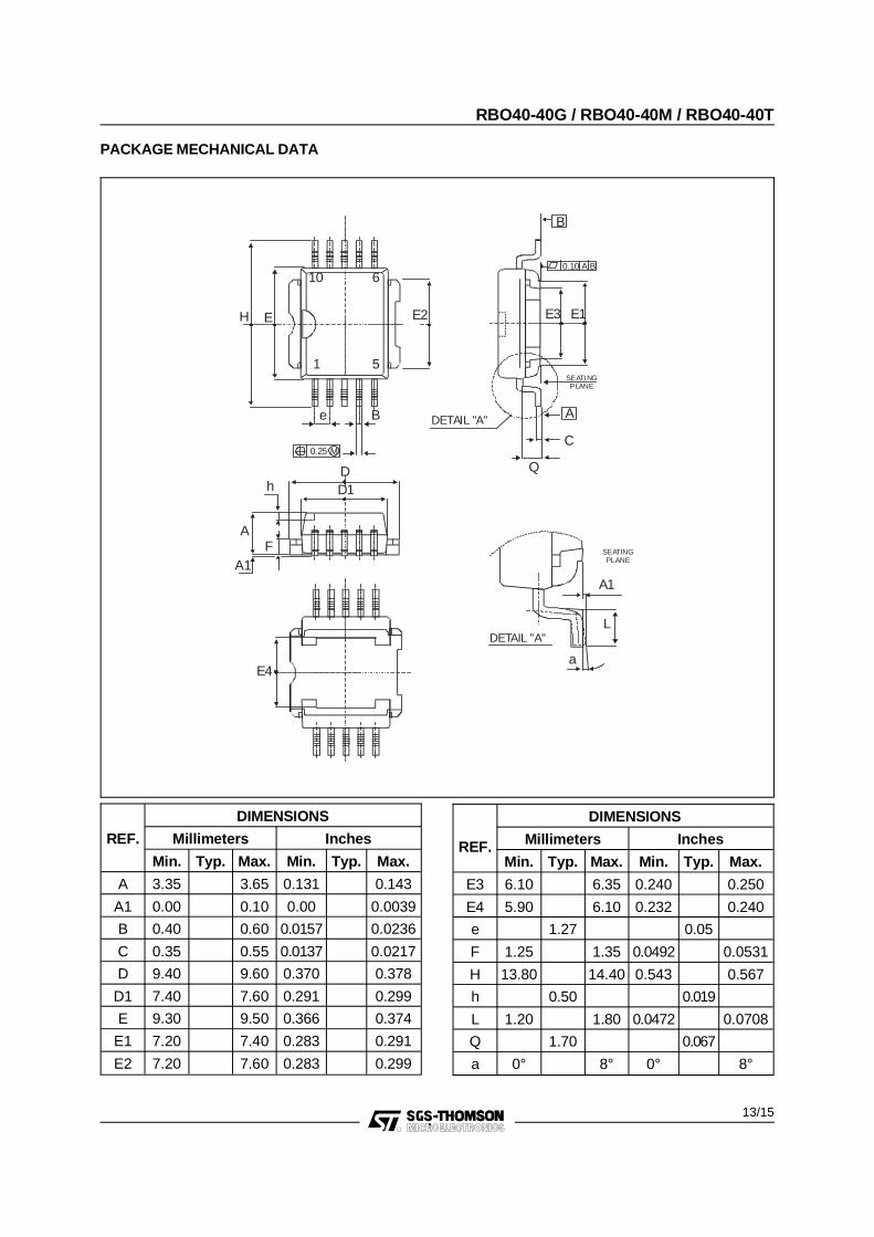
PACKAGE MECHANICAL DATA
D2PAK Plastic
A
C2
D
R
2.0 MIN.FLAT ZONE
A2
V2
C
A1
G
L
L3
L2
B
B2
E
REF.
DIMENSIONS
Millimeters Inches
Min. Typ. Max. Min. Typ. Max.
A 4.30 4.60 0.169 0.181
A1 2.49 2.69 0.098 0.106
A2 0.03 0.23 0.001 0.009
B 0.70 0.93 0.027 0.037
B2 1.40 0.055
C 0.45 0.60 0.017 0.024
C2 1.21 1.36 0.047 0.054
D 8.95 9.35 0.352 0.368
E 10.00 10.28 0.393 0.405
G 4.88 5.28 0.192 0.208
L 15.00 15.85 0.590 0.624
L2 1.27 1.40 0.050 0.055
L3 1.40 1.75 0.055 0.069
R 0.40 0.016
V2 0° 8° 0° 8°
FOOT-PRINT D2PAK
8.903.70
1.30
5.08
16.90
10.30
RBO40-40G / RBO40-40M / RBO40-40T
9/15

SOLDERING RECOMMENDATIONThe soldering process causes considerablethermal stress to a semiconductor component.This has to be minimized to assure a reliable andextended lifetime of the device. The PowerSO-10package can be exposed to a maximumtemperature of 260°C for 10 seconds. However aproper soldering of the package could be done at215°C for 3 seconds. Any solder temperatureprofile should be within these limits. As reflowtechniques are most common in surface mounting,typical heating profiles are given in Figure 1,eitherfor mounting on FR4 or on metal-backed boards.For each particular board, the appropriate heatprofile has to be adjusted experimentally. Thepresent proposal is just a starting point. In anycase, the following precautions have to beconsidered :
- always preheat the device - peak temperature should be at least 30 °C higher than the melting point of the solder alloy chosen
- thermal capacity of the base substrateVoids pose a difficult reliability problem for largesurface mount devices. Such voids under thepackage result in poor thermal contact and thehigh thermal resistance leads to componentfailures. The PowerSO-10 is designed fromscratch to be solely a surface mount package,hence symmetry in the x- and y-axis gives thepackage excellent weight balance. Moreover, thePowerSO-10 offers the unique possibility to controleasily the flatness and quality of the solderingprocess. Both the top and the bottom solderededges of the package are accessible for visualinspection (soldering meniscus).Coplanarity between the substrate and thepackage can be easily verified. The quality of thesolder joints is very important for two reasons : (I)poor quality solder joints result directly in poorreliability and (II) solder thickness affects thethermal resistance significantly. Thus a tightcontrol of this parameter results in thermallyefficient and reliable solder joints.
Fig. 1 : Typical reflow soldering heat profile
Time (s)
Temperature ( C)
0 40 80 120 160 200 240 280 320 3600
50
100
150
200
250
o
215 Co
Soldering
PreheatingCooling
245 Co
Epoxy FR4board
Metal-backedboard
RBO40-40G / RBO40-40M / RBO40-40T
10/15

SUBSTRATES AND MOUNTING INFORMATIONThe use of epoxy FR4 boards is quite common forsurface mounting techniques, however, their poorthermal conduction compromises the otherwiseoutstanding thermal performance of thePowerSO-10. Some methods to overcome thislimitation are discussed below.
One possibility to improve the thermal conductionis the use of large heat spreader areas at thecopper layer of the PC board. This leads to areduction of thermal resistance to 35 °C for 6 cm2
of the board heatsink (see fig. 2).Use of copper-filled through holes on conventionalFR4 techniques will increase the metallization and
decrease thermal resistance accordingly. Usinga configuration with 16 holes under the spreader ofthe package with a pitch of 1.8 mm and a diameterof 0.7 mm, the thermal resistance (junction -heatsink) can be reduced to 12°C/W (see fig. 3).Beside the thermal advantage, this solution allowsmulti-layer boards to be used. However, adrawback of this traditional material prevents itsuse in very high power, high current circuits. Forinstance, it is not advisable to surface mountdevices with currents greater than 10 A on FR4boards. A Power Mosfet or Schottky diode in asurface mount power package can handle up toaround 50 A if better substrates are used.
Fig. 2 : Mounting on epoxy FR4 head dissipation by extending the area of the copper layer
Fig. 3 : Mounting on epoxy FR4 by using copper-filled through holes for heat transfer
FR4 boardCopper foil
FR4 boardCopper foil
heat transferheatsink
RBO40-40G / RBO40-40M / RBO40-40T
11/15

PowerSo-10 package mounted on R th (j-a) P Diss
1.FR4 using the recommended pad-layout 50 °C/W 1.5 W
2.FR4 with heatsink on board (6cm2) 35 °C/W 2.0 W
3.FR4 with copper-filled through holes and external heatsink applied 12 °C/W 5.8 W
4. IMS floating in air (40 cm2) 8 °C/W 8.8 W
5. IMS with external heatsink applied 3.5 °C/W 20 W
TABLE 1
A new technology available today is IMS - anInsulated Metallic Substrate. This offers greatlyenhanced thermal characteristics for surfacemount components. IMS is a substrate consistingof three different layers, (I) the base material whichis available as an aluminium or a copper plate, (II)a thermal conductive dielectrical layer and (III) acopper foil, which can be etched as a circuit layer.Using this material a thermal resistance of 8°C/Wwith 40 cm2 of board floating in air is achievable(see fig. 4). If even higher power is to be dissipatedan external heatsink could be applied which leadsto an Rth(j-a) of 3.5°C/W (see Fig. 5), assumingthat Rth (heatsink-air) is equal to Rth(junction-heatsink). This is commonly applied inpractice, leading to reasonable heatsinkdimensions. Often power devices are defined by
considering the maximum junction temperature ofthe device. In practice , however, this is far frombeing exploited. A summary of various powermanagement capabilities is made in table 1 basedon a reasonable delta T of 70°C junction to air.The PowerSO-10 concept also represents anattractive alternative to C.O.B. techniques.PowerSO-10 offers devices fully tested at lowand high temperature. Mounting is simple - onlyconventional SMT is required - enabling the usersto get rid of bond wire problems and the problem tocontrol the high temperature soft soldering as well.An optimized thermal management is guaranteedthrough PowerSO-10 as the power chips must inany case be mounted on heat spreaders beforebeing mounted onto the substrate.
Fig. 4 : Mounting on metal backed board Fig. 5 : Mounting on metal backed board with anexternal heatsink applied
FR4 boardCopper foil
Aluminium
heatsink
Copper foilInsulation
Aluminium
RBO40-40G / RBO40-40M / RBO40-40T
12/15
PACKAGE MECHANICAL DATA
E2E
1
10
5
6
H
e B
0.25 M
Dh
AF
A1
E4
E3 E1
SEATINGPLANE
SEATINGPLANE
A
B
C
Q
DETAIL "A"
0.10 A B
L
A1
a
DETAIL "A"
D1
REF.
DIMENSIONS
Millimeters Inches
Min. Typ. Max. Min. Typ. Max.
A 3.35 3.65 0.131 0.143
A1 0.00 0.10 0.00 0.0039
B 0.40 0.60 0.0157 0.0236
C 0.35 0.55 0.0137 0.0217
D 9.40 9.60 0.370 0.378
D1 7.40 7.60 0.291 0.299
E 9.30 9.50 0.366 0.374
E1 7.20 7.40 0.283 0.291
E2 7.20 7.60 0.283 0.299
REF.
DIMENSIONS
Millimeters Inches
Min. Typ. Max. Min. Typ. Max.
E3 6.10 6.35 0.240 0.250
E4 5.90 6.10 0.232 0.240
e 1.27 0.05
F 1.25 1.35 0.0492 0.0531
H 13.80 14.40 0.543 0.567
h 0.50 0.019
L 1.20 1.80 0.0472 0.0708
Q 1.70 0.067
a 0° 8° 0° 8°
RBO40-40G / RBO40-40M / RBO40-40T
13/15

HEADER SHAPEFOOT PRINTMOUNTING PAD LAYOUTRECOMMENDED
SHIPPING TUBE
DIMENSIONS (mm)
TYP
ABCLength tube
18120,8532
Quantity per tube 50
Dimensions in millimeters Dimensions in millimeters
Surface mount film taping : contact sales office
B
C
A
RBO40-40G / RBO40-40M / RBO40-40T
14/15

PACKAGE MECHANICAL DATATO220AB Plastic
REF.
DIMENSIONS
Millimeters Inches
Min. Max. Min. Max.
A 14.23 15.87 0.560 0.625
a1 4.50 0.177
a2 12.70 14.70 0.500 0.579
B 10.20 10.45 0.402 0.411
b1 0.64 0.96 0.025 0.038
b2 1.15 1.39 0.045 0.055
C 4.48 4.82 0.176 0.190
c1 0.35 0.65 0.020 0.026
c2 2.10 2.70 0.083 0.106
e 2.29 2.79 0.090 0.110
F 5.85 6.85 0.230 0.270
I 3.55 4.00 0.140 0.157
L 2.54 3.00 0.100 0.118
l2 1.45 1.75 0.057 0.069
l3 0.80 1.20 0.031 0.047
Information furnished is believed to be accurate and reliable. However, SGS-THOMSON Microelectronics assumes no responsibility for theconsequences of use of such information nor for any infringement of patents or other rights of third parties which may result from its use. Nolicense is granted by implication or otherwise under any patent or patent rights of SGS-THOMSON Microelectronics. Specifications mentionedin this publication are subject to change without notice. This publication supersedes and replaces all information previously supplied.SGS-THOMSON Microelectronics products are not authorized for use as critical components in life support devices or systems without expresswritten approval of SGS-THOMSON Microelectronics.
© 1997 SGS-THOMSON Microelectronics - Printed in Italy - All rights reserved.
SGS-THOMSON Microelectronics GROUP OF COMPANIESAustralia - Brazil - Canada - China - France - Germany - Italy - Japan - Korea - Malaysia - Malta - Morocco
The Netherlands - Singapore - Spain - Sweden - Switzerland - Taiwan - Thailand - United Kingdom - U.S.A.
RBO40-40G / RBO40-40M / RBO40-40T
15/15

This datasheet has been download from:
www.datasheetcatalog.com
Datasheets for electronics components.