Features - Future Electronics
16
Device Selection Guide AlGaAs Red HER Orange Yellow Green HDSP-2534 HDSP-2532 HDSP-2530 HDSP-2531 HDSP-2533 Description The HDSP-253x is ideal for applications where displaying eight or more characters of dot matrix information in an aesthetically pleasing manner is required. These devices are eight-digit, 5 x 7 dot matrix, alphanumeric displays. The 5.0 mm (0.2 inch) high characters are packaged in a 0.300 inch (7.62 mm) 30 pin DIP. The on-board CMOS IC has the ability to decode 128 ASCII characters, which are permanently stored in ROM. In addition, 16 pro- grammable symbols may be stored in on-board RAM. Seven brightness levels provide versatility in adjust- ing the display intensity and power consumption. The HDSP-253x is designed for standard micro- processor interface techniques. The display and special features are accessed through a bidirectional eight-bit data bus. Features • XY stackable • 128 character ASCII decoder • Programmable functions • 16 user definable characters • Multi-level dimming and blanking • TTL compatible CMOS IC • Wave solderable Applications • Avionics • Computer peripherals • Industrial instrumentation • Medical equipment • Portable data entry devices • Telecommunications • Test equipment HDSP-253x Series Eight Character 5 mm Smart Alphanumeric Display Data Sheet
Transcript of Features - Future Electronics

Device Selection GuideAlGaAs Red HER Orange Yellow Green
HDSP-2534 HDSP-2532 HDSP-2530 HDSP-2531 HDSP-2533
DescriptionThe HDSP-253x is ideal for applications wheredisplaying eight or more characters of dot matrixinformation in an aesthetically pleasing manner isrequired. These devices are eight-digit, 5 x 7 dotmatrix, alphanumeric displays. The 5.0 mm (0.2 inch)high characters are packaged in a 0.300 inch (7.62mm) 30 pin DIP. The on-board CMOS IC has theability to decode 128 ASCII characters, which arepermanently stored in ROM. In addition, 16 pro-grammable symbols may be stored in on-board RAM.Seven brightness levels provide versatility in adjust-ing the display intensity and power consumption.The HDSP-253x is designed for standard micro-processor interface techniques. The display andspecial features are accessed through a bidirectionaleight-bit data bus.
Features• XY stackable
• 128 character ASCII decoder
• Programmable functions
• 16 user definable characters
• Multi-level dimming and blanking
• TTL compatible CMOS IC
• Wave solderable
Applications• Avionics
• Computer peripherals
• Industrial instrumentation
• Medical equipment
• Portable data entry devices
• Telecommunications
• Test equipment
HDSP-253x SeriesEight Character 5 mm Smart Alphanumeric Display
Data Sheet
2
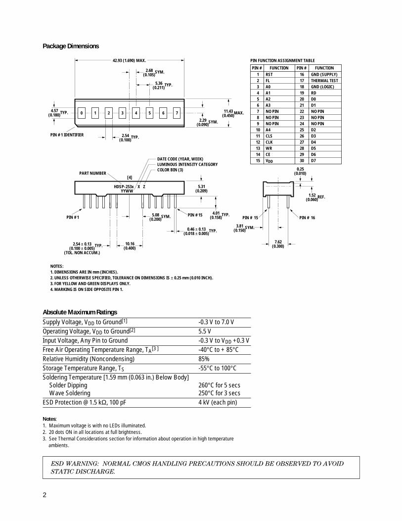
Package Dimensions
Absolute Maximum Ratings
Supply Voltage, VDD to Ground[1] -0.3 V to 7.0 V
Operating Voltage, VDD to Ground[2] 5.5 V
Input Voltage, Any Pin to Ground -0.3 V to VDD +0.3 V
Free Air Operating Temperature Range, TA[3 ] -40°C to + 85°C
Relative Humidity (Noncondensing) 85%
Storage Temperature Range, TS -55°C to 100°C
Soldering Temperature [1.59 mm (0.063 in.) Below Body]Solder Dipping 260°C for 5 secsWave Soldering 250°C for 3 secs
ESD Protection @ 1.5 kΩ, 100 pF 4 kV (each pin)
Notes:1. Maximum voltage is with no LEDs illuminated.2. 20 dots ON in all locations at full brightness.3. See Thermal Considerations section for information about operation in high temperature
ambients.
ESD WARNING: NORMAL CMOS HANDLING PRECAUTIONS SHOULD BE OBSERVED TO AVOIDSTATIC DISCHARGE.
PIN # 15
SYM.
TYP.
DATE CODE (YEAR, WEEK)LUMINOUS INTENSITY CATEGORYCOLOR BIN (3)
3.81(0.150)
PIN # 16
1.52(0.060)
5.31(0.209)
2.29(0.090)
4.57(0.180)
[4]
4.01(0.158)SYM.5.08
(0.200)
10.16(0.400)
TYP.0.46 ± 0.13(0.018 ± 0.005)
TYP.
PIN #1
PART NUMBER
2.54 ± 0.13(0.100 ± 0.005)
(TOL. NON ACCUM.)
7.62(0.300)
REF.
0.25(0.010)
PIN # FUNCTION PIN # FUNCTION
1
2
3
4
5
6
7
8
9
10
11
12
13
14
15
RST
FL
A0
A1
A2
A3
NO PIN
NO PIN
NO PIN
A4
CLS
CLK
WR
CE
VDD
16
17
18
19
20
21
22
23
24
25
26
27
28
29
30
GND (SUPPLY)
THERMAL TEST
GND (LOGIC)
RD
D0
D1
NO PIN
NO PIN
NO PIN
D2
D3
D4
D5
D6
D7
PIN FUNCTION ASSIGNMENT TABLE
3 4 5 6 7
TYP.
SYM.
11.43(0.450)
MAX.TYP.
2.54(0.100)
SYM.2.68(0.105)
42.93 (1.690) MAX.
TYP.5.36(0.211)
PIN #15
PIN #1 IDENTIFIER
NOTES:1. DIMENSIONS ARE IN mm (INCHES).2. UNLESS OTHERWISE SPECIFIED, TOLERANCE ON DIMENSIONS IS ± 0.25 mm (0.010 INCH).3. FOR YELLOW AND GREEN DISPLAYS ONLY.4. MARKING IS ON SIDE OPPOSITE PIN 1.
HDSP-253x X ZYYWW
210

3
ASCII Character Set
Optical Characteristics at 25°C[1]
VDD = 5.0 V at Full Brightness
Luminous Intensity Peak DominantCharacter Average (#) Wavelength Wavelength[2]
IV (mcd) lPEAK (nm) ld (nm) LED Color Part Number Min. Typ. Typ. Typ.
AlGaAs Red HDSP-2534 5.1 25 645 637
High Efficiency Red HDSP-2532 2.5 7.5 635 626
Orange HDSP-2530 2.5 7.5 600 602
Yellow HDSP-2531 2.5 7.5 583 585
Green HDSP-2533 2.5 7.5 568 574
Notes:1. Refers to the initial case temperature of the device immediately prior to measurement.2. Dominant wavelength, ld, is derived from the CIE chromaticity diagram, and represents the single wavelength which defines the color of the device.
D7D6
D5D4BITSD3 D0D2 D1
ROWCOLUMN
0000 0
0001 1
0010 2
0011 3
0100 4
0101 5
0110 6
0111 7
1000 8
1001 9
1010 A
1011 B
1100 C
1101 D
1110 E
1111 F
00
00
0
00
01
1
00
10
2
00
11
3
01
00
4
01
01
5
01
10
6
01
11
7
1X
XX
8–F
16
USER
DEFINED
CHARACTERS

4
Recommended Operating Conditions
Parameter Symbol Minimum Nominal Maximum Units
Supply Voltage VDD 4.5 5.0 5.5 V
Electrical Characteristics over Operating Temperature Range4.5 < VDD < 5.5 unless otherwise specified
25°C 25°CParameter Symbol Min. Typ.[1] Max.[1] Max. Units Test Conditions
Input Leakage II -1.0 1.0 mA VIN = 0 to VDD, Pins CLK,(Input without Pull-up) D0-D7, A0-A4
Input Current IIP -30 -11 -18 0 mA VIN = 0 to VDD, Pins CLS,(Input with Pull-up) RST, WR, RD, CE, FL
IDD Blank IDD(BL) 0.5 3.0 4.0 mA VIN = VDD
IDD 8 Digits 12 Dots/Char[2,3,4] IDD(V) 230 295 390 mA "V" On in All 8 Locations(AlGaAs)
IDD 8 Digits 20 Dots/Char[2,3,4] IDD(#) 330 410 480 mA "#" On in All 8 Locations(AlGaAs)
IDD 8 Digits 12 Dots/Char[2,3,4] IDD(V) 200 255 330 mA "V" On in All 8 Locations(All Colors Except AlGaAs)
IDD 8 Digits 20 Dots/Char[2,3,4] IDD(#) 300 370 430 mA "#" On in All 8 Locations(All Colors Except AlGaAs)
Input Voltage High VIH 2.0 VDD V+0.3 V
Input Voltage Low VIL GND 0.8 V-0.3 V
Output Voltage High VOH 2.4 V VDD = 4.5 V, IOH = -40 µA
Output Voltage Low D0-D7 VOL 0.4 V VDD = 4.5 V, IOL = 1.6 mA
Output Voltage Low CLK VOL 0.4 V VDD = 4.5 V, IOL = 40 µA
Thermal Resistance IC RqJ-PIN 16 °C/W Measured at Pin 17Junction-to-PIN
Notes:1. VDD = 5.0 V.2. See Thermal Considerations Section for information about operation in high temperature ambients.3. Average IDD measured at full brightness. See Table 2 in Control Word Section for IDD at lower brightness levels. Peak IDD = 28/15 x IDD(#).4. Maximum IDD occurs at -55°C.

5
Symbol Description 25°C Typical Minimum[1] Units
FOSC Oscillator Frequency 57 28 kHz
FRF[5] Display Refresh Rate 256 128 Hz
FFL[6] Character Flash Rate 2 1 Hz
tST[7] Self Test Cycle Time 4.6 9.2 sec
Notes:5. FRF = FOSC/224.6. FFL = FOSC/28,672.7. tST = 262,144/FOSC.
AC Timing Characteristics over Temperature RangeVDD = 4.5 to 5.5 V unless otherwise specified.
ReferenceNumber Symbol Description Min.[1] Units1 tACC Display Access Time
Write 210Read 230 ns
2 tACS Address Setup Time to Chip Enable 10 ns
3 tCE Chip Enable Active Time[2, 3]
Write 140Read 160 ns
4 tACH Address Hold Time to Chip Enable 20 ns
5 tCER Chip Enable Recovery Time 60 ns
6 tCES Chip Enable Active Prior to Rising Edge of[2, 3]
Write 140Read 160 ns
7 tCEH Chip Enable Hold Time to Rising Edge of Read/Write Signal[2,3] 0 ns
8 tW Write Active Time 100 ns
9 tWD Data Valid Prior to Rising Edge of Write Signal 50 ns
10 tDH Data Write Hold Time 20 ns
11 tR Chip Enable Active Prior to Valid Data 160 ns
12 tRD Read Active Prior to Valid Data 75 ns
13 tDF Read Data Float Delay 10 ns
tRC Reset Active Time[4] 300 ns
Notes:1. Worst case values occur at an IC junction temperature of 125°C.2. For designers who do not need to read from the display, the Read line can be tied to VDD and the Write and Chip Enable lines can be tied together.3. Changing the logic levels of the Address lines when CE = "0" may cause erroneous data to be entered into the Character RAM, regardless of the
logic levels of the WR and RD lines.4. The display must not be accessed until after 3 clock pulses (110 µs min. using the internal refresh clock) after the rising edge of the reset line.

6
Write Cycle Timing Diagram
Read Cycle Timing Diagram
1
9
8
6
32
CE
7
10
4 2
5
A0 -A4
FL
D0 -D7
WR
INPUT PULSE LEVELS: 0.6 V to 2.4 V
1
12
11
6
3
2
CE
7
13
4 2
5
A0 -A4
FL
D0 -D7
RD
INPUT PULSE LEVELS: 0.6 V to 2.4 VOUTPUT REFERENCE LEVELS: 0.6 V to 2.2 VOUTPUT LOADING = 1 TTL LOAD AND 100 pF

7
Electrical DescriptionPin Function Description
RESET (RST, pin 1) Reset initializes the display.
FLASH (FL, pin 2) FL low indicates an access to the Flash RAM and is unaffected by the state of addresslines A
3-A
4.
ADDRESS INPUTS Each location in memory has a distinct address. Address inputs (A0-A2) select a specific(A0-A4, pins 3-6, 10) location in the Character RAM, the Flash RAM or a particular row in the UDC
(User-Defined Character) RAM. A3-A4 are used to select which section of memory isaccessed. Table 1 shows the logic levels needed to access each section of memory.
Table 1. Logic Levels to Access MemoryFL A4 A3 Section of Memory A2 A1 A00 X X Flash RAM Character Address1 0 0 UDC Address Register Don’t Care1 0 1 UDC RAM Row Address1 1 0 Control Word Register Don’t Care1 1 1 Character RAM Character Address
CLOCK SELECT (CLS, pin 11) This input is used to select either an internal (CLS = 1) or external (CLS = 0) clock source.
CLOCK INPUT/OUTPUT Outputs the master clock (CLS = 1) or inputs a clock (CLS = 0) for slave displays.(CLK, pin 12)
WRITE (WR, pin 13) Data is written into the display when the WR input is low and the CE input is low.
CHIP ENABLE (CE, pin 14) This input must be at a logic low to read or write data to the display and must go highbetween each read and write cycle.
READ (RD, pin 19) Data is read from the display when the RD input is low and the CEinput is low.
DATA Bus The Data bus is used to read from or write to the display.(D0-D7, pins 20, 21, 25-30)
GND (SUPPLY) (pin 16) This is the analog ground for the LED drivers.
GND (LOGIC) (pin 18) This is the digital ground for internal logic.
VDD (POWER) (pin 15) This is the positive power supply input.
Thermal Test (pin 17) This pin is used to measure the IC junction temperature. Do not connect.

8
Figu
re 1
. HD
SP
-253
X in
t ern
al b
lock
dia
gram
.
A3
A4 FL
ENUD
C A
DD
R R
EGIS
TER
UD
CA
DD
R
RD
WR
D0-
D7
CLR
PRE
SET
CE
A3
A4
A0-
A2
D0-
D7 FL CE
WR
RD
A3
A4 FL CE FL CE
A3
A4 FL CE
A3
A4 FL CE
EN8
x 8
CH
AR
AC
TER
RA
MD
0-D
6R
DW
RD
0-D
7A
0-A
2R
ESET
CH
AR
AD
DR
D7
EN
FLA
SHR
AM
FLA
SHD
ATA
RD
WR
D0
A0-
A2
RES
ETC
HA
R A
DD
R
EN
UD
C R
AM D
OT
DA
TA
RD
WR
D0-
D4
D0-
D4
A0-
A2
UD
C A
DD
RR
OW
SET
EN EN RO
WSE
LSE
LFTE
STDEC
OD
ER(*
)
DO
TD
ATA
D0-
D6
TIM
ING
TIM
ING
DO
TD
RIV
ERS
DO
TD
ATA
EN
FLA
SH
CO
NTR
OL
WO
RD
REG
ISTE
R0 1
RD
WR
RST
CLK
OC
S
CLS
CLR
1
CLR
2
D0-
D7
RES
ET
SELF
TES
TR
ESU
LT
2 3 4 6 7
SELF
TEST
IN
SELF
TES
T
SELF
TES
TSE
LFTE
STST
AR
T
8 5
x7LE
DC
HA
RA
CTE
RS
RO
W D
RIV
ERS
VISU
AL
TEST
RO
MTE
ST
CLR
TEST
OK
TEST
OK
INTE
NSI
TY
INTE
NSI
TY
FLA
SHFLA
SH
BLI
NK
BLI
NK
RES
ET
RES
ET
CLO
CK
TIM
ING
AN
DC
ON
TRO
L
CH
AR
AD
DR
RO
W S
ET
TIM
ING
9
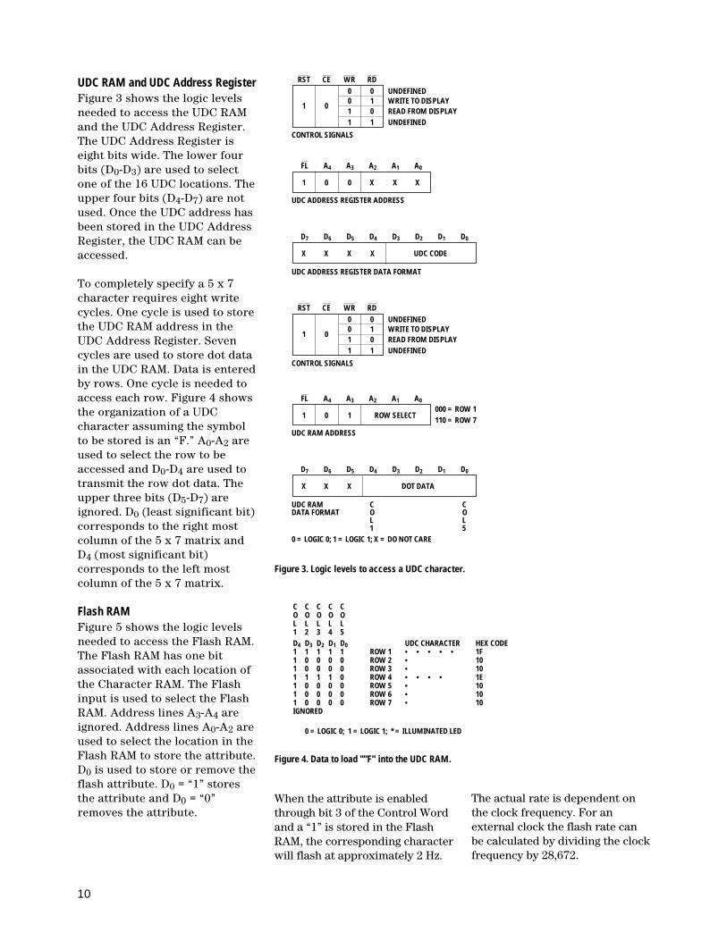
Character RAM This RAM stores either ASCII character data or a UDC RAMaddress.
Flash RAM This is a 1 x 8 RAM which stores Flash data.
User-Defined Character RAM This RAM stores the dot pattern for custom characters.(UDC RAM)
User-Defined Character This register is used to provide the address to the UDC RAM whenAddress Register the user is writing or reading a custom character.(UDC Address Register)
Control Word Register This register allows the user to adjust the display brightness, flashindividual characters, blink, self test or clear the display.
driving of eight 5 x 7 dot matrixcharacters. The major useraccessible portions of thedisplay are listed below:
ASCII decoder, a 16 characterUDC RAM, a UDC AddressRegister, a Control WordRegister and the refreshcircuitry necessary tosynchronize the decoding and
Display Internal Block DiagramFigure 1 shows the internalblock diagram of the HDSP-253Xdisplay. The CMOS IC consists ofan 8 byte Character RAM, an 8bit Flash RAM, a 128 character
Figure 2. Logic levels to access the character RAM.
Character RamFigure 2 shows the logic levelsneeded to access the HDSP-253XCharacter RAM. During a normalaccess the CE = “0” and eitherRD = “0” or WR = “0”. However,erroneous data may be writteninto the Character RAM if theAddress lines are unstable whenCE = “0” regardless of the logiclevels of the RD or WR lines.Address lines A0-A2 are used toselect the location in the Charac-ter RAM. Two types of data canbe stored in each CharacterRAM location: an ASCII code ora UDC RAM address. Data bit D7is used to differentiate betweenthe ASCII character and a UDCRAM address. D7 = 0 enables theASCII decoder and D7 = 1enables the UDC RAM. D0-D6 areused to input ASCII data and D0-D3 are used to input a UDCaddress.
CE
FL A4 A3 A2 A1 A0
RST WR RD
CHARACTERADDRESS
SYMBOL IS ACCESSED IN LOCATIONSPECIFIED BY THE CHARACTER ADDRESS ABOVE
01
0 00 11
1 11
0
1 1
UNDEFINED
CONTROL SIGNALS
CHARACTER RAM ADDRESS
CHARACTER RAM DATA FORMAT
WRITE TO DISPLAYREAD FROM DISPLAY
UNDEFINED
000 = LEFT MOST
111 = RIGHT MOST
D7 D6 D5 D4 D3 D2 D1 D0
0 128 ASCII CODE
X X X UDC CODE1
DISPLAY0 = LOGIC 0; 1 = LOGIC 1; X = DO NOT CARE
DIG0 DIG1 DIG2 DIG3 DIG4 DIG5 DIG6 DIG7
001 010 011 100 101 110 111000
10
UDC RAM and UDC Address RegisterFigure 3 shows the logic levelsneeded to access the UDC RAMand the UDC Address Register.The UDC Address Register iseight bits wide. The lower fourbits (D0-D3) are used to selectone of the 16 UDC locations. Theupper four bits (D4-D7) are notused. Once the UDC address hasbeen stored in the UDC AddressRegister, the UDC RAM can beaccessed.
To completely specify a 5 x 7character requires eight writecycles. One cycle is used to storethe UDC RAM address in theUDC Address Register. Sevencycles are used to store dot datain the UDC RAM. Data is enteredby rows. One cycle is needed toaccess each row. Figure 4 showsthe organization of a UDCcharacter assuming the symbolto be stored is an “F.” A0-A2 areused to select the row to beaccessed and D0-D4 are used totransmit the row dot data. Theupper three bits (D5-D7) areignored. D0 (least significant bit)corresponds to the right mostcolumn of the 5 x 7 matrix andD4 (most significant bit)corresponds to the left mostcolumn of the 5 x 7 matrix.
Flash RAMFigure 5 shows the logic levelsneeded to access the Flash RAM.The Flash RAM has one bitassociated with each location ofthe Character RAM. The Flashinput is used to select the FlashRAM. Address lines A3-A4 areignored. Address lines A0-A2 areused to select the location in theFlash RAM to store the attribute.D0 is used to store or remove theflash attribute. D0 = “1” storesthe attribute and D0 = “0”removes the attribute.
When the attribute is enabledthrough bit 3 of the Control Wordand a “1” is stored in the FlashRAM, the corresponding characterwill flash at approximately 2 Hz.
The actual rate is dependent onthe clock frequency. For anexternal clock the flash rate canbe calculated by dividing the clockfrequency by 28,672.
Figure 3. Logic levels to access a UDC character.
Figure 4. Data to load ""F'' into the UDC RAM.
CE
FL A4 A3 A2 A1 A0
RST WR RD
01
0 00 11
0 01 X X X
0
1 1
UNDEFINED
CONTROL SIGNALS
UDC ADDRESS REGISTER ADDRESS
UDC ADDRESS REGISTER DATA FORMAT
WRITE TO DISPLAYREAD FROM DISPLAY
UNDEFINED
000 = ROW 1
110 = ROW 7
D7 D6 D5 D4 D3 D2 D1 D0
X UDC CODEX X X
FL A4 A3 A2 A1 A0
0 11 ROW SELECT
UDC RAM ADDRESS
UDC RAM C CDATA FORMAT O O
L L1 5
0 = LOGIC 0; 1 = LOGIC 1; X = DO NOT CARE
D7 D6 D5 D4 D3 D2 D1 D0
X DOT DATAX X
CERST WR RD
01
0 00 11 0
1 1
UNDEFINED
CONTROL SIGNALS
WRITE TO DISPLAYREAD FROM DISPLAY
UNDEFINED
C C C C CO O O O OL L L L L1 2 3 4 5
D4 D3 D2 D1 D0 UDC CHARACTER HEX CODE1 1 1 1 1 ROW 1 • • • • • 1F1 0 0 0 0 ROW 2 • 101 0 0 0 0 ROW 3 • 101 1 1 1 0 ROW 4 • • • • 1E1 0 0 0 0 ROW 5 • 101 0 0 0 0 ROW 6 • 101 0 0 0 0 ROW 7 • 10IGNORED
0 = LOGIC 0; 1 = LOGIC 1; * = ILLUMINATED LED

11
Table 2. Current Requirements at Different Brightness Levels for All ColorsExcept AlGaAs
% VDD = 5.0 VSymbol D2 D1 D0 Brightness 25°C Typ. UnitsIDD (V) 0 0 0 100 200 mA
0 0 1 80 160 mA0 1 0 53 106 mA0 1 1 40 80 mA1 0 0 27 54 mA1 0 1 20 40 mA1 1 0 13 26 mA
Figure 5. Logic levels to access the Flash RAM.
Control Word RegisterFigure 6 shows how to access theControl Word Register. This is aneight bit register which performsfive functions. They areBrightness control, Flash RAMcontrol, Blinking, Self Test andClear. Each function isindependent of the others. How-ever, all bits are updated duringeach Control Word write cycle.
Brightness (Bits 0-2)Bits 0-2 of the Control Wordadjust the brightness of thedisplay. Bits 0-2 are interpretedas a three bit binary code withcode (000) corresponding tomaximum brightness and code(111) corresponding to a blankeddisplay. In addition to varying thedisplay brightness, bits 0-2 alsovary the average value of IDD. IDDcan be calculated at anybrightness level by multiplying thepercent brightness level by thevalue of IDD at the 100%brightness level. These values ofIDD are shown in Table 2.
Flash Function (Bit 3)Bit 3 determines whether theflashing character attribute is onor off. When bit 3 is a “1,” theoutput of the Flash RAM ischecked. If the content of a loca-tion in the Flash RAM is a “1,” the
associated digit will flash atapproximately 2 Hz. For anexternal clock, the blink rate canbe calculated by dividing the clockfrequency by 28,672. If the flashenable bit of the Control Word is a“0,” the content of the Flash RAMis ignored. To use this functionwith multiple display systems seethe Reset section.
Blink Function (Bit 4)Bit 4 of the Control Word is usedto synchronize blinking of all eight
digits of the display. When this bitis a “1” all eight digits of thedisplay will blink at approxi-mately 2 Hz. The actual rate isdependent on the clock frequency.For an external clock, the blinkrate can be calculated by dividingthe clock frequency by 28,672.This function will override theFlash function when it is active.To use this function with multipledisplay systems see the Resetsection.
Figure 6. Logic levels to access the control word register.
CE
FL A4 A3 A2 A1 A0
RST WR RD
01
0 00 11
X X0
0
1 1
UNDEFINED
REMOVE FLASH ATSPECIFIED DIGIT LOCATIONSTORE FLASH ATSPECIFIED DIGIT LOCATION
CONTROL SIGNALS
FLASH RAM ADDRESS
FLASH RAM DATA FORMAT
0 = LOGIC 0; 1 = LOGIC 1; X = DO NOT CARE
WRITE TO DISPLAYREAD FROM DISPLAY
UNDEFINED
D7 D6 D5 D4 D3 D2 D1 D0
X X X X X X X01
CHARACTERADDRESS
000 = LEFT MOST
111 = RIGHT MOST
CE
FL A4 A3 A2 A1 A0
RST WR RD
01
0 00 11
1 0 X X X1
0
1 1
UNDEFINED
CONTROL SIGNALS
CONTROL WORD ADDRESS
CONTROL WORD DATA FORMAT
0 = LOGIC 0; 1 = LOGIC 1; X = DO NOT CARE
0 DISABLE FLASH1 ENABLE FLASH
BRIGHTNESSCONTROLLEVELS
0 DISABLE BLINKING1 ENABLE BLINKING
0 NORMAL OPERATION1 CLEAR FLASH AND CHARACTER RAMS
0 X NORMAL OPERATION; X IS IGNORED1 X START SELF TEST; RESULT GIVEN IN X X = 0 FAILED X = 1 PASSED
WRITE TO DISPLAYREAD FROM DISPLAY
UNDEFINED
D7 D6 D5 D4 D3 D2 D1 D0
C S S BL F B
0 0 0 100%0 0 1 80%0 1 0 53%0 1 1 40%1 0 0 27%1 0 1 20%1 1 0 13%1 1 1 0%
B B

12
Self Test Function (Bits 5, 6)Bit 6 of the Control Word Regis-ter is used to initiate the self testfunction. Results of the internalself test are stored in bit 5 of theControl Word. Bit 5 is a readonly bit where bit 5 = “1”indicates a passed self test andbit 5 = “0” indicates a failed selftest.
Setting bit 6 to a logic 1 willstart the self test function. Thebuilt-in self test function of theIC consists of two internal rou-tines which exercises majorportions of the IC and illumin-ates all of the LEDs. The firstroutine cycles the ASCII decoderROM through all states andperforms a checksum on theoutput. If the checksum agreeswith the correct value, bit 5 isset to “1.” The second routineprovides a visual test of theLEDs using the drive circuitry.This is accomplished by writingcheckered and inversecheckered patterns to thedisplay. Each pattern isdisplayed for approximately 2seconds.
During the self test function thedisplay must not be accessed.The time needed to execute theself test function is calculated bymultiplying the clock period by262,144. For example, assume aclock frequency of 58 KHz, thenthe time to execute the self testfunction frequency is equal to(262,144/58,000) = 4.5 secondduration.
At the end of the self test func-tion, the Character RAM isloaded with blanks, the ControlWord Register is set to zeros
except for bit 5, and the FlashRAM is cleared and the UDCAddress Register is set to allones.
Clear Function (Bit 7)Bit 7 of the Control Word willclear the Character RAM and theFlash RAM. Setting bit 7 to a “1”will start the clear function.Three clock cycles (110 ms min.using the internal refresh clock)are required to complete theclear function. The display mustnot be accessed while thedisplay is being cleared. Whenthe clear function has been com-pleted, bit 7 will be reset to a“0.” The ASCII character codefor a space (20H) will be loadedinto the Character RAM to blankthe display and the Flash RAMwill be loaded with “1”s. TheUDC RAM, UDC AddressRegister and the remainder ofthe Control Word are unaffected.
Display ResetFigure 7 shows the logic levelsneeded to reset the display. Thedisplay should be reset onPower-up. The external Resetclears the Character RAM, FlashRAM, Control Word and resetsthe internal counters. After therising edge of the Reset signal,three clock cycles (110 ms min.using the internal refresh clock)
are required to complete thereset sequence. The display mustnot be accessed while thedisplay is being reset. The ASCIICharacter code for a space (20H)will be loaded into the CharacterRAM to blank the display. TheFlash RAM and Control WordRegister are loaded with all "0"s.The UDC RAM and UDC AddressRegister are unaffected. Alldisplays which operate with thesame clock source must besimultaneously reset tosynchronize the Flashing andBlinking functions.
Mechanical ConsiderationsThe HDSP-253X is assembled bydie attaching and wire bonding280 LED chips and a CMOS IC toa thermally conductive printedcircuit board. A polycarbonatelens placed over the pcb createsan air gap over the LED wirebonds. A backfill epoxy seals thedisplay package.
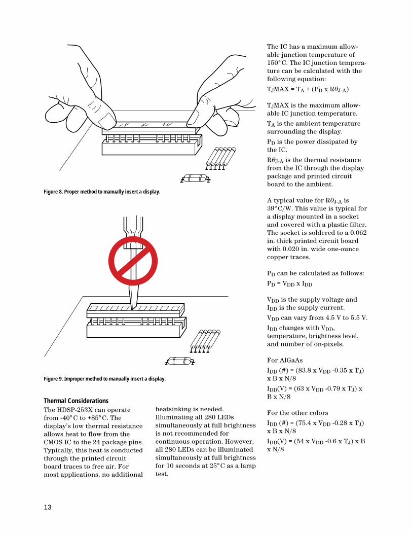
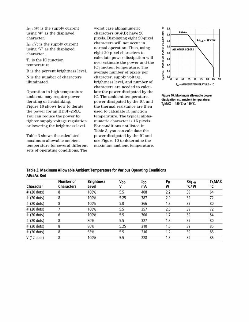
Figure 8 shows the propermethod to insert the display byhand. To prevent damage to theLED wire bonds, apply pressureuniformly with fingers located atboth ends of the part. Using atool, shown in Figure 9, such asa screwdriver or pliers to pushthe display into the printedcircuit board or socket maydamage the LED wire bonds. Theforce exerted by a screwdriver issufficient to push the lens intothe LED wire bonds. The bentwire bonds cause shorts oropens that result in catastrophicfailure of the LEDs.
CERST WR RD
0 = LOGIC 0; 1 = LOGIC 1; X = DO NOT CARE
NOTE:IF RST, CE, AND WR ARE LOW, UNKNOWNDATA MAY BE WRITTEN INTO THE DISPLAY.
FL
0 1 X X X X X
A4 -A0 D7 -D0
Figure 7. Logic levels to reset the display.
13
Figure 9. Improper method to manually insert a display.
Thermal ConsiderationsThe HDSP-253X can operatefrom -40°C to +85°C. Thedisplay’s low thermal resistanceallows heat to flow from theCMOS IC to the 24 package pins.Typically, this heat is conductedthrough the printed circuitboard traces to free air. Formost applications, no additional
heatsinking is needed.Illuminating all 280 LEDssimultaneously at full brightnessis not recommended forcontinuous operation. However,all 280 LEDs can be illuminatedsimultaneously at full brightnessfor 10 seconds at 25°C as a lamptest.
The IC has a maximum allow-able junction temperature of150°C. The IC junction tempera-ture can be calculated with thefollowing equation:
TJMAX = TA + (PD x RqJ-A)
TJMAX is the maximum allow-able IC junction temperature.
TA is the ambient temperaturesurrounding the display.
PD is the power dissipated bythe IC.
RqJ-A is the thermal resistancefrom the IC through the displaypackage and printed circuitboard to the ambient.
A typical value for RqJ-A is39°C/W. This value is typical fora display mounted in a socketand covered with a plastic filter.The socket is soldered to a 0.062in. thick printed circuit boardwith 0.020 in. wide one-ouncecopper traces.
PD can be calculated as follows:
PD = VDD x IDD
VDD is the supply voltage andIDD is the supply current.
VDD can vary from 4.5 V to 5.5 V.
IDD changes with VDD,temperature, brightness level,and number of on-pixels.
For AlGaAs
IDD (#) = (83.8 x VDD -0.35 x TJ)x B x N/8
IDD(V) = (63 x VDD -0.79 x TJ) xB x N/8
For the other colors
IDD (#) = (75.4 x VDD -0.28 x TJ)x B x N/8
IDD(V) = (54 x VDD -0.6 x TJ) x Bx N/8
Figure 8. Proper method to manually insert a display.
IDD (#) is the supply currentusing “#” as the displayedcharacter.
IDD(V) is the supply currentusing “V” as the displayedcharacter.
TJ is the IC junctiontemperature.
B is the percent brightness level.
N is the number of charactersilluminated.
Operation in high temperatureambients may require powerderating or heatsinking.Figure 10 shows how to deratethe power for an HDSP-253X.You can reduce the power bytighter supply voltage regulationor lowering the brightness level.
Table 3 shows the calculatedmaximum allowable ambienttemperature for several differentsets of operating conditions. The
worst case alphanumericcharacters (#,@,B) have 20pixels. Displaying eight 20-pixelcharacters will not occur innormal operation. Thus, usingeight 20-pixel characters tocalculate power dissipation willover estimate the power and theIC junction temperature. Theaverage number of pixels percharacter, supply voltage,brightness level, and number ofcharacters are needed to calcu-late the power dissipated by theIC. The ambient temperature,power dissipated by the IC, andthe thermal resistance are thenused to calculate IC junctiontemperature. The typical alpha-numeric character is 15 pixels.For conditions not listed inTable 3, you can calculate thepower dissipated by the IC anduse Figure 10 to determine themaximum ambient temperature.
Table 3. Maximum Allowable Ambient Temperature for Various Operating ConditionsAlGaAs Red
Number of Brightness VDD IDD PD RqJ-A TAMAXCharacter Characters Level V mA W °C/W °C
# (20 dots) 8 100% 5.5 408 2.2 39 64
# (20 dots) 8 100% 5.25 387 2.0 39 72
# (20 dots) 8 100% 5.0 366 1.8 39 80
# (20 dots) 7 100% 5.5 357 2.0 39 72
# (20 dots) 6 100% 5.5 306 1.7 39 84
# (20 dots) 8 80% 5.5 327 1.8 39 80
# (20 dots) 8 80% 5.25 310 1.6 39 85
# (20 dots) 8 53% 5.5 216 1.2 39 85
V (12 dots) 8 100% 5.5 228 1.3 39 85
Figure 10. Maximum allowable powerdissipation vs. ambient temperature.TJMAX = 150°C or 120°C.
P D M
AX
. – M
AX
IMU
M P
OW
ER D
ISSI
PATI
ON
– W
501.5
TA – AMBIENT TEMPERATURE – °C
8555 60 80 90
2.3
2.2
2.1
1.8
1.7
1.6
70 7565
2.0
1.9
AlGaAs
RqJ-A = 39°C/W
ALL OTHER COLORS
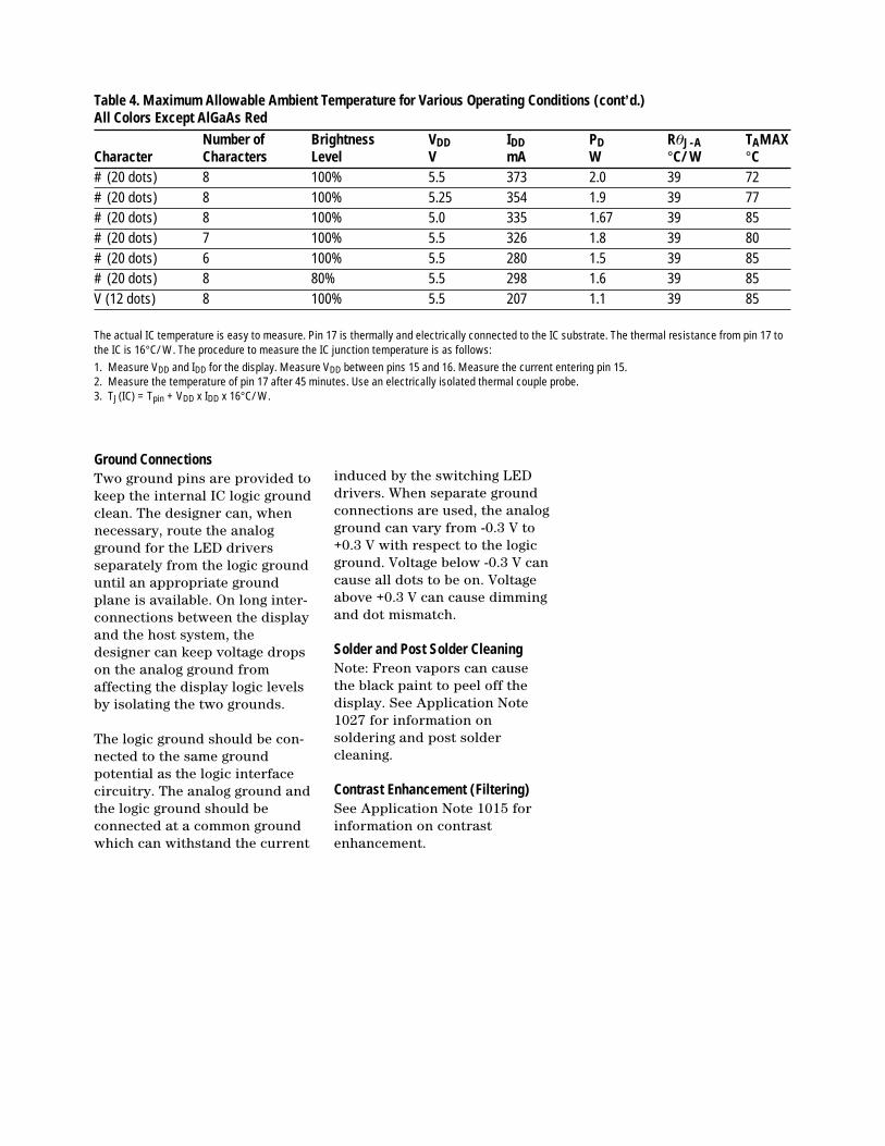
Table 4. Maximum Allowable Ambient Temperature for Various Operating Conditions (cont’d.)All Colors Except AlGaAs Red
Number of Brightness VDD IDD PD RqJ-A TAMAXCharacter Characters Level V mA W °C/W °C
# (20 dots) 8 100% 5.5 373 2.0 39 72
# (20 dots) 8 100% 5.25 354 1.9 39 77
# (20 dots) 8 100% 5.0 335 1.67 39 85
# (20 dots) 7 100% 5.5 326 1.8 39 80
# (20 dots) 6 100% 5.5 280 1.5 39 85
# (20 dots) 8 80% 5.5 298 1.6 39 85
V (12 dots) 8 100% 5.5 207 1.1 39 85
The actual IC temperature is easy to measure. Pin 17 is thermally and electrically connected to the IC substrate. The thermal resistance from pin 17 tothe IC is 16°C/W. The procedure to measure the IC junction temperature is as follows:
1. Measure VDD and IDD for the display. Measure VDD between pins 15 and 16. Measure the current entering pin 15.2. Measure the temperature of pin 17 after 45 minutes. Use an electrically isolated thermal couple probe.3. TJ(IC) = Tpin + VDD x IDD x 16°C/W.
Ground ConnectionsTwo ground pins are provided tokeep the internal IC logic groundclean. The designer can, whennecessary, route the analogground for the LED driversseparately from the logic grounduntil an appropriate groundplane is available. On long inter-connections between the displayand the host system, thedesigner can keep voltage dropson the analog ground fromaffecting the display logic levelsby isolating the two grounds.
The logic ground should be con-nected to the same groundpotential as the logic interfacecircuitry. The analog ground andthe logic ground should beconnected at a common groundwhich can withstand the current
induced by the switching LEDdrivers. When separate groundconnections are used, the analogground can vary from -0.3 V to+0.3 V with respect to the logicground. Voltage below -0.3 V cancause all dots to be on. Voltageabove +0.3 V can cause dimmingand dot mismatch.
Solder and Post Solder CleaningNote: Freon vapors can causethe black paint to peel off thedisplay. See Application Note1027 for information onsoldering and post soldercleaning.
Contrast Enhancement (Filtering)See Application Note 1015 forinformation on contrastenhancement.

Color Bin LimitsColor Range (nm)
Color Bin Min. Max.
Green 1 576.0 580.0
2 573.0 577.0
3 570.0 574.0
4 567.0 571.0
Yellow 3 581.5 585.0
4 584.0 587.5
5 586.5 590.0
6 589.0 592.5
7 591.5 595.0
Note:Test conditions as specified in OpticalCharacteristic table.
Intensity Bin Limits forHDSP-253x
Intensity Range (mcd)Bin Min. Max.
G 2.50 4.00
H 3.41 6.01
I 5.12 9.01
J 7.68 13.52
K 11.52 20.28
Note:Test conditions as specified in OpticalCharacteristic table.
Intensity Bin Limits forHDSP-2534
Intensity Range (mcd)
Bin Min. Max.
I 5.12 9.01
J 7.68 13.52
K 11.52 20.28
L 17.27 30.42
M 25.91 45.63
Note:Test conditions as specified in OpticalCharacteristic table.
For product information and a complete list of distributors, please go to our website: www.avagotech.com
Avago, Avago Technologies, and the A logo are trademarks of Avago Technologies, Pte. in the United States and other countries.Data subject to change. Copyright © 2006 Avago Technologies Pte. All rights reserved. Obsoletes 5988-4669EN5989-3184EN May 9, 2006