
Radiation Performance Data Package MUX8522-S · in a 56 lead High Temperature Co-Fired Ceramic...
56
Prepared by: Aeroflex Plainview, Inc. 35 South Service Road Plainview, NY 11803 March 15, 2010 Radiation Performance Data Package MUX8522-S MUX8522-S DSCC SMD Part Number: 5962-0923101KXC Dual 16 channel analog multiplexer, high impedance analog input.
Transcript of Radiation Performance Data Package MUX8522-S · in a 56 lead High Temperature Co-Fired Ceramic...

Prepared by:
Aeroflex Plainview, Inc. 35 South Service Road Plainview, NY 11803
March 15, 2010
Radiation Performance Data Package
MUX8522-S
MUX8522-S DSCC SMD Part Number: 5962-0923101KXC
Dual 16 channel analog multiplexer, high impedance analog input.

PAGE 2 of 2
1. MUX8522-S:
1.1 Part Description
1.1.1 Dual 16 channel analog multiplexer, high impedance analog input.
1.2 Applicable Documents
1.2.1 Appendix A: Data Sheet: MUX8522 Dual 16-Channel Analog Multiplexer Module, Radiation Tolerant & ESD Protected
1.2.2 Appendix B: DSCC SMD: 5962-95630 RADIATION HARDENED, SINGLE 16
CHANNEL ANALOG MUX DIE
1.2.3 Appendix C: DSCC SMD: 5962-09231 MICROCIRCUIT, HYBRID, LINEAR, DUAL 16 CHANNEL, ANALOG MULTIPLEXER
2. Radiation Performance
2.1 Total Dose: 300 krads(Si), Dose rate = 50 - 300 rads(Si)/s
2.1.1 Per analog multiplexer IC manufacturer's DSCC SMD Specification. 2.1.2 See Appendix B: DSCC SMD: 5962-95630, sheet 4, Section 1.5 Radiation features. 2.1.3 Every wafer lot is subjected to RLAT testing at the stated total dose and dose rate.
2.2 SEU: Immune up to 120 MeV-cm2/mg
2.2.1 Per analog multiplexer IC manufacturer's DSCC SMD Specification 2.2.2 See Appendix B: DSCC SMD: 5962-95630, sheet 4, Section 1.5 Radiation features.
2.3 SEL: Immune, guaranteed by process design
2.3.1 Per analog multiplexer IC manufacturer's DSCC SMD Specification 2.3.2 See Appendix B: DSCC SMD: 5962-95630, sheet 4, Section 1.5 Radiation features. 2.3.3 See Appendix B: DSCC SMD: 5962-95630, sheet 4, note 3/.

SCD8522 Rev A
FEATURESq 32-channels provided by two independent 16-channel multiplexersq Radiation performance
- Total dose: 300 krads(Si), Dose rate = 50 - 300 rads(Si)/s- SEU: Immune up to 120 MeV-cm2/mg- SEL: Immune by process design
q Full military temperature range
q Low power consumption < 30mW
q Separate address (A0-3 & B0-3) and enable (EN0-15 & EN16-31) for CH0-15 and CH16-31
q Fast access time 1500ns typical
q Break-Before-Make switching
q High analog input impedance (power on or off )
q Designed for aerospace and high reliability space applicationsq Packaging – Hermetic ceramic
- 56 leads, 0.80"Sq x 0.20"Ht quad flat pack - Typical Weight 6 grams
q DSCC SMD 5962-09231 pending
MUX8522 Dual 16-Channel Analog Multiplexer ModuleRadiation Tolerant
GENERAL DESCRIPTIONAeroflex’s MUX8522 is a radiation tolerant, dual 16 channel multiplexer MCM (Multi Chip Module).The MUX8522 has been specifically designed to meet exposure to radiation environments. It is availablein a 56 lead High Temperature Co-Fired Ceramic (HTCC) Quad Flatpack (CQFP). It is guaranteedoperational from -55°C to +125°C. Available screened in accordance with MIL-PRF-38534, theMUX8522 is ideal for demanding military and space applications.
ORGANIZATION AND APPLICATIONThe MUX8522 consists of two independent 16 channel multiplexers arranged as shown in the blockdiagram.
A SectionSixteen (16) channels addressable by bus A0~A3, enabled by EN0-15 and outputted on Output1(0-15).
B SectionSixteen (16) channels addressable by bus B0~B3, enabled by EN16-31 and outputted on Output2(16-31).
Standard Products
April 17, 2009
Note: Aeroflex Plainview does not currently have a DSCC certified Radiation Hardened Assurance Program.
www.aeroflex.com/mux
rbenson
Highlight

2SCD8522 Rev A 4/17/09 Aeroflex Plainview
MUX8522: DUAL 16 CHANNEL ANALOG MUX BLOCK DIAGRAM
CH 0
CH 15•
••
EN 0-15
OUTPUT2 (16-31)
B0B1B2B3
OUTPUT1 (0-15)MUX 1
MUX 2
16
-VEE VREF
GND
CH 16
CH 31•
••
16
EN 16-31
A0A1A2A3
+VEE
SECTION A
SECTION B

3SCD8522 Rev A 4/17/09 Aeroflex Plainview
ABSOLUTE MAXIMUM RATINGS 1/
Parameter Range Units
Case Operating Temperature Range -55 to +125 °C
Storage Temperature Range -65 to +150 °C
Supply Voltage+VEE (Pin 18) -VEE (Pin 46) VREF (Pin 39)
+16.5-16.5+16.5
VVV
Digital Input OvervoltageVEN0-15 (Pin 13), VEN16-31 (Pin 44), VA (Pins 14, 15, 16, 17), VB (Pins 40, 41, 42, 43)
< VREF +4> GND -4
VV
Analog Input Over VoltageVS ±35V V
Notes: 1/ All measurements are made with respect to ground.
NOTICE: Stresses above those listed under "Absolute Maximums Rating" may cause permanent damage to the device. These are stress rating only; functional operation beyond the "Operation Conditions" is not recommended and extended exposure beyond the "Operation Conditions" may affect device reliability.
RECOMMENDED OPERATING CONDITIONS 1/
Symbol Parameter Typical Units
+VEE +15V Power Supply Voltage +15.0 V
-VEE -15V Power Supply Voltage -15.0 V
VREF Reference Voltage +5.00 V
VAL Logic Low Level +0.8 V
VAH Logic High Level +4.0 V
1/ Power Supply turn-on sequence shall be as follows: +VEE, -VEE, followed by VREF.
DC ELECTRICAL PERFORMANCE CHARACTERISTICS 1/ (TC = -55°C TO +125°C, +VEE = +15V, -VEE = -15V, VREF = +5.0V - UNLESS OTHERWISE SPECIFIED)
Parameter Symbol Conditions Min Max Units
Supply Current +IEE VEN(0-15) = VEN(16-31) = VA(0-3) = VB(0-3) = 0 0.1 1 mA
-IEE VEN(0-15) = VEN(16-31) = VA(0-3) = VB(0-3) = 0 -1 -0.1 mA
+ISBY VEN(0-15) = VEN(16-31) = 4V, VA(0-3) = VB(0-3) = 0 6/ 0.1 1 mA
-ISBY VEN(0-15) = VEN(16-31) = 4V, VA(0-3) = VB(0-3) = 0 6/ -1 -0.1 mA
Address Input Current IAL(0-3)A VA = 0V -1 1 µA
IAH(0-3)A VA = 5V -1 1 µA
IAL(0-3)B VB = 0V -1 1 µA
IAH(0-3)B VB = 5V -1 1 µA
Enable Input Current IENL(0-15) VEN(0-15) = 0V -1 1 µA
IENH(0-15) VEN(0-15) = 5V -1 1 µA
IENL(16-31) VEN(16-31) = 0V -1 1 µA
IENH(16-31) VEN(16-31) = 5V -1 1 µA

4SCD8522 Rev A 4/17/09 Aeroflex Plainview
Positive Input Leakage Current CH0-CH31 +ISOFFOUTPUT(ALL) VIN = +10V, VEN = 4V, output and all unused MUX inputs
under test = -10V 2/, 3/ -100 +100 nA
Negative Input Leakage Current CH0-CH31 -ISOFFOUTPUT(ALL) VIN = -10V, VEN = 4V, output and all unused MUX inputs
under test = +10V 2/, 3/ -100 +100 nA
Positive Output Leakage Current OUTPUTS (pins 12,45)
+IDOFFOUTPUT(ALL) VOUT = +10V, VEN = 4V, output and all unused MUX inputs under test = -10V 3/, 4/ -100 +100 nA
Negative Output Leakage Current OUTPUTS (pins 12,45)
-IDOFFOUTPUT(ALL) VOUT = -10V, VEN = 4V, output and all unused MUX inputs under test = +10V 3/, 4/ -100 +100 nA
Switch ON Resistance OUTPUTS (pins 12,45)
RDS(ON)(0-31)A VIN = +15V, VEN = 0.8V, IOUT = -1mA 2/, 3/, 5/ 500 3000 Ω
RDS(ON)(0-31)B VIN = +5V, VEN = 0.8V, IOUT = -1mA 2/, 3/, 5/ 500 3000 Ω
RDS(ON)(0-31)C VIN = -5V, VEN = 0.8V, IOUT = +1mA 2/, 3/, 5/ 500 3000 Ω
Notes:1/ Measure inputs sequentially. Ground all unused inputs of the device under test. VA is the applied input voltage to the address lines A(0-3). VB is
the applied input voltage to the address lines B(0-3).2/ VIN is the applied input voltage to the input channels CH0-CH31.3/ VEN 0-15 is the applied input voltage to the enable line EN (0-15). VEN 16-31 is the applied input voltage to the enable line EN (16-31)4/ VOUT is the applied input voltage to the output lines OUTPUT1 (0-15), OUTPUT2 (16-31)5/ Negative current is the current flowing out of each of the MUX pins. Positive current is the current flowing into each MUX pin.6/ Not tested, guaranteed to the specified limits.
SWITCHING CHARACTERISTICS (TC = -55°C TO +125°C, +VEE = +15V, -VEE = -15V, VREF = +5.0V -- UNLESS OTHERWISE SPECIFIED)
Parameter Symbol Conditions Min Max Units
Switching Test MUX tAHL RL = 10KΩ, CL = 50pF 10 1500 ns
tALHRL = 10KΩ, CL = 50pF Tc = +25°C, +125°C Tc = -55°C
1010
20005000
nsns
tONENRL = 1KΩ, CL = 50pF
10 1500 ns
tOFFEN 10 1000 ns
DC ELECTRICAL PERFORMANCE CHARACTERISTICS 1/ (continued)(TC = -55°C TO +125°C, +VEE = +15V, -VEE = -15V, VREF = +5.0V - UNLESS OTHERWISE SPECIFIED)
Parameter Symbol Conditions Min Max Units

5SCD8522 Rev A 4/17/09 Aeroflex Plainview
TRUTH TABLE (CH0 – CH15)
A3 A2 A1 A0 EN (0-15) "ON" CHANNEL, 1/ (OUTPUT 1)
X X X X H NONE
L L L L L CH0
L L L H L CH1
L L H L L CH2
L L H H L CH3
L H L L L CH4
L H L H L CH5
L H H L L CH6
L H H H L CH7
H L L L L CH8
H L L H L CH9
H L H L L CH10
H L H H L CH11
H H L L L CH12
H H L H L CH13
H H H L L CH14
H H H H L CH15
1/ Between CH0-15 and OUTPUT1 (0-15)
TRUTH TABLE (CH16 – CH31)
B3 B2 B1 B0 EN (16-31) "ON" CHANNEL, 1/ (OUTPUT 2)
X X X X H NONE
L L L L L CH16
L L L H L CH17
L L H L L CH18
L L H H L CH19
L H L L L CH20
L H L H L CH21
L H H L L CH22
L H H H L CH23
H L L L L CH24
H L L H L CH25
H L H L L CH26
H L H H L CH27
H H L L L CH28
H H L H L CH29
H H H L L CH30
H H H H L CH31
1/ Between CH16-31 and OUTPUT2 (16-31)

6SCD8522 Rev A 4/17/09 Aeroflex Plainview
MUX8522 SWITCHING DIAGRAMS
4.0V
50%
~3V to 10.0V
50%
0V
tOFFENtONEN
Definition of tONEN and tOFFEN
0.8V
0V
0V
50%
50%
4.0V
0.8V
50%
11.6V MIN
11.6V MIN
4.0VAddress Lines
tAHL
50%
NOTE: f = 10KHz, Duty cycle = 50%.
(A0 - A3 /B0 - B3)
MUX Output
MUX Output
MUX Output
Address Lines(A0 - A3 /B0 - B3)
EN Lines
tALH
Definition of tAHL
Definition of tALH
0.8V

7SCD8522 Rev A 4/17/09 Aeroflex Plainview
Notes: 1. It is recommended that all "NC" or "no connect pin", be grounded. This eliminates or minimizes any ESD or static buildup. 2. Package lid is internally connected to circuit ground (Pins 7, 8, 11, 21, 22, 35, 36, 49, 50).
PIN NUMBERS & FUNCTIONS
MUX8522 – 56 Leads Ceramic QUAD Flat Pack
Pin # Function Pin # Function
1 CH0 29 CH31
2 CH1 30 CH30
3 CH2 31 CH29
4 CH3 32 CH28
5 CH4 33 CH27
6 CH5 34 CH26
7 GND 35 GND
8 GND 36 GND
9 CH6 37 CH25
10 CH7 38 CH24
11 CASE GND 39 VREF
12 OUTPUT1 (0-15) 40 B3
13 EN 0-15 41 B2
14 A0 42 B1
15 A1 43 B0
16 A2 44 EN 16-31
17 A3 45 OUTPUT2 (16-31)
18 +VEE 46 -VEE
19 CH15 47 CH16
20 CH14 48 CH17
21 GND 49 GND
22 GND 50 GND
23 CH13 51 CH18
24 CH12 52 CH19
25 CH11 53 CH20
26 CH10 54 CH21
27 CH9 55 CH22
28 CH8 56 CH23

SCD8522 Rev A 4/17/09 8
PLAINVIEW, NEW YORKToll Free: 800-THE-1553 Fax: 516-694-6715
SE AND MID-ATLANTIC Tel: 321-951-4164 Fax: 321-951-4254
INTERNATIONALTel: 805-778-9229Fax: 805-778-1980
WEST COAST Tel: 949-362-2260Fax: 949-362-2266
NORTHEASTTel: 603-888-3975Fax: 603-888-4585
CENTRALTel: 719-594-8017Fax: 719-594-8468
w w w . a e r o f l e x . c o m i n f o - a m s @ a e r o f l e x . c o m
Aeroflex Microelectronic Solutions reserves the right to change at any time without notice the specifications, design, function, or form of its products described herein. All parameters must be validated for each customer's application by engineering. No liability is assumed as a result of use of this product. No patent licenses are implied.
Our passion for performance is defined by threeattributes represented by these three icons:solution-minded, performance-driven and customer-focused
EXPORT CONTROL: EXPORT WARNING:This product is controlled for export under the International Traffic inArms Regulations (ITAR). A license from the U.S. Department ofState is required prior to the export of this product from the UnitedStates.
Aeroflex’s military and space products are controlled for export underthe International Traffic in Arms Regulations (ITAR) and may not besold or proposed or offered for sale to certain countries. (See ITAR126.1 for complete information.)
PACKAGE OUTLINE
V
0.800 SQ
Pin 50Pin 7
Pin 35Pin 22
Pin 8
Pin 21
Pin 36
Pin 49
Pin 1
(13 Spaces at .050)Tol Non-Cum
4 Sides
.0165±.003
0.650 ±.005
.200MAX
(.650)
Note: Outside ceramic tie bars not shown for clarity. Contact factory for details.
.006±.002
±.010
ORDERING INFORMATION
Model DSCC SMD # Screening Package
MUX8522-S - Military Temperature, -55°C to +125°CScreened in accordance with MIL-PRF-38534, Class K QUAD Flat
PackMUX8522-7 - Commercial Flow, +25°C testing only
MUX8522-201-1S 5962-0923101KXC(Pending)
In accordance with DSCC SMD

REVISIONS
LTR DESCRIPTION DATE (YR-MO-DA) APPROVED
A Add device type 02. Add appendix A for device type 02 only. Make editorial changes throughout. 97-04-09 R. MONNIN
B Make change to 1.4, 30.2.1, IS(OFF) overvoltage and ID(OFF) overvoltage tests. - ro 97-09-12 R. MONNIN
C Make change to boilerplate and add device class T for device type 02. - ro 98-12-02 R. MONNIN
D Add level P to table I. Make change to 1.5 and glassivation as specified under APPENDIX A. - ro 99-04-22 R. MONNIN
E Make change to enable delay waveform as specified on figure 6 - ro 00-04-14 R. MONNIN
F Make changes to supply voltage and VREF to GND limits as specified under 1.3. Make clarification to paragraphs 4.4.4.2 and 4.4.4.3. - ro
04-06-25 R. MONNIN
G Under 1.5, move footnote 3/ to the latch up parameter. Make correction to the RL value under the tON(A), tOFF(A) test as specified in table I. - ro
06-02-24 R. MONNIN
REV
SHEET
REV G G G G G G G G G G G G
SHEET 15 16 17 18 19 20 21 22 23 24 25 26
REV STATUS REV G G G G G G G G G G G G G G OF SHEETS SHEET 1 2 3 4 5 6 7 8 9 10 11 12 13 14
PMIC N/A PREPARED BY RAJESH PITHADIA
DEFENSE SUPPLY CENTER COLUMBUS STANDARD
MICROCIRCUIT DRAWING
CHECKED BY RAJESH PITHADIA
COLUMBUS, OHIO 43218-3990 http://www.dscc.dla.mil
THIS DRAWING IS AVAILABLE
FOR USE BY ALL DEPARTMENTS
APPROVED BY MICHAEL FRYE
AND AGENCIES OF THE DEPARTMENT OF DEFENSE
DRAWING APPROVAL DATE 95-08-23
MICROCIRCUIT, DIGITAL-LINEAR, RADIATION HARDENED, SINGLE 16-CHANNEL ANALOG MUX / DEMUX WITH OVERVOLTAGE PROTECTION, MONOLITHIC SILICON
AMSC N/A
REVISION LEVEL G
SIZE A
CAGE CODE 67268
5962-95630
SHEET 1 OF
26
DSCC FORM 2233 APR 97 5962-E254-06
STANDARD MICROCIRCUIT DRAWING
SIZE A
5962-95630
DEFENSE SUPPLY CENTER COLUMBUS COLUMBUS, OHIO 43218-3990
REVISION LEVEL G
SHEET 2
DSCC FORM 2234 APR 97
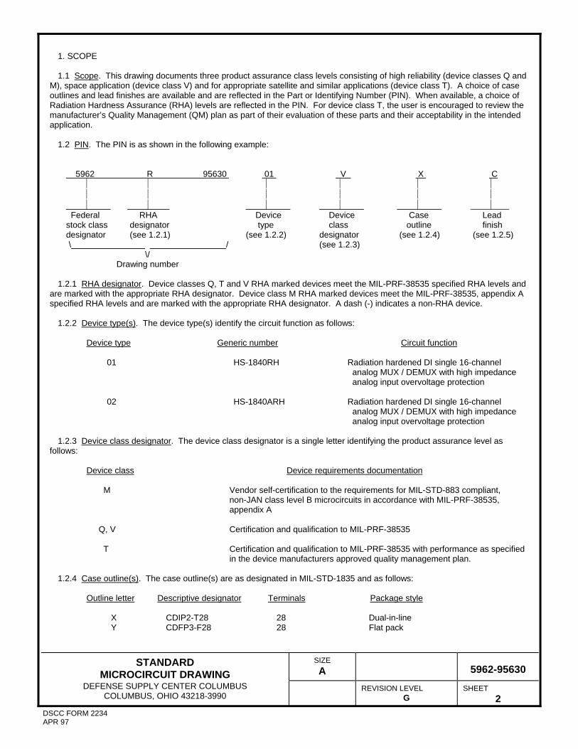
1. SCOPE 1.1 Scope. This drawing documents three product assurance class levels consisting of high reliability (device classes Q and M), space application (device class V) and for appropriate satellite and similar applications (device class T). A choice of case outlines and lead finishes are available and are reflected in the Part or Identifying Number (PIN). When available, a choice of Radiation Hardness Assurance (RHA) levels are reflected in the PIN. For device class T, the user is encouraged to review the manufacturer’s Quality Management (QM) plan as part of their evaluation of these parts and their acceptability in the intended application. 1.2 PIN. The PIN is as shown in the following example:
5962 R 95630 01 V X C
Federal RHA Device Device Case Lead stock class designator type class outline finish designator (see 1.2.1) (see 1.2.2) designator (see 1.2.4) (see 1.2.5)
\ / (see 1.2.3) \/ Drawing number 1.2.1 RHA designator. Device classes Q, T and V RHA marked devices meet the MIL-PRF-38535 specified RHA levels and are marked with the appropriate RHA designator. Device class M RHA marked devices meet the MIL-PRF-38535, appendix A specified RHA levels and are marked with the appropriate RHA designator. A dash (-) indicates a non-RHA device. 1.2.2 Device type(s). The device type(s) identify the circuit function as follows:
Device type Generic number Circuit function
01 HS-1840RH Radiation hardened DI single 16-channel analog MUX / DEMUX with high impedance analog input overvoltage protection
02 HS-1840ARH Radiation hardened DI single 16-channel analog MUX / DEMUX with high impedance analog input overvoltage protection
1.2.3 Device class designator. The device class designator is a single letter identifying the product assurance level as follows:
Device class Device requirements documentation
M Vendor self-certification to the requirements for MIL-STD-883 compliant, non-JAN class level B microcircuits in accordance with MIL-PRF-38535, appendix A
Q, V Certification and qualification to MIL-PRF-38535
T Certification and qualification to MIL-PRF-38535 with performance as specified in the device manufacturers approved quality management plan. 1.2.4 Case outline(s). The case outline(s) are as designated in MIL-STD-1835 and as follows:
Outline letter Descriptive designator Terminals Package style
X CDIP2-T28 28 Dual-in-line Y CDFP3-F28 28 Flat pack

STANDARD MICROCIRCUIT DRAWING
SIZE A
5962-95630
DEFENSE SUPPLY CENTER COLUMBUS COLUMBUS, OHIO 43218-3990
REVISION LEVEL G
SHEET 3
DSCC FORM 2234 APR 97
1.2.5 Lead finish. The lead finish is as specified in MIL-PRF-38535 for device classes Q, T and V or MIL-PRF-38535, appendix A for device class M. 1.3 Absolute maximum ratings. 1/
Supply voltage between V+ and V- : Device type 01 ........................................................................... +40 V Device type 02 ........................................................................... +33 V Supply voltage between V+ and GND : Device type 01 ........................................................................... +20 V Device type 02 ........................................................................... +16.5 V Supply voltage between V- and GND : Device type 01 ........................................................................... -20 V Device type 02 ........................................................................... -16.5 V VREF to GND : Device type 01 ........................................................................... +20 V Device type 02 ........................................................................... +16.5 V Digital input overvoltage range ...................................................... ((GND) - 4 V) ≤ VA ≤ ((VREF) + 4 V) Analog input overvoltage range (power on/off): Device type 01 ........................................................................... -25 V ≤ VS ≤ +25 V Device type 02 ........................................................................... -35 V ≤ VS ≤ +35 V Storage temperature range ............................................................ -65°C to +150°C Maximum package power dissipation (PD): 2/ Case X ..................................................................................... 1600 mW Case Y ..................................................................................... 1400 mW Lead temperature (soldering, 10 seconds) .................................... +275°C Thermal resistance, junction-to-case (θJC) .................................... See MIL-STD-1835 Thermal resistance, junction-to-ambient (θJA): Case X ..................................................................................... 83.1°C/W Case Y ..................................................................................... 49.1°C/W
1.4 Recommended operating conditions.
Positive supply voltage (V+) ........................................................... +15 V Negative supply voltage (V-)........................................................... -15 V VREF .............................................................................................. 5 V dc VAH ................................................................................................ 4.0 V dc VAL ................................................................................................ 0.8 V dc VEN ................................................................................................ 0.8 V dc Ambient operating temperature range (TA) ................................... -55°C to +125°C
____ 1/ Stresses above the absolute maximum rating may cause permanent damage to the device. Extended operation at the maximum levels may degrade performance and affect reliability. 2/ The derating factor for case X shall be 20.4 mW/°C, above TA = +95°C, and for case Y shall be 18.5 mW/°C above TA = +95°C.

STANDARD MICROCIRCUIT DRAWING
SIZE A
5962-95630
DEFENSE SUPPLY CENTER COLUMBUS COLUMBUS, OHIO 43218-3990
REVISION LEVEL G
SHEET 4
DSCC FORM 2234 APR 97
1.5 Radiation features.
SEP effective let no upsets: Device type 01 ............................................................................ 110 MeV/cm2/mg Device type 02 ............................................................................ 120 MeV/cm2/mg Maximum total dose available: (dose rate = 50 – 300 rad(Si)/s)
Device classes M, Q, and V: Device type 01 .......................................................................... 200 Krads (Si) Device type 02 .......................................................................... 300 Krads (Si)
Device class T: Device type 02 .......................................................................... 100 Krads (Si)
Dose rate upset: Device type 01 ............................................................................ >1 x 10⁸ rad(Si)/s Device type 02 ............................................................................ Not tested Latch up ......................................................................................... None 3/
2. APPLICABLE DOCUMENTS 2.1 Government specification, standards, and handbooks. The following specification, standards, and handbooks form a part of this drawing to the extent specified herein. Unless otherwise specified, the issues of these documents are those cited in the solicitation or contract. DEPARTMENT OF DEFENSE SPECIFICATION MIL-PRF-38535 - Integrated Circuits, Manufacturing, General Specification for. DEPARTMENT OF DEFENSE STANDARDS MIL-STD-883 - Test Method Standard Microcircuits. MIL-STD-1835 - Interface Standard Electronic Component Case Outlines. DEPARTMENT OF DEFENSE HANDBOOKS MIL-HDBK-103 - List of Standard Microcircuit Drawings. MIL-HDBK-780 - Standard Microcircuit Drawings.
(Copies of these documents are available online at http://assist.daps.dla.mil/quicksearch/ or http://assist.daps.dla.mil or from the Standardization Document Order Desk, 700 Robbins Avenue, Building 4D, Philadelphia, PA 19111-5094.) 2.2 Order of precedence. In the event of a conflict between the text of this drawing and the references cited herein, the text of this drawing takes precedence. Nothing in this document, however, supersedes applicable laws and regulations unless a specific exemption has been obtained. _____ 3/ Guaranteed by process design, but not tested, unless specified in table I herein.
rbenson
Highlight
rbenson
Highlight
rbenson
Highlight
rbenson
Highlight
rbenson
Highlight

STANDARD MICROCIRCUIT DRAWING
SIZE A
5962-95630
DEFENSE SUPPLY CENTER COLUMBUS COLUMBUS, OHIO 43218-3990
REVISION LEVEL G
SHEET 5
DSCC FORM 2234 APR 97
3. REQUIREMENTS 3.1 Item requirements. The individual item requirements for device classes Q, T and V shall be in accordance with MIL-PRF-38535 and as specified herein or as modified in the device manufacturer's Quality Management (QM) plan. The modification in the QM plan shall not affect the form, fit, or function as described herein. The individual item requirements for device class M shall be in accordance with MIL-PRF-38535, appendix A for non-JAN class level devices and as specified herein. 3.1.1 Microcircuit die. For the requirements for microcircuit die, see appendix A to this document. 3.2 Design, construction, and physical dimensions. The design, construction, and physical dimensions shall be as specified in MIL-PRF-38535 and herein for device classes Q, T and V or MIL-PRF-38535, appendix A and herein for device class M. 3.2.1 Case outlines. The case outlines shall be in accordance with 1.2.4 herein. 3.2.2 Terminal connections. The terminal connections shall be as specified on figure 1. 3.2.3 Truth table. The truth table shall be as specified on figure 2. 3.2.4 Logic diagrams. The logic diagrams shall be as specified on figure 3. 3.2.5 Radiation exposure circuit. The radiation exposure circuit shall be as specified on figure 4. 3.3 Electrical performance characteristics and postirradiation parameter limits. Unless otherwise specified herein, the electrical performance characteristics and postirradiation parameter limits are as specified in table I and shall apply over the full ambient operating temperature range. 3.4 Electrical test requirements. The electrical test requirements shall be the subgroups specified in table IIA. The electrical tests for each subgroup are defined in table I. 3.5 Marking. The part shall be marked with the PIN listed in 1.2 herein. In addition, the manufacturer's PIN may also be marked. For packages where marking of the entire SMD PIN number is not feasible due to space limitations, the manufacturer has the option of not marking the "5962-" on the device. For RHA product using this option, the RHA designator shall still be marked. Marking for device classes Q, T and V shall be in accordance with MIL-PRF-38535. Marking for device class M shall be in accordance with MIL-PRF-38535, appendix A. 3.5.1 Certification/compliance mark. The certification mark for device classes Q, T and V shall be a "QML" or "Q" as required in MIL-PRF-38535. The compliance mark for device class M shall be a "C" as required in MIL-PRF-38535, appendix A. 3.6 Certificate of compliance. For device classes Q, T and V, a certificate of compliance shall be required from a QML-38535 listed manufacturer in order to supply to the requirements of this drawing (see 6.6.1 herein). For device class M, a certificate of compliance shall be required from a manufacturer in order to be listed as an approved source of supply in MIL-HDBK-103 (see 6.6.2 herein). The certificate of compliance submitted to DSCC-VA prior to listing as an approved source of supply for this drawing shall affirm that the manufacturer's product meets, for device classes Q, T and V, the requirements of MIL-PRF-38535 and herein or for device class M, the requirements of MIL-PRF-38535, appendix A and herein. 3.7 Certificate of conformance. A certificate of conformance as required for device classes Q, T and V in MIL-PRF-38535 or for device class M in MIL-PRF-38535, appendix A shall be provided with each lot of microcircuits delivered to this drawing. 3.8 Notification of change for device class M. For device class M, notification to DSCC-VA of change of product (see 6.2 herein) involving devices acquired to this drawing is required for any change that affects this drawing. 3.9 Verification and review for device class M. For device class M, DSCC, DSCC's agent, and the acquiring activity retain the option to review the manufacturer's facility and applicable required documentation. Offshore documentation shall be made available onshore at the option of the reviewer. 3.10 Microcircuit group assignment for device class M. Device class M devices covered by this drawing shall be in microcircuit group number 82 (see MIL-PRF-38535, appendix A).

STANDARD MICROCIRCUIT DRAWING
SIZE A
5962-95630
DEFENSE SUPPLY CENTER COLUMBUS COLUMBUS, OHIO 43218-3990
REVISION LEVEL G
SHEET 6
DSCC FORM 2234 APR 97
TABLE I. Electrical performance characteristics.
Test Symbol
Conditions 1/
-55°C ≤ TA ≤ +125°C unless otherwise specified
Group A
subgroups
Device
type
Limits
Unit
Min
Max
Input leakage current, 2/ address or enable pins
IAH
Measure inputs sequentially, ground all used pins.
1,2,3
01,02
-1.0
1.0
µA
M, D, P, L, R, F
1 3/
-1.0
1.0
IAL
1,2,3
-1.0
1.0
µA
M, D, P, L, R, F
1 3/
-1.0
1.0
Leakage current into the source terminal of an off switch
IS(OFF)
VS = -10 V, all unused inputs and output equal +10 V, see figure 5
1
01,02
-10
+10
nA
2,3
-100
+100
M, D, P, L, R, F 4/
1 3/
-100
+100
VS = +10 V, all unused inputs and output equal -10 V, see figure 5
1
-10
+10
nA
2,3
-100
+100
M, D, P, L, R, F 4/
1 3/
-100
+100
Leakage current into the source terminal of an off switch with power off
IS(OFF) power off
VS = +25 V, VA = 0 V, VEN = 0 V, V- = 0 V, V+ = 0 V, VREF = 0 V, all unused inputs tied to GND, see figure 5
1
01,02
-50
+50
nA
2,3
-100
+100
M, D, P, L, R, F
1 3/
-100
+100
Leakage current into the source terminal of an off switch with overvoltage applied
IS(OFF) over- voltage
VD = 0 V, all unused inputs tied to GND, see figure 5
1,2,3
01,02
-1
+1
µA
5/
M, D, P, L, R, F 4/
1 3/
-1.5
+1.5
VD = 0 V, all unused inputs tied to GND, see figure 5
1,2,3
-1
+1
µA
6/
M, D, P, L, R, F 4/
1 3/
-1.5
+1.5
See footnotes at end table.

STANDARD MICROCIRCUIT DRAWING
SIZE A
5962-95630
DEFENSE SUPPLY CENTER COLUMBUS COLUMBUS, OHIO 43218-3990
REVISION LEVEL G
SHEET 7
DSCC FORM 2234 APR 97
TABLE I. Electrical performance characteristics - Continued.
Test Symbol
Conditions 1/
-55°C ≤ TA ≤ +125°C unless otherwise specified
Group A
subgroups
Device
type
Limits
Unit
Min
Max
Leakage current into the drain terminal of an off switch with overvoltage applied
ID(OFF) over- voltage
VD = 0 V, all unused inputs tied to GND, see figure 5
1,2,3
01,02
-1
+1
µA
5/
M, D, P, L, R, F 4/
1 3/
-1
+1
VD = 0 V, all unused inputs tied to GND, see figure 5
1,2,3
-1
+1
µA
6/
M, D, P, L, R, F 4/
1 3/
-1
+1
Leakage current into the drain terminal of an off switch
ID(OFF)
VD = -10 V, all unused inputs = +10 V, see figure 5
1
01,02
-10
+10
nA
2,3
-100
+100
M, D, P, L, R, F 4/
1 3/
-100
+100
Leakage current into the drain terminal of an off switch
ID(OFF)
VD = +10 V, all unused inputs = -10 V, see figure 5
1
01,02
-10
+10
nA
2,3
-100
+100
M, D, P, L, R, F 4/
1 3/
-100
+100
Leakage current from an on driver into the switch (drain and source)
ID(ON)
VS = +10 V, VD = +10 V, VEN = 0.8 V, all unused input = -10 V, see figure 5
1
01,02
-10
+10
nA
2,3
-100
+100
M, D, P, L, R, F 7/
1 3/
-100
+100
VS = -10 V, VD = -10 V, VEN = 0.8 V, all unused input = +10 V, see figure 5
1
-10
+10
nA
2,3
-100
+100
M, D, P, L, R, F 7/
1 3/
-100
+100

STANDARD MICROCIRCUIT DRAWING
SIZE A
5962-95630
DEFENSE SUPPLY CENTER COLUMBUS COLUMBUS, OHIO 43218-3990
REVISION LEVEL G
SHEET 8
DSCC FORM 2234 APR 97
TABLE I. Electrical performance characteristics - Continued.
Test Symbol
Conditions 1/
-55°C ≤ TA ≤ +125°C unless otherwise specified
Group A
subgroups
Device
type
Limits
Unit
Min
Max
Positive supply current
I+
VA = 0 V, VEN = 0.8 V
1,2,3
01,02
0.05
0.5
mA
M, D, P, L, R, F 7/
1 3/
0.05
0.5
Negative power supply
I-
VA = 0 V, VEN = 0.8 V
1,2,3
0.05
0.5
mA
M, D, P, L, R, F 7/
1 3/
0.05
0.5
Positive standby supply current
+ISBY
VA = 0 V, VEN = 4.0 V
1,2,3
01,02
0.05
0.5
mA
M, D, P, L, R, F 4/
1 3/
0.05
0.5
Negative standby power supply
-ISBY
VA = 0 V, VEN = 4.0 V
1,2,3
0.05
0.5
mA
M, D, P, L, R, F 4/
1 3/
0.05
0.5
Switch on resistance
RDS(ON)
VS = +15 V, ID = -1 mA, VEN = 0.8 V, see figure 5
1,2,3
01
---
1.0
kΩ
02
0.5
3.0
M, D, P, L, R, F 7/
1 3/
01
---
1.0
02
0.5
3.0
VS = -5 V, ID = +1 mA, VEN = 0.8 V, see figure 5
1,2,3
01
---
4.0
02
0.5
3.0
M, D, P, L, R, F 7/
1 3/
01
---
4.0
02
0.5
3.0
VS = +5 V, ID = -1 mA, VEN = 0.8 V, see figure 5
1,2,3
01
---
2.5
02
0.5
3.0
M, D, P, L, R, F 7/
1 3/
01
---
2.5
02
0.5
3.0
See footnotes at end of table.

STANDARD MICROCIRCUIT DRAWING
SIZE A
5962-95630
DEFENSE SUPPLY CENTER COLUMBUS COLUMBUS, OHIO 43218-3990
REVISION LEVEL G
SHEET 9
DSCC FORM 2234 APR 97
TABLE I. Electrical performance characteristics - Continued.
Test
Symbol
Conditions 1/ -55°C ≤ TA ≤ +125°C
unless otherwise specified
Group A
subgroups
Device
type
Limits
Unit
Min
Max
Capacitance: digital input
CA
V+ = V- = 0 V, f = 1 MHz, TA = +25°C, see 4.4.1c
4
01,02
7
pF
Capacitance: channel input
CS(OFF)
V+ = V- = 0 V, f = 1 MHz, TA = +25°C, see 4.4.1c
4
01,02
5
pF
Capacitance: channel output
CD(OFF)
V+ = V- = 0 V, f = 1 MHz, TA = +25°C, see 4.4.1c
4
01,02
50
pF
Off isolation input or output
VISO
VEN = 4.0 V, f = 200 kHz, CL = 7 pF, RL = 1 kΩ, VS = 3 VRMS, TA = +25°C, see 4.4.1c
4
01,02
-45
dB
Functional test
See 4.4.1d
7,8A,8B
01,02
Break-before-make time delay
tD
CL = 50 pF, RL = 1 kΩ, see figure 6
9
01,02
25
ns
10,11
5
M, D, P, L, R, F 4/ 7/ 8/
9 3/
5
Propagation delay time address inputs to I/O channels
tON(A), tOFF(A)
CL = 50 pF, RL = 10 kΩ, see figure 6
9
01
0.6
µs
02
1.25
10,11
01
1.0
02
1.5
M, D, P, L, R, F 4/ 7/ 8/
9 3/
01
3.0
02
1.5
See footnotes at end of table.

STANDARD MICROCIRCUIT DRAWING
SIZE A
5962-95630
DEFENSE SUPPLY CENTER COLUMBUS COLUMBUS, OHIO 43218-3990
REVISION LEVEL G
SHEET 10
DSCC FORM 2234 APR 97
TABLE I. Electrical performance characteristics - Continued.
Test
Symbol
Conditions 1/ -55°C ≤ TA ≤ +125°C
unless otherwise specified
Group A
subgroups
Device
type
Limits
Unit
Min
Max
Propagation delay time enable to I/O channels
tON(EN), tOFF(EN)
CL = 50 pF, RL = 1 kΩ, see figure 6
9
01
0.6
µs
02
1.25
10,11
01
1.0
02
1.5
M, D, P, L, R, F 4/ 7/ 8/
9 3/
01
3.0
02
1.5
1/ VAH (logic level high) = 4.0 V dc, VAL (logic level low) = 0.8 V dc, V+ = +15 V dc, V- = -15 V dc, VEN = 4.0 V unless
otherwise specified, and VREF = 5.0 V dc. 2/ Input current of one node. 3/ Devices supplied to this drawing will meet all levels M, D, P, L, R, for device type 01 (device classes M, Q, and V) and levels M, D, P, L, R, F for device type 02 (device classes M, Q, or V) and levels M, D, P, L, R, for device type 02 (device class T). However, device type 01(device classes M, Q, and V) is only tested at the "R" level and device type 02 (device classes M, Q, and V) is only tested at the "F" level, and device type 02 (class T) is only tested at the “R” level. (see paragraph 1.5 herein). Pre and Post irradiation values are identical unless otherwise specified in Table I.
When performing post irradiation electrical measurements for any RHA level, TA = +25°C.
4/ VEN = 4.5 V
5/ For device type 01, VS = +25 V. For device type 02, VS = +35 V.
6/ For device type 01, VS = -25 V. For device type 02, VS = -35 V.
7/ VEN = 0.5 V
8/ VAH = 4.5 V and VAL = 0.5 V

STANDARD MICROCIRCUIT DRAWING
SIZE A
5962-95630
DEFENSE SUPPLY CENTER COLUMBUS COLUMBUS, OHIO 43218-3990
REVISION LEVEL G
SHEET 11
DSCC FORM 2234 APR 97
Device types 01 and 02
Case outlines X and Y Terminal number Terminal symbol
1 V+
2 NC
3 NC
4 IN 16
5 IN 15
6 IN 14
7 IN 13
8 IN 12
9 IN 11
10 IN 10
11 IN 9
12 GND
13 VREF
14 A3
15 A2
16 A1
17 A0
18 EN
19 IN 1
20 IN 2
21 IN 3
22 IN 4
23 IN 5
24 IN 6
25 IN 7
26 IN 8
27 V-
28 OUT NC = No connection
FIGURE 1. Terminal connections.

STANDARD MICROCIRCUIT DRAWING
SIZE A
5962-95630
DEFENSE SUPPLY CENTER COLUMBUS COLUMBUS, OHIO 43218-3990
REVISION LEVEL G
SHEET 12
DSCC FORM 2234 APR 97
Truth table
A3 A2 A1 A0 EN On channel
X X X X H None
L L L L L 1
L L L H L 2
L L H L L 3
L L H H L 4
L H L L L 5
L H L H L 6
L H H L L 7
L H H H L 8
H L L L L 9
H L L H L 10
H L H L L 11
H L H H L 12
H H L L L 13
H H L H L 14
H H H L L 15
H H H H L 16
FIGURE 2. Truth table.

STANDARD MICROCIRCUIT DRAWING
SIZE A
5962-95630
DEFENSE SUPPLY CENTER COLUMBUS COLUMBUS, OHIO 43218-3990
REVISION LEVEL G
SHEET 13
DSCC FORM 2234 APR 97
FIGURE 3. Logic diagram.

STANDARD MICROCIRCUIT DRAWING
SIZE A
5962-95630
DEFENSE SUPPLY CENTER COLUMBUS COLUMBUS, OHIO 43218-3990
REVISION LEVEL G
SHEET 14
DSCC FORM 2234 APR 97
FIGURE 4. Radiation exposure circuit.

STANDARD MICROCIRCUIT DRAWING
SIZE A
5962-95630
DEFENSE SUPPLY CENTER COLUMBUS COLUMBUS, OHIO 43218-3990
REVISION LEVEL G
SHEET 15
DSCC FORM 2234 APR 97
FIGURE 5. Test circuits for dc levels.

STANDARD MICROCIRCUIT DRAWING
SIZE A
5962-95630
DEFENSE SUPPLY CENTER COLUMBUS COLUMBUS, OHIO 43218-3990
REVISION LEVEL G
SHEET 16
DSCC FORM 2234 APR 97
FIGURE 6. Test circuits and waveforms for ac levels.

STANDARD MICROCIRCUIT DRAWING
SIZE A
5962-95630
DEFENSE SUPPLY CENTER COLUMBUS COLUMBUS, OHIO 43218-3990
REVISION LEVEL G
SHEET 17
DSCC FORM 2234 APR 97
4. VERIFICATION
4.1 Sampling and inspection. For device classes Q and V, sampling and inspection procedures shall be in accordance with MIL-PRF-38535 or as modified in the device manufacturer's (QM) plan, including screening (4.2), qualification (4.3), and conformance inspection (4.4). The modification in the QM plan shall not affect the form, fit, or function as described herein.
For device class T, sampling and inspection procedures shall be in accordance with MIL-PRF-38535 or as modified in the device manufacturer's (QM) plan, including screening, qualification, and conformance inspection. The performance envelope and reliability information shall be as specified in the manufacturer’s QM plan. For device class M, sampling and inspection procedures shall be in accordance with MIL-PRF-38535, appendix A. 4.2 Screening. For device classes Q and V, screening shall be in accordance with MIL-PRF-38535, and shall be conducted on all devices prior to qualification and technology conformance inspection. For device class M, screening shall be in accordance with method 5004 of MIL-STD-883, and shall be conducted on all devices prior to quality conformance inspection. For device class T, screening shall be in accordance with the device manufacturer’s Quality Management (QM) plan, and shall be conducted on all devices prior to qualification and technology conformance inspection. 4.2.1 Additional criteria for device class M.
a. Burn-in test, method 1015 of MIL-STD-883.
(1) Test condition A, B, C, or D. The test circuit shall be maintained by the manufacturer under document revision level control and shall be made available to the preparing or acquiring activity upon request. The test circuit shall specify the inputs, outputs, biases, and power dissipation, as applicable, in accordance with the intent specified in method 1015.
(2) TA = +125°C, minimum.
b. Interim and final electrical test parameters shall be as specified in table IIA herein.
4.2.2 Additional criteria for device classes Q, T and V.
a. The burn-in test duration, test condition and test temperature, or approved alternatives shall be as specified in the device manufacturer's QM plan in accordance with MIL-PRF-38535. The burn-in test circuit shall be maintained under document revision level control of the device manufacturer's Technology Review Board (TRB) in accordance with
MIL-PRF-38535 and shall be made available to the acquiring or preparing activity upon request. The test circuit shall specify the inputs, outputs, biases, and power dissipation, as applicable, in accordance with the intent specified in method 1015 of MIL-STD-883.
b. For devices classes Q, T, and V interim and final electrical test parameters shall be as specified in table IIA herein.
c. Additional screening for device class V beyond the requirements of device class Q shall be as specified in MIL-PRF-38535, appendix B or as modified in the device manufacturer’s Quality Management (QM) plan.
4.3 Qualification inspection for device classes Q, T and V. Qualification inspection for device classes Q and V shall be in accordance with MIL-PRF-38535. Qualification inspection for device class T shall be in accordance with the device manufacturer’s Quality Management (QM) plan. Inspections to be performed shall be those specified in MIL-PRF-38535 and herein for groups A, B, C, D, and E inspections (see 4.4.1 through 4.4.4). 4.4 Conformance inspection. Technology conformance inspection for classes Q and V shall be in accordance with MIL-PRF-38535 as specified in the QM plan including groups A, B, C, D, and E inspections and as specified herein. Quality conformance inspection for device class M shall be in accordance with MIL-PRF-38535, appendix A and as specified herein. Inspections to be performed for device class M shall be those specified in method 5005 of MIL-STD-883 and herein for groups A, B, C, D, and E inspections (see 4.4.1 through 4.4.4). Technology conformance inspection for class T shall be in accordance with the device manufacturer’s Quality Management (QM) plan.
STANDARD MICROCIRCUIT DRAWING
SIZE A
5962-95630
DEFENSE SUPPLY CENTER COLUMBUS COLUMBUS, OHIO 43218-3990
REVISION LEVEL G
SHEET 18
DSCC FORM 2234 APR 97
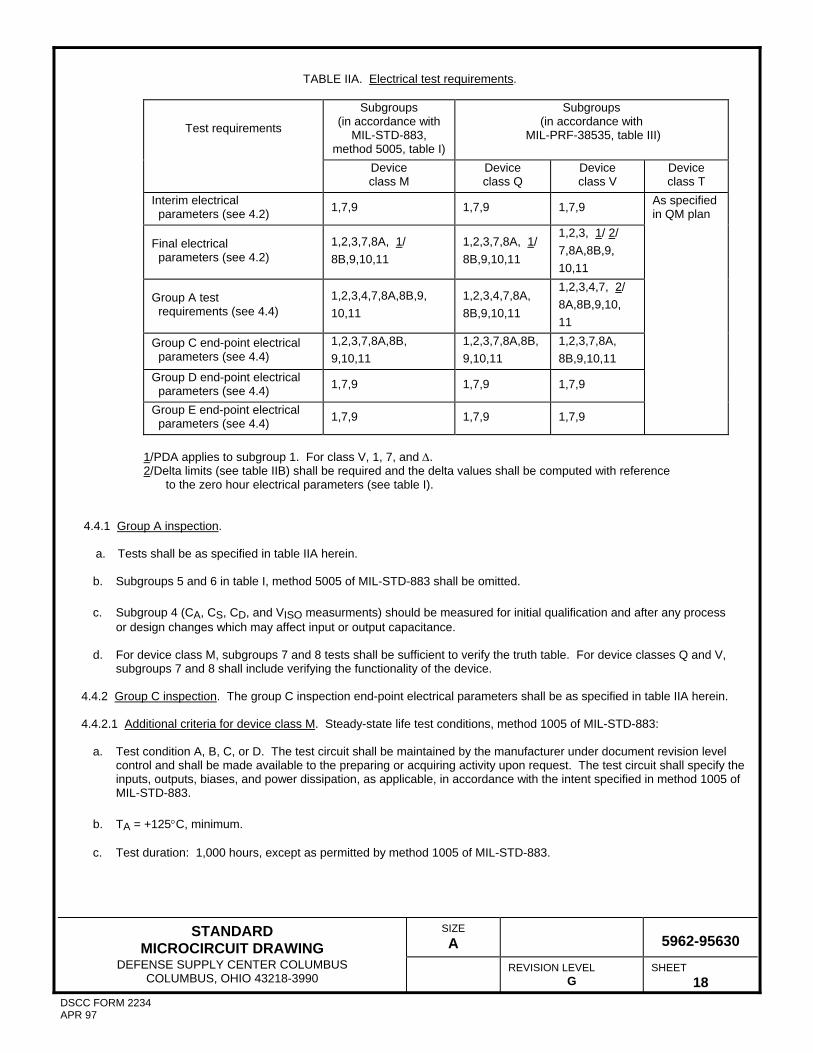
TABLE IIA. Electrical test requirements.
Test requirements
Subgroups (in accordance with
MIL-STD-883, method 5005, table I)
Subgroups (in accordance with
MIL-PRF-38535, table III)
Device class M
Device class Q
Device class V
Device class T
Interim electrical parameters (see 4.2) 1,7,9 1,7,9 1,7,9 As specified
in QM plan
Final electrical parameters (see 4.2)
1,2,3,7,8A, 1/ 8B,9,10,11
1,2,3,7,8A, 1/ 8B,9,10,11
1,2,3, 1/ 2/ 7,8A,8B,9, 10,11
Group A test requirements (see 4.4)
1,2,3,4,7,8A,8B,9, 10,11
1,2,3,4,7,8A, 8B,9,10,11
1,2,3,4,7, 2/ 8A,8B,9,10, 11
Group C end-point electrical parameters (see 4.4)
1,2,3,7,8A,8B, 9,10,11
1,2,3,7,8A,8B, 9,10,11
1,2,3,7,8A, 8B,9,10,11
Group D end-point electrical parameters (see 4.4) 1,7,9 1,7,9 1,7,9
Group E end-point electrical parameters (see 4.4) 1,7,9 1,7,9 1,7,9
1/ PDA applies to subgroup 1. For class V, 1, 7, and ∆. 2/ Delta limits (see table IIB) shall be required and the delta values shall be computed with reference to the zero hour electrical parameters (see table I).
4.4.1 Group A inspection.
a. Tests shall be as specified in table IIA herein. b. Subgroups 5 and 6 in table I, method 5005 of MIL-STD-883 shall be omitted. c. Subgroup 4 (CA, CS, CD, and VISO measurments) should be measured for initial qualification and after any process or design changes which may affect input or output capacitance. d. For device class M, subgroups 7 and 8 tests shall be sufficient to verify the truth table. For device classes Q and V, subgroups 7 and 8 shall include verifying the functionality of the device. 4.4.2 Group C inspection. The group C inspection end-point electrical parameters shall be as specified in table IIA herein. 4.4.2.1 Additional criteria for device class M. Steady-state life test conditions, method 1005 of MIL-STD-883:
a. Test condition A, B, C, or D. The test circuit shall be maintained by the manufacturer under document revision level control and shall be made available to the preparing or acquiring activity upon request. The test circuit shall specify the inputs, outputs, biases, and power dissipation, as applicable, in accordance with the intent specified in method 1005 of MIL-STD-883.
b. TA = +125°C, minimum.
c. Test duration: 1,000 hours, except as permitted by method 1005 of MIL-STD-883.

STANDARD MICROCIRCUIT DRAWING
SIZE A
5962-95630
DEFENSE SUPPLY CENTER COLUMBUS COLUMBUS, OHIO 43218-3990
REVISION LEVEL G
SHEET 19
DSCC FORM 2234 APR 97
TABLE IIB. Burn-in delta parameters (+25°C) and group C delta parameters.
Parameters
Symbol
Conditions
Delta limits Input leakage current, address, or enable pins
IAH
Measure inputs sequentially, ground all unbiased pins
±100 nA
Leakage current into the source terminal of an "Off" switch
+IS(OFF)
VS = +10 V, all unused and output = -10 V, VEN = 4.0 V
±20 nA
-IS(OFF)
VS = -10 V, all unused inputs and outputs = +10 V, VEN = 4.0 V
±20 nA
Leakage current into the drain terminal of an "Off" switch
+ID(OFF)
VD = +10 V, all unused inputs = -10 V, VEN = 4.0 V
±20 nA
-ID(OFF)
VD = -10 V, all unused inputs = +10 V, VEN = 4.0 V
±20 nA
Leakage current from an "On" driver into the switch (drain and source)
+ID(ON)
VS = +10 V, all unused inputs = -10 V, VEN = 0.8 V, VD = +10 V
±20 nA
-ID(ON)
VS = -10 V, all unused inputs = +10 V, VD = -10 V, VEN = 0.8 V
±20 nA
Switch on resistance
R(ON)
VS = +15 V, ID = -1 mA, VEN = 0.8 V
±150 Ω
VS = -5 V, ID = +1 mA, VEN = 0.8 V
±250 Ω
Positive supply current
I+
VEN = 0.8 V
±50 µA
Negative supply current
I-
VEN = 0.8 V
±50 µA
Positive standby supply current
+ISBY
VEN = 4.0 V
±50 µA
Negative standby supply current
-ISBY
VEN = 4.0 V
±50 µA

STANDARD MICROCIRCUIT DRAWING
SIZE A
5962-95630
DEFENSE SUPPLY CENTER COLUMBUS COLUMBUS, OHIO 43218-3990
REVISION LEVEL G
SHEET 20
DSCC FORM 2234 APR 97
4.4.2.2 Additional criteria for device classes Q, T and V. The steady-state life test duration, test condition and test temperature, or approved alternatives shall be as specified in the device manufacturer's QM plan in accordance with MIL-PRF-38535. The test circuit shall be maintained under document revision level control by the device manufacturer's TRB in accordance with MIL-PRF-38535 and shall be made available to the acquiring or preparing activity upon request. The test circuit shall specify the inputs, outputs, biases, and power dissipation, as applicable, in accordance with the intent specified in method 1005 of MIL-STD-883. 4.4.3 Group D inspection. The group D inspection end-point electrical parameters shall be as specified in table IIA herein. 4.4.4 Group E inspection. Group E inspection is required only for parts intended to be marked as radiation hardness assured (see 3.5 herein). RHA levels for device classes M, Q and V shall be as specified in MIL-PRF-38535. End-point electrical parameters shall be as specified in table IIA herein. For device class T, the RHA requirements shall be in accordance with the Class T radiation requirements of MIL-PRF-38535. The end-point electrical parameters for class T devices shall be as specified in Table I, Group A subgroups, or as modified in the QM plan. 4.4.4.1 Total dose irradiation testing. Total dose irradiation testing shall be performed in accordance with MIL-STD-883 method 1019 condition A and as specified herein. For device class T, the total dose requirements shall be in accordance with the class T radiation requirements of MIL-PRF-38535 ( see 1.5 herein ).
4.4.4.1.1 Accelerated aging test. Accelerated aging tests shall be performed on all devices requiring a RHA level greater than 5k rads(Si). The post-anneal end-point electrical parameter limits shall be as specified in table I herein and shall be the pre-irradiation end-point electrical parameter limit at 25°C ±5°C. Testing shall be performed at initial qualification and after any design or process changes which may affect the RHA response of the device.
4.4.4.2 Dose rate induced latchup testing. When specified in the purchase order or contract, dose rate induced latchup testing shall be performed in accordance with test method 1020 of MIL-STD-883 and as specified herein (see 1.5 herein). Tests shall be performed on devices, SEC, or approved test structures at technology qualification and after any design or process changes which may effect the RHA capability of the process.
4.4.4.3 Dose rate upset testing. When specified in the purchase order or contract, dose rate upset testing shall be performed in accordance with test method 1021 of MIL-STD-883 and herein (see 1.5 herein).
a. Transient dose rate upset testing shall be performed at initial qualification and after any design or process changes which may affect the RHA performance of the devices. Test 10 devices with 0 defects unless otherwise specified.
b. Transient dose rate upset testing for class Q, T, and V devices shall be performed as specified by a TRB approved
radiation hardness assurance plan and MIL-PRF-38535.
4.4.4.4 Single event phenomena (SEP). When specified in the purchase order or contract, SEP testing shall be required on class T and V devices (see 1.5 herein). SEP testing shall be performed on a technology process on the Standard Evaluation Circuit (SEC) or alternate SEP test vehicle as approved by the qualifying activity at initial qualification and after any design or process changes which may affect the upset or latchup characteristics. The recommended test conditions for SEP are as follows:
a. The ion beam angle of incidence shall be between normal to the die surface and 60° to the normal, inclusive (i.e. 0° ≤ angle ≤ 60°). No shadowing of the ion beam due to fixturing or package related effects is allowed.
b. The fluence shall be ≥ 100 errors or ≥ 106 ions/cm2.
c. The flux shall be between 102 and 105 ions/cm2/s. The cross-section shall be verified to be flux independent by measuring the cross-section at two flux rates which differ by at least an order of magnitude.
d. The particle range shall be ≥ 20 micron in silicon.
e. The test temperature shall be +25°C and the maximum rated operating temperature ±10°C.
f. Bias conditions shall be defined by the manufacturer for the latchup measurements.
g. Test four devices with zero failures.
STANDARD MICROCIRCUIT DRAWING
SIZE A
5962-95630
DEFENSE SUPPLY CENTER COLUMBUS COLUMBUS, OHIO 43218-3990
REVISION LEVEL G
SHEET 21
DSCC FORM 2234 APR 97
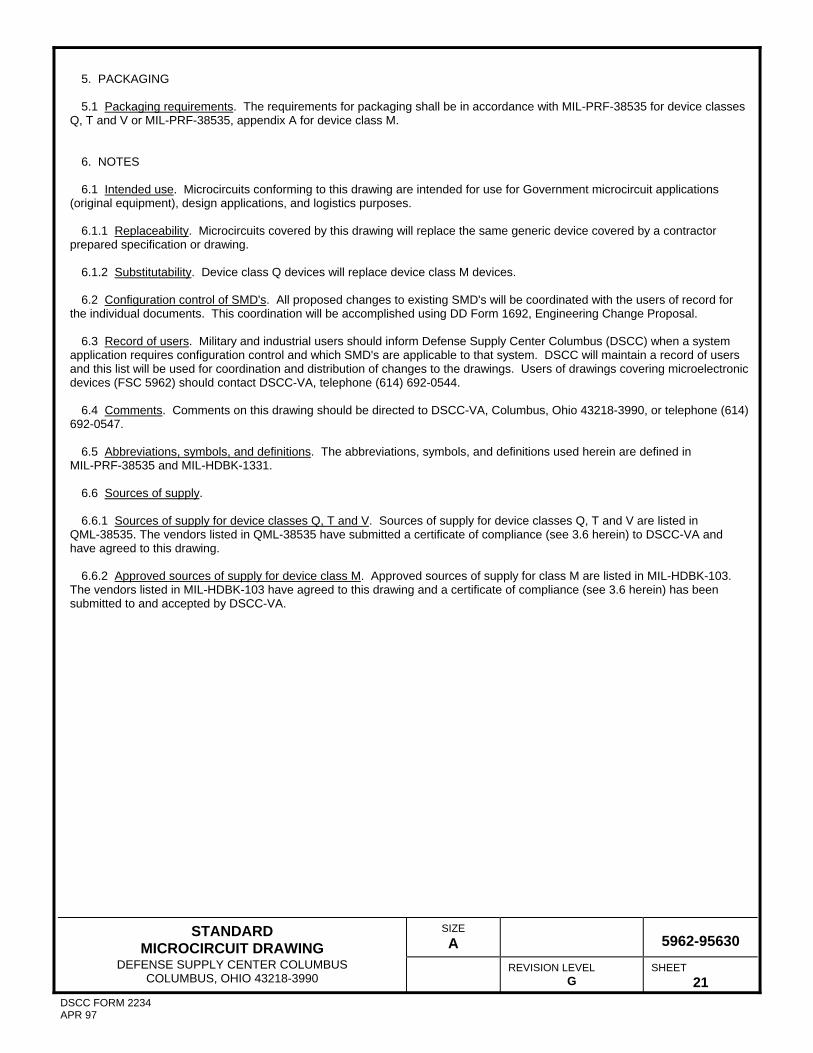
5. PACKAGING 5.1 Packaging requirements. The requirements for packaging shall be in accordance with MIL-PRF-38535 for device classes Q, T and V or MIL-PRF-38535, appendix A for device class M. 6. NOTES 6.1 Intended use. Microcircuits conforming to this drawing are intended for use for Government microcircuit applications (original equipment), design applications, and logistics purposes. 6.1.1 Replaceability. Microcircuits covered by this drawing will replace the same generic device covered by a contractor prepared specification or drawing. 6.1.2 Substitutability. Device class Q devices will replace device class M devices. 6.2 Configuration control of SMD's. All proposed changes to existing SMD's will be coordinated with the users of record for the individual documents. This coordination will be accomplished using DD Form 1692, Engineering Change Proposal. 6.3 Record of users. Military and industrial users should inform Defense Supply Center Columbus (DSCC) when a system application requires configuration control and which SMD's are applicable to that system. DSCC will maintain a record of users and this list will be used for coordination and distribution of changes to the drawings. Users of drawings covering microelectronic devices (FSC 5962) should contact DSCC-VA, telephone (614) 692-0544. 6.4 Comments. Comments on this drawing should be directed to DSCC-VA, Columbus, Ohio 43218-3990, or telephone (614) 692-0547. 6.5 Abbreviations, symbols, and definitions. The abbreviations, symbols, and definitions used herein are defined in MIL-PRF-38535 and MIL-HDBK-1331. 6.6 Sources of supply. 6.6.1 Sources of supply for device classes Q, T and V. Sources of supply for device classes Q, T and V are listed in QML-38535. The vendors listed in QML-38535 have submitted a certificate of compliance (see 3.6 herein) to DSCC-VA and have agreed to this drawing. 6.6.2 Approved sources of supply for device class M. Approved sources of supply for class M are listed in MIL-HDBK-103. The vendors listed in MIL-HDBK-103 have agreed to this drawing and a certificate of compliance (see 3.6 herein) has been submitted to and accepted by DSCC-VA.

STANDARD MICROCIRCUIT DRAWING
SIZE A
5962-95630
DEFENSE SUPPLY CENTER COLUMBUS COLUMBUS, OHIO 43218-3990
REVISION LEVEL G
SHEET 22
DSCC FORM 2234 APR 97
APPENDIX A
APPENDIX A FORMS A PART OF SMD 5962-95630 A.1 SCOPE
A.1.1 Scope. This appendix establishes minimum requirements for microcircuit die to be supplied under the Qualified Manufacturers List (QML) Program. QML microcircuit die meeting the requirements of MIL-PRF-38535 and the manufacturers approved QML plan for use in monolithic microcircuits, multi-chip modules (MCMs), hybrids, electronic modules, or devices using chip and wire designs in accordance with MIL-PRF-38534 are specified herein. Two product assurance classes consisting of military high reliability (device class Q) and space application (device Class V) are reflected in the Part or Identification Number (PIN). When available a choice of Radiation Hardness Assurance (RHA) levels are reflected in the PIN.
A.1.2 PIN. The PIN is as shown in the following example:
5962 F 95630 02 V 9 A
Federal RHA Device Device Die Die stock class designator type class code Details designator (see 10.2.1) (see 10.2.2) designator (see 10.2.4)
\ / (see 10.2.3) \/ Drawing number
A.1.2.1 RHA designator. Device classes Q and V RHA identified die shall meet the MIL-PRF-38535 specified RHA levels. A dash (-) indicates a non-RHA die.
A.1.2.2 Device type(s). The device type(s) shall identify the circuit function as follows: Device type Generic number Circuit function
02 HS-1840ARH Radiation hardened DI single 16-channel analog MUX / DEMUX with high impedance
analog input overvoltage protection
A.1.2.3 Device class designator.
Device class Device requirements documentation
Q or V Certification and qualification to the die requirements of MIL-PRF-38535
rbenson
Highlight
rbenson
Highlight
rbenson
Highlight
STANDARD MICROCIRCUIT DRAWING
SIZE A
5962-95630
DEFENSE SUPPLY CENTER COLUMBUS COLUMBUS, OHIO 43218-3990
REVISION LEVEL G
SHEET 23
DSCC FORM 2234 APR 97
APPENDIX A APPENDIX A FORMS A PART OF SMD 5962-95630
A.1.2.4. Die Details. The die details designation shall be a unique letter which designates the die’s physical dimensions, bonding pad location(s) and related electrical function(s), interface materials, and other assembly related information, for each product and variant supplied to this appendix.
A.1.2.4.1 Die physical dimensions.
Die type Figure number
02 A-1
A.1.2.4.2. Die bonding pad locations and electrical functions.
Die type Figure number
02 A-1 A.1.2.4.3. Interface materials.
Die type Figure number
02 A-1 A.1.2.4.4. Assembly related information.
Die type Figure number
02 A-1 A.1.3. Absolute maximum ratings. See paragraph 1.3 within the body of this drawing for details.
A.1.4 Recommended operating conditions. See paragraph 1.4 within the body of this drawing for details.
A.2. APPLICABLE DOCUMENTS.
A.2.1 Government specifications, standards, and handbooks. Unless otherwise specified, the following specification, standard, and handbook of the issue listed in that issue of the Department of Defense Index of Specifications and Standards specified in the solicitation, form a part of this drawing to the extent specified herein. DEPARTMENT OF DEFENSE SPECIFICATION MIL-PRF-38535 - Integrated Circuits, Manufacturing, General Specification for. DEPARTMENT OF DEFENSE STANDARDS MIL-STD-883 - Test Method Standard Microcircuits. DEPARTMENT OF DEFENSE HANDBOOK MIL-HDBK-103 - List of Standard Microcircuit Drawings.
(Copies of these documents are available online at http://assist.daps.dla.mil/quicksearch/ or http://assist.daps.dla.mil or from the Standardization Document Order Desk, 700 Robbins Avenue, Building 4D, Philadelphia, PA 19111-5094.)

STANDARD MICROCIRCUIT DRAWING
SIZE A
5962-95630
DEFENSE SUPPLY CENTER COLUMBUS COLUMBUS, OHIO 43218-3990
REVISION LEVEL G
SHEET 24
DSCC FORM 2234 APR 97
APPENDIX A APPENDIX A FORMS A PART OF SMD 5962-95630
A.2.2 Order of precedence. In the event of a conflict between the text of this drawing and the references cited herein, the text of this drawing takes precedence. Nothing in this document, however, supersedes applicable laws and regulations unless a specific exemption has been obtained. A.3 REQUIREMENTS
A.3.1 Item requirements. The individual item requirements for device classes Q and V shall be in accordance with MIL-PRF-38535 and as specified herein or as modified in the device manufacturer’s Quality Management (QM) plan. The modification in the QM plan shall not affect the form, fit or function as described herein.
A.3.2 Design, construction and physical dimensions. The design, construction and physical dimensions shall be as specified in MIL-PRF-38535 and the manufacturer’s QM plan, for device classes Q and V.
A.3.2.1 Die physical dimensions. The die physical dimensions shall be as specified in A.1.2.4.1 and on figure A-1.
A.3.2.2 Die bonding pad locations and electrical functions. The die bonding pad locations and electrical functions shall be as specified in A.1.2.4.2 and on figure A-1.
A.3.2.3 Interface materials. The interface materials for the die shall be as specified in A.1.2.4.3 and on figure A-1.
A.3.2.4 Assembly related information. The assembly related information shall be as specified in A.1.2.4.4 and figure A-1.
A.3.2.5 Truth table. The truth table shall be as defined within paragraph 3.2.3 of the body of this document.
A.3.2.6 Radiation exposure circuit. The radiation exposure circuit shall be as defined within paragraph 3.2.5 herein.
A.3.3 Electrical performance characteristics and post irradiation parameter limits. Unless otherwise specified herein, the electrical performance characteristics and post irradiation parameter limits are as specified in table I of the body of this document.
A.3.4 Electrical test requirements. The wafer probe test requirements shall include functional and parametric testing sufficient to make the packaged die capable of meeting the electrical performance requirements in table I.
30.5 Marking. As a minimum, each unique lot of die, loaded in single or multiple stack of carriers, for shipment to a customer, shall be identified with the wafer lot number, the certification mark, the manufacturer’s identification and the PIN listed in A.1.2 herein. The certification mark shall be a “QML” or “Q” as required by MIL-PRF-38535.
A.3.6 Certification of compliance. For device classes Q and V, a certificate of compliance shall be required from a QML-38535 listed manufacturer in order to supply to the requirements of this drawing (see A.6.4 herein). The certificate of compliance submitted to DSCC-VA prior to listing as an approved source of supply for this appendix shall affirm that the manufacturer’s product meets, for device classes Q and V, the requirements of MIL-PRF-38535 and the requirements herein.
A.3.7 Certificate of conformance. A certificate of conformance as required for device classes Q and V in MIL-PRF-38535 shall be provided with each lot of microcircuit die delivered to this drawing.

STANDARD MICROCIRCUIT DRAWING
SIZE A
5962-95630
DEFENSE SUPPLY CENTER COLUMBUS COLUMBUS, OHIO 43218-3990
REVISION LEVEL G
SHEET 25
DSCC FORM 2234 APR 97
APPENDIX A APPENDIX A FORMS A PART OF SMD 5962-95630
A.4 VERIFICATION
A.4.1 Sampling and inspection. For device classes Q and V, die sampling and inspection procedures shall be in accordance with MIL-PRF-38535 or as modified in the device manufacturer’s Quality Management (QM) plan. The modifications in the QM plan shall not effect the form, fit or function as described herein.
A.4.2 Screening. For device classes Q and V, screening shall be in accordance with MIL-PRF-38535, and as defined in the manufacturer’s QM plan. As a minimum it shall consist of:
a) Wafer lot acceptance for Class V product using the criteria defined within MIL-STD-883 test method 5007.
b) 100% wafer probe (see paragraph A.3.4).
c) 100% internal visual inspection to the applicable class Q or V criteria defined within MIL-STD-883 test method 2010 or the alternate procedures allowed within MIL-STD-883 test method 5004.
A.4.3 Conformance inspection.
A.4.3.1 Group E inspection. Group E inspection is required only for parts intended to be identified as radiation assured (see
A.3.5 herein). RHA levels for device classes Q and V shall be as specified in MIL-PRF-38535. End point electrical testing of packaged die shall be as specified in table IIA herein. Group E tests and conditions are as specified within paragraphs 4.4.4.1, 4.4.4.1.1, 4.4.4.2, 4.4.4.3, and 4.4.4.4.
A.5 DIE CARRIER
A.5.1 Die carrier requirements. The requirements for the die carrier shall be accordance with the manufacturer’s QM plan or as specified in the purchase order by the acquiring activity. The die carrier shall provide adequate physical, mechanical and electrostatic protection.
A.6 NOTES
A.6.1 Intended use. Microcircuit die conforming to this drawing are intended for use in microcircuits built in accordance with MIL-PRF-38535 or MIL-PRF-38534 for government microcircuit applications (original equipment), design applications and logistics purposes.
A.6.2 Comments. Comments on this appendix should be directed to DSCC-VA, Columbus, Ohio, 43218-3990 or telephone (614)-692-0547.
A.6.3 Abbreviations, symbols and definitions. The abbreviations, symbols, and definitions used herein are defined within MIL-PRF-38535 and MIL-STD-1331.
A.6.4 Sources of supply for device classes Q and V. Sources of supply for device classes Q and V are listed in QML-38535. The vendors listed within QML-38535 have submitted a certificate of compliance (see A.3.6 herein) to DSCC-VA and have agreed to this drawing.

STANDARD MICROCIRCUIT DRAWING
SIZE A
5962-95630
DEFENSE SUPPLY CENTER COLUMBUS COLUMBUS, OHIO 43218-3990
REVISION LEVEL G
SHEET 26
DSCC FORM 2234 APR 97
APPENDIX A APPENDIX A FORMS A PART OF SMD 5962-95630
NOTE: Pad numbers reflect terminal numbers when placed in case outlines X and Y (see figure 1).
Die physical dimensions. Die size: 4080 microns x 2820 microns. Die thickness: 19 ± 1 mils. Interface materials. Top metallization: Al Si Cu 16.0 kÅ ±2 kÅ Backside metallization: None Glassivation. Type: PSG Thickness: 8.0 kÅ ±1.0 kÅ Substrate: DI (dielectric isolation) Assembly related information. Substrate potential: Unbiased Special assembly instructions: None
FIGURE A-1. Die bonding pad locations and electrical functions.
STANDARD MICROCIRCUIT DRAWING BULLETIN
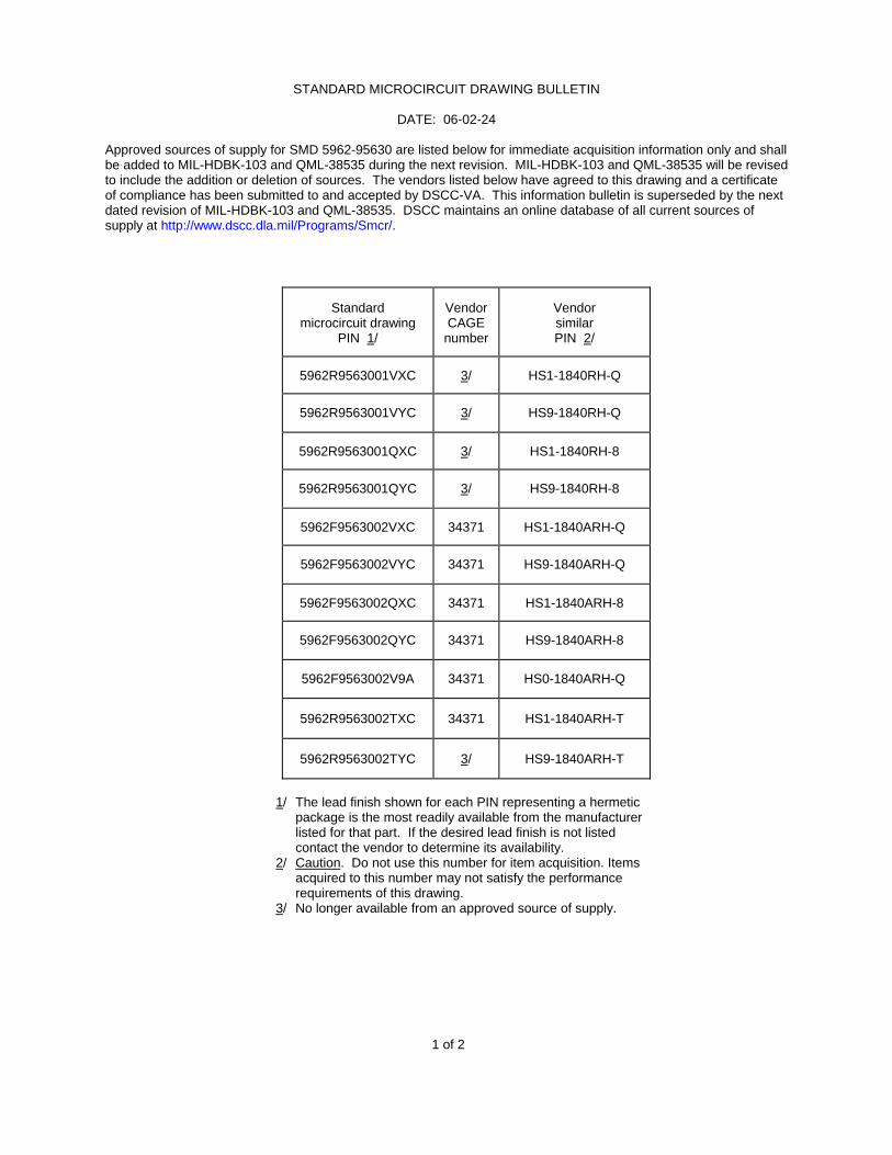
DATE: 06-02-24 Approved sources of supply for SMD 5962-95630 are listed below for immediate acquisition information only and shall be added to MIL-HDBK-103 and QML-38535 during the next revision. MIL-HDBK-103 and QML-38535 will be revised to include the addition or deletion of sources. The vendors listed below have agreed to this drawing and a certificate of compliance has been submitted to and accepted by DSCC-VA. This information bulletin is superseded by the next dated revision of MIL-HDBK-103 and QML-38535. DSCC maintains an online database of all current sources of supply at http://www.dscc.dla.mil/Programs/Smcr/.
Standard
microcircuit drawing PIN 1/
Vendor CAGE number
Vendor similar PIN 2/
5962R9563001VXC
3/
HS1-1840RH-Q
5962R9563001VYC
3/
HS9-1840RH-Q
5962R9563001QXC
3/
HS1-1840RH-8
5962R9563001QYC
3/
HS9-1840RH-8
5962F9563002VXC
34371
HS1-1840ARH-Q
5962F9563002VYC
34371
HS9-1840ARH-Q
5962F9563002QXC
34371
HS1-1840ARH-8
5962F9563002QYC
34371
HS9-1840ARH-8
5962F9563002V9A
34371
HS0-1840ARH-Q
5962R9563002TXC
34371
HS1-1840ARH-T
5962R9563002TYC
3/
HS9-1840ARH-T
1/ The lead finish shown for each PIN representing a hermetic package is the most readily available from the manufacturer listed for that part. If the desired lead finish is not listed contact the vendor to determine its availability. 2/ Caution. Do not use this number for item acquisition. Items acquired to this number may not satisfy the performance requirements of this drawing. 3/ No longer available from an approved source of supply.
1 of 2

STANDARD MICROCIRCUIT DRAWING BULLETIN - Continued
Vendor CAGE Vendor name number and address
34371 Intersil Corporation 2401 Palm Bay Blvd.
P.O. Box 883 Melbourne, FL 32902-0883
The information contained herein is disseminated for convenience only and the Government assumes no liability whatsoever for any inaccuracies in the information bulletin.
2 of 2

REVISIONS
LTR DESCRIPTION DATE (YR-MO-DA) APPROVED
REV
SHEET
REV
SHEET 15 16 17
REV STATUS REV OF SHEETS SHEET 1 2 3 4 5 6 7 8 9 10 11 12 13 14
PMIC N/A PREPARED BY Steve Duncan
DEFENSE SUPPLY CENTER COLUMBUS COLUMBUS, OHIO 43218-3990
http://www.dscc.dla.mil/ STANDARD MICROCIRCUIT
DRAWING
CHECKED BY Greg Cecil
THIS DRAWING IS AVAILABLE
FOR USE BY ALL DEPARTMENTS
APPROVED BY Charles F. Saffle
MICROCIRCUIT, HYBRID, LINEAR, DUAL 16 CHANNEL, ANALOG MULTIPLEXER AND AGENCIES OF THE
DEPARTMENT OF DEFENSE
DRAWING APPROVAL DATE 10-02-23
AMSC N/A
REVISION LEVEL
SIZE A
CAGE CODE 67268
5962-09231
SHEET 1 OF
17
DSCC FORM 2233 APR 97 5962-E417-09

STANDARD
MICROCIRCUIT DRAWING
SIZE A
5962-09231
DEFENSE SUPPLY CENTER COLUMBUS
COLUMBUS, OHIO 43218-3990
REVISION LEVEL
SHEET 2
DSCC FORM 2234 APR 97
1. SCOPE
1.1 Scope. This drawing documents five product assurance classes as defined in paragraph 1.2.3 and MIL-PRF-38534. A choice of case outlines and lead finishes which are available and are reflected in the Part or Identifying Number (PIN). When available, a choice of radiation hardness assurance levels are reflected in the PIN.
1.2 PIN. The PIN shall be as shown in the following example:
5962 - 09231 01 K X C
Federal RHA Device Device Case Lead stock class designator type class outline finish designator (see 1.2.1) (see 1.2.2) designator (see 1.2.4) (see 1.2.5)
\ / (see 1.2.3) \/ Drawing number
1.2.1 Radiation hardness assurance (RHA) designator. RHA marked devices shall meet the MIL-PRF-38534 specified RHA
levels and shall be marked with the appropriate RHA designator. A dash (-) indicates a non-RHA device.
1.2.2 Device type(s). The device type(s) identify the circuit function as follows:
Device type Generic number Circuit function
01 MUX8522 Dual 16 channel analog multiplexer, high impedance analog input 02 MUX8523 Dual 16 channel analog multiplexer, high impedance analog input with ESD protection
1.2.3 Device class designator. This device class designator shall be a single letter identifying the product assurance level. All levels are defined by the requirements of MIL-PRF-38534 and require QML Certification as well as qualification (Class H, K, and E) or QML Listing (Class G and D). The product assurance levels are as follows:
Device class Device performance documentation
K Highest reliability class available. This level is intended for use in space applications. H Standard military quality class level. This level is intended for use in applications
where non-space high reliability devices are required. G Reduced testing version of the standard military quality class. This level uses the
Class H screening and In-Process Inspections with a possible limited temperature range, manufacturer specified incoming flow, and the manufacturer guarantees (but may not test) periodic and conformance inspections (Group A, B, C, and D).
E Designates devices which are based upon one of the other classes (K, H, or G)
with exception(s) taken to the requirements of that class. These exception(s) must be specified in the device acquisition document; therefore the acquisition document should be reviewed to ensure that the exception(s) taken will not adversely affect system performance.
D Manufacturer specified quality class. Quality level is defined by the manufacturers internal, QML certified flow. This product may have a limited temperature range.
rbenson
Highlight

STANDARD
MICROCIRCUIT DRAWING
SIZE A
5962-09231
DEFENSE SUPPLY CENTER COLUMBUS
COLUMBUS, OHIO 43218-3990
REVISION LEVEL
SHEET 3
DSCC FORM 2234 APR 97
1.2.4 Case outline(s). The case outline(s) are as designated in MIL-STD-1835 and as follows:
Outline letter Descriptive designator Terminals Package style
X See figure 1 56 Ceramic quad flat pack
1.2.5 Lead finish. The lead finish shall be as specified in MIL-PRF-38534. 1.3 Absolute maximum ratings. 1/
Positive supply voltage between +VEE and GND ....................... +16.5 V dc Negative supply voltage between -VEE and GND ....................... -16.5 V dc VREF to GND ............................................................................... +16.5 V dc Digital input overvoltage range: VEN (pins 13 and 44) ............................................................... (< VREF + 4)V, (> GND - 4)V
VA (pins 14, 15, 16, and 17) .................................................... (< VREF + 4)V, (> GND - 4)V VB (Pins 40,41,42, and 43) ..................................................... (< VREF + 4)V, (> GND - 4)V Analog input overvoltage range: Device type 01 ........................................................................ -35 V dc ≤ VIN ≤ +35 V dc Device type 02 ........................................................................ -18 V dc ≤ VIN ≤ +18 V dc
Power dissipation (PD), TC = -55°C to +125°C ........................... 33 mW Thermal resistance junction-to-case (θJC) .................................. 10°C/W 2/ Storage temperature .................................................................. -65°C to +150°C Lead temperature (soldering, 10 seconds) ................................ +300°C
1.4 Recommended operating conditions.
Positive supply voltage (+VEE) 3/ ............................................... +15 V dc Negative supply voltage (-VEE) 3/ ............................................... -15 V dc VREF 3/ ........................................................................................ +5 V dc Logic low level voltage (VAL) ...................................................... +0.8 V dc Logic high level voltage (VAH) .................................................... +4.0 V dc Case operating temperature range (TC)..................................... -55°C to +125°C
2. APPLICABLE DOCUMENTS
2.1 Government specification, standards, and handbooks. The following specification, standards, and handbooks form a part
of this drawing to the extent specified herein. Unless otherwise specified, the issues of these documents are those cited in the solicitation or contract.
DEPARTMENT OF DEFENSE SPECIFICATIONS
MIL-PRF-38534 - Hybrid Microcircuits, General Specification for.
DEPARTMENT OF DEFENSE STANDARDS
MIL-STD-883 - Test Method Standard Microcircuits. MIL-STD-1835 - Interface Standard Electronic Component Case Outlines.
1/ Stresses above the absolute maximum ratings may cause permanent damage to the device. Extended operation at the maximum levels may degrade performance and affect reliability. 2/ Based on the maximum power dissipation spread over the multiplexer die. 3/ Supply voltages must be applied simultaneously or with the +VEE and -VEE supplies first, followed by VREF reference supply.

STANDARD
MICROCIRCUIT DRAWING
SIZE A
5962-09231
DEFENSE SUPPLY CENTER COLUMBUS
COLUMBUS, OHIO 43218-3990
REVISION LEVEL
SHEET 4
DSCC FORM 2234 APR 97
DEPARTMENT OF DEFENSE HANDBOOKS
MIL-HDBK-103 - List of Standard Microcircuit Drawings. MIL-HDBK-780 - Standard Microcircuit Drawings.
(Copies of these documents are available online at https://assist.daps.dla.mil/quicksearch/ or from the Standardization Document Order Desk, 700 Robbins Avenue, Building 4D, Philadelphia, PA 19111-5094.) 2.2 Order of precedence. In the event of a conflict between the text of this drawing and the references cited herein, the text of this drawing takes precedence. Nothing in this document, however, supersedes applicable laws and regulations unless a specific exemption has been obtained.
3. REQUIREMENTS
3.1 Item requirements. The individual item performance requirements for device classes D, E, G, H, and K shall be in
accordance with MIL-PRF-38534. Compliance with MIL-PRF-38534 shall include the performance of all tests herein or as designated in the device manufacturer's Quality Management (QM) plan or as designated for the applicable device class. The manufacturer may eliminate, modify or optimize the tests and inspections herein, however the performance requirements as defined in MIL-PRF-38534 shall be met for the applicable device class. In addition, the modification in the QM plan shall not affect the form, fit, or function of the device for the applicable device class.
3.2 Design, construction, and physical dimensions. The design, construction, and physical dimensions shall be as specified in MIL-PRF-38534 and herein.
3.2.1 Case outline(s). The case outline(s) shall be in accordance with 1.2.4 herein and figure 1.
3.2.2 Terminal connections. The terminal connections shall be as specified on figure 2.
3.2.3 Truth table(s). The truth table(s) shall be as specified on figure 3.
3.2.4 Switching waveform(s). The switching waveform(s) shall be as specified on figure 4. 3.2.5 Block diagram. The block diagram shall be as specified on figure 5.
3.3 Electrical performance characteristics. Unless otherwise specified herein, the electrical performance characteristics are
as specified in table I and shall apply over the full specified operating temperature range.
3.4 Electrical test requirements. The electrical test requirements shall be the subgroups specified in table II. The electrical tests for each subgroup are defined in table I.
3.5 Marking of device(s). Marking of device(s) shall be in accordance with MIL-PRF-38534. The device shall be marked with the PIN listed in 1.2 herein. In addition, the manufacturer's vendor similar PIN may also be marked.
3.6 Data. In addition to the general performance requirements of MIL-PRF-38534, the manufacturer of the device described herein shall maintain the electrical test data (variables format) from the initial quality conformance inspection group A lot sample, for each device type listed herein. Also, the data should include a summary of all parameters manually tested, and for those which, if any, are guaranteed. This data shall be maintained under document revision level control by the manufacturer and be made available to the preparing activity (DSCC-VA) upon request.
3.7 Certificate of compliance. A certificate of compliance shall be required from a manufacturer in order to supply to this drawing. The certificate of compliance (original copy) submitted to DSCC-VA shall affirm that the manufacturer's product meets the performance requirements of MIL-PRF-38534 and herein.
3.8 Certificate of conformance. A certificate of conformance as required in MIL-PRF-38534 shall be provided with each lot of microcircuits delivered to this drawing.
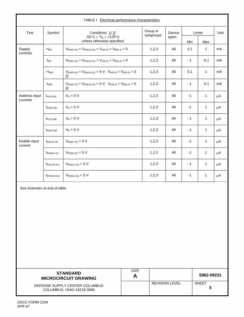
STANDARD
MICROCIRCUIT DRAWING
SIZE A
5962-09231
DEFENSE SUPPLY CENTER COLUMBUS
COLUMBUS, OHIO 43218-3990
REVISION LEVEL
SHEET 5
DSCC FORM 2234 APR 97
TABLE I. Electrical performance characteristics.
Test
Symbol
Conditions 1/ 2/
-55°C ≤ TC ≤ +125°C unless otherwise specified
Group A subgroups
Device types
Limits
Unit
Min
Max
Supply currents
+IEE
VEN(0-15) = VEN(16-31) = VA(0-3) = VB(0-3) = 0
1,2,3
All
0.1
1
mA
-IEE
VEN(0-15) = VEN(16-31) = VA(0-3) = VB(0-3) = 0
1,2,3
All
-1
-0.1
mA
+ISBY
VEN(0-15) = VEN(16-31) = 4 V, VA(0-3) = VB(0-3) = 0 3/
1,2,3
All
0.1
1
mA
-ISBY
VEN(0-15) = VEN(16-31) = 4 V, VA(0-3) = VB(0-3) = 0 3/
1,2,3
All
-1
-0.1
mA
Address input currents
IAL(0-3)A
VA = 0 V
1,2,3
All
-1
1
µA
IAH(0-3)A
VA = 5 V
1,2,3
All
-1
1
µA
IAL(0-3)B
VB = 0 V
1,2,3
All
-1
1
µA
IAH(0-3)B
VB = 5 V
1,2,3
All
-1
1
µA
Enable input current
IENL(0-15)
VEN(0-15) = 0 V
1,2,3
All
-1
1
µA
IENH(0-15)
VEN(0-15) = 5 V
1,2,3
All
-1
1
µA
IENL(16-31)
VEN(16-31) = 0 V
1,2,3
All
-1
1
µA
IENH(16-31)
VEN(16-31) = 5 V
1,2,3
All
-1
1
µA
See footnotes at end of table.
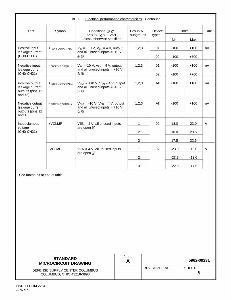
STANDARD
MICROCIRCUIT DRAWING
SIZE A
5962-09231
DEFENSE SUPPLY CENTER COLUMBUS
COLUMBUS, OHIO 43218-3990
REVISION LEVEL
SHEET 6
DSCC FORM 2234 APR 97
TABLE I. Electrical performance characteristics - Continued.
Test
Symbol
Conditions 1/ 2/
-55°C ≤ TC ≤ +125°C unless otherwise specified
Group A subgroups
Device types
Limits
Unit
Min
Max
Positive input leakage current (CH0-CH31)
+ISOFFOUTPUT(ALL)
VIN = +10 V, VEN = 4 V, output and all unused inputs = -10 V 4/ 5/
1,2,3
01
-100
+100
nA
02
-100
+700
Negative input leakage current (CH0-CH31)
-ISOFFOUTPUT(ALL)
VIN = -10 V, VEN = 4 V, output and all unused inputs = +10 V 4/ 5/
1,2,3
01
-100
+100
nA
02
-100
+700
Positive output leakage current outputs (pins 12 and 45)
+IDOFFOUTPUT(ALL)
VOUT = +10 V, VEN = 4 V, output and all unused inputs = -10 V 5/ 6/
1,2,3
All
-100
+100
nA
Negative output leakage current outputs (pins 12 and 45)
-IDOFFOUTPUT(ALL)
VOUT = -10 V, VEN = 4 V, output and all unused inputs = +10 V 5/ 6/
1,2,3
All
-100
+100
nA
Input clamped voltage (CH0-CH31)
+VCLMP
VEN = 4 V, all unused inputs are open 5/
1
02
18.0
23.0
V
2
18.0
23.5
3
17.5
22.5
-VCLMP
VEN = 4 V, all unused inputs are open 5/
1
02
-23.0
-18.0
V
2
-23.5
-18.0
3
-22.5
-17.5
See footnotes at end of table.

STANDARD
MICROCIRCUIT DRAWING
SIZE A
5962-09231
DEFENSE SUPPLY CENTER COLUMBUS
COLUMBUS, OHIO 43218-3990
REVISION LEVEL
SHEET 7
DSCC FORM 2234 APR 97
TABLE I. Electrical performance characteristics - Continued.
Test
Symbol
Conditions 1/ 2/
-55°C ≤ TC ≤ +125°C unless otherwise specified
Group A subgroups
Device types
Limits
Unit
Min
Max
Switch ON resistance outputs (pins 12 and 45)
RDS(ON)(0-31)A
VIN = +15 V, VEN = 0.8 V, IOUT = -1 mA 4/ 5/ 7/
1,2,3
All
500
3000
Ω
RDS(ON)(0-31)B
VIN = +5 V, VEN = 0.8 V, IOUT = -1 mA 4/ 5/ 7/
1,2,3
All
500
3000
Ω
RDS(ON)(0-31)C
VIN = -5 V, VEN = 0.8 V, IOUT = +1 mA 4/ 5/ 7/
1,2,3
All
500
3000
Ω
Switching tests
tAHL
RL = 10 kΩ, CL = 50 pF, See figure 4
9,10,11
All
10
1500
ns
tALH
RL = 10 kΩ, CL = 50 pF, See figure 4
9,10
All
10
2000
ns
11
10
5000
tONEN
RL = 1 kΩ, CL = 50 pF, See figure 4
9,10,11
All
10
1500
ns
tOFFEN
RL = 1 kΩ, CL = 50 pF, See figure 4
9,10,11
All
10
1000
ns
1/ +VEE = +15 V dc, -VEE = -15 V dc, and VREF = +5 V dc, unless otherwise specified. 2/ Measure inputs sequentially. Ground all unused inputs. 3/ If not tested, shall be guaranteed to the limits specified in table I. 4/ VIN is the applied input voltage to the input channels (CH0-CH31). 5/ VEN is the applied input voltage to the enable lines (0- 5) and (16-31). 6/ VOUT is the applied input voltage to the output lines OUTPUT1(0-15) and OUTPUT2(16-31). 7/ Negative current is the current flowing out of each of the pins. Positive current is the current flowing into each of the pins.

STANDARD
MICROCIRCUIT DRAWING
SIZE A
5962-09231
DEFENSE SUPPLY CENTER COLUMBUS
COLUMBUS, OHIO 43218-3990
REVISION LEVEL
SHEET 8
DSCC FORM 2234 APR 97
Case outline X.
FIGURE 1. Case outline(s).

STANDARD
MICROCIRCUIT DRAWING
SIZE A
5962-09231
DEFENSE SUPPLY CENTER COLUMBUS
COLUMBUS, OHIO 43218-3990
REVISION LEVEL
SHEET 9
DSCC FORM 2234 APR 97
Case outline X - Continued.
FIGURE 1. Case outline(s) - Continued.

STANDARD
MICROCIRCUIT DRAWING
SIZE A
5962-09231
DEFENSE SUPPLY CENTER COLUMBUS
COLUMBUS, OHIO 43218-3990
REVISION LEVEL
SHEET 10
DSCC FORM 2234 APR 97
Case outline X - Continued.
Symbol Inches Millimeters
Min Max Min Max
A .190 4.83
A1 .139 .170 3.53 4.32
A2 .005 .011 0.13 0.28
b .0135 .0195 0.34 0.50
c .005 .008 0.13 0.20
D/E .790 .810 20.07 20.57
D1 .645 .655 16.38 16.64
e .050 BSC 1.27 BSC
F .200 TYP 5.08 TYP
J .035 TYP 0.89 TYP
L 2.490 2.510 63.25 63.75
L1 2.580 65.53
L2 1.700 1.740 43.18 44.20
L3 2.090 2.110 53.09 53.59
L4 .650 TYP 16.51 TYP
N 56 56
S1 .030 TYP 0.76 TYP
S2 .015 TYP 0.38 TYP NOTES: 1. Pin 1 is indicated by an ESD triangle on top of the package and by an index on the bottom of the package. 2. The U.S. preferred system of measurement is the metric SI. This item was designed using inch-pound units of measurement. In case of problems involving conflicts between the metric and inch-pound units, the inch-pound units shall rule. 3. N equals 56, the total number of leads on the package. 4. Pin numbers are for reference only.
FIGURE 1. Case outline(s) - Continued.
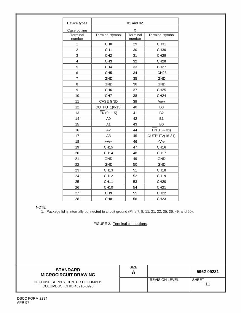
STANDARD
MICROCIRCUIT DRAWING
SIZE A
5962-09231
DEFENSE SUPPLY CENTER COLUMBUS
COLUMBUS, OHIO 43218-3990
REVISION LEVEL
SHEET 11
DSCC FORM 2234 APR 97
Device types
01 and 02
Case outline
X
Terminal number
Terminal symbol Terminal number
Terminal symbol
1 CH0 29 CH31 2 CH1 30 CH30 3 CH2 31 CH29 4 CH3 32 CH28 5 CH4 33 CH27 6 CH5 34 CH26 7 GND 35 GND 8 GND 36 GND 9 CH6 37 CH25 10 CH7 38 CH24 11 CASE GND 39 VREF 12 OUTPUT1(0-15) 40 B3 13 )150(EN − 41 B2 14 A0 42 B1 15 A1 43 B0 16 A2 44 )3116(EN − 17 A3 45 OUTPUT2(16-31) 18 +VEE 46 -VEE 19 CH15 47 CH16 20 CH14 48 CH17 21 GND 49 GND 22 GND 50 GND 23 CH13 51 CH18 24 CH12 52 CH19 25 CH11 53 CH20 26 CH10 54 CH21 27 CH9 55 CH22 28 CH8 56 CH23
NOTE: 1. Package lid is internally connected to circuit ground (Pins 7, 8, 11, 21, 22, 35, 36, 49, and 50). FIGURE 2. Terminal connections.

STANDARD
MICROCIRCUIT DRAWING
SIZE A
5962-09231
DEFENSE SUPPLY CENTER COLUMBUS
COLUMBUS, OHIO 43218-3990
REVISION LEVEL
SHEET 12
DSCC FORM 2234 APR 97
Truth table (CH0-CH15)
A3
A2
A1
A0 EN (0-15)
"ON" Channel OUTPUT1 1/ X X X X H None L L L L L CH0 L L L H L CH1 L L H L L CH2 L L H H L CH3 L H L L L CH4 L H L H L CH5 L H H L L CH6 L H H H L CH7 H L L L L CH8 H L L H L CH9 H L H L L CH10 H L H H L CH11 H H L L L CH12 H H L H L CH13 H H H L L CH14 H H H H L CH15
Truth table (CH16-CH31)
B3
B2
B1
B0 EN (16-31)
"ON" Channel OUTPUT2 2/ X X X X H None L L L L L CH16 L L L H L CH17 L L H L L CH18 L L H H L CH19 L H L L L CH20 L H L H L CH21 L H H L L CH22 L H H H L CH23 H L L L L CH24 H L L H L CH25 H L H L L CH26 H L H H L CH27 H H L L L CH28 H H L H L CH29 H H H L L CH30 H H H H L CH31
1/ Between (CH0-CH15) and OUTPUT1(0-15). 2/ Between (CH16-CH31) and OUTPUT2(16-31).
FIGURE 3. Truth table.

STANDARD
MICROCIRCUIT DRAWING
SIZE A
5962-09231
DEFENSE SUPPLY CENTER COLUMBUS
COLUMBUS, OHIO 43218-3990
REVISION LEVEL
SHEET 13
DSCC FORM 2234 APR 97
NOTE: f = 10 kHz, duty cycle = 50%.
FIGURE 4. Switching test waveform(s).

STANDARD
MICROCIRCUIT DRAWING
SIZE A
5962-09231
DEFENSE SUPPLY CENTER COLUMBUS
COLUMBUS, OHIO 43218-3990
REVISION LEVEL
SHEET 14
DSCC FORM 2234 APR 97
FIGURE 5. Block Diagram.
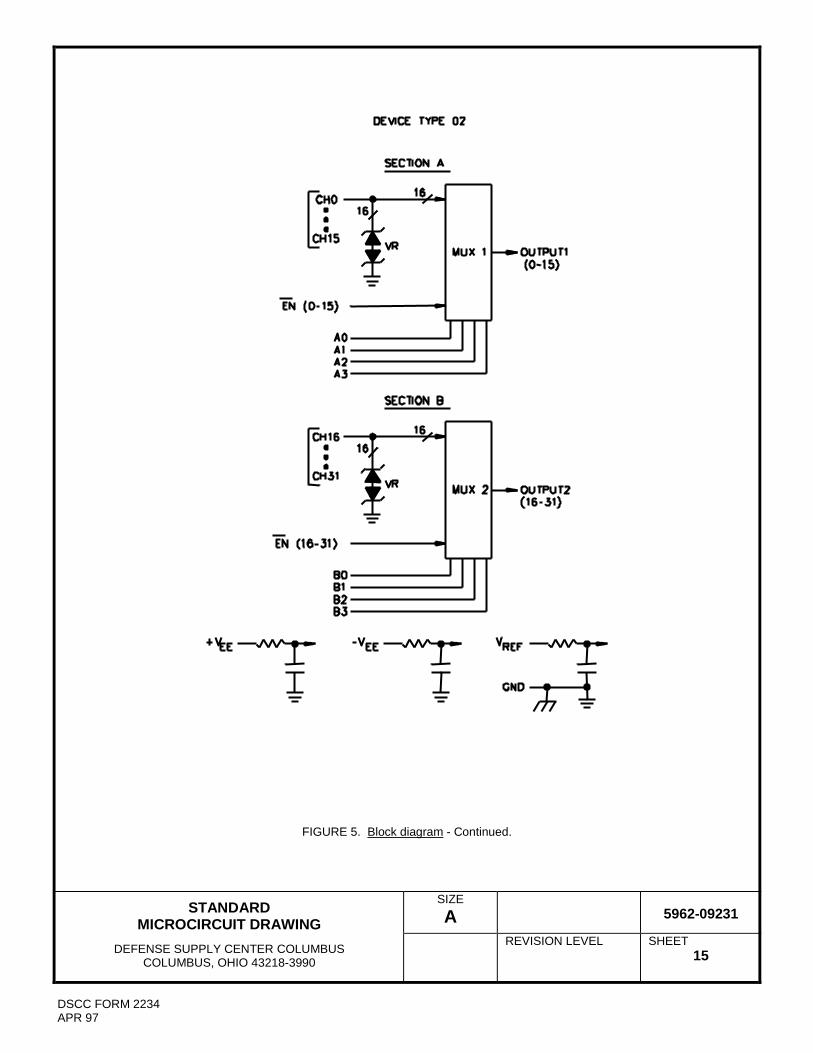
STANDARD
MICROCIRCUIT DRAWING
SIZE A
5962-09231
DEFENSE SUPPLY CENTER COLUMBUS
COLUMBUS, OHIO 43218-3990
REVISION LEVEL
SHEET 15
DSCC FORM 2234 APR 97
FIGURE 5. Block diagram - Continued.

STANDARD
MICROCIRCUIT DRAWING
SIZE A
5962-09231
DEFENSE SUPPLY CENTER COLUMBUS
COLUMBUS, OHIO 43218-3990
REVISION LEVEL
SHEET 16
DSCC FORM 2234 APR 97
TABLE II. Electrical test requirements.
MIL-PRF-38534 test requirements
Subgroups
(in accordance with MIL-PRF-38534, group A
test table) Interim electrical parameters
1, 9
Final electrical parameters
1*, 2, 3, 9, 10, 11
Group A test requirements
1, 2, 3, 9, 10, 11
Group C end-point electrical parameters
1, 2, 3, 9, 10, 11
End-point electrical parameters for radiation hardness assurance (RHA) devices
Not applicable
* PDA applies to subgroup 1.
4. VERIFICATION
4.1 Sampling and inspection. Sampling and inspection procedures shall be in accordance with MIL-PRF-38534 or as
modified in the device manufacturer's Quality Management (QM) plan. The modification in the QM plan shall not affect the form, fit, or function as described herein. 4.2 Screening. Screening shall be in accordance with MIL-PRF-38534. The following additional criteria shall apply:
a. Burn-in test, method 1015 of MIL-STD-883.
(1) Test condition A, B, C, or D. The test circuit shall be maintained by the manufacturer under document revision level control and shall be made available to either DSCC-VA or the acquiring activity upon request. Also, the test circuit shall specify the inputs, outputs, biases, and power dissipation, as applicable, in accordance with the intent specified in test method 1015 of MIL-STD-883.
(2) TA as specified in accordance with table I of method 1015 of MIL-STD-883.
b. Interim and final electrical test parameters shall be as specified in table II herein, except interim electrical parameter
tests prior to burn-in are optional at the discretion of the manufacturer.
4.3 Conformance and periodic inspections. Conformance inspection (CI) and periodic inspection (PI) shall be in accordance with MIL-PRF-38534 and as specified herein.
4.3.1 Group A inspection (CI). Group A inspection shall be in accordance with MIL-PRF-38534 and as follows:
a. Tests shall be as specified in table II herein.
b. Subgroups 4, 5, 6, 7, and 8 shall be omitted.
4.3.2 Group B inspection (PI). Group B inspection shall be in accordance with MIL-PRF-38534.

STANDARD
MICROCIRCUIT DRAWING
SIZE A
5962-09231
DEFENSE SUPPLY CENTER COLUMBUS
COLUMBUS, OHIO 43218-3990
REVISION LEVEL
SHEET 17
DSCC FORM 2234 APR 97
4.3.3 Group C inspection (PI). Group C inspection shall be in accordance with MIL-PRF-38534 and as follows:
a. End-point electrical parameters shall be as specified in table II herein.
b. Steady-state life test, method 1005 of MIL-STD-883.
(1) Test condition A, B, C, or D. The test circuit shall be maintained by the manufacturer under document revision level control and shall be made available to either DSCC-VA or the acquiring activity upon request. Also, the test circuit shall specify the inputs, outputs, biases, and power dissipation, as applicable, in accordance with the intent specified in test method 1005 of MIL-STD-883.
(2) TA as specified in accordance with table I of method 1005 of MIL-STD-883.
(3) Test duration: 1,000 hours, except as permitted by method 1005 of MIL-STD-883.
4.3.4 Group D inspection (PI). Group D inspection shall be in accordance with MIL-PRF-38534.
4.3.5 Radiation Hardness Assurance (RHA) inspection. RHA inspection is not currently applicable to this drawing.
5. PACKAGING
5.1 Packaging requirements. The requirements for packaging shall be in accordance with MIL-PRF-38534.
6. NOTES
6.1 Intended use. Microcircuits conforming to this drawing are intended for use for Government microcircuit applications
(original equipment), design applications, and logistics purposes. 6.2 Replaceability. Microcircuits covered by this drawing will replace the same generic device covered by a contractor-prepared specification or drawing.
6.3 Configuration control of SMD's. All proposed changes to existing SMD's will be coordinated as specified in MIL-PRF-
38534. 6.4 Record of users. Military and industrial users shall inform Defense Supply Center Columbus (DSCC) when a system
application requires configuration control and the applicable SMD. DSCC will maintain a record of users and this list will be used for coordination and distribution of changes to the drawings. Users of drawings covering microelectronic devices (FSC 5962) should contact DSCC-VA, telephone (614) 692-0544.
6.5 Comments. Comments on this drawing should be directed to DSCC-VA, Columbus, Ohio 43218-3990, or telephone (614)
692-1081.
6.6 Sources of supply. Sources of supply are listed in MIL-HDBK-103 and QML-38534. The vendors listed in MIL-HDBK-103 and QML-38534 have submitted a certificate of compliance (see 3.7 herein) to DSCC-VA and have agreed to this drawing.

STANDARD MICROCIRCUIT DRAWING BULLETIN DATE: 10-02-23 Approved sources of supply for SMD 5962-09231 are listed below for immediate acquisition information only and shall be added to MIL-HDBK-103 and QML-38534 during the next revisions. MIL-HDBK-103 and QML-38534 will be revised to include the addition or deletion of sources. The vendors listed below have agreed to this drawing and a certificate of compliance has been submitted to and accepted by DSCC-VA. This information bulletin is superseded by the next dated revisions of MIL-HDBK-103 and QML-38534. DSCC maintains an online database of all current sources of supply at http://www.dscc.dla.mil/Programs/Smcr/.
Standard
microcircuit drawing PIN 1/
Vendor CAGE number
Vendor similar PIN 2/
5962-0923101KXC
88379
MUX8522-201-1S
5962-0923102KXC
88379
MUX8523-201-1S
1/ The lead finish shown for each PIN representing a hermetic package is the most readily available from the
manufacturer listed for that part. If the desired lead finish is not listed contact the Vendor to determine its availability.
2/ Caution. Do not use this number for item acquisition. Items acquired to this number may not satisfy the performance requirements of this drawing.
Vendor CAGE Vendor name number and address
88379 Aeroflex Plainview Incorporated, (Aeroflex Microelectronics Solutions) 35 South Service Road Plainview, NY 11803-4193
The information contained herein is disseminated for convenience only and the Government assumes no liability whatsoever for any inaccuracies in the information bulletin.
rbenson
Highlight
rbenson
Highlight
rbenson
Highlight


![Flatpack Introduction Rev 5 September 2002 Ppt [Autoguardado]](https://static.fdocuments.us/doc/165x107/55cf96ff550346d0338f263d/flatpack-introduction-rev-5-september-2002-ppt-autoguardado.jpg)


![351400 013 UserGde Flatpack Rectifier Mod PDF[1]](https://static.fdocuments.us/doc/165x107/5451ba7baf795915308b494c/351400-013-usergde-flatpack-rectifier-mod-pdf1.jpg)

